EP3394796B1 - Electronic wireless communication device comprising two electronic chips and method for manufacturing such a device - Google Patents
Electronic wireless communication device comprising two electronic chips and method for manufacturing such a device Download PDFInfo
- Publication number
- EP3394796B1 EP3394796B1 EP16829421.3A EP16829421A EP3394796B1 EP 3394796 B1 EP3394796 B1 EP 3394796B1 EP 16829421 A EP16829421 A EP 16829421A EP 3394796 B1 EP3394796 B1 EP 3394796B1
- Authority
- EP
- European Patent Office
- Prior art keywords
- antenna
- electronic
- chip
- frequency band
- electronic chip
- Prior art date
- Legal status (The legal status is an assumption and is not a legal conclusion. Google has not performed a legal analysis and makes no representation as to the accuracy of the status listed.)
- Active
Links
- 238000004891 communication Methods 0.000 title claims description 81
- 238000000034 method Methods 0.000 title claims description 7
- 238000004519 manufacturing process Methods 0.000 title claims description 6
- 239000000758 substrate Substances 0.000 claims description 39
- 230000015572 biosynthetic process Effects 0.000 claims description 6
- 238000002955 isolation Methods 0.000 description 27
- 230000004907 flux Effects 0.000 description 18
- 230000008878 coupling Effects 0.000 description 12
- 238000010168 coupling process Methods 0.000 description 12
- 238000005859 coupling reaction Methods 0.000 description 12
- 230000003071 parasitic effect Effects 0.000 description 11
- 230000001808 coupling effect Effects 0.000 description 8
- 239000003990 capacitor Substances 0.000 description 6
- 238000010586 diagram Methods 0.000 description 4
- 230000004913 activation Effects 0.000 description 3
- 230000008859 change Effects 0.000 description 3
- 230000007423 decrease Effects 0.000 description 3
- 230000005672 electromagnetic field Effects 0.000 description 3
- 238000007639 printing Methods 0.000 description 3
- 239000000853 adhesive Substances 0.000 description 2
- 230000001070 adhesive effect Effects 0.000 description 2
- 238000006073 displacement reaction Methods 0.000 description 2
- 230000000694 effects Effects 0.000 description 2
- 238000012795 verification Methods 0.000 description 2
- 238000004804 winding Methods 0.000 description 2
- 239000000956 alloy Substances 0.000 description 1
- 229910045601 alloy Inorganic materials 0.000 description 1
- 230000001955 cumulated effect Effects 0.000 description 1
- 238000005516 engineering process Methods 0.000 description 1
- 230000003595 spectral effect Effects 0.000 description 1
Images


Classifications
-
- G—PHYSICS
- G06—COMPUTING; CALCULATING OR COUNTING
- G06K—GRAPHICAL DATA READING; PRESENTATION OF DATA; RECORD CARRIERS; HANDLING RECORD CARRIERS
- G06K19/00—Record carriers for use with machines and with at least a part designed to carry digital markings
- G06K19/06—Record carriers for use with machines and with at least a part designed to carry digital markings characterised by the kind of the digital marking, e.g. shape, nature, code
- G06K19/067—Record carriers with conductive marks, printed circuits or semiconductor circuit elements, e.g. credit or identity cards also with resonating or responding marks without active components
- G06K19/07—Record carriers with conductive marks, printed circuits or semiconductor circuit elements, e.g. credit or identity cards also with resonating or responding marks without active components with integrated circuit chips
- G06K19/072—Record carriers with conductive marks, printed circuits or semiconductor circuit elements, e.g. credit or identity cards also with resonating or responding marks without active components with integrated circuit chips the record carrier comprising a plurality of integrated circuit chips
-
- G—PHYSICS
- G06—COMPUTING; CALCULATING OR COUNTING
- G06K—GRAPHICAL DATA READING; PRESENTATION OF DATA; RECORD CARRIERS; HANDLING RECORD CARRIERS
- G06K19/00—Record carriers for use with machines and with at least a part designed to carry digital markings
- G06K19/06—Record carriers for use with machines and with at least a part designed to carry digital markings characterised by the kind of the digital marking, e.g. shape, nature, code
- G06K19/067—Record carriers with conductive marks, printed circuits or semiconductor circuit elements, e.g. credit or identity cards also with resonating or responding marks without active components
- G06K19/07—Record carriers with conductive marks, printed circuits or semiconductor circuit elements, e.g. credit or identity cards also with resonating or responding marks without active components with integrated circuit chips
- G06K19/0723—Record carriers with conductive marks, printed circuits or semiconductor circuit elements, e.g. credit or identity cards also with resonating or responding marks without active components with integrated circuit chips the record carrier comprising an arrangement for non-contact communication, e.g. wireless communication circuits on transponder cards, non-contact smart cards or RFIDs
-
- G—PHYSICS
- G06—COMPUTING; CALCULATING OR COUNTING
- G06K—GRAPHICAL DATA READING; PRESENTATION OF DATA; RECORD CARRIERS; HANDLING RECORD CARRIERS
- G06K19/00—Record carriers for use with machines and with at least a part designed to carry digital markings
- G06K19/06—Record carriers for use with machines and with at least a part designed to carry digital markings characterised by the kind of the digital marking, e.g. shape, nature, code
- G06K19/067—Record carriers with conductive marks, printed circuits or semiconductor circuit elements, e.g. credit or identity cards also with resonating or responding marks without active components
- G06K19/07—Record carriers with conductive marks, printed circuits or semiconductor circuit elements, e.g. credit or identity cards also with resonating or responding marks without active components with integrated circuit chips
- G06K19/077—Constructional details, e.g. mounting of circuits in the carrier
- G06K19/07701—Constructional details, e.g. mounting of circuits in the carrier the record carrier comprising an interface suitable for human interaction
- G06K19/07703—Constructional details, e.g. mounting of circuits in the carrier the record carrier comprising an interface suitable for human interaction the interface being visual
- G06K19/07707—Constructional details, e.g. mounting of circuits in the carrier the record carrier comprising an interface suitable for human interaction the interface being visual the visual interface being a display, e.g. LCD or electronic ink
-
- G—PHYSICS
- G06—COMPUTING; CALCULATING OR COUNTING
- G06K—GRAPHICAL DATA READING; PRESENTATION OF DATA; RECORD CARRIERS; HANDLING RECORD CARRIERS
- G06K19/00—Record carriers for use with machines and with at least a part designed to carry digital markings
- G06K19/06—Record carriers for use with machines and with at least a part designed to carry digital markings characterised by the kind of the digital marking, e.g. shape, nature, code
- G06K19/067—Record carriers with conductive marks, printed circuits or semiconductor circuit elements, e.g. credit or identity cards also with resonating or responding marks without active components
- G06K19/07—Record carriers with conductive marks, printed circuits or semiconductor circuit elements, e.g. credit or identity cards also with resonating or responding marks without active components with integrated circuit chips
- G06K19/077—Constructional details, e.g. mounting of circuits in the carrier
- G06K19/07749—Constructional details, e.g. mounting of circuits in the carrier the record carrier being capable of non-contact communication, e.g. constructional details of the antenna of a non-contact smart card
- G06K19/07766—Constructional details, e.g. mounting of circuits in the carrier the record carrier being capable of non-contact communication, e.g. constructional details of the antenna of a non-contact smart card comprising at least a second communication arrangement in addition to a first non-contact communication arrangement
- G06K19/07767—Constructional details, e.g. mounting of circuits in the carrier the record carrier being capable of non-contact communication, e.g. constructional details of the antenna of a non-contact smart card comprising at least a second communication arrangement in addition to a first non-contact communication arrangement the first and second communication means being two different antennas types, e.g. dipole and coil type, or two antennas of the same kind but operating at different frequencies
-
- G—PHYSICS
- G06—COMPUTING; CALCULATING OR COUNTING
- G06K—GRAPHICAL DATA READING; PRESENTATION OF DATA; RECORD CARRIERS; HANDLING RECORD CARRIERS
- G06K19/00—Record carriers for use with machines and with at least a part designed to carry digital markings
- G06K19/06—Record carriers for use with machines and with at least a part designed to carry digital markings characterised by the kind of the digital marking, e.g. shape, nature, code
- G06K19/067—Record carriers with conductive marks, printed circuits or semiconductor circuit elements, e.g. credit or identity cards also with resonating or responding marks without active components
- G06K19/07—Record carriers with conductive marks, printed circuits or semiconductor circuit elements, e.g. credit or identity cards also with resonating or responding marks without active components with integrated circuit chips
- G06K19/077—Constructional details, e.g. mounting of circuits in the carrier
- G06K19/07749—Constructional details, e.g. mounting of circuits in the carrier the record carrier being capable of non-contact communication, e.g. constructional details of the antenna of a non-contact smart card
- G06K19/07773—Antenna details
- G06K19/07794—Antenna details the record carrier comprising a booster or auxiliary antenna in addition to the antenna connected directly to the integrated circuit
-
- H—ELECTRICITY
- H01—ELECTRIC ELEMENTS
- H01Q—ANTENNAS, i.e. RADIO AERIALS
- H01Q1/00—Details of, or arrangements associated with, antennas
- H01Q1/12—Supports; Mounting means
- H01Q1/22—Supports; Mounting means by structural association with other equipment or articles
- H01Q1/2208—Supports; Mounting means by structural association with other equipment or articles associated with components used in interrogation type services, i.e. in systems for information exchange between an interrogator/reader and a tag/transponder, e.g. in Radio Frequency Identification [RFID] systems
- H01Q1/2225—Supports; Mounting means by structural association with other equipment or articles associated with components used in interrogation type services, i.e. in systems for information exchange between an interrogator/reader and a tag/transponder, e.g. in Radio Frequency Identification [RFID] systems used in active tags, i.e. provided with its own power source or in passive tags, i.e. deriving power from RF signal
-
- H—ELECTRICITY
- H01—ELECTRIC ELEMENTS
- H01Q—ANTENNAS, i.e. RADIO AERIALS
- H01Q1/00—Details of, or arrangements associated with, antennas
- H01Q1/36—Structural form of radiating elements, e.g. cone, spiral, umbrella; Particular materials used therewith
- H01Q1/38—Structural form of radiating elements, e.g. cone, spiral, umbrella; Particular materials used therewith formed by a conductive layer on an insulating support
Definitions
- the present invention relates to the field of electronic wireless communication devices, comprising at least two electronic chips, each being associated with a respective antenna in order to communicate with an external terminal.
- the invention applies in particular, but not exclusively, to smart cards, such as bank cards of ID-1 format specified in the ISO 7810 standard, having the dimensions 85.6 millimeters by 53.98 millimeters by 0 , 76 millimeters and comprising two electronic chips.
- an electronic wireless communication device such as a smart card
- the figure 1 shows such an electronic wireless communication device 100, taking the form of a smart card.
- the device 100 comprises a first electronic chip 102 and a second electronic chip 104.
- the first electronic chip 102 is electrically connected to a first antenna 106, and is configured to communicate with an external terminal by means of the first antenna 106 according to a first communication protocol.
- the first electronic chip 102 has a contactless payment function.
- the second electronic chip 104 is electrically connected to a second antenna 108, and is configured to communicate with an external terminal by means of the second antenna 108 according to a second communication protocol.
- the second electronic chip 104 has a function of controlling a dynamic verification code display (“motion code” in English terminology) of the device 100.
- the operational communication frequency band of the assembly comprising the first electronic chip 102 and the first antenna 106 is more large that the operational communication frequency band of the assembly comprising the second electronic chip 104 and the second antenna 108, and the two operational communication frequency bands are very close because included in the communication frequency band of a terminal external.
- the first antenna 106 is of fairly large dimensions.
- the second antenna 108 is of fairly large dimensions, however less important than the dimensions of the first antenna 106 .
- the small size of the device 100 and the large size of the two antennas 106 and 108 implies that the antennas 106, 108 are arranged close to one another in the device 100. This physical proximity of the antennas 106, 108 gives rise to a phenomenon parasitic electromagnetic coupling between the two antennas 106, 108.
- the parasitic electromagnetic coupling degrades the performance of the antennas 106, 108 which implies communication problems for each antenna 106, 108.
- the second antenna 108 consumes energy and causes a displacement of the operational frequency band of the assembly comprising the first chip 102 and the first antenna 106, because the effective flux picked up by the first antenna 106 in the presence of the second antenna 108 is reduced, which implies reduced inductance and a resonant frequency shifted towards high frequencies.
- the personalization, by an external terminal, of the first electronic chip 102, as well as the payment by means of the first electronic chip 102 is thus difficult to implement, for example because the operational frequency band of the assembly comprising the first chip 102 and the first antenna 106 is no longer included in the optimized communication frequency band of the external terminal.
- the first antenna 106 consumes energy, which causes a displacement of the operational frequency band of the assembly. comprising the second chip 104 and the second antenna 108.
- the personalization, by an external terminal, of the second electronic chip 104 is then difficult to implement.
- the document JP 2003-331238 describes an integrated circuit card.
- the communication frequency band of an assembly comprising the first electronic chip and the first pair of antennas being widened relative to the communication frequency band of an assembly comprising the first electronic chip and the first antenna, the first chip can communicate with a larger number of external terminals.
- the communication frequency band of an assembly comprising the second electronic chip and the second pair of antennas being widened with respect to the communication frequency band of an assembly comprising the second electronic chip and the second antenna, the second chip can communicate with a greater number of external terminals.
- the first antenna forms with the third antenna a first pair of antenna, it is possible to reduce the size of the first antenna while maintaining good communication performance. Indeed, the third antenna makes it possible to capture more electromagnetic flux.
- the second antenna forming with the third antenna a second pair of antennas, it is possible to reduce the size of the second antenna while maintaining good communication performance.
- the dimensions of the first antenna and of the second antenna being reduced, it is possible to move the first antenna away from the second antenna and to arrange it so as to limit the parasitic coupling effect between the first and second antennas.
- the area delimited by the third antenna is greater than the area delimited by the first antenna and / or the area delimited by the second antenna.
- the large dimensions of the third antenna allow the third antenna to pick up a large electromagnetic flux, which is accumulated with the flux picked up by the first antenna or to the stream picked up by the second antenna. It is thus possible to reduce the dimensions of the first antenna and of the second antenna while maintaining good communication performance.
- the dimensions of the first antenna and of the second antenna being reduced, it is possible to move the first antenna away from the second antenna and to arrange it so as to limit the parasitic coupling effect between the first and second antennas.
- the surface delimited by the first antenna is substantially identical to the surface delimited by the second antenna.
- the performance of the first antenna is substantially equal to the performance of the second antenna, and it is possible to use the same external communication terminal to communicate with the two electronic chips.
- the first antenna is arranged at a first distance from the second antenna and at a second distance from the third antenna, the first distance being greater than the second distance.
- the third antenna is substantially planar and the first, second and third antennas are arranged such that the projection of the first antenna in the plane of the third antenna extends outside the third antenna and the projection of the second antenna in the plane of the third antenna extends inside the third antenna.
- the operating frequency band of the third antenna taken in isolation is greater than the operating frequency band of a first assembly comprising the first electronic chip and the first antenna taken in isolation or than the frequency band.
- operating frequency of a second assembly comprising the second electronic chip and the second antenna taken in isolation.
- the width of the operating frequency band of a first assembly comprising the first electronic chip and the first antenna taken in isolation is substantially identical to the operating frequency band of a second assembly comprising the second electronic chip and the second antenna taken in isolation.
- the same external terminal can be used to communicate with the first electronic chip and the second electronic chip.
- the communication protocol of the first electronic chip is defined by the ISO 14443 standard and the communication protocol of the second electronic chip is defined by the ISO 15693 standard.
- the first electronic chip is configured to make a payment and the second electronic chip is configured to control an electronic component of said device.
- the electronic component is a screen suitable for displaying a security code.
- the device comprises identification digits, the security code being intended to be used in combination with the identification digits to make a payment.
- the electronic device is a smart card of ID-1 format defined by the ISO 7810 standard.
- the present invention relates to the field of electronic wireless communication devices, comprising at least two electronic chips, each being associated with a respective antenna in order to communicate with an external terminal.
- the figure 2 is a top view, in transparency, of an electronic wireless communication device 200 in accordance with an exemplary embodiment of the invention.
- the device 200 comprises a first electronic chip 202 and a second electronic chip 204.
- the device 200 further comprises a first antenna 206, electrically connected to the first electronic chip 202, and a second antenna 208 electrically connected to the second electronic chip 204.
- the device 200 comprises a third antenna 210, adapted to be electromagnetically coupled with the first antenna 206, so that the first electronic chip 202 is configured to communicate with a first external terminal, according to a first protocol, by means of of a first antenna pair formed by the first antenna 206 and the third antenna 210.
- the third antenna 210 is adapted to be electromagnetically coupled with the second antenna 208, so that the second electronic chip 204 is configured to communicate with the first external terminal and / or a second external terminal, according to a second protocol. , by means of a second antenna pair formed by the second antenna 208 and the third antenna 210.
- a first antenna pair formed by the first antenna 206 and the third antenna 210 is meant that the first antenna pair is formed by the coupling of the first antenna 206 with the third antenna 210.
- a second antenna pair formed by the second antenna 208 and the third antenna 210 it is understood that the second antenna pair is formed by the coupling of the second antenna 208 with the third antenna 210.
- the first electronic chip 202 as well as the first antenna 206 form a first communication assembly 212.
- the second electronic chip 204 as well as the second antenna 208 form a second communication assembly 214.
- the first electronic chip 202 together with the first antenna 206 coupled to the third antenna 210, i.e. the first pair of antennas, form a third communication assembly 216. Further, the second electronic chip 204 thus that the second antenna 208 coupled to the third antenna 210, i.e. the second antenna pair, form a fourth communication assembly 218.
- the device 200 comprises more than two electronic chips. Each electronic chip is then electrically connected to a respective antenna, each antenna being coupled with the same coupling antenna.
- the figure 3 shows an electrical diagram corresponding to a device 200 in accordance with an exemplary embodiment of the invention, for example to the device of the figure 2 , of the figure 5 , or the figure 11 . More precisely, the electrical diagram shows the detail of the equivalent circuit of each antenna 206, 208, 210 and electronic chip 202, 204, as well as the mutual coupling between the third antenna 210 and the two other antennas 206, 208.
- the electrical diagram comprises a first RLC circuit 300 corresponding to the first communication assembly 212, a second RLC circuit 302 corresponding to the second communication assembly 214, and a third RLC circuit 304 corresponding to the third antenna.
- the first RLC circuit 300 comprises a first coil L a1 connected in parallel to a first capacitor C n1 and a first resistor R a1 .
- the first coil L a1 corresponds to the impedance of the first antenna 206
- the first resistor R a1 corresponds to the resistance of the first antenna 206
- the first capacitor C n1 corresponds to the capacitance of the first antenna 206 added to the capacitance of the first electronic chip 202.
- the second RLC circuit 302 comprises a second coil L a2 connected in parallel to a second capacitor C n2 and a second resistor R a2 .
- the second coil L a2 corresponds to the impedance of the second antenna 208
- the second resistance R a2 corresponds to the resistance of the second antenna 208
- the second capacitor C n2 corresponds to the capacity of the second antenna 208 added to the capacity of the second electronic chip 204.
- the third RLC circuit 304 comprises a third assembly comprising a third coil L a3 connected in parallel to a third capacitor C a3 and a third resistor R a3 .
- the third coil L a3 corresponds to the impedance of the third antenna 210
- the third resistor R a3 corresponds to the resistance of the third antenna 210
- the third capacitor C a3 corresponds to the capacity of the third antenna 210.
- the coupling M1 between the first coil L a1 of the first RLC circuit 300 and the third coil L a3 of the third RLC circuit 304 represents the coupling between the first antenna 206 and the third antenna 210.
- the coupling M2 between the second coil L a2 of the second RLC circuit 302 and the third coil L a3 of the third RLC circuit 304 represents the coupling between the second antenna 208 and the third antenna 210.
- the third antenna 210 is electromagnetically coupled with the first antenna 206, electromagnetically coupled with the second antenna 208, is not electrically connected to the first chip 202, and is not electrically connected to the second chip 204 .
- the figure 4 schematically represents operating frequency bands of a device 200 according to an exemplary embodiment of the invention, for example the device of the figure 2 , of the figure 5 , or the figure 11 .
- the first assembly 212 taken in isolation operates in a first frequency band ⁇ F1
- the second assembly 214 taken in isolation operates in a second frequency band ⁇ F2
- the third antenna 210 taken in isolation operates in a frequency band ⁇ F3.
- the third assembly 216 When the first electronic chip 202 is activated, the third assembly 216 operates in a fourth operating frequency band ⁇ F13 or operational communication.
- the fourth frequency band ⁇ F13 comprises the first frequency band ⁇ F1 and is wider than the first frequency band ⁇ F1.
- the fourth assembly 218 operates in a fifth frequency band ⁇ F23 of operation or of operational communication.
- the fifth frequency band ⁇ F23 comprises the second frequency band ⁇ F2 and is wider than the second frequency band ⁇ F2.
- the fourth frequency band ⁇ F13 and the fifth frequency band ⁇ F23 have a common frequency range, corresponding approximately to the third frequency band ⁇ F3.
- a terminal communicating at a frequency included in the common frequency range can communicate with the first electronic chip 202, if the terminal communicates according to the first protocol, or with the second electronic chip 204, if the terminal communicates according to the second protocol.
- the figure 4 also shows a sixth frequency band ⁇ F6 of operation of an external terminal, for example the first external terminal or the second external terminal.
- the first electronic chip 202 communicates with a terminal, for example the first terminal, by means of the first pair of antennas, at a frequency of about 13.56 megahertz, for example 13.56 megahertz.
- the second electronic chip 204 communicates with said terminal and / or another terminal, for example the second terminal, by means of the second pair of antennas, at a frequency of approximately 13.56 megahertz, for example 13.56 megahertz.
- the fourth frequency band ⁇ F13 being widened compared to the first frequency band ⁇ F1, the first chip 202 can communicate with a greater number of external terminals. Indeed, the external terminals do not all operate according to the same frequency band.
- the second chip 204 can communicate with a greater number of external terminals.
- the fourth frequency band ⁇ F13 or the fifth frequency band ⁇ F23 represents a subset of the overall resonance template of the device 200.
- the first antenna 206 forms with the third antenna 210 a first pair of antennas, it is possible to reduce the size of the first antenna 206 while maintaining good communication performance. Indeed, the third antenna 210 makes it possible to capture more electromagnetic flux.
- the second antenna 208 forming with the third antenna 210 a second pair of antennas, it is possible to reduce the size of the second antenna 208 while maintaining good communication performance.
- the dimensions of the first antenna 206 and of the second antenna 208 being reduced, it is possible to move the first antenna 206 away from the second antenna 208 and to arrange it so as to limit the parasitic coupling effect between the first and second antennas 206, 208.
- the first electronic chip 202 is on standby and the second electronic chip 204 is on standby.
- the first electronic chip 202 When the device 200 is placed in the electromagnetic field of an external terminal communicating according to the first protocol, for example the first external terminal, the first electronic chip 202 is activated after recognition of the first protocol, while the second chip 204 remains on standby .
- the device 200 then has the fourth frequency band ⁇ F13, in which effective communication with the external terminal is possible.
- the first chip 202 and the external terminal can thus communicate in the fourth frequency band ⁇ F13 according to the first protocol, the second antenna 208, associated with the second protocol, then having no effect, since it has silent resonance.
- the energy transfer that is to say the electromagnetic flux picked up, is then greater for the first pair of antennas associated with the first electronic chip 202, that is to say the third assembly 216.
- the activation of the first electronic chip 202 increases the capacity of the first electronic chip 202, which decreases the resonant frequency of the third set 216 in order to match said resonant frequency to the resonant frequency of the external terminal.
- the second electronic chip 204 When the device 200 is placed in the electromagnetic field of an external terminal communicating according to the second protocol, for example the first external terminal or the second external terminal, the second electronic chip 204 is activated after recognition of the second protocol, while the first chip 202 remains on standby. The device 200 then has the fifth frequency band ⁇ F23, in which effective communication with the external terminal is possible.
- the second chip 204 and the external terminal can thus communicate in the fifth frequency band ⁇ F23 according to the second protocol, the first antenna 206, associated with the first protocol, then having no effect, because in silent resonance.
- the energy transfer that is to say the electromagnetic flux picked up, is then greater for the second pair of antennas associated with the second electronic chip 204, that is to say the fourth assembly 218.
- the activation of the second electronic chip 204 increases the capacitance of the second electronic chip 204, which decreases the resonant frequency of the fourth assembly 218 in order to set said resonant frequency to the resonant frequency of the external terminal.
- the device 200 is for example a smart card.
- the device 200 is another electronic document, such as an electronic passport, an electronic identity card or the like, an RFID module (“RFID tag” in English terminology), or a connected object.
- RFID tag RFID tag
- the communication protocol of the first chip is defined by the ISO 14443 standard. Further, in one example, the communication protocol of the second chip is defined by the ISO 15693 standard.
- the first electronic chip 202 is configured to make a payment.
- the first electronic chip 202 thus has a contactless payment function.
- a second electronic chip is then necessary to manage another function or application, because banking organizations require that a dedicated payment chip does not manage other applications, for security reasons.
- the second chip 204 is configured to control an electronic component of said device 200.
- the second electronic chip 204 has for example a function of controlling a dynamic verification code display (“motion code” in English terminology). ) of the device 200, that is to say of a screen suitable for displaying a security code.
- Each antenna 206, 208, 210 takes the form of a winding comprising at least one turn, the winding being substantially planar.
- the antennas 206, 208, 210 are thus substantially flat.
- the first antenna 206 extends over a first plane
- the second antenna 208 extends over a second plane
- the third antenna 210 extends over a third plane.
- the first, second and third planes are substantially parallel to each other and at least two of the first, second and third planes can be merged.
- the third antenna 210 may have larger dimensions than the first antenna 206 and larger dimensions than the second antenna 208.
- the area delimited by the third antenna 210 may be greater than the area delimited by the first antenna 206.
- the area delimited by the third antenna 210 may be greater than the area delimited by the second antenna 208.
- the area of the third plane delimited by the third antenna 210 may be greater than the area of the first plane delimited by the first antenna 206.
- the area of the third plane delimited by the third antenna 210 may be greater than the area of the second plane bounded by the second antenna 208.
- the area delimited by the third antenna 210 is for example twice as large as the area delimited by the first antenna 206, and is for example twice as large as the area delimited by the second antenna 208.
- the large dimensions of the third antenna 210 allow the third antenna 210 to pick up a large electromagnetic flux, which is cumulated with the flux picked up by the first antenna 206 or with the flux picked up by the second antenna 208.
- the first antenna 206 In order to operate the first chip 202, the first antenna 206 thus does not need to pick up as much magnetic flux as the flux necessary for the first antenna 106 of the figure 1 to operate the first chip 102 of the figure 1 . It is possible to reduce the dimensions of the first antenna 206 while maintaining good communication performance.
- the second antenna 208 thus does not need to capture as much magnetic flux as the flux necessary for the second antenna 108 of the figure 1 to operate the second chip 104 of the figure 1 . It is possible to reduce the dimensions of the second antenna 208 while maintaining good communication performance.
- the dimensions of the first antenna 206 and of the second antenna 208 being reduced, it is possible to move the first antenna 206 away from the second antenna 208 and to arrange it so as to limit the parasitic coupling effect between the first and second antennas 206, 208.
- the area delimited by the first antenna 206 is substantially identical to the area delimited by the second antenna 208. More precisely, the area of the first plane delimited by the first antenna 206 is substantially identical to the area of the second plane delimited by the second antenna 208.
- the performance of the first antenna 206 is substantially equal to the performance of the second antenna 208, and it is possible to use the same external communication terminal to communicate with the two electronic chips 202, 204. It is It is then sufficient to control the external terminal in order to use the first communication protocol to communicate with the first electronic chip 202, and the second communication protocol to communicate with the second electronic chip 204.
- the first antenna 206 may have an elongated shape defining a length and a width of the first antenna 206.
- the second antenna 208 substantially planar, may have an elongated shape defining a length and a width of the second. antenna 208.
- the third antenna 210 which is substantially planar, may have a shape elongate defining a length and a width of the third antenna 210.
- the first, second and third antennas 206, 208, 210 can then be arranged such that the projection of the longitudinal direction of the first antenna 206 in the plane of the third antenna 210 is parallel to the lateral direction of the third antenna 210, and so that the projection of the longitudinal direction of the second antenna 208 in the plane of the third antenna 210 is parallel to the longitudinal direction of the third antenna 210.
- the parasitic coupling effect between the first antenna 206 and the second antenna 208 is thus reduced.
- the antennas 206, 208, 210 are for example of substantially rectangular shape.
- the first, second and third antennas 206, 208, 210 are arranged such that the projection of the length of the first antenna 206 in the plane of the third antenna 210 is parallel to the width of the third antenna 210 , and so that the projection of the length of the second antenna 208 in the plane of the third antenna 210 is parallel to the length of the third antenna 210.
- first, second and third antennae 206, 208, 210 may be arranged such that the projection of the longitudinal direction of the first antenna 206 in the plane of the third antenna 210 is parallel to the longitudinal direction of the third antenna 210, and so that the projection of the longitudinal direction of the second antenna 208 in the plane of the third antenna 210 is parallel to the lateral direction of the third antenna 210.
- the first antenna 206 is disposed at a first distance from the second antenna 208 and at a second distance from the third antenna 210, the first distance possibly being greater than the second distance. The first antenna 206 is thus closer to the third antenna 210 than to the second antenna 208.
- the second antenna 208 is disposed at a third distance from the third antenna 210, the first distance possibly being greater than the third distance.
- the second antenna 208 is thus closer to the third antenna 210 than to the first antenna 206.
- the projection of the first antenna 206 in the third plane of the third antenna 210 is arranged at a first minimum distance D1 from the projection of the second antenna 208 in the third plane and at a second minimum distance D2 from the third antenna 210, the first minimum distance D1 being greater than the second minimum distance D2.
- the projection of the second antenna 208 in the third plane is arranged at a third minimum distance D3 from the third antenna 210, the first minimum distance D1 being greater than the third minimum distance D3.
- the first, second and third antennae 206, 208, 210 can be arranged such that the projection of the first antenna 206 in the third plane of the third antenna 210 extends outside the third antenna 210 and the projection of the second antenna 208 extends inside the third antenna 210.
- the third antenna 210 thus separates the first antenna 206 from the second antenna 208, which makes it possible to reduce the parasitic coupling effect between the first and second antennas 206, 208.
- the length of the first antenna 206 is substantially equal to the width of the third antenna 210.
- the length of the second antenna 208 is little less than the length of the smallest turn of the third antenna 210.
- the first, second and third antennas 206, 208, 210 may be arranged such that the projection of the first antenna 206 in the third plane of the third antenna 210 extends inside the third antenna 210 and the projection of the second antenna 208 extends inside the third antenna 210.
- the device 200 comprises a card body, comprising a first layer, the first and second electronic chips 202, 204 as well as the first, second and third antennas 206, 208, 210 that can be placed on the same face or on different sides of the first layer.
- the card body may include at least one additional layer positioned on one face of the first layer.
- the device 200 may include at least one additional layer positioned on the other face of the first layer.
- Each additional layer may be a layer suitable for receiving a printing pattern or a transparent layer suitable for protecting the printing layer.
- the first electronic chip 202 and the first antenna 206 are positioned on a first printed circuit, or the first electronic chip 202 is positioned on the first printed circuit.
- the first printed circuit may include contact pads capable of connecting the first chip 202 to an external terminal so that the first chip 202 can also communicate with an external terminal via the contact pads.
- the card body then comprises a first cavity in which the first printed circuit is positioned.
- the second chip 204 and the second antenna 208 are positioned on a second printed circuit.
- the card body then comprises a second cavity in which the second printed circuit is positioned.
- the smart card comprises a screen suitable for displaying a security code, the screen being able to be positioned on the second printed circuit.
- the smart card can also include identification digits, for example positioned on the surface of the card body, the security code being intended to be used in combination with the identification digits to make a payment, for example a payment. on the Internet.
- the smart card is of ID-1 format defined by the ISO 7810 standard.
- the card body is then of dimensions of 85.6 millimeters by 53.98 millimeters by 0.76 millimeters.
- the figure 11 is a top view, in transparency, of an electronic wireless communication device 200 according to an exemplary embodiment of the invention, taking the form of a smart card.
- the figure 12 is a sectional view AA of the electronic wireless communication device of the figure 11 .
- the device 200 differs from the device of the figure 5 in that it comprises a body card 1100, a module 1110 comprising a first printed circuit 1112, and a second printed circuit 1120.
- the card body 1100 comprises a first layer 1102 in which the third antenna 210 is disposed and in which the first antenna 206 can be disposed.
- the first antenna 206 is disposed on the first printed circuit 1112.
- the card body 1100 may further include a second layer 1104 positioned on one side of the first layer 1102. Additionally, the card body 1100 may include a third layer 1106 and a fourth layer 1108, the first layer 1102 and the possible second layer 1104 being positioned between the third layer 1106 and the fourth layer 1108.
- the first and second layers 1102, 1104 are layers adapted to receive a printing pattern and the third and fourth layers 1106, 1108 are layers adapted to protect the first and second layers 1102, 1104.
- the card body 1100 has a first cavity 1116, at least partially crossing the first layer 1102 and, in one example, the third layer 1106.
- the first cavity 1116 may be. positioned so as to be surrounded, in top view, by the first antenna 206 (cf. figure 11 ).
- the first chip 202 as well as contact pads 1114, able to connect the first chip 202 to an external terminal so that the first chip 202 can also communicate with an external terminal via the contact pads, are arranged on the first printed circuit. 1112.
- the module 1100 is placed in the first cavity 1116.
- the first chip 202 is electrically connected to the first antenna 206 by connection means known to those skilled in the art in the field of smart cards, for example an anisotropic adhesive. , a bump of conductive alloy or conductive wires.
- the card body 1100 comprises a second cavity 1118, passing through the first layer 1102 and possibly the second layer 1104.
- the second cavity is positioned so as to be surrounded, in top view, by the third antenna 210 (cf. figure 11 ).
- the second printed circuit 1120 is arranged in the second cavity 1118 and can be held in second cavity 1118 by means of an adhesive.
- the second antenna 208 and the second electronic chip 204 are arranged on the second printed circuit 1120.
- the second printed circuit may further include a screen 1122 adapted to display a security code.
- identification digits may be formed on the surface of the card body 1100, for example the third layer 1016.
- the third operating frequency band ⁇ F3 of the third antenna 210 taken in isolation may be greater than the first operating frequency band ⁇ F1 of the first assembly 212 taken in isolation, as shown for example by the figure 4 .
- the third operating frequency band ⁇ F3 of the third antenna 210 taken in isolation may be greater than the second operating frequency band ⁇ F2 of the second assembly 214 taken in isolation.
- the width of the first operating frequency band ⁇ F1 of the first assembly 212 taken in isolation can be substantially identical to the second operating frequency band ⁇ F2 of the second assembly 214 taken in isolation.
- the width of the fourth operating frequency band ⁇ F13 of the third assembly 216 is then substantially identical to the fifth frequency band ⁇ F23 of the fourth assembly 218, which makes it possible to use the same external terminal to communicate with the first electronic chip 202 and the second electronic chip 204.
- the fourth frequency band ⁇ F13 of the third set 216 is continuous.
- the fifth frequency band ⁇ F23 of the fourth set 218 can be continuous.
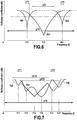
- the figure 6 shows an example of the change in reflection coefficients of a device 200 in accordance with an exemplary embodiment of the invention, for example the device 200 of the figure 2 , of the figure 5 , or the figure 11 .
- the figure 6 shows an example of a first curve 600 showing the evolution of the reflection coefficient of the first assembly 212 taken in isolation, as a function of the frequency, an example of a second curve 602 showing the evolution of the reflection coefficient of the second assembly 214 taken separately, as a function of frequency, and an example of a third curve 604 showing the change in the reflection coefficient of the third antenna 210 taken in isolation, as a function of frequency.
- the first operating frequency band ⁇ F1 of the first assembly 212 taken in isolation corresponds to the frequencies for which the values of the reflection coefficient curve 600 are the lowest.
- the reflection coefficient is lowest at a first resonant frequency Fr1 of the first assembly 212, said resonant frequency Fr1 being included in the first frequency band ⁇ F1.
- the second operating frequency band ⁇ F2 of the second assembly 214 taken in isolation corresponds to the frequencies for which the values of the reflection coefficient curve 602 are the lowest.
- the reflection coefficient is lowest at a second resonant frequency Fr2 of the second assembly 214, said resonant frequency Fr2 being included in the second frequency band ⁇ F2.
- the third operating frequency band ⁇ F3 of the third antenna 210 taken in isolation corresponds to the frequencies for which the values of the reflection coefficient curve 604 are the lowest.
- the reflection coefficient is the lowest at a third resonant frequency Fr3 of the third antenna 210 taken in isolation, included in the third frequency band ⁇ F3.
- the third resonant frequency Fr3 is higher than the first resonant frequency Fr1, and is lower than the second resonant frequency Fr2.
- the figure 7 shows examples of resonance templates of the device 200 of the figure 6 . More precisely, the figure 7 represents a resonance template 700 of the resonant assembly formed by the three antennas 206, 208, 210 and the two electronic chips 202, 204 having the changes in reflection coefficient described in figure 6 , when the two electronic chips 202, 204 are on standby.
- the term “resonance template” is understood to mean the energy transfer values in the resonant frequency band of the resonant assembly.
- the resonant frequency band is the frequency band over which the device 200 is capable of receive or send electromagnetic energy.
- the resonant frequency band is wider than and includes the fourth frequency band ⁇ F13 for which communication can be established.
- the resonant frequency band is wider than and includes the fifth frequency band ⁇ F23 for which communication can be established.
- the figure 7 also represents a resonance template 702 of the assembly formed by the three antennas 206, 208, 210 and the two electronic chips 202, 204 having the changes in reflection coefficient described in figure 6 , when the first electronic chip 202 is activated and when the second electronic chip 204 is on standby, for communication with a given external terminal.
- the figure 7 represents a resonance template 704 of the resonant assembly formed by the three antennas 206, 208, 210 and the two electronic chips 202, 204 having the changes in reflection coefficient described in figure 6 , when the second electronic chip 204 is activated and when the first electronic chip 202 is on standby, for communication with a given external terminal, and when the parameters L a1 , C n1 and R a1 of the first set 212 are substantially identical to the parameters L a2 , C n2 and R a2 of the second set 214.
- the figure 7 shows that the three antennas 206, 208, 210 and the two electronic chips 202, 204 are configured such that the activation of the first electronic chip 202 or of the second electronic chip 204 decreases the resonance frequencies. This is explained by the increase in the capacity of an electronic chip 202, 204 when the electronic chip 202, 204 is activated.
- the parameters L a1 , C n1 and R a1 of the first set 212 being substantially identical to the parameters L a2 , C n2 and R a2 of the second set 214, the curve 702 and the curve 704 are substantially superimposed.
- the first electronic chip 202 When the first electronic chip 202 is activated, the first electronic chip 202 communicates according to the fourth frequency band ⁇ F13.
- the frequency band of the template 702 outside the fourth frequency band ⁇ F13 is not used to communicate, but the electromagnetic flux of this frequency band is received.
- the second electronic chip 204 when the second electronic chip 204 is activated, the second electronic chip 204 communicates according to the fifth frequency band ⁇ F23.
- the frequency band of the template 704 outside the fifth frequency band ⁇ F23 is not used to communicate, but the electromagnetic flux of this frequency band is received.
- the configuration of the resonance frequencies described with reference to the figure 6 allows the fourth frequency band ⁇ F13 to be continuous, and allows the fifth frequency band ⁇ F23 to be continuous.
- the resonant frequency Fr3 of the third antenna 210 taken in isolation may be lower than the resonant frequency Fr1, and may be greater than the resonant frequency Fr2.
- the figure 8 shows another example of the change in reflection coefficients of a device 200 in accordance with an exemplary embodiment of the invention, for example the device 200 of the figure 2 , of the figure 5 , or the figure 11 .
- the figure 8 shows an example of a first curve 800 showing the evolution of the reflection coefficient of the first assembly 212 taken in isolation, as a function of the frequency, an example of a second curve 802 showing the evolution of the reflection coefficient of the second assembly 214 taken in isolation, in function of the frequency, and an example of a third curve 804 showing the evolution of the reflection coefficient of the third antenna 210 taken in isolation, as a function of the frequency.
- the resonant frequency Fr3 of the third antenna 210 taken in isolation is greater than the resonant frequency Fr1, and is greater than the resonant frequency Fr2.
- the figure 9 represents an example of the resonance template of the device of the figure 8 , or more precisely a resonance template of the assembly formed by the three antennas 206, 208, 210 and the two electronic chips 202, 204 having the changes in reflection coefficient described in figure 8 , when the first electronic chip 202 is activated and when the second electronic chip 204 is on standby, for communication with a given external terminal.
- the configuration of the resonant frequencies described with reference to the figure 8 does not allow the fourth frequency band ⁇ F13 to be continuous.
- the device described with reference to figures 6 and 7 is thus more advantageous than the device described with reference to figures 8 and 9 , because it guarantees the continuity of the fourth frequency band ⁇ F13 and fifth frequency band ⁇ F23, and therefore a greater bandwidth.
- the Figure 10 represents a method of manufacturing an electronic device according to an exemplary embodiment of the invention, for example the device of the figure 2 , the device of the figure 5 , or the device of the figure 11 .
- the third antenna 210 is formed on a layer of a first substrate comprising at least one layer.
- the first substrate is the card body and the layer on which the third antenna 210 is formed is the first layer of the card body.
- the first substrate is the card body 1100 and the layer on which the third antenna 210 is formed is the first layer 1102.
- the first antenna 206 is formed on a second substrate or on the first substrate.
- the second substrate is the first circuit board.
- the second substrate is the first printed circuit 1112.
- the first chip 202 is positioned on the first substrate or on the second substrate, so as to be electrically connected to the first antenna 206.
- the second antenna 208 is formed on a third substrate or on the first substrate.
- the third substrate is the second printed circuit.
- the third substrate is the second printed circuit 1120.
- the second chip 204 is positioned on the first substrate or on the third substrate, so as to be electrically connected to the second antenna 208.
- the method further comprises a step S110 of forming a first cavity in the first substrate, and a step S112 of incorporating the second substrate into the first cavity.
- the first cavity is the first cavity 1116.
- the method further comprises a step S114 of forming a second cavity in the first substrate, and a step S116 of incorporating the third substrate into the second cavity.
- the second cavity is the second cavity 1118.
- the antennas 206, 208, 210 are formed such that the third antenna 210 is adapted to be electromagnetically coupled with the first antenna 206 and the second antenna 208, so that the first electronic chip 202 is configured to communicate with a first external terminal, according to a first protocol, by means of a first pair of antenna formed by the first antenna 206 and the third antenna 210, and the second electronic chip 204 is configured to communicate with the first external terminal and / or a second external terminal, according to a second protocol, by means of a second antenna pair formed by the second antenna 208 and the third antenna 210.
Landscapes
- Engineering & Computer Science (AREA)
- Microelectronics & Electronic Packaging (AREA)
- Computer Hardware Design (AREA)
- Physics & Mathematics (AREA)
- General Physics & Mathematics (AREA)
- Theoretical Computer Science (AREA)
- Computer Networks & Wireless Communication (AREA)
- Details Of Aerials (AREA)
- Near-Field Transmission Systems (AREA)
- Support Of Aerials (AREA)
- Variable-Direction Aerials And Aerial Arrays (AREA)
Description
La présente invention se rapporte au domaine des dispositifs électroniques de communication sans fil, comportant au moins deux puces électroniques, chacune étant associée à une antenne respective afin de communiquer avec un terminal externe.The present invention relates to the field of electronic wireless communication devices, comprising at least two electronic chips, each being associated with a respective antenna in order to communicate with an external terminal.
L'invention s'applique notamment, mais de façon non exclusive, aux cartes à puce, telles que des cartes bancaires de format ID-1 spécifiées dans la norme ISO 7810, présentant les dimensions 85,6 millimètres par 53,98 millimètres par 0,76 millimètres et comportant deux puces électroniques.The invention applies in particular, but not exclusively, to smart cards, such as bank cards of ID-1 format specified in the ISO 7810 standard, having the dimensions 85.6 millimeters by 53.98 millimeters by 0 , 76 millimeters and comprising two electronic chips.
De façon connue, un dispositif électronique de communication sans fil, tel qu'une carte à puce, peut comprendre deux puces électroniques, chaque puce ayant une fonction différente.In known manner, an electronic wireless communication device, such as a smart card, can include two electronic chips, each chip having a different function.
La
La première puce électronique 102 est connectée électriquement à une première antenne 106, et est configurée pour communiquer avec un terminal externe au moyen de la première antenne 106 selon un premier protocole de communication. La première puce électronique 102 a une fonction de paiement sans contact.The first
La deuxième puce électronique 104 est connectée électriquement à une deuxième antenne 108, et est configurée pour communiquer avec un terminal externe au moyen de la deuxième antenne 108 selon un deuxième protocole de communication. La deuxième puce électronique 104 a une fonction de contrôle d'un afficheur de code de vérification dynamique (« motion code » en terminologie anglo-saxonne) du dispositif 100.The second
La bande de fréquence de communication opérationnelle de l'ensemble comportant la première puce électronique 102 et la première antenne 106 est plus grande que la bande de fréquence de communication opérationnelle de l'ensemble comportant la deuxième puce électronique 104 et la deuxième antenne 108, et les deux bandes de fréquence de communication opérationnelle sont très proches car comprises dans la bande de fréquence de communication d'un terminal externe.The operational communication frequency band of the assembly comprising the first
Une isolation électromagnétique complète des deux antennes est ainsi impossible, car les technologies de radio fréquence utilisées dans les cartes à puce ne sont pas sélectives au point de pouvoir isoler la bande de fréquence de communication opérationnelle de l'ensemble comportant la première puce 102 et la première antenne 106 de la bande de fréquence de communication opérationnelle de l'ensemble comportant la deuxième puce 104 de la deuxième antenne 108, dans la bande de fréquence de communication du terminal externe, qui est par exemple une bande allant de 12 mégahertz à 19 mégahertz et qui peut varier d'un terminal externe à l'autre.Complete electromagnetic isolation of the two antennas is thus impossible, since the radio frequency technologies used in smart cards are not so selective as to be able to isolate the operational communication frequency band from the assembly comprising the
Afin de capter suffisamment de flux électromagnétique émis par un terminal externe pour que la première puce électronique 102 puisse communiquer avec le terminal externe, la première antenne 106 est de dimensions assez importantes. De même, afin de capter suffisamment de flux électromagnétique émis par un terminal externe pour que la deuxième puce électronique 104 puisse communiquer avec le terminal externe, la deuxième antenne 108 est de dimensions assez importantes, toutefois moins importantes que les dimensions de la première antenne 106.In order to capture sufficient electromagnetic flux emitted by an external terminal so that the first
La petite taille du dispositif 100 et la taille importante des deux antennes 106 et 108 implique que les antennes 106, 108 sont disposées à proximité l'une de l'autre dans le dispositif 100. Cette proximité physique des antennes 106, 108 engendre un phénomène de couplage électromagnétique parasite entre les deux antennes 106, 108.The small size of the
Le couplage électromagnétique parasite dégrade les performances des antennes 106, 108 ce qui implique des problèmes de communication pour chaque antenne 106, 108.The parasitic electromagnetic coupling degrades the performance of the
Plus précisément, lors d'une communication entre la première puce 102 et un terminal externe au moyen de la première antenne 106, la deuxième antenne 108 consomme de l'énergie et entraîne un déplacement de la bande de fréquence opérationnelle de l'ensemble comportant la première puce 102 et la première antenne 106, car le flux effectif capté par la première antenne 106 en présence de la deuxième antenne 108 est réduit, ce qui implique une inductance réduite et une fréquence de résonnance décalée vers les hautes fréquences.More precisely, during a communication between the
La personnalisation, par un terminal externe, de la première puce électronique 102, ainsi que le paiement au moyen de la première puce électronique 102 est ainsi difficile à mettre en œuvre, par exemple parce que la bande de fréquence opérationnelle de l'ensemble comportant la première puce 102 et la première antenne 106 n'est plus comprise dans la bande de fréquence de communication optimisée du terminal externe.The personalization, by an external terminal, of the first
De même, lors d'une communication entre la deuxième puce 104 et un terminal externe au moyen de la deuxième antenne 108, la première antenne 106 consomme de l'énergie, ce qui entraîne un déplacement de la bande de fréquence opérationnelle de l'ensemble comportant la deuxième puce 104 et la deuxième antenne 108. La personnalisation, par un terminal externe, de la deuxième puce électronique 104 est alors difficile à mettre en œuvre.Likewise, during a communication between the
Il existe donc un besoin pour une solution permettant de conserver les bandes de fréquence de communication opérationnelle du dispositif tout en minimisant couplage électromagnétique parasite entre les antennes.There is therefore a need for a solution making it possible to conserve the operational communication frequency bands of the device while minimizing parasitic electromagnetic coupling between the antennas.
Le document
La présente invention concerne un dispositif électronique de communication sans fil selon la revendication 1, le dispositif sans fil comprenant :
- une première puce électronique et une deuxième puce électronique,
- une première antenne connectée électriquement à la première puce électronique, et
- une deuxième antenne connectée électriquement à la deuxième puce électronique,
- la première puce électronique est configurée pour communiquer avec un premier terminal externe, selon un premier protocole, au moyen d'une première paire d'antenne formée par la première antenne et la troisième antenne, et
- la deuxième puce électronique est configurée pour communiquer avec le premier terminal externe et/ou un deuxième terminal externe, selon un deuxième protocole, au moyen une deuxième paire d'antenne formée par la deuxième antenne et la troisième antenne.
- a first electronic chip and a second electronic chip,
- a first antenna electrically connected to the first electronic chip, and
- a second antenna electrically connected to the second electronic chip,
- the first electronic chip is configured to communicate with a first external terminal, according to a first protocol, by means of a first antenna pair formed by the first antenna and the third antenna, and
- the second electronic chip is configured to communicate with the first external terminal and / or a second external terminal, according to a second protocol, by means of a second antenna pair formed by the second antenna and the third antenna.
La bande de fréquence de communication d'un ensemble comportant la première puce électronique et la première paire d'antenne étant élargie par rapport à la bande de fréquence de communication d'un ensemble comportant la première puce électronique et la première antenne, la première puce peut communiquer avec un plus grand nombre de terminaux externes.The communication frequency band of an assembly comprising the first electronic chip and the first pair of antennas being widened relative to the communication frequency band of an assembly comprising the first electronic chip and the first antenna, the first chip can communicate with a larger number of external terminals.
De même, la bande de fréquence de communication d'un ensemble comportant la deuxième puce électronique et la deuxième paire d'antenne étant élargie par rapport à la bande de fréquence de communication d'un ensemble comportant la deuxième puce électronique et la deuxième antenne, la deuxième puce peut communiquer avec un plus grand nombre de terminaux externes.Likewise, the communication frequency band of an assembly comprising the second electronic chip and the second pair of antennas being widened with respect to the communication frequency band of an assembly comprising the second electronic chip and the second antenna, the second chip can communicate with a greater number of external terminals.
La première antenne formant avec la troisième antenne une première paire d'antenne, il est possible de réduire la taille de la première antenne tout en conservant de bonnes performances de communication. En effet, la troisième antenne permet de capter plus de flux électromagnétique.Since the first antenna forms with the third antenna a first pair of antenna, it is possible to reduce the size of the first antenna while maintaining good communication performance. Indeed, the third antenna makes it possible to capture more electromagnetic flux.
De même, la deuxième antenne formant avec la troisième antenne une deuxième paire d'antenne, il est possible de réduire la taille de la deuxième antenne tout en conservant de bonnes performances de communication.Likewise, the second antenna forming with the third antenna a second pair of antennas, it is possible to reduce the size of the second antenna while maintaining good communication performance.
Les dimensions de la première antenne et de la deuxième antenne étant réduites, il est possible d'éloigner la première antenne de la deuxième antenne et de la disposer de sorte à limiter l'effet de couplage parasite entre les première et deuxième antennes.The dimensions of the first antenna and of the second antenna being reduced, it is possible to move the first antenna away from the second antenna and to arrange it so as to limit the parasitic coupling effect between the first and second antennas.
Dans un mode de réalisation particulier, la surface délimitée par la troisième antenne est supérieure à la surface délimitée par la première antenne et/ou la surface délimitée par la deuxième antenne.In a particular embodiment, the area delimited by the third antenna is greater than the area delimited by the first antenna and / or the area delimited by the second antenna.
Les dimensions importantes de la troisième antenne permettent à la troisième antenne de capter un important flux électromagnétique, qui est cumulé au flux capté par la première antenne ou au flux capté par la deuxième antenne. Il est ainsi possible de réduire les dimensions de la première antenne et de la deuxième antenne en conservant de bonnes performances de communication.The large dimensions of the third antenna allow the third antenna to pick up a large electromagnetic flux, which is accumulated with the flux picked up by the first antenna or to the stream picked up by the second antenna. It is thus possible to reduce the dimensions of the first antenna and of the second antenna while maintaining good communication performance.
Les dimensions de la première antenne et de la deuxième antenne étant réduites, il est possible d'éloigner la première antenne de la deuxième antenne et de la disposer de sorte à limiter l'effet de couplage parasite entre les première et deuxième antennes.The dimensions of the first antenna and of the second antenna being reduced, it is possible to move the first antenna away from the second antenna and to arrange it so as to limit the parasitic coupling effect between the first and second antennas.
Dans un mode de réalisation particulier, la surface délimitée par la première antenne est sensiblement identique à la surface délimitée par la deuxième antenne.In a particular embodiment, the surface delimited by the first antenna is substantially identical to the surface delimited by the second antenna.
Ainsi, les performances de la première antenne sont sensiblement égales aux performances de la deuxième antenne, et il est possible d'utiliser le même terminal de communication externe pour communiquer avec les deux puces électroniques.Thus, the performance of the first antenna is substantially equal to the performance of the second antenna, and it is possible to use the same external communication terminal to communicate with the two electronic chips.
Les première, deuxième et troisième antennes sont sensiblement planes et présentent chacune une forme allongée définissant une longueur et une largeur, les première, deuxième et troisième antennes étant disposées de telle sorte que :
- la projection de la direction longitudinale de la première antenne dans le plan de la troisième antenne est parallèle à la direction latérale de la troisième antenne, et
- la projection de la direction longitudinale de la deuxième antenne dans le plan de la troisième antenne est parallèle à la direction longitudinale de la troisième antenne.
- the projection of the longitudinal direction of the first antenna in the plane of the third antenna is parallel to the lateral direction of the third antenna, and
- the projection of the longitudinal direction of the second antenna in the plane of the third antenna is parallel to the longitudinal direction of the third antenna.
Ainsi, l'effet de couplage parasite entre la première antenne et la deuxième antenne est réduit.Thus, the parasitic coupling effect between the first antenna and the second antenna is reduced.
Dans un mode de réalisation particulier, la première antenne est disposée à une première distance de la deuxième antenne et à une deuxième distance de la troisième antenne, la première distance étant plus grande que la deuxième distance.In a particular embodiment, the first antenna is arranged at a first distance from the second antenna and at a second distance from the third antenna, the first distance being greater than the second distance.
Dans un mode de réalisation particulier, la troisième antenne est sensiblement plane et les première, deuxième et troisième antennes sont disposées de telle sorte que la projection de la première antenne dans le plan de la troisième antenne s'étend à l'extérieur de la troisième antenne et la projection de la deuxième antenne dans le plan de la troisième antenne s'étend à l'intérieur de la troisième antenne.In a particular embodiment, the third antenna is substantially planar and the first, second and third antennas are arranged such that the projection of the first antenna in the plane of the third antenna extends outside the third antenna and the projection of the second antenna in the plane of the third antenna extends inside the third antenna.
Ainsi, l'effet de couplage parasite entre la première antenne et la deuxième antenne est réduit.Thus, the parasitic coupling effect between the first antenna and the second antenna is reduced.
Dans un mode de réalisation particulier, la bande de fréquence de fonctionnement de la troisième antenne prise isolément est plus grande que la bande de fréquence de fonctionnement d'un premier ensemble comportant la première puce électronique et la première antenne pris isolément ou que la bande de fréquence de fonctionnement d'un deuxième ensemble comportant la deuxième puce électronique et de la deuxième antenne pris isolément.In a particular embodiment, the operating frequency band of the third antenna taken in isolation is greater than the operating frequency band of a first assembly comprising the first electronic chip and the first antenna taken in isolation or than the frequency band. operating frequency of a second assembly comprising the second electronic chip and the second antenna taken in isolation.
Dans un mode de réalisation particulier, la largeur de la bande de fréquence de fonctionnement d'un premier ensemble comportant la première puce électronique et la première antenne pris isolément est sensiblement identique à la bande de fréquence de fonctionnement d'un deuxième ensemble comportant la deuxième puce électronique et la deuxième antenne pris isolément.In a particular embodiment, the width of the operating frequency band of a first assembly comprising the first electronic chip and the first antenna taken in isolation is substantially identical to the operating frequency band of a second assembly comprising the second electronic chip and the second antenna taken in isolation.
Ainsi, le même terminal externe peut être utilisé pour communiquer avec la première puce électronique et la deuxième puce électronique.Thus, the same external terminal can be used to communicate with the first electronic chip and the second electronic chip.
Dans un mode de réalisation particulier,
- un troisième ensemble comportant la première puce et la première paire d'antenne fonctionne dans une première bande de fréquence continue, et
- un quatrième ensemble comportant la deuxième puce et la deuxième paire d'antenne fonctionne dans une deuxième bande de fréquence continue.
- a third assembly comprising the first chip and the first pair of antennas operates in a first continuous frequency band, and
- a fourth assembly comprising the second chip and the second antenna pair operates in a second continuous frequency band.
Dans un mode de réalisation particulier, le protocole de communication de la première puce électronique est défini par la norme ISO 14443 et le protocole de communication de la deuxième puce électronique est défini par la norme ISO 15693.In a particular embodiment, the communication protocol of the first electronic chip is defined by the ISO 14443 standard and the communication protocol of the second electronic chip is defined by the ISO 15693 standard.
Dans un mode de réalisation particulier,
- la première puce électronique est configurée pour communiquer avec le premier terminal externe, au moyen de la première paire d'antenne, à une fréquence d'environ 13, 56 mégahertz, et/ou
- la deuxième puce électronique est configurée pour communiquer avec le premier terminal externe et/ou le deuxième terminal externe, au moyen de la deuxième paire d'antenne, à une fréquence d'environ 13, 56 mégahertz.
- the first electronic chip is configured to communicate with the first external terminal, by means of the first pair of antennas, at a frequency of approximately 13.56 megahertz, and / or
- the second electronic chip is configured to communicate with the first external terminal and / or the second external terminal, by means of the second pair of antennas, at a frequency of approximately 13.56 megahertz.
Dans un mode de réalisation particulier, la première puce électronique est configurée pour effectuer un paiement et la deuxième puce électronique est configurée pour contrôler un composant électronique dudit dispositif.In a particular embodiment, the first electronic chip is configured to make a payment and the second electronic chip is configured to control an electronic component of said device.
Dans un mode de réalisation particulier, le composant électronique est un écran adapté à afficher un code de sécurité.In a particular embodiment, the electronic component is a screen suitable for displaying a security code.
Dans un mode de réalisation particulier, le dispositif comprend des chiffres d'identification, le code de sécurité étant destiné à être utilisé en combinaison avec les chiffres d'identification pour effectuer un paiement.In a particular embodiment, the device comprises identification digits, the security code being intended to be used in combination with the identification digits to make a payment.
Dans un mode de réalisation particulier, le dispositif électronique est une carte à puce de format ID-1 défini par la norme ISO 7810.In a particular embodiment, the electronic device is a smart card of ID-1 format defined by the ISO 7810 standard.
L'invention concerne en outre un procédé selon la revendication 15, de fabrication d'un dispositif électronique tel que précédemment décrit, ledit procédé comprenant :
- la formation de la troisième antenne sur une couche d'un premier substrat comprenant au moins une couche,
- la formation de la première antenne sur un deuxième substrat ou sur le premier substrat,
- le positionnement de la première puce sur le premier substrat ou sur le deuxième substrat,
- la formation de la deuxième antenne sur un troisième substrat ou sur le premier substrat, et
- le positionnement de la deuxième puce sur le premier substrat ou sur le troisième substrat.
- forming the third antenna on a layer of a first substrate comprising at least one layer,
- forming the first antenna on a second substrate or on the first substrate,
- the positioning of the first chip on the first substrate or on the second substrate,
- forming the second antenna on a third substrate or on the first substrate, and
- positioning the second chip on the first substrate or on the third substrate.
D'autres caractéristiques et avantages de la présente invention ressortiront de la description faite ci-dessous, en référence aux dessins annexés qui en illustrent un exemple de réalisation dépourvu de tout caractère limitatif. Sur les figures :
- la
figure 1 , déjà décrite, est une vue schématique de dessus d'un dispositif électronique de communication sans fil conventionnel ; - la
figure 2 est une vue schématique de dessus d'un dispositif électronique de communication sans fil conforme à un exemple de mode de réalisation de l'invention ; - la
figure 3 est un schéma électrique correspondant à un dispositif électronique de communication sans fil conforme à un exemple de mode de réalisation de l'invention ; - la
figure 4 représente, de manière schématique, des bandes de fréquence de fonctionnement d'un dispositif électronique de communication sans fil conforme à un exemple de mode de réalisation de l'invention ; - la
figure 5 est une vue schématique de dessus d'un dispositif électronique de communication sans fil conforme à un exemple de mode de réalisation de l'invention ; - la
figure 6 est un graphe montrant un exemple d'évolution de coefficients de réflexion d'un dispositif électronique de communication sans fil conforme à un exemple de mode de réalisation de l'invention ; - la
figure 7 représente, de manière schématique, des exemples de gabarits de résonnance du dispositif de lafigure 6 ; - la
figure 8 est un graphe montrant un exemple d'évolution de coefficients de réflexion d'un dispositif électronique de communication sans fil conforme à un exemple de mode de réalisation de l'invention ; - la
figure 9 représente, de manière schématique, un exemple de gabarit de résonnance du dispositif de lafigure 8 ; - la
figure 10 représente, sous forme d'un organigramme, les principales étapes d'un procédé de fabrication d'un dispositif électronique de communication sans fil conforme à un exemple de mode de réalisation de l'invention ; - la
figure 11 est une vue schématique de dessus d'un dispositif électronique de communication sans fil conforme à un exemple de mode de réalisation de l'invention ; - la
figure 12 est une vue en coupe A-A du dispositif électronique de communication sans fil de lafigure 11 .
- the
figure 1 , already described, is a schematic top view of a conventional wireless electronic communication device; - the
figure 2 is a schematic top view of an electronic wireless communication device according to an exemplary embodiment of the invention; - the
figure 3 is an electrical diagram corresponding to an electronic wireless communication device according to an exemplary embodiment of the invention; - the
figure 4 schematically shows the operating frequency bands of an electronic wireless communication device according to an exemplary embodiment of the invention; - the
figure 5 is a schematic top view of an electronic wireless communication device according to an exemplary embodiment of the invention; - the
figure 6 is a graph showing an example of the evolution of reflection coefficients of an electronic wireless communication device according to an exemplary embodiment of the invention; - the
figure 7 schematically represents examples of resonance templates of the device of thefigure 6 ; - the
figure 8 is a graph showing an example of the evolution of reflection coefficients of an electronic wireless communication device according to an exemplary embodiment of the invention; - the
figure 9 schematically represents an example of a resonance template of the device of thefigure 8 ; - the
figure 10 represents, in the form of a flowchart, the main steps of a method of manufacturing an electronic wireless communication device according to an exemplary embodiment of the invention; - the
figure 11 is a schematic top view of an electronic wireless communication device according to an exemplary embodiment of the invention; - the
figure 12 is a sectional view AA of the electronic wireless communication device of thefigure 11 .
La présente invention se rapporte au domaine des dispositifs électroniques de communication sans fil, comportant au moins deux puces électroniques, chacune étant associée à une antenne respective afin de communiquer avec un terminal externe.The present invention relates to the field of electronic wireless communication devices, comprising at least two electronic chips, each being associated with a respective antenna in order to communicate with an external terminal.
La
Le dispositif 200 comprend en outre une première antenne 206, connectée électriquement à la première puce électronique 202, et une deuxième antenne 208 connectée électriquement à la deuxième puce électronique 204.The
De plus, le dispositif 200 comprend une troisième antenne 210, adaptée pour être couplée de manière électromagnétique avec la première antenne 206, de sorte que la première puce électronique 202 est configurée pour communiquer avec un premier terminal externe, selon un premier protocole, au moyen d'une première paire d'antenne formée par la première antenne 206 et la troisième antenne 210.In addition, the
De plus, la troisième antenne 210 est adaptée pour être couplée de manière électromagnétique avec la deuxième antenne 208, de sorte que la deuxième puce électronique 204 est configurée pour communiquer avec le premier terminal externe et/ou un deuxième terminal externe, selon un deuxième protocole, au moyen une deuxième paire d'antenne formée par la deuxième antenne 208 et la troisième antenne 210.In addition, the
Par « une première paire d'antenne formée par la première antenne 206 et la troisième antenne 210 » on entend que la première paire d'antenne est formée par le couplage de la première antenne 206 avec la troisième antenne 210. De même, par « une deuxième paire d'antenne formée par la deuxième antenne 208 et la troisième antenne 210 » on entend que la deuxième paire d'antenne est formée par le couplage de la deuxième antenne 208 avec la troisième antenne 210.By “a first antenna pair formed by the
La première puce électronique 202 ainsi que la première antenne 206 forment un premier ensemble de communication 212. En outre, la deuxième puce électronique 204 ainsi que la deuxième antenne 208 forment un deuxième ensemble de communication 214.The first
La première puce électronique 202, ainsi que la première antenne 206 couplée à la troisième antenne 210, c'est-à-dire la première paire d'antenne, forment un troisième ensemble de communication 216. En outre, la deuxième puce électronique 204 ainsi que la deuxième antenne 208 couplée à la troisième antenne 210, c'est-à-dire la deuxième paire d'antenne, forment un quatrième ensemble de communication 218.The first
En variante, le dispositif 200 comporte plus de deux puces électroniques. Chaque puce électronique est alors connectée électriquement à une antenne respective, chaque antenne étant couplée avec une même antenne de couplage.As a variant, the
La
Le schéma électrique comporte un premier circuit RLC 300 correspondant au premier ensemble de communication 212, un deuxième circuit RLC 302 correspondant au deuxième ensemble de communication 214, et un troisième circuit RLC 304 correspondant à la troisième antenne.The electrical diagram comprises a
Le premier circuit RLC 300 comporte une première bobine La1 connectée en parallèle à un premier condensateur Cn1 et une première résistance Ra1. La première bobine La1 correspond à l'impédance de la première antenne 206, la première résistance Ra1 correspond à la résistance de la première antenne 206, et le premier condensateur Cn1 correspond à la capacité de la première antenne 206 additionnée à la capacité de la première puce électronique 202.The
Le deuxième circuit RLC 302 comporte une deuxième bobine La2 connectée en parallèle à un deuxième condensateur Cn2 et une deuxième résistance Ra2. La deuxième bobine La2 correspond à l'impédance de la deuxième antenne 208, la deuxième résistance Ra2 correspond à la résistance de la deuxième antenne 208, et le deuxième condensateur Cn2 correspond à la capacité de la deuxième antenne 208 additionnée à la capacité de la deuxième puce électronique 204.The
Le troisième circuit RLC 304 comporte un troisième ensemble comportant une troisième bobine La3 connectée en parallèle à un troisième condensateur Ca3 et une troisième résistance Ra3. La troisième bobine La3 correspond à l'impédance de la troisième antenne 210, la troisième résistance Ra3 correspond à la résistance de la troisième antenne 210, et le troisième condensateur Ca3 correspond à la capacité de la troisième antenne 210.The
Le couplage M1 entre la première bobine La1 du premier circuit RLC 300 et la troisième bobine La3 du troisième circuit RLC 304 représente le couplage entre la première antenne 206 et la troisième antenne 210. En outre, le couplage M2 entre la deuxième bobine La2 du deuxième circuit RLC 302 et la troisième bobine La3 du troisième circuit RLC 304 représente le couplage entre la deuxième antenne 208 et la troisième antenne 210.The coupling M1 between the first coil L a1 of the
Ainsi, comme le montre la
La
Le premier ensemble 212 pris isolément fonctionne dans une première bande de fréquence ΔF1, le deuxième ensemble 214 pris isolément fonctionne dans une deuxième bande de fréquence ΔF2, et la troisième antenne 210 prise isolément fonctionne dans une bande de fréquence ΔF3.The
Par « pris isolément », on entend que l'antenne ou l'antenne de l'ensemble n'est pas couplée avec une autre antenne du dispositif 200.By “taken in isolation” is meant that the antenna or the antenna of the assembly is not coupled with another antenna of the
Lorsque la première puce électronique 202 est activée, le troisième ensemble 216 fonctionne dans une quatrième bande de fréquence ΔF13 de fonctionnement ou de communication opérationnelle. La quatrième bande de fréquence ΔF13 comprend la première bande de fréquence ΔF1 et est plus large que la première bande de fréquence ΔF1.When the first
De même, lorsque la deuxième puce électronique 204 est activée, le quatrième ensemble 218 fonctionne dans une cinquième bande de fréquence ΔF23 de fonctionnement ou de communication opérationnelle. La cinquième bande de fréquence ΔF23 comprend la deuxième bande de fréquence ΔF2 et est plus large que la deuxième bande de fréquence ΔF2.Likewise, when the second
La quatrième bande de fréquence ΔF13 et la cinquième bande de fréquence ΔF23 ont une plage de fréquence commune, correspondant approximativement à la troisième bande de fréquence ΔF3. Ainsi, un terminal communiquant à une fréquence comprise dans la plage de fréquence commune peut communiquer avec la première puce électronique 202, si le terminal communique selon le premier protocole, ou avec la deuxième puce électronique 204, si le terminal communique selon le deuxième protocole.The fourth frequency band ΔF13 and the fifth frequency band ΔF23 have a common frequency range, corresponding approximately to the third frequency band ΔF3. Thus, a terminal communicating at a frequency included in the common frequency range can communicate with the first
La
Dans un exemple, la première puce électronique 202 communique avec un terminal, par exemple le premier terminal, au moyen de la première paire d'antenne, à une fréquence d'environ 13, 56 mégahertz, par exemple de 13, 56 mégahertz. En outre, dans un exemple, la deuxième puce électronique 204 communique avec ledit terminal et/ou un autre terminal, par exemple le deuxième terminal, au moyen de la deuxième paire d'antenne, à une fréquence d'environ 13, 56 mégahertz, par exemple de 13, 56 mégahertz.In one example, the first
La quatrième bande de fréquence ΔF13 étant élargie par rapport à la première bande de fréquence ΔF1, la première puce 202 peut communiquer avec un plus grand nombre de terminaux externes. En effet, les terminaux externes ne fonctionnent pas tous selon la même bande de fréquence.The fourth frequency band ΔF13 being widened compared to the first frequency band ΔF1, the
De même, la cinquième bande de fréquence ΔF23 étant élargie par rapport à la deuxième bande de fréquence ΔF2, la deuxième puce 204 peut communiquer avec un plus grand nombre de terminaux externes.Likewise, the fifth frequency band ΔF23 being widened relative to the second frequency band ΔF2, the
La quatrième bande de fréquence ΔF13 ou la cinquième bande de fréquence ΔF23 représente un sous-ensemble du gabarit de résonance globale du dispositif 200.The fourth frequency band ΔF13 or the fifth frequency band ΔF23 represents a subset of the overall resonance template of the
La première antenne 206 formant avec la troisième antenne 210 une première paire d'antenne, il est possible de réduire la taille de la première antenne 206 tout en conservant de bonnes performances de communication. En effet, la troisième antenne 210 permet de capter plus de flux électromagnétique.Since the
De même, la deuxième antenne 208 formant avec la troisième antenne 210 une deuxième paire d'antenne, il est possible de réduire la taille de la deuxième antenne 208 tout en conservant de bonnes performances de communication.Likewise, with the
Les dimensions de la première antenne 206 et de la deuxième antenne 208 étant réduites, il est possible d'éloigner la première antenne 206 de la deuxième antenne 208 et de la disposer de sorte à limiter l'effet de couplage parasite entre les première et deuxième antennes 206, 208.The dimensions of the
Lorsque le dispositif 200 n'est pas placé dans un champ électromagnétique, la première puce électronique 202 est en veille et la deuxième puce électronique 204 est en veille.When the
Lorsque le dispositif 200 est placé dans le champ électromagnétique d'un terminal externe communiquant selon le premier protocole, par exemple le premier terminal externe, la première puce électronique 202 est activée après reconnaissance du premier protocole, tandis que la deuxième puce 204 reste en veille. Le dispositif 200 présente alors la quatrième bande de fréquence ΔF13, dans laquelle une communication effective avec le terminal externe est possible.When the
La première puce 202 et le terminal externe peuvent ainsi communiquer dans la quatrième bande de fréquence ΔF13 selon le premier protocole, la deuxième antenne 208, associée au deuxième protocole, étant alors sans effet, car en résonance muette.The
Le transfert d'énergie, c'est-à-dire le flux électromagnétique capté est alors plus important pour la première paire d'antenne associée à la première puce électronique 202, c'est-à-dire le troisième ensemble 216. En effet, l'activation de la première puce électronique 202 augmente la capacité de la première puce électronique 202, ce qui diminue la fréquence de résonance du troisième ensemble 216 afin de caler ladite fréquence de résonance sur la fréquence de résonance du terminal externe.The energy transfer, that is to say the electromagnetic flux picked up, is then greater for the first pair of antennas associated with the first
Lorsque le dispositif 200 est placé dans le champ électromagnétique d'un terminal externe communiquant selon le deuxième protocole, par exemple le premier terminal externe ou le deuxième terminal externe, la deuxième puce électronique 204 est activée après reconnaissance du deuxième protocole, tandis que la première puce 202 reste en veille. Le dispositif 200 présente alors la cinquième bande de fréquence ΔF23, dans laquelle une communication effective avec le terminal externe est possible.When the
La deuxième puce 204 et le terminal externe peuvent ainsi communiquer dans la cinquième bande de fréquence ΔF23 selon le deuxième protocole, la première antenne 206, associée au premier protocole, étant alors sans effet, car en résonance muette.The
Le transfert d'énergie, c'est-à-dire le flux électromagnétique capté est alors plus important pour la deuxième paire d'antenne associée à la deuxième puce électronique 204, c'est-à-dire le quatrième ensemble 218. En effet, l'activation de la deuxième puce électronique 204 augmente la capacité de la deuxième puce électronique 204, ce qui diminue la fréquence de résonance du quatrième ensemble 218 afin de caler ladite fréquence de résonance sur la fréquence de résonance du terminal externe.The energy transfer, that is to say the electromagnetic flux picked up, is then greater for the second pair of antennas associated with the second
Le dispositif 200 est par exemple une carte à puce. En variante, le dispositif 200 est un autre document électronique, tel qu'un passeport électronique, une carte d'identité électronique ou équivalents, un module RFID (« RFID tag » en terminologie anglo-saxonne), ou un objet connecté.The
Dans un exemple, le protocole de communication de la première puce est défini par la norme ISO 14443. En outre, dans un exemple le protocole de communication de la deuxième puce est défini par la norme ISO 15693.In one example, the communication protocol of the first chip is defined by the ISO 14443 standard. Further, in one example, the communication protocol of the second chip is defined by the ISO 15693 standard.
Dans un exemple, la première puce électronique 202 est configurée pour effectuer un paiement. La première puce électronique 202 a ainsi une fonction de paiement sans contact. Une deuxième puce électronique est alors nécessaire pour gérer une autre fonction ou application, car les organismes bancaires imposent qu'une puce dédiée au paiement ne gère pas d'autres applications, pour des raisons de sécurité.In one example, the first
Dans un exemple, la deuxième puce 204 est configurée pour contrôler un composant électronique dudit dispositif 200. La deuxième puce électronique 204 a par exemple une fonction de contrôle d'un afficheur de code de vérification dynamique (« motion code » en terminologie anglo-saxonne) du dispositif 200, c'est-à-dire d'un écran adapté à afficher un code de sécurité.In one example, the
Chaque antenne 206, 208, 210 prend la forme d'un enroulement comportant au moins une spire, l'enroulement étant sensiblement plan. Les antennes 206, 208, 210 sont ainsi sensiblement planes.Each
La première antenne 206 s'étend sur un premier plan, la deuxième antenne 208 s'étend sur un deuxième plan et la troisième antenne 210 s'étend sur un troisième plan. Les premier, deuxième et troisième plans sont sensiblement parallèles entre eux et au moins deux des premier, deuxième et troisième plans peuvent être confondus.The
La troisième antenne 210 peut présenter de plus grandes dimensions que la première antenne 206 et de plus grandes dimensions que la deuxième antenne 208. La surface délimitée par la troisième antenne 210 peut être supérieure à la surface délimitée par la première antenne 206. De même, la surface délimitée par la troisième antenne 210 peut être supérieure la surface délimitée par la deuxième antenne 208.The
Plus précisément, la surface du troisième plan délimitée par la troisième antenne 210 peut être supérieure à la surface du premier plan délimitée par la première antenne 206. En outre, la surface du troisième plan délimitée par la troisième antenne 210 peut être supérieure à la surface du deuxième plan délimitée par la deuxième antenne 208.More precisely, the area of the third plane delimited by the
La surface délimitée par la troisième antenne 210 est par exemple deux fois plus grande que la surface délimitée par la première antenne 206, et est par exemple deux fois plus grande que la surface délimitée par la deuxième antenne 208.The area delimited by the
Les dimensions importantes de la troisième antenne 210 permettent à la troisième antenne 210 de capter un important flux électromagnétique, qui est cumulé au flux capté par la première antenne 206 ou au flux capté par la deuxième antenne 208.The large dimensions of the
Afin de faire fonctionner la première puce 202, la première antenne 206 n'a ainsi pas besoin de capter autant de flux magnétique que le flux nécessaire à la première antenne 106 de la
De même, afin de faire fonctionner la deuxième puce 204, la deuxième antenne 208 n'a ainsi pas besoin de capter autant de flux magnétique que le flux nécessaire à la deuxième antenne 108 de la
Les dimensions de la première antenne 206 et de la deuxième antenne 208 étant réduites, il est possible d'éloigner la première antenne 206 de la deuxième antenne 208 et de la disposer de sorte à limiter l'effet de couplage parasite entre les première et deuxième antennes 206, 208.The dimensions of the
Dans un exemple, la surface délimitée par la première antenne 206 est sensiblement identique à la surface délimitée par la deuxième antenne 208. Plus précisément, la surface du premier plan délimitée par la première antenne 206 est sensiblement identique à la surface du deuxième plan délimitée par la deuxième antenne 208. Ainsi, les performances de la première antenne 206 sont sensiblement égales aux performances de la deuxième antenne 208, et il est possible d'utiliser le même terminal de communication externe pour communiquer avec les deux puces électroniques 202, 204. Il suffit alors de contrôler le terminal externe afin d'utiliser le premier protocole de communication pour communiquer avec la première puce électronique 202, et le deuxième protocole de communication pour communiquer avec la deuxième puce électronique 204.In one example, the area delimited by the
La première antenne 206, sensiblement plane, peut présenter une forme allongée définissant une longueur et une largeur de la première antenne 206. De même, la deuxième antenne 208, sensiblement plane, peut présenter une forme allongée définissant une longueur et une largeur de la deuxième antenne 208. De même, la troisième antenne 210, sensiblement plane, peut présenter une forme allongée définissant une longueur et une largeur de la troisième antenne 210. Les première, deuxième et troisième antennes 206, 208, 210 peuvent alors être disposées de telle sorte que la projection de la direction longitudinale de la première antenne 206 dans le plan de la troisième antenne 210 est parallèle à la direction latérale de la troisième antenne 210, et de sorte que la projection de la direction longitudinale de la deuxième antenne 208 dans le plan de la troisième antenne 210 est parallèle à la direction longitudinale de la troisième antenne 210.The
L'effet de couplage parasite entre la première antenne 206 et la deuxième antenne 208 est ainsi réduit.The parasitic coupling effect between the
Les antennes 206, 208, 210 sont par exemple de forme sensiblement rectangulaire. Dans cet exemple, les première, deuxième et troisième antennes 206, 208, 210 sont disposées de telle sorte que la projection de la longueur de la première antenne 206 dans le plan de la troisième antenne 210 est parallèle à la largeur de la troisième antenne 210, et de sorte que la projection de la longueur de la deuxième antenne 208 dans le plan de la troisième antenne 210 est parallèle à la longueur de la troisième antenne 210.The
En variante, les première, deuxième et troisième antennes 206, 208, 210 peuvent être disposées de telle sorte que la projection de la direction longitudinale de la première antenne 206 dans le plan de la troisième antenne 210 est parallèle à la direction longitudinale de la troisième antenne 210, et de sorte que la projection de la direction longitudinale de la deuxième antenne 208 dans le plan de la troisième antenne 210 est parallèle à la direction latérale de la troisième antenne 210.Alternatively, the first, second and
La première antenne 206 est disposée à une première distance de la deuxième antenne 208 et à une deuxième distance de la troisième antenne 210, la première distance pouvant être plus grande que la deuxième distance. La première antenne 206 est ainsi plus proche de la troisième antenne 210 que de la deuxième antenne 208.The
De même, la deuxième antenne 208 est disposée à une troisième distance de la troisième antenne 210, la première distance pouvant être plus grande que la troisième distance. La deuxième antenne 208 est ainsi plus proche de la troisième antenne 210 que de la première antenne 206.Likewise, the
Dans un exemple, la projection de la première antenne 206 dans le troisième plan de la troisième antenne 210 est disposée à une première distance minimale D1 de la projection de la deuxième antenne 208 dans le troisième plan et à une deuxième distance minimale D2 de la troisième antenne 210, la première distance minimale D1 étant plus grande que la deuxième distance minimale D2.In one example, the projection of the
De même, la projection de la deuxième antenne 208 dans le troisième plan est disposée à une troisième distance minimale D3 de la troisième antenne 210, la première distance minimale D1 étant plus grande que la troisième distance minimale D3.Likewise, the projection of the
Comme le montre la
La troisième antenne 210 sépare ainsi la première antenne 206 de la deuxième antenne 208, ce qui permet de réduire l'effet de couplage parasite entre les première et deuxième antennes 206, 208.The
Dans l'exemple ou les antennes 206, 208, 210 sont de forme sensiblement rectangulaire, afin de maximiser le couplage entre la première antenne 206 et la troisième antenne 210, la longueur de la première antenne 206 est sensiblement égale à la largeur de la troisième antenne 210. En outre, la longueur de la deuxième antenne 208 est peu inférieure à la longueur de la plus petite spire de la troisième antenne 210.In the example where the
En variante, comme le montre la
Dans l'exemple où le dispositif 200 est une carte à puce, le dispositif comprend un corps de carte, comprenant une première couche, les première et deuxième puces électroniques 202, 204 ainsi que les première, deuxième et troisième antennes 206, 208, 210 pouvant être disposées sur la même face ou sur des faces différentes de la première couche. Le corps de carte peut comporter au moins une couche additionnelle positionnée sur une face de la première couche. Le dispositif 200 peut comporter au moins une couche additionnelle positionnée sur l'autre face de la première couche. Chaque couche additionnelle peut être une couche adaptée à recevoir un motif d'impression ou une couche transparente adaptée à protéger la couche d'impression.In the example where the
Dans une première variante, la première puce électronique 202 et la première antenne 206 sont positionnées sur un premier circuit imprimé, ou la première puce électronique 202 est positionnée sur le premier circuit imprimé. Le premier circuit imprimé peut comporter des plages de contact aptes à connecter la première puce 202 à un terminal externe afin que la première puce 202 puisse aussi communiquer avec un terminal externe via les plages de contact. Le corps de carte comporte alors une première cavité dans laquelle est positionné le premier circuit imprimé.In a first variant, the first
Dans une deuxième variante combinable avec la première variante, la deuxième puce 204 et la deuxième antenne 208 sont positionnées sur un deuxième circuit imprimé. Le corps de carte comporte alors une deuxième cavité dans laquelle est positionné le deuxième circuit imprimé.In a second variant that can be combined with the first variant, the
Dans un exemple, la carte à puce comporte un écran adapté à afficher un code de sécurité, l'écran pouvant être positionné sur le deuxième circuit imprimé. La carte à puce peut en outre comporter des chiffres d'identification, par exemple positionnés en surface du corps de carte, le code de sécurité étant destiné à être utilisé en combinaison avec les chiffres d'identification pour effectuer un paiement, par exemple un paiement sur Internet.In one example, the smart card comprises a screen suitable for displaying a security code, the screen being able to be positioned on the second printed circuit. The smart card can also include identification digits, for example positioned on the surface of the card body, the security code being intended to be used in combination with the identification digits to make a payment, for example a payment. on the Internet.
Dans un exemple, la carte à puce est de format ID-1 défini par la norme ISO 7810. Le corps de carte est alors de dimensions de 85,6 millimètres par 53,98 millimètres par 0,76 millimètres.In one example, the smart card is of ID-1 format defined by the ISO 7810 standard. The card body is then of dimensions of 85.6 millimeters by 53.98 millimeters by 0.76 millimeters.
La
Le corps de carte 1100 comprend une première couche 1102 dans laquelle est disposée la troisième antenne 210 et dans laquelle peut être disposée la première antenne 206. En variante, la première antenne 206 est disposée sur le premier circuit imprimé 1112.The
Le corps de carte 1100 peut en outre comporter une deuxième couche 1104 positionnée sur une face de la première couche 1102. De plus, le corps de carte 1100 peut comporter une troisième couche 1106 et une quatrième couche 1108, la première couche 1102 et l'éventuelle deuxième couche 1104 étant positionnées entre la troisième couche 1106 et la quatrième couche 1108. Dans un exemple, les première et deuxième couches 1102, 1104 sont des couches adaptées à recevoir un motif d'impression et les troisième et quatrième couches 1106, 1108 sont des couches adaptées à protéger les première et deuxième couches 1102, 1104.The
Le corps de carte 1100 comporte une première cavité 1116, traversant au moins en partie la première couche 1102 et, dans un exemple, la troisième couche 1106. Lorsque la première antenne 206 est disposée sur la première couche 1102, la première cavité 1116 peut être positionnée de sorte à être entourée, en vue de dessus, par la première antenne 206 (cf.
La première puce 202, ainsi que des plages de contacts 1114, aptes à connecter la première puce 202 à un terminal externe afin que la première puce 202 puisse aussi communiquer avec un terminal externe via les plages de contact, sont disposés sur le premier circuit imprimé 1112. Le module 1100 est disposé dans la première cavité 1116. La première puce 202 est connectée électriquement à la première antenne 206 par des moyens de connexion connus de l'homme du métier dans le domaine des cartes à puce, par exemple un adhésif anisotropique, un bump d'alliage conducteur ou encore des fils conducteurs.The
Le corps de carte 1100 comporte une deuxième cavité 1118, traversant la première couche 1102 et éventuellement la deuxième couche 1104. La deuxième cavité est positionnée de sorte à être entourée, en vue de dessus, par la troisième antenne 210 (cf.
La deuxième antenne 208 et la deuxième puce électronique 204 sont disposés sur le deuxième circuit imprimé 1120. Le deuxième circuit imprimé peut en outre comporter un écran 1122 adapté à afficher un code de sécurité. De plus, des chiffres d'identification peuvent être formés sur la surface du corps de carte 1100, par exemple de la troisième couche 1016.The
Revenant au dispositif 200 de la
En outre, la largeur de la première bande de fréquence ΔF1 de fonctionnement du premier ensemble 212 pris isolément peut être sensiblement identique à la deuxième bande de fréquence ΔF2 de fonctionnement du deuxième ensemble 214 pris isolément. La largeur de la quatrième bande de fréquence ΔF13 de fonctionnement du troisième ensemble 216 est alors sensiblement identique à la cinquième bande de fréquence ΔF23 du quatrième ensemble 218, ce qui permet d'utiliser le même terminal externe pour communiquer avec la première puce électronique 202 et la deuxième puce électronique 204.In addition, the width of the first operating frequency band ΔF1 of the
Dans un exemple, la quatrième bande de fréquence ΔF13 du troisième ensemble 216 est continue. De même la cinquième bande de fréquence ΔF23 du quatrième ensemble 218 peut être continue.In one example, the fourth frequency band ΔF13 of the
La
Plus précisément, la
Comme le montre la
La deuxième bande de fréquence ΔF2 de fonctionnement du deuxième ensemble 214 pris isolément correspond aux fréquences pour lesquelles les valeurs de la courbe 602 de coefficient de réflexion sont les plus faibles. Le coefficient de réflexion est le plus faible à une deuxième fréquence de résonance Fr2 du deuxième ensemble 214, ladite fréquence de résonance Fr2 étant comprise dans la deuxième bande de fréquence ΔF2.The second operating frequency band ΔF2 of the
La troisième bande de fréquence ΔF3 de fonctionnement de la troisième antenne 210 prise isolément correspond aux fréquences pour lesquelles les valeurs de la courbe 604 de coefficient de réflexion sont les plus faibles. Le coefficient de réflexion est le plus faible à une troisième fréquence de résonance Fr3 de la troisième antenne 210 prise isolément, comprise dans la troisième bande de fréquence ΔF3.The third operating frequency band ΔF3 of the
La troisième fréquence de résonance Fr3 est supérieure à la première fréquence de résonance Fr1, et est inférieure à la deuxième fréquence de résonance Fr2.The third resonant frequency Fr3 is higher than the first resonant frequency Fr1, and is lower than the second resonant frequency Fr2.
La
Par gabarit de résonance, on entend les valeurs de transfert d'énergie dans la bande de fréquence de résonance de l'ensemble résonant. La bande de fréquence de résonance est la bande de fréquence sur laquelle le dispositif 200 est capable de recevoir ou d'envoyer de l'énergie électromagnétique. La bande de fréquence de résonance est plus large que et comprend la quatrième bande de fréquence ΔF13 pour laquelle une communication peut être établie. De même, la bande de fréquence de résonance est plus large que et comprend la cinquième bande de fréquence ΔF23 pour laquelle une communication peut être établie.The term “resonance template” is understood to mean the energy transfer values in the resonant frequency band of the resonant assembly. The resonant frequency band is the frequency band over which the
La
De plus, la
La
Les paramètres La1, Cn1 et Ra1 du premier ensemble 212 étant sensiblement identiques aux paramètres La2, Cn2 et Ra2 du deuxième ensemble 214, la courbe 702 et la courbe 704 sont sensiblement superposées. Lorsque la première puce électronique 202 est activée, la première puce électronique 202 communique selon la quatrième bande de fréquence ΔF13. La bande de fréquence du gabarit 702 hors de la quatrième bande de fréquence ΔF13 n'est pas utilisée pour communiquer, mais le flux électromagnétique de cette bande de fréquence est reçu. De même, lorsque la deuxième puce électronique 204 est activée, la deuxième puce électronique 204 communique selon la cinquième bande de fréquence ΔF23. La bande de fréquence du gabarit 704 hors de la cinquième bande de fréquence ΔF23 n'est pas utilisée pour communiquer, mais le flux électromagnétique de cette bande de fréquence est reçu.The parameters L a1 , C n1 and R a1 of the
Comme le montre la
La
Plus précisément, la
Dans cet exemple, la fréquence de résonance Fr3 de la troisième antenne 210 prise isolément est supérieure à la fréquence de résonance Fr1, et est supérieure à la fréquence de résonance Fr2.In this example, the resonant frequency Fr3 of the
La
Il existe en effet une bande de fréquence ΔFX selon laquelle la communication avec la première puce électronique 202 n'est pas possible, car le coefficient de réflexion de la première antenne 206 et le coefficient de réflexion de la deuxième antenne 208 ont des valeurs trop élevées dans cette bande de fréquence ΔFX. Ainsi, dans la bande de fréquence ΔFX, il n'y a aucune contribution de résonance de la première antenne 206, toute la résonance ne provenant que de la contribution de la deuxième antenne 208. Aucune composante spectrale de la bande de fréquence ΔFX ne vient de la résonance de la première antenne 206. Ainsi, un terminal externe, communiquant selon le premier protocole dans la bande de fréquence ΔFX ne pourra pas communiquer avec la première puce électronique 202.There is indeed a frequency band ΔFX according to which communication with the first
Le dispositif décrit en référence aux
Un rapprochement de la fréquence de résonance Fr1 à la fréquence de résonance Fr3 permettrait à la quatrième bande de fréquence ΔF13 d'être continue. Cependant, la largeur de la quatrième bande de fréquence ΔF13 ne serait pas équivalente à la largeur de la cinquième bande de fréquence ΔF23.Bringing the resonant frequency Fr1 closer to the resonant frequency Fr3 would allow the fourth frequency band ΔF13 to be continuous. However, the width of the fourth frequency band ΔF13 would not be equivalent to the width of the fifth frequency band ΔF23.
La
Dans une étape S100, la troisième antenne 210 est formée sur une couche d'un premier substrat comprenant au moins une couche. Dans l'exemple où le dispositif est une carte à puce, le premier substrat est le corps de carte et la couche sur laquelle est formée la troisième antenne 210 est la première couche du corps de carte. Dans l'exemple de la
Dans une étape S102, la première antenne 206 est formée sur un deuxième substrat ou sur le premier substrat. Dans un exemple où le dispositif est une carte à puce, le deuxième substrat est le premier circuit imprimé. Dans l'exemple de la
Dans une étape S104, la première puce 202 est positionnée sur le premier substrat ou sur le deuxième substrat, de sorte à être électriquement connectée à la première antenne 206.In a step S104, the
Dans une étape S106, la deuxième antenne 208 est formée sur un troisième substrat ou sur le premier substrat. Dans un exemple où le dispositif est une carte à puce, le troisième substrat est le deuxième circuit imprimé. Dans l'exemple de la
Dans une étape S108, la deuxième puce 204 est positionnée sur le premier substrat ou sur le troisième substrat, de sorte à être électriquement connectée à la deuxième antenne 208.In a step S108, the
Dans le cas où la première antenne 206 est formée sur un deuxième substrat, le procédé comporte en outre une étape S110 de formation d'une première cavité dans le premier substrat, et une étape S112 d'incorporation du deuxième substrat dans la première cavité. Dans l'exemple de la
En outre, dans le cas où la deuxième antenne 208 est formée sur un troisième substrat, le procédé comporte en outre une étape S114 de formation d'une deuxième cavité dans le premier substrat, et une étape S116 d'incorporation du troisième substrat dans la deuxième cavité. Dans l'exemple de la
Les antennes 206, 208, 210 sont formées de sorte que la troisième antenne 210 est adaptée pour être couplée de manière électromagnétique avec la première antenne 206 et la deuxième antenne 208, de sorte que la première puce électronique 202 est configurée pour communiquer avec un premier terminal externe, selon un premier protocole, au moyen d'une première paire d'antenne formée par la première antenne 206 et la troisième antenne 210, et la deuxième puce électronique 204 est configurée pour communiquer avec le premier terminal externe et/ou un deuxième terminal externe, selon un deuxième protocole, au moyen une deuxième paire d'antenne formée par la deuxième antenne 208 et la troisième antenne 210.The
Claims (15)
- A wireless electronic communication device (200) comprising:• a first electronic chip (202) and a second electronic chip (204),• a first antenna (206) electrically connected to the first electronic chip (202), and• a second antenna (208) electrically connected to the second electronic chip (204),• a third antenna (210) adapted to be electromagnetically coupled with the first antenna (206) and the second antenna (208),characterized in that:• the first electronic chip (202) is configured to communicate with a first external terminal, according to a first protocol, by means of a first pair of antennas formed by the first antenna (206) and the third antenna (210), and• the second electronic chip (204) is configured to communicate with the first external terminal and/or a second external terminal, according to a second protocol, by means of a second pair of antennas formed by the second antenna (208) and the third antenna (210),wherein the first, second and third antennas (206, 208, 210) are substantially planar and each have an elongated shape defining a length and a width, the first, second and third antennas (206, 208, 210) being disposed such that:• the projection of the longitudinal direction of the first antenna (206) in the plane of the third antenna (210) is parallel to the lateral direction of the third antenna (210), and• the projection of the longitudinal direction of the second antenna (208) in the plane of the third antenna (210) is parallel to the longitudinal direction of the third antenna (210).
- The electronic device according to claim 1, wherein the surface delimited by the third antenna (210) is greater than the surface delimited by the first antenna (206) and/or the surface delimited by the second antenna (208).
- The electronic device according to claim 1 or 2, wherein the surface delimited by the first antenna (206) is substantially identical to the surface delimited by the second antenna (208).
- The electronic device according to any one of claims 1 to 3, wherein the first antenna (206) is disposed at a first distance (D1) from the second antenna (208) and at a second distance (D2) from the third antenna (210), the first distance (D1) being greater than the second distance (D2).
- The electronic device according to any one of claims 1 to 4, wherein the third antenna (210) is substantially planar and the first, second and third antennas (206, 208, 210) are disposed such that the projection of the first antenna (206) in the plane of the third antenna (210) extends outside the third antenna (210) and the projection of the second antenna (208) in the plane of the third antenna (210) extends inside the third antenna (210).
- The electronic device according to any one of claims 1 to 5, wherein the operating frequency band (ΔF3) of the third antenna (210) taken separately is greater than the operating frequency band (ΔF1) of a first assembly (212) including the first electronic chip (202) and the first antenna (206) taken separately or than the operating frequency band (ΔF2) of a second assembly (214) including the second electronic chip (204) and the second antenna (208) taken separately.
- The electronic device according to any one of claims 1 to 6, wherein the width of the operating frequency band (ΔF1) of a first assembly (212) including the first electronic chip (202) and the first antenna (206) taken separately is substantially identical to the operating frequency band (ΔF2) of a second assembly (214) including the second electronic chip (204) and the second antenna (208) taken separately.
- The electronic device according to any one of claims 1 to 7, wherein:• a third assembly (216) including the first chip (202) and the first pair of antennas operates in a first continuous frequency band (ΔF13), and• a fourth assembly (218) including the second chip (204) and the second pair of antennas operates in a second continuous frequency band (ΔF23).
- The electronic device according to any one of claims 1 to 8, wherein the communication protocol of the first electronic chip (202) is defined by the ISO 14443 standard and the communication protocol of the second electronic chip (204) is defined by the ISO 15693 standard.
- The electronic device according to any one of claims 1 to 9, wherein:• the first electronic chip (202) is configured to communicate with the first external terminal, by means of the first pair of antennas, at a frequency of approximately 13.56 megahertz, and/or• the second electronic chip (204) is configured to communicate with the first external terminal and/or the second external terminal, by means of the second pair of antennas, at a frequency of approximately 13.56 megahertz.
- The electronic device according to any one of claims 1 to 10, wherein the first electronic chip (202) is configured to make a payment and the second electronic chip (204) is configured to control an electronic component of said device.
- The electronic device according to claim 11, wherein the electronic component is a screen adapted to display a security code.
- The electronic device according to claim 12, including identification numbers, the security code being intended to be used in combination with the identification numbers to make a payment.
- The electronic device according to any one of claims 1 to 13, said electronic device being a smart card of ID-1 format defined by the ISO 7810 standard.
- A method for manufacturing an electronic device according to any of claims 1 to 14, said method comprising:• the formation (S100) of the third antenna (210) on a layer of a first substrate comprising at least one layer,• the formation (S102) of the first antenna (206) on a second substrate or on the first substrate,• the positioning (S104) of the first chip (202) on the first substrate or on the second substrate, so as to be electrically connected to the first antenna (206),• the formation (S106) of the second antenna (208) on a third substrate or on the first substrate, and• the positioning (S108) of the second chip (204) on the first substrate or on the third substrate, so as to be electrically connected to the second antenna (208).
Applications Claiming Priority (2)
| Application Number | Priority Date | Filing Date | Title |
|---|---|---|---|
| FR1563265A FR3046279B1 (en) | 2015-12-23 | 2015-12-23 | ELECTRONIC WIRELESS COMMUNICATION DEVICE HAVING TWO ELECTRONIC CHIPS AND METHOD OF MANUFACTURING SUCH A DEVICE |
| PCT/FR2016/053658 WO2017109434A1 (en) | 2015-12-23 | 2016-12-23 | Electronic wireless communication device comprising two electronic chips and method for manufacturing such a device |
Publications (3)
| Publication Number | Publication Date |
|---|---|
| EP3394796A1 EP3394796A1 (en) | 2018-10-31 |
| EP3394796B1 true EP3394796B1 (en) | 2020-12-09 |
| EP3394796B8 EP3394796B8 (en) | 2021-03-03 |
Family
ID=55971120
Family Applications (1)
| Application Number | Title | Priority Date | Filing Date |
|---|---|---|---|
| EP16829421.3A Active EP3394796B8 (en) | 2015-12-23 | 2016-12-23 | Electronic wireless communication device comprising two electronic chips and method for manufacturing such a device |
Country Status (4)
| Country | Link |
|---|---|
| US (1) | US10846586B2 (en) |
| EP (1) | EP3394796B8 (en) |
| FR (1) | FR3046279B1 (en) |
| WO (1) | WO2017109434A1 (en) |
Families Citing this family (3)
| Publication number | Priority date | Publication date | Assignee | Title |
|---|---|---|---|---|
| FR3099272B1 (en) * | 2019-07-24 | 2021-07-02 | Idemia France | Securing method, and associated electronic device |
| US11003979B1 (en) * | 2019-10-18 | 2021-05-11 | Capital One Service, LLC | Multi-faced payment card with partitioned dual smart chips and antennae |
| EP4287069A1 (en) * | 2022-06-03 | 2023-12-06 | The Swatch Group Research and Development Ltd | Pair of resonance transponders |
Family Cites Families (13)
| Publication number | Priority date | Publication date | Assignee | Title |
|---|---|---|---|---|
| CN1179295C (en) * | 1997-11-14 | 2004-12-08 | 凸版印刷株式会社 | Composite IC module and composite IC card |
| US7501954B1 (en) * | 2000-10-11 | 2009-03-10 | Avante International Technology, Inc. | Dual circuit RF identification tags |
| US6512482B1 (en) * | 2001-03-20 | 2003-01-28 | Xilinx, Inc. | Method and apparatus using a semiconductor die integrated antenna structure |
| JP4016322B2 (en) * | 2002-05-10 | 2007-12-05 | 株式会社エフ・イー・シー | IC card |
| JP4167649B2 (en) * | 2004-12-03 | 2008-10-15 | 埼玉日本電気株式会社 | Folding type mobile radio telephone with built-in non-contact IC card function |
| JP4529786B2 (en) * | 2005-04-28 | 2010-08-25 | 株式会社日立製作所 | Signal processing circuit and non-contact IC card and tag using the same |
| US7893813B2 (en) * | 2005-07-28 | 2011-02-22 | Intermec Ip Corp. | Automatic data collection device, method and article |
| US7954722B2 (en) * | 2006-05-30 | 2011-06-07 | Hitachi, Ltd. | IC tag and inlet for IC tag |
| US8463332B2 (en) * | 2006-08-31 | 2013-06-11 | Semiconductor Energy Laboratory Co., Ltd. | Wireless communication device |
| US8322624B2 (en) * | 2007-04-10 | 2012-12-04 | Feinics Amatech Teoranta | Smart card with switchable matching antenna |
| US8339096B2 (en) * | 2006-11-20 | 2012-12-25 | Semiconductor Energy Laboratory Co., Ltd. | Wireless power receiving device |
| FR2928475B1 (en) * | 2008-03-05 | 2010-05-07 | Commissariat Energie Atomique | CONTACTLESS COMMUNICATION DEVICE. |
| US8210427B2 (en) * | 2008-03-24 | 2012-07-03 | Kyocera Document Solutions Inc. | Operating device, authentication device, and image forming device |
-
2015
- 2015-12-23 FR FR1563265A patent/FR3046279B1/en not_active Expired - Fee Related
-
2016
- 2016-12-23 WO PCT/FR2016/053658 patent/WO2017109434A1/en active Application Filing
- 2016-12-23 EP EP16829421.3A patent/EP3394796B8/en active Active
- 2016-12-23 US US16/065,276 patent/US10846586B2/en active Active
Non-Patent Citations (1)
| Title |
|---|
| None * |
Also Published As
| Publication number | Publication date |
|---|---|
| EP3394796A1 (en) | 2018-10-31 |
| EP3394796B8 (en) | 2021-03-03 |
| FR3046279A1 (en) | 2017-06-30 |
| FR3046279B1 (en) | 2019-05-17 |
| WO2017109434A1 (en) | 2017-06-29 |
| US20200160143A1 (en) | 2020-05-21 |
| US10846586B2 (en) | 2020-11-24 |
Similar Documents
| Publication | Publication Date | Title |
|---|---|---|
| EP2710523B1 (en) | Radiofrequency transponder device with passive resonant circuit | |
| EP2377200B1 (en) | Rfid antenna circuit | |
| EP3394796B1 (en) | Electronic wireless communication device comprising two electronic chips and method for manufacturing such a device | |
| EP3035439A1 (en) | Antenna for electronic device | |
| EP3714403B1 (en) | Electronic antenna module optimised for a chip card with a dual communication interface | |
| EP3391291B1 (en) | Radiofrequency device with adjustable lc circuit including an electric and/or electronic module | |
| EP3427189B1 (en) | Finger-controlled contactless chip card | |
| EP3794507B1 (en) | Electronic passport secured against unauthorised reading | |
| EP3853774B1 (en) | Method for connecting an integrated circuit to an electrical circuit | |
| EP4198823B1 (en) | Smart card with radio antennas | |
| WO2017102749A1 (en) | Single face antenna module comprising cms device | |
| WO2017191373A1 (en) | Electronic module of small size for a chip card | |
| EP3391461B1 (en) | Wireless communication module, plate suitable for use in manufacturing said module and method for manufacturing said module | |
| EP2471028B1 (en) | Manufacturing method for a device comprising a rfid circuit, and corresponding device | |
| EP3314540B1 (en) | Multilayer electronic module, in particular for a contactless chip card | |
| FR3038105A1 (en) | MODULE EQUIPPED WITH CAPACITOR AND ANTENNA, WITH IMPROVED CAPACITOR ELECTRODE ARRANGEMENT | |
| FR3076375A1 (en) | BOOSTER ANTENNA FOR CONTACTLESS CHIP CARD | |
| EP2471030B1 (en) | Method for the realization of a device comprising a radiofrequency circuit, obtained device and module for carrying out the method |
Legal Events
| Date | Code | Title | Description |
|---|---|---|---|
| STAA | Information on the status of an ep patent application or granted ep patent |
Free format text: STATUS: UNKNOWN |
|
| STAA | Information on the status of an ep patent application or granted ep patent |
Free format text: STATUS: THE INTERNATIONAL PUBLICATION HAS BEEN MADE |
|
| PUAI | Public reference made under article 153(3) epc to a published international application that has entered the european phase |
Free format text: ORIGINAL CODE: 0009012 |
|
| STAA | Information on the status of an ep patent application or granted ep patent |
Free format text: STATUS: REQUEST FOR EXAMINATION WAS MADE |
|
| 17P | Request for examination filed |
Effective date: 20180720 |
|
| AK | Designated contracting states |
Kind code of ref document: A1 Designated state(s): AL AT BE BG CH CY CZ DE DK EE ES FI FR GB GR HR HU IE IS IT LI LT LU LV MC MK MT NL NO PL PT RO RS SE SI SK SM TR |
|
| AX | Request for extension of the european patent |
Extension state: BA ME |
|
| DAV | Request for validation of the european patent (deleted) | ||
| DAX | Request for extension of the european patent (deleted) | ||
| GRAP | Despatch of communication of intention to grant a patent |
Free format text: ORIGINAL CODE: EPIDOSNIGR1 |
|
| STAA | Information on the status of an ep patent application or granted ep patent |
Free format text: STATUS: GRANT OF PATENT IS INTENDED |
|
| INTG | Intention to grant announced |
Effective date: 20200714 |
|
| GRAS | Grant fee paid |
Free format text: ORIGINAL CODE: EPIDOSNIGR3 |
|
| GRAA | (expected) grant |
Free format text: ORIGINAL CODE: 0009210 |
|
| STAA | Information on the status of an ep patent application or granted ep patent |
Free format text: STATUS: THE PATENT HAS BEEN GRANTED |
|
| AK | Designated contracting states |
Kind code of ref document: B1 Designated state(s): AL AT BE BG CH CY CZ DE DK EE ES FI FR GB GR HR HU IE IS IT LI LT LU LV MC MK MT NL NO PL PT RO RS SE SI SK SM TR |
|
| REG | Reference to a national code |
Ref country code: GB Ref legal event code: FG4D Free format text: NOT ENGLISH |
|
| REG | Reference to a national code |
Ref country code: DE Ref legal event code: R081 Ref document number: 602016049573 Country of ref document: DE Owner name: IDEMIA FRANCE, FR Free format text: FORMER OWNER: IDEMIA FRANCE, COLOMBES, FR |
|
| REG | Reference to a national code |
Ref country code: AT Ref legal event code: REF Ref document number: 1344159 Country of ref document: AT Kind code of ref document: T Effective date: 20201215 Ref country code: CH Ref legal event code: EP |
|
| REG | Reference to a national code |
Ref country code: DE Ref legal event code: R096 Ref document number: 602016049573 Country of ref document: DE |
|
| RAP2 | Party data changed (patent owner data changed or rights of a patent transferred) |
Owner name: IDEMIA FRANCE |
|
| REG | Reference to a national code |
Ref country code: IE Ref legal event code: FG4D Free format text: LANGUAGE OF EP DOCUMENT: FRENCH |
|
| REG | Reference to a national code |
Ref country code: CH Ref legal event code: PK Free format text: RECTIFICATION B8 |
|
| PG25 | Lapsed in a contracting state [announced via postgrant information from national office to epo] |
Ref country code: NO Free format text: LAPSE BECAUSE OF FAILURE TO SUBMIT A TRANSLATION OF THE DESCRIPTION OR TO PAY THE FEE WITHIN THE PRESCRIBED TIME-LIMIT Effective date: 20210309 Ref country code: RS Free format text: LAPSE BECAUSE OF FAILURE TO SUBMIT A TRANSLATION OF THE DESCRIPTION OR TO PAY THE FEE WITHIN THE PRESCRIBED TIME-LIMIT Effective date: 20201209 Ref country code: GR Free format text: LAPSE BECAUSE OF FAILURE TO SUBMIT A TRANSLATION OF THE DESCRIPTION OR TO PAY THE FEE WITHIN THE PRESCRIBED TIME-LIMIT Effective date: 20210310 Ref country code: FI Free format text: LAPSE BECAUSE OF FAILURE TO SUBMIT A TRANSLATION OF THE DESCRIPTION OR TO PAY THE FEE WITHIN THE PRESCRIBED TIME-LIMIT Effective date: 20201209 |
|
| REG | Reference to a national code |
Ref country code: AT Ref legal event code: MK05 Ref document number: 1344159 Country of ref document: AT Kind code of ref document: T Effective date: 20201209 |
|
| PG25 | Lapsed in a contracting state [announced via postgrant information from national office to epo] |
Ref country code: BG Free format text: LAPSE BECAUSE OF FAILURE TO SUBMIT A TRANSLATION OF THE DESCRIPTION OR TO PAY THE FEE WITHIN THE PRESCRIBED TIME-LIMIT Effective date: 20210309 Ref country code: LV Free format text: LAPSE BECAUSE OF FAILURE TO SUBMIT A TRANSLATION OF THE DESCRIPTION OR TO PAY THE FEE WITHIN THE PRESCRIBED TIME-LIMIT Effective date: 20201209 Ref country code: SE Free format text: LAPSE BECAUSE OF FAILURE TO SUBMIT A TRANSLATION OF THE DESCRIPTION OR TO PAY THE FEE WITHIN THE PRESCRIBED TIME-LIMIT Effective date: 20201209 |
|
| REG | Reference to a national code |
Ref country code: NL Ref legal event code: MP Effective date: 20201209 |
|
| PG25 | Lapsed in a contracting state [announced via postgrant information from national office to epo] |
Ref country code: NL Free format text: LAPSE BECAUSE OF FAILURE TO SUBMIT A TRANSLATION OF THE DESCRIPTION OR TO PAY THE FEE WITHIN THE PRESCRIBED TIME-LIMIT Effective date: 20201209 Ref country code: HR Free format text: LAPSE BECAUSE OF FAILURE TO SUBMIT A TRANSLATION OF THE DESCRIPTION OR TO PAY THE FEE WITHIN THE PRESCRIBED TIME-LIMIT Effective date: 20201209 |
|
| REG | Reference to a national code |
Ref country code: LT Ref legal event code: MG9D |
|
| PG25 | Lapsed in a contracting state [announced via postgrant information from national office to epo] |
Ref country code: SM Free format text: LAPSE BECAUSE OF FAILURE TO SUBMIT A TRANSLATION OF THE DESCRIPTION OR TO PAY THE FEE WITHIN THE PRESCRIBED TIME-LIMIT Effective date: 20201209 Ref country code: LT Free format text: LAPSE BECAUSE OF FAILURE TO SUBMIT A TRANSLATION OF THE DESCRIPTION OR TO PAY THE FEE WITHIN THE PRESCRIBED TIME-LIMIT Effective date: 20201209 Ref country code: EE Free format text: LAPSE BECAUSE OF FAILURE TO SUBMIT A TRANSLATION OF THE DESCRIPTION OR TO PAY THE FEE WITHIN THE PRESCRIBED TIME-LIMIT Effective date: 20201209 Ref country code: CZ Free format text: LAPSE BECAUSE OF FAILURE TO SUBMIT A TRANSLATION OF THE DESCRIPTION OR TO PAY THE FEE WITHIN THE PRESCRIBED TIME-LIMIT Effective date: 20201209 Ref country code: PT Free format text: LAPSE BECAUSE OF FAILURE TO SUBMIT A TRANSLATION OF THE DESCRIPTION OR TO PAY THE FEE WITHIN THE PRESCRIBED TIME-LIMIT Effective date: 20210409 Ref country code: RO Free format text: LAPSE BECAUSE OF FAILURE TO SUBMIT A TRANSLATION OF THE DESCRIPTION OR TO PAY THE FEE WITHIN THE PRESCRIBED TIME-LIMIT Effective date: 20201209 Ref country code: SK Free format text: LAPSE BECAUSE OF FAILURE TO SUBMIT A TRANSLATION OF THE DESCRIPTION OR TO PAY THE FEE WITHIN THE PRESCRIBED TIME-LIMIT Effective date: 20201209 |
|
| REG | Reference to a national code |
Ref country code: CH Ref legal event code: PL |
|
| PG25 | Lapsed in a contracting state [announced via postgrant information from national office to epo] |
Ref country code: AT Free format text: LAPSE BECAUSE OF FAILURE TO SUBMIT A TRANSLATION OF THE DESCRIPTION OR TO PAY THE FEE WITHIN THE PRESCRIBED TIME-LIMIT Effective date: 20201209 Ref country code: PL Free format text: LAPSE BECAUSE OF FAILURE TO SUBMIT A TRANSLATION OF THE DESCRIPTION OR TO PAY THE FEE WITHIN THE PRESCRIBED TIME-LIMIT Effective date: 20201209 |
|
| REG | Reference to a national code |
Ref country code: BE Ref legal event code: MM Effective date: 20201231 |
|
| REG | Reference to a national code |
Ref country code: DE Ref legal event code: R097 Ref document number: 602016049573 Country of ref document: DE |
|
| PG25 | Lapsed in a contracting state [announced via postgrant information from national office to epo] |
Ref country code: IS Free format text: LAPSE BECAUSE OF FAILURE TO SUBMIT A TRANSLATION OF THE DESCRIPTION OR TO PAY THE FEE WITHIN THE PRESCRIBED TIME-LIMIT Effective date: 20210409 Ref country code: MC Free format text: LAPSE BECAUSE OF FAILURE TO SUBMIT A TRANSLATION OF THE DESCRIPTION OR TO PAY THE FEE WITHIN THE PRESCRIBED TIME-LIMIT Effective date: 20201209 |
|
| PLBE | No opposition filed within time limit |
Free format text: ORIGINAL CODE: 0009261 |
|
| STAA | Information on the status of an ep patent application or granted ep patent |
Free format text: STATUS: NO OPPOSITION FILED WITHIN TIME LIMIT |
|
| PG25 | Lapsed in a contracting state [announced via postgrant information from national office to epo] |
Ref country code: IE Free format text: LAPSE BECAUSE OF NON-PAYMENT OF DUE FEES Effective date: 20201223 Ref country code: AL Free format text: LAPSE BECAUSE OF FAILURE TO SUBMIT A TRANSLATION OF THE DESCRIPTION OR TO PAY THE FEE WITHIN THE PRESCRIBED TIME-LIMIT Effective date: 20201209 Ref country code: LU Free format text: LAPSE BECAUSE OF NON-PAYMENT OF DUE FEES Effective date: 20201223 Ref country code: IT Free format text: LAPSE BECAUSE OF FAILURE TO SUBMIT A TRANSLATION OF THE DESCRIPTION OR TO PAY THE FEE WITHIN THE PRESCRIBED TIME-LIMIT Effective date: 20201209 |
|
| 26N | No opposition filed |
Effective date: 20210910 |
|
| PG25 | Lapsed in a contracting state [announced via postgrant information from national office to epo] |
Ref country code: CH Free format text: LAPSE BECAUSE OF NON-PAYMENT OF DUE FEES Effective date: 20201231 Ref country code: DK Free format text: LAPSE BECAUSE OF FAILURE TO SUBMIT A TRANSLATION OF THE DESCRIPTION OR TO PAY THE FEE WITHIN THE PRESCRIBED TIME-LIMIT Effective date: 20201209 Ref country code: SI Free format text: LAPSE BECAUSE OF FAILURE TO SUBMIT A TRANSLATION OF THE DESCRIPTION OR TO PAY THE FEE WITHIN THE PRESCRIBED TIME-LIMIT Effective date: 20201209 Ref country code: LI Free format text: LAPSE BECAUSE OF NON-PAYMENT OF DUE FEES Effective date: 20201231 |
|
| PG25 | Lapsed in a contracting state [announced via postgrant information from national office to epo] |
Ref country code: ES Free format text: LAPSE BECAUSE OF FAILURE TO SUBMIT A TRANSLATION OF THE DESCRIPTION OR TO PAY THE FEE WITHIN THE PRESCRIBED TIME-LIMIT Effective date: 20201209 |
|
| PG25 | Lapsed in a contracting state [announced via postgrant information from national office to epo] |
Ref country code: IS Free format text: LAPSE BECAUSE OF FAILURE TO SUBMIT A TRANSLATION OF THE DESCRIPTION OR TO PAY THE FEE WITHIN THE PRESCRIBED TIME-LIMIT Effective date: 20210409 Ref country code: TR Free format text: LAPSE BECAUSE OF FAILURE TO SUBMIT A TRANSLATION OF THE DESCRIPTION OR TO PAY THE FEE WITHIN THE PRESCRIBED TIME-LIMIT Effective date: 20201209 Ref country code: MT Free format text: LAPSE BECAUSE OF FAILURE TO SUBMIT A TRANSLATION OF THE DESCRIPTION OR TO PAY THE FEE WITHIN THE PRESCRIBED TIME-LIMIT Effective date: 20201209 Ref country code: CY Free format text: LAPSE BECAUSE OF FAILURE TO SUBMIT A TRANSLATION OF THE DESCRIPTION OR TO PAY THE FEE WITHIN THE PRESCRIBED TIME-LIMIT Effective date: 20201209 |
|
| PG25 | Lapsed in a contracting state [announced via postgrant information from national office to epo] |
Ref country code: MK Free format text: LAPSE BECAUSE OF FAILURE TO SUBMIT A TRANSLATION OF THE DESCRIPTION OR TO PAY THE FEE WITHIN THE PRESCRIBED TIME-LIMIT Effective date: 20201209 |
|
| PG25 | Lapsed in a contracting state [announced via postgrant information from national office to epo] |
Ref country code: BE Free format text: LAPSE BECAUSE OF NON-PAYMENT OF DUE FEES Effective date: 20201231 |
|
| P01 | Opt-out of the competence of the unified patent court (upc) registered |
Effective date: 20230428 |
|
| PGFP | Annual fee paid to national office [announced via postgrant information from national office to epo] |
Ref country code: GB Payment date: 20231121 Year of fee payment: 8 |
|
| PGFP | Annual fee paid to national office [announced via postgrant information from national office to epo] |
Ref country code: FR Payment date: 20231122 Year of fee payment: 8 Ref country code: DE Payment date: 20231121 Year of fee payment: 8 |