EP3392678A1 - Scintillator panel and radiation detector - Google Patents
Scintillator panel and radiation detector Download PDFInfo
- Publication number
- EP3392678A1 EP3392678A1 EP16875384.6A EP16875384A EP3392678A1 EP 3392678 A1 EP3392678 A1 EP 3392678A1 EP 16875384 A EP16875384 A EP 16875384A EP 3392678 A1 EP3392678 A1 EP 3392678A1
- Authority
- EP
- European Patent Office
- Prior art keywords
- scintillator
- layer
- principal surface
- side faces
- portions
- Prior art date
- Legal status (The legal status is an assumption and is not a legal conclusion. Google has not performed a legal analysis and makes no representation as to the accuracy of the status listed.)
- Granted
Links
Images


Classifications
-
- G—PHYSICS
- G01—MEASURING; TESTING
- G01T—MEASUREMENT OF NUCLEAR OR X-RADIATION
- G01T1/00—Measuring X-radiation, gamma radiation, corpuscular radiation, or cosmic radiation
- G01T1/16—Measuring radiation intensity
- G01T1/20—Measuring radiation intensity with scintillation detectors
- G01T1/202—Measuring radiation intensity with scintillation detectors the detector being a crystal
- G01T1/2023—Selection of materials
-
- G—PHYSICS
- G01—MEASURING; TESTING
- G01T—MEASUREMENT OF NUCLEAR OR X-RADIATION
- G01T1/00—Measuring X-radiation, gamma radiation, corpuscular radiation, or cosmic radiation
- G01T1/16—Measuring radiation intensity
- G01T1/20—Measuring radiation intensity with scintillation detectors
- G01T1/2002—Optical details, e.g. reflecting or diffusing layers
-
- A—HUMAN NECESSITIES
- A61—MEDICAL OR VETERINARY SCIENCE; HYGIENE
- A61B—DIAGNOSIS; SURGERY; IDENTIFICATION
- A61B6/00—Apparatus or devices for radiation diagnosis; Apparatus or devices for radiation diagnosis combined with radiation therapy equipment
-
- G—PHYSICS
- G01—MEASURING; TESTING
- G01T—MEASUREMENT OF NUCLEAR OR X-RADIATION
- G01T1/00—Measuring X-radiation, gamma radiation, corpuscular radiation, or cosmic radiation
- G01T1/16—Measuring radiation intensity
- G01T1/20—Measuring radiation intensity with scintillation detectors
-
- G—PHYSICS
- G01—MEASURING; TESTING
- G01T—MEASUREMENT OF NUCLEAR OR X-RADIATION
- G01T1/00—Measuring X-radiation, gamma radiation, corpuscular radiation, or cosmic radiation
- G01T1/16—Measuring radiation intensity
- G01T1/20—Measuring radiation intensity with scintillation detectors
- G01T1/202—Measuring radiation intensity with scintillation detectors the detector being a crystal
-
- G—PHYSICS
- G21—NUCLEAR PHYSICS; NUCLEAR ENGINEERING
- G21K—HANDLING OF PARTICLES OR IONISING RADIATION NOT OTHERWISE PROVIDED FOR; IRRADIATION DEVICES; GAMMA RAY OR X-RAY MICROSCOPES
- G21K4/00—Conversion screens for the conversion of the spatial distribution of X-rays or particle radiation into visible images, e.g. fluoroscopic screens
Definitions
- An aspect of the invention relates to a scintillator panel and a radiation detector.
- Patent Literature 1 discloses an X-ray flat panel detector.
- the X-ray flat panel detector includes a plurality of pixel units which are two-dimensionally arranged. Each pixel unit includes a scintillator portion. A cutoff area is formed between the scintillator portions of pixel units adjacent to each other. A reflective member that reflects visible light is disposed in the cutoff area.
- Patent Literature 1 Japanese Unexamined Patent Publication No. 2003-167060
- an improvement in resolution is achieved using an X-ray absorbing material as a material of the reflective member.
- an absorber layer that absorbs scintillation light in the cutoff area can be considered.
- An object of an aspect of the invention is to provide a scintillator panel and a radiation detector that can curb a decrease of a light output and improve a resolution.
- a scintillator panel that converts radiation into scintillation light
- the scintillator panel including: a substrate that includes a principal surface; a scintillator layer that is disposed with a predetermined pitch on the principal surface; and a reflective layer that is disposed on the scintillator layer and reflects the scintillation light
- the scintillator layer includes a plurality of scintillator portions which are arranged on the principal surface, each scintillator portion includes a side face that extends in a direction crossing the principal surface
- the reflective layer includes a plurality of metal particles with a foil shape extending along the side faces and is disposed so as to cover the side faces.
- the scintillator layer includes a plurality of scintillator portions that are arranged with a predetermined pitch on the principal surface of the substrate.
- the reflective layer that reflects scintillation light is disposed so as to cover at least the side faces of the scintillator portions.
- the reflective layer includes a plurality of metal particles with a foil shape extending along the side faces of the scintillator portions.
- an average size of the metal particles may be equal to or less than half a gap size between the side faces of the neighboring scintillator portions.
- the reflective layer can be formed such that the side faces of the scintillator portions are covered by easily and reliably entering the metal particles with a foil shape to the gaps between the side faces of the scintillator portions. Accordingly, it is possible to reliably curb a decrease of a light output and to improve a resolution.
- the average size of the metal particles with a foil shape is, for example, a value which is obtained by averaging a maximum size of a metal particle for the plurality of metal particles.
- the scintillator layer may be formed of a scintillator material containing CsI as a main component.
- each scintillator portion may be formed of a single crystal of a scintillator material.
- each scintillator portion may be formed of a plurality of columnar crystals of a scintillator material.
- a radiation detector including: a substrate that includes a principal surface and a plurality of photoelectric conversion elements formed on the principal surface; a scintillator layer that is disposed on the plurality of photoelectric conversion elements and converts radiation into scintillation light; and a reflective layer that is disposed on the scintillator layer and reflects the scintillation light, wherein the scintillator layer includes a plurality of scintillator portions which are arranged with a pixel pitch of the photoelectric conversion elements, each scintillator portion includes a side face that extends in a direction crossing the principal surface, and the reflective layer includes a plurality of metal particles with a foil shape extending along the side faces and is disposed so as to cover the side faces.
- the scintillator layer includes a plurality of scintillator portions that are arranged with a pixel pitch of the photoelectric conversion elements of the substrate.
- the reflective layer that reflects scintillation light is disposed to cover at least the side faces of the scintillator portions.
- the reflective layer includes a plurality of metal particles with a foil shape that extend along the side faces of the scintillator portions.
- an average size of the metal particles may be equal to or less than half a gap size between the side faces of the neighboring scintillator portions.
- the reflective layer can be formed such that the side faces of the scintillator portions are covered by easily and reliably entering the metal particles with a foil shape to the gaps between the side faces of the scintillator portions. Accordingly, it is possible to reliably curb a decrease of a light output and to improve a resolution.
- the scintillator layer may be formed of a scintillator material containing CsI as a main component.
- each scintillator portion may be formed of a single crystal of a scintillator material.
- each scintillator portion may be formed of a plurality of columnar crystals of a scintillator material.
- the scintillator layer may be formed of a scintillator material which is GOS.
- a scintillator panel and a radiation detector that can curb a decrease of a light output and improve a resolution.
- a scintillator panel serves to convert radiation such as X-rays into scintillation light such as visible light.
- the scintillator panel according to the following embodiment can be used, for example, as a radiological imaging device in a mammography device, a mass chest diagnostic device, a CT device, a dental intraoral imaging device, a radiological camera, or the like.
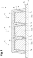
- FIG 1 is a sectional view of the scintillator panel according to this embodiment.
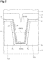
- FIG 2 is a schematic sectional view illustrating enlargement of a part of the scintillator panel illustrated in FIG. 1 . In FIG. 2 , hatching of elements is not illustrated.
- the scintillator panel 1 includes a substrate 2, a scintillator layer 3, a first protective layer 4, a reflective layer 5, and a second protective layer 6.
- the substrate 2 includes a principal surface 2s.
- the substrate 2 has, for example, a rectangular plate shape.
- the substrate 2 may have, for example, transmittivity of scintillation light which is generated in the scintillator layer 3.
- the thickness of the substrate 2 is, for example, about 2.0 mm.
- the substrate 2 is formed of, for example, a fiber optic plate (FOP: an optical device formed by binding a plurality of optical fibers (for example, J5734 made by Hamamatsu Photonics K.K.)).
- FOP fiber optic plate
- the scintillator layer 3 generates scintillation light such as visible light in response to incidence of radiation R such as X-rays.
- the scintillator layer 3 is disposed on the principal surface 2s of the substrate 2.
- the scintillator layer 3 is formed in a rectangular area of the principal surface 2s when viewed from a direction crossing (for example, perpendicular to) the principal surface 2s.
- the scintillator layer 3 includes a plurality of scintillator portions 7.
- the scintillator portions 7 are arranged with a predetermined pitch in a two-dimensional shape on the principal surface 2s.
- the scintillator portions 7 are in contact with, for example, the principal surface 2s.
- the scintillator portions 7 are not continuously connected to each other (are separated from each other).
- the scintillator portions 7 are formed, for example, as pixel units of an imaging sensor (that is, the scintillator layer 3 is made into pixels).
- the sectional shape of each scintillator portion 7 is, for example, a trapezoidal shape which is reduced as it is farther from the principal surface 2s. That is, each scintillator portion 7 has a taper shape of which a sectional area increases from the opposite side of the principal surface 2s to the principal surface 2s.
- Each scintillator portion 7 is formed of, for example, a single crystal of a scintillator material.
- the scintillator portion 7 is formed of, for example, a plurality of columnar crystals of a scintillator material.
- the scintillator material include a material containing CsI (cesium iodide) such as CsI:Tl or CsI:Na as a main component, a material containing NaI (sodium iodide) such as NaI:Tl as a main component, SrI 3 (strontium iodide), LuI 3 (lutetium iodide), BaF 2 (barium fluoride), and GOS.
- Each scintillator portion 7 includes side faces 7s extending in a direction (for example, a growing direction of columnar crystals) crossing the principal surface 2s.
- the scintillator portion 7 also includes a top face 7t that extends in a direction parallel to the principal surface 2s.
- the top face 7t connects the side faces 7s.
- a height H of the scintillator portion 7 ranges, for example, from about 150 ⁇ m to 1000 ⁇ m.
- the height H of the scintillator portion 7 is a distance between the top face 7t and the principal surface 2s and a thickness of the scintillator layer 3.
- a gap G between the side faces 7s of the neighboring scintillator portions 7 is narrowed toward the principal surface 2s along the shape of the scintillator portions 7.
- an upper gap G1 on the top face 7t side ranges, for example, from about 5 ⁇ m to 50 ⁇ m.
- an intermediate gap G2 of an intermediate portion between the top face 7t and the principal surface 2s ranges, for example, from about 3 ⁇ m to 30 ⁇ m.
- a lower gap G3 on the principal surface 2s side ranges, for example, from about 2 ⁇ m to 15 ⁇ m.
- a processing pitch (for example, the predetermined pitch) of the scintillator layer 3 is, for example, about 200 ⁇ m.
- the processing pitch is a pitch of the gaps between the scintillator portions 7.
- the first protective layer 4 is disposed on the scintillator layer 3 and the principal surface 2s of the substrate 2.
- the first protective layer 4 transmits radiation R. More specifically, the first protective layer 4 is disposed so as to cover the surface (the side faces 7s and the top face 7t) of each scintillator portion 7 and the principal surface 2s which is exposed from the scintillator layer 3 between the scintillator portions 7.
- the first protective layer 4 prevents an organic solvent from invading between columnar crystals of the scintillator portions 7.
- a thickness T of the first protective layer 4 ranges, for example, from 1 ⁇ m to 10 ⁇ m.
- the first protective layer 4 is formed of, for example, parylene (polyparaxylene).
- the reflective layer 5 is disposed on the scintillator layer 3 and the first protective layer 4. More specifically, the reflective layer 5 is disposed on the scintillator portions 7 with the first protective layer 4 interposed therebetween so as to cover the entire surface (the side faces 7s and the top face 7t) of each scintillator portion 7.
- the reflective layer 5 reflects scintillation light which is generated in the scintillator layer 3.
- the reflective layer 5 transmits radiation R.
- the reflective layer 5 includes a plurality of metal particles 8. Accordingly, the metal particles 8 reflect scintillation light and transmits radiation R.
- the metal particles 8 are disposed on the surface (the side faces 7s and the top face 7t) of each scintillator portion 7.
- the metal particles 8 have a foil shape (for example, a scale shape, a flake shape, or a leaf shape) that extends along the surface of the scintillator portion 7. That is, on the side faces 7s of the scintillator portion 7, the metal particles 8 extend along the side faces 7s (are arranged along the side faces 7s).
- the metal particles 8 overlap other metal particles 8 at least partially and come into contact therewith. Accordingly, the metal particles 8 cover the whole surface of the scintillator portion 7 with no break.
- a metal particle 8 When a metal particle 8 has a foil shape, it means that the metal particle 8 does not have a spherical shape or a needle shape. More specifically, when a metal particle 8 has a foil shape, it means that, for example, when the metal particle 8 is disposed on the side face 7s, a size (a width) of the metal particle 8 along the side face 7s is larger than a size (a thickness) of the metal particle 8 in a direction crossing the side face 7s.
- the average size of the metal particles 8 ranges, for example, from about 1 ⁇ m to 20 ⁇ m and may range from about 3 ⁇ m to 10 ⁇ m.
- the average size of the metal particles 8 can be set, for example, to be equal to or less than half the gap G (particularly the upper gap G1) between the side faces 7s of the neighboring scintillator portions 7.
- the average size of the metal particles 8 may be set to be equal to or less than half a value which is obtained by subtracting two times the thickness of the first protective layer 4 from the gap G.
- the average size of the metal particles 8 is, for example, a size which is obtained by averaging a maximum size of the metal particles 8 for a plurality of metal particles 8.
- the metal particles 8 are formed of, for example, Al, Ag, Au, or Pt.
- a particle size distribution of the metal particles 8 can be defined, for example, by a median diameter (d50) or an arithmetic average value (sum of diameters of particles/number of particles).
- the second protective layer 6 is disposed on the reflective layer 5. More specifically, the second protective layer 6 is formed on the reflective layer 5 so as to cover the scintillator layer 3, the first protective layer 4, and the reflective layer 5 as a whole.
- the second protective layer 6 transmits radiation R.
- the second protective layer 6 is formed, for example, of parylene (polyparaxylene).
- a scintillator layer is formed on the principal surface 2s by causing columnar crystals of a scintillation material to grow on the principal surface 2s of the substrate 2, for example, by a vacuum vapor deposition method.
- the scintillator layer is processed such that the scintillator layer is cut into a plurality of parts (the scintillator layer is made into pixels), for example, by irradiation with a laser beam.
- the scintillator layer 3 including a plurality of scintillator portions 7 is formed on the principal surface 2s.
- the first protective layer 4 is formed on the scintillator layer 3 and the principal surface 2s. More specifically, the first protective layer 4 is formed so as to cover the surface (the side faces 7s and the top face 7t) of each scintillator portion 7 and the principal surface 2s which is exposed between the scintillator portions 7. Accordingly, in a subsequent step, an organic solvent is prevented from invading between the columnar crystals of the scintillator layer 3. It is possible to prevent the metal particles 8 from coming in direct contact with the scintillator layer 3. Through the above-mentioned steps, a scintillator panel including the substrate 2, the scintillator layer 3, and the first protective layer 4 is obtained.
- the scintillator panel obtained through the above-mentioned steps is put in a vacuum vessel.
- a metal paste including the metal particles 8 is applied onto the first protective layer 4.
- the metal paste may not fill the gaps between the side faces 7s of the scintillator portions 7.
- the metal paste is cured, for example, by performing cold curing, thermal curing, or UV curing.
- the reflective layer 5 is formed so as to cover the scintillator layer 3 with the first protective layer 4 interposed therebetween.
- the second protective layer 6 is formed on the reflective layer 5. More specifically, in this step, the second protective layer 6 is formed on the reflective layer 5 to cover the scintillator layer 3, the first protective layer 4, and the reflective layer 5 as a whole. Accordingly, it is possible to protect the reflective layer 5 and to improve moisture resistance of the scintillator layer 3. Through the above-mentioned steps, the scintillator panel 1 is manufactured.
- the metal paste can be manufactured, for example, as follows. That is, first, a metal powder (such as metal foils), an organic solvent, and a pulverization aid are mixed using a ball mill (a spread pulverization step). Subsequently, the mixture is sieved with a sieve (a sieving step). Through this step, metal particles 8 of which the average size has been controlled are obtained. Subsequently, the mixture is separated into a solid (the metal particles 8) and a liquid (a filtration step). Then, the metal particles 8, an organic solvent, and a binder resin are mixed. As a result, the metal paste is manufactured.
- FIG 3 is a photograph illustrating an example of the reflective layer of the scintillator panel illustrated in FIG. 1 .
- the scintillator layer 3 includes a plurality of scintillator portions 7 which are arranged with a predetermined pitch on the principal surface 2s of the substrate 2.
- the reflective layer 5 that reflects scintillation light is provided so as to cover at least the side faces 7s of the scintillator portions 7.
- the reflective layer 5 includes a plurality of foil-shaped metal particles 8 that extend along the side faces 7s of the scintillator portions 7.
- an absorber layer for example, an absorber layer including carbon black
- a light output may decrease in comparison with a case in which the absorber layer is not formed.
- the scintillator panel 1 it is possible to curb a decrease in a light output and to improve a resolution by using the reflective layer 5 including the foil-shaped metal particles 8.
- the surface (the side faces 7s and the top faces 7t) of the scintillator layer 3 can be covered with a plurality of metal particles 8 as a whole with no break (that is, a continuous reflective surface can be formed) by causing the foil-shaped metal particles 8 that reflect scintillation light to at least partially overlap, as illustrated in FIGS. 2 and 3 .
- FIG 4 is a graph illustrating an evaluation result of a resolution (MTF) and a light output of the scintillator panel.
- "WITH REFLECTIVE LAYER” corresponds to an example of the scintillator panel 1.
- CsI:Tl is used as the scintillation material of the scintillator layer 3
- the thickness of the scintillator layer 3 (the height H of the scintillator portions 7) is set to 150 ⁇ m
- the processing depth of the scintillator layer 3 (the depth of the gap between the scintillator portions 7) is set to 150 ⁇ m
- the metal particles 8 of the reflective layer 5 are formed of Al.
- "WITH ABSORBER LAYER" in the graph illustrated in FIG. 4 corresponds to a scintillator panel according to a first comparative example.
- an absorber layer including carbon is provided instead of the reflective layer 5.
- "WITHOUT ABSORBER LAYER" in the graph illustrated in FIG. 4 corresponds to a scintillator panel according to a second comparative example.
- the reflective layer 5 and the absorber layer are not provided.
- values of resolutions and light outputs in the example and the first comparative example are illustrated relative to the values of the resolution and the light output (100%) in the second comparative example.
- the resolution is improved to 140% in comparison with the second comparative example of "WITHOUT REFLECTIVE LAYER,” but the light output is decreased to 30%.
- the resolution is improved to substantially the same degree as in the first comparative example in comparison with the second comparative example and the decrease of the light output is curbed in comparison with the first comparative example. From this evaluation result, it can be seen that the scintillator panel 1 can curb a decrease of a light output and improve a resolution.
- the average size of the metal particles 8 is equal to or less than half the gap G between the side faces 7s of the neighboring scintillator portions 7. Accordingly, when the reflective layer 5 is formed, the metal particles 8 can be disposed so as to cover the side faces 7s of the scintillator portions 7 by easily and reliably entering the foil-shaped metal particles 8 to the gaps between the side faces 7s of the scintillator portions 7. Accordingly, it is possible to reliably curb a decrease in a light output and to further improve a resolution.
- the first protective layer 4 is formed on the scintillator layer 3. Accordingly, when the reflective layer 5 is formed, it is possible to prevent an organic solvent included in the metal paste from entering between the columnar crystals of the scintillator portions 7. Since the scintillator layer 3 does not come in direct contact with the metal particles 8, it is possible to prevent a reaction between the scintillator material and the metal from giving an adverse influence.
- a scintillator panel according to an aspect of the invention is not limited to the scintillator panel 1.
- the scintillator panel 1 can be arbitrarily modified or can be applied to another device without departing from the gist of the appended claims.
- FIG. 5 is a sectional view of a scintillator panel according to a modified example.
- a scintillator panel 1A is different from the scintillator panel 1 in that a scintillator layer 3A is provided instead of the scintillator layer 3.
- the scintillator layer 3A generates scintillation light such as visible light in response to incidence of radiation R such as X-rays.
- the scintillator layer 3A is formed on the principal surface 2s of the substrate 2.
- the scintillator layer 3A is formed in a rectangular area of the principal surface 2s when viewed in a direction crossing (for example, perpendicular to) the principal surface 2s.
- the scintillator layer 3A includes a single base portion 71 and a plurality of scintillator portions 72.
- the base portion 71 and the scintillator portions 72 are formed of, for example, a single crystal of a scintillation material.
- the base portion 71 and the scintillator portions 72 are formed of, for example, a plurality of columnar crystals of a scintillation material.
- the scintillation material is the same as described above.
- the base portion 71 is formed on the principal surface 2s.
- the base portion 71 extends along the principal surface 2s.
- the scintillator portions 72 are two-dimensionally arranged on the principal surface 2s and the base portion 71.
- the scintillator portions 72 are not directly connected to each other.
- the scintillator portions 72 are formed, for example, in pixel units of an imaging sensor (that is, the scintillator layer 3A is partitioned into pixels).
- the scintillator portions 72 are connected to each other via the base portion 71.
- the base portion 71 connects the scintillator portions 72.
- each scintillator portion 72 is, for example, a trapezoidal shape that reduces away from the principal surface 2s and the base portion 71. That is, each scintillator portion 72 is a taper shape in which a sectional area increases from the opposite side of the principal surface 2s and the base portion 71 to the principal surface 2s and the base portion 71.
- Each scintillator portion 72 includes side faces 72s that extend in a direction crossing the principal surface 2s (for example, a direction in which columnar crystals grow).
- Each scintillator portion 72 includes a top face 72t that extends in a direction parallel to the principal surface 2s. The top face 72t connects the side faces 72s.
- a relationship between the sizes of parts of the scintillator layer 3A and the average size of the metal particles 8 can be defined in the same range as in the scintillator panel 1.
- the thickness of the scintillator layer 3A (the sum of the height of the base portion 71 and the height of the scintillator portions 72) can be set to about 600 ⁇ m.
- the processing depth of the scintillator layer 3A (the depth of the gaps between the scintillator portions 72) can be set to, for example, 300 ⁇ m.
- the height of the base portion 71 and the height of the scintillator portions 72 are both about 300 ⁇ m.
- Such a scintillator layer 3A can be manufactured, for example, by forming grooves in the scintillator layer with a processing depth not reaching the principal surface 2s at the time of laser processing of the scintillator layer in the method of manufacturing the scintillator panel 1. With the scintillator panel 1A, the same advantages as in the scintillator panel 1 can be achieved.
- FIG 6 is a sectional view of a scintillator panel according to another modified example.
- a scintillator panel 1B is different from the scintillator panel 1 in that a scintillator layer 3B is provided instead of the scintillator layer 3.
- the scintillator layer 3B generates scintillation light such as visible light in response to incidence of radiation R such as X-rays.
- the scintillator layer 3B is formed on the principal surface 2s of the substrate 2.
- the scintillator layer 3B is formed in a rectangular area of the principal surface 2s when viewed in a direction crossing (for example, perpendicular to) the principal surface 2s.
- the scintillator layer 3B includes a plurality of scintillator portions 73.
- the scintillator portions 73 are formed of, for example, a single crystal of a scintillation material.
- the scintillator portions 73 are formed of, for example, a plurality of columnar crystals of a scintillation material.
- the scintillation material is the same as described above.
- the scintillator portions 73 are two-dimensionally arranged with a predetermined pitch on the principal surface 2s.
- the scintillator portions 73 are not connected to each other. In other words, the scintillator portions 73 arc formed, for example, in pixel units of an imaging sensor (that is, the scintillator layer 3A is partitioned into pixels).
- a sectional shape of each scintillator portion 73 is a rectangular shape. That is, the scintillator portions 73 do not substantially have taper shapes in comparison with the scintillator portions 7.
- Each scintillator portion 73 includes side faces 73s that extend in a direction crossing the principal surface 2s (for example, a direction in which columnar crystals grow).
- Each scintillator portion 73 includes a top face 73t that extends in a direction parallel to the principal surface 2s.
- the top face 73t connects the side faces 73s.
- the side faces 73s which are arranged along one of two-dimensional arrangement directions of the scintillator portions 73 are substantially parallel to each other.
- a relationship between the sizes of parts of the scintillator layer 3B and the average size of the metal particles 8 can be defined in the same range as in the scintillator panel 1.
- the gap G between the side faces 73s is substantially constant in a direction from the top face 73t to the principal surface 2s.
- the first protective layer 4, the reflective layer 5, and the second protective layer 6 are formed to follow the rectangular shapes of the scintillator portions 73.
- Such a scintillator layer 3B can be manufactured, for example, by controlling processing conditions and the like such that the rectangular scintillator portions 73 are formed at the time of laser processing of the scintillator layer in the method of manufacturing the scintillator panel 1. With the scintillator panel 1B, the same advantages as in the scintillator panel 1 can be achieved.
- each scintillator portion 72 may be set to a rectangular shape.
- a scintillator panel for example, the scintillator panels 1, 1A, and 1B
- a sensor panel for example, a TFT panel or a CMOS image sensor panel
- photoelectric conversion elements can be used as a substrate to construct a radiation detector.
- a radiation detector according to an embodiment will be described below.
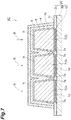
- FIG. 7 is a sectional view of a radiation detector according to the embodiment.
- a radiation detector 1C is different from the scintillator panel 1 in that a substrate 2C serving as a sensor panel is provided instead of the substrate 2.
- the substrate (the sensor panel) 2C includes a principal surface 2s and a plurality of photoelectric conversion elements 10 formed on the principal surface 2s. More specifically, the substrate 2C includes a panel-shaped base portion 2p including the principal surface 2s.
- the photoelectric conversion elements 10 are arranged two-dimensionally on the principal surface 2s.
- a scintillator layer 3 is formed on the principal surface 2s and the photoelectric conversion elements 10, for example, by vapor deposition.
- a film portion 11 such as a passivation film or a planarization film is formed on the principal surface 2s and the photoelectric conversion elements 10.
- the scintillator layer 3 is formed on the principal surface 2s and the photoelectric conversion elements 10 with the film portion 11 interposed therebetween.
- the scintillator layer 3 is optically coupled to the photoelectric conversion elements 10. More specifically, in the scintillator layer 3, one scintillator portion 7 is provided so as to correspond to one photoelectric conversion element 10.
- the scintillator portions 7 are two-dimensionally arranged such that they are located on the photoelectric conversion elements 10 when viewed in a direction crossing the principal surface 2s. Accordingly, the scintillator portions 7 are arranged with a pixel pitch of the photoelectric conversion elements 10. Accordingly, the scintillator portions 7 are optically coupled to the photoelectric conversion elements 10 respectively.
- the photoelectric conversion elements 10 receive scintillation light which is generated from the scintillator layer 3 (the respective scintillator portions 7) in response to incidence of radiation R and output an electrical signal corresponding to the scintillation light.
- the electrical signal is externally extracted by a wire or the like which is not illustrated. Accordingly, the radiation detector 1C detects radiation R.
- the scintillator layer 3 includes a plurality of scintillator portions 7 which are arranged with the pixel pitch of the photoelectric conversion elements 10 on the substrate 2C.
- a reflective layer 5 that reflects scintillation light is disposed so as to cover at least the side faces 7s of the scintillator portions 7.
- the reflective layer 5 includes a plurality of foil-shaped metal particles 8 that extend along the side faces 7s of the scintillator portions 7. In this way, by using the reflective layer 5 including the foil-shaped metal particles 8, it is possible to curb a decrease in a light output and to improve a resolution.
- the average size of the metal particles 8 is equal to or less than half the gap G between the side faces 7s of the neighboring scintillator portions 7. Accordingly, when the reflective layer 5 is formed, the foil-shaped metal particles 8 can easily and satisfactorily enter the gaps between the side faces 7s of the scintillator portions 7 and the metal particles 8 can be arranged to cover the side faces 7s of the scintillator portions 7. Accordingly, it is possible to satisfactorily curb a decrease in a light output and to further improve a resolution.
- a first protective layer 4 is formed on the scintillator layer 3. Accordingly, when the reflective layer 5 is formed, it is possible to prevent an organic solvent included in a metal paste from invading between the columnar crystals of the scintillator portions 7. Since the scintillator layer 3 and the metal particles 8 do not come into direct contact with each other, it is possible to prevent a reaction between the scintillation material and metal from giving an adverse influence.
- the radiation detector 1C can achieve the following different advantages. That is, the radiation detector 1C is constructed by forming the scintillator layer 3 directly on the substrate 2C (and the film portion 11) serving as a sensor panel, for example, by vapor deposition. Accordingly, when the radiation detector is constructed, it is not necessary to bond a sensor panel and a scintillator panel, which are prepared as independent members, to each other. In the scintillator panels 1, 1A, and 1B, a sensor panel may be separately provided on the rear surface of the substrate 2 opposite to the principal surface 2s to construct a radiation detector.
- the radiation detector 1C is constructed by replacing the substrate 2 of the scintillator panel 1 with the substrate 2C including the photoelectric conversion elements 10.
- the substrate 2 of the scintillator panels 1A and 1B may be replaced with the substrate 2C including the photoelectric conversion elements 10 to construct a radiation detector.
Landscapes
- Health & Medical Sciences (AREA)
- Life Sciences & Earth Sciences (AREA)
- High Energy & Nuclear Physics (AREA)
- Physics & Mathematics (AREA)
- Molecular Biology (AREA)
- Engineering & Computer Science (AREA)
- General Physics & Mathematics (AREA)
- Spectroscopy & Molecular Physics (AREA)
- Medical Informatics (AREA)
- General Engineering & Computer Science (AREA)
- Biomedical Technology (AREA)
- Surgery (AREA)
- Chemical & Material Sciences (AREA)
- Nuclear Medicine, Radiotherapy & Molecular Imaging (AREA)
- Optics & Photonics (AREA)
- Pathology (AREA)
- Radiology & Medical Imaging (AREA)
- Crystallography & Structural Chemistry (AREA)
- Biophysics (AREA)
- Animal Behavior & Ethology (AREA)
- Heart & Thoracic Surgery (AREA)
- General Health & Medical Sciences (AREA)
- Public Health (AREA)
- Veterinary Medicine (AREA)
- Measurement Of Radiation (AREA)
- Conversion Of X-Rays Into Visible Images (AREA)
- Apparatus For Radiation Diagnosis (AREA)
Abstract
Description
- An aspect of the invention relates to a scintillator panel and a radiation detector.
-
Patent Literature 1 discloses an X-ray flat panel detector. The X-ray flat panel detector includes a plurality of pixel units which are two-dimensionally arranged. Each pixel unit includes a scintillator portion. A cutoff area is formed between the scintillator portions of pixel units adjacent to each other. A reflective member that reflects visible light is disposed in the cutoff area. - Patent Literature 1: Japanese Unexamined Patent Publication No.
2003-167060 - In such an X-ray flat panel detector, an improvement in resolution is achieved using an X-ray absorbing material as a material of the reflective member. In this way, there is demand for an improvement in resolution in this technical field. In order to improve a resolution, for example, disposing an absorber layer that absorbs scintillation light in the cutoff area can be considered. However, in this case, there is concern of a decrease of a light output.
- An object of an aspect of the invention is to provide a scintillator panel and a radiation detector that can curb a decrease of a light output and improve a resolution.
- According to an aspect of the invention, there is provided a scintillator panel that converts radiation into scintillation light, the scintillator panel including: a substrate that includes a principal surface; a scintillator layer that is disposed with a predetermined pitch on the principal surface; and a reflective layer that is disposed on the scintillator layer and reflects the scintillation light, wherein the scintillator layer includes a plurality of scintillator portions which are arranged on the principal surface, each scintillator portion includes a side face that extends in a direction crossing the principal surface, and the reflective layer includes a plurality of metal particles with a foil shape extending along the side faces and is disposed so as to cover the side faces.
- In the scintillator panel, the scintillator layer includes a plurality of scintillator portions that are arranged with a predetermined pitch on the principal surface of the substrate. The reflective layer that reflects scintillation light is disposed so as to cover at least the side faces of the scintillator portions. The reflective layer includes a plurality of metal particles with a foil shape extending along the side faces of the scintillator portions. By using the reflective layer including metal particles with a foil shape in this way, it is possible to curb a decrease of a light output and to improve a resolution.
- In the scintillator panel according to an aspect of the invention, an average size of the metal particles may be equal to or less than half a gap size between the side faces of the neighboring scintillator portions. In this case, the reflective layer can be formed such that the side faces of the scintillator portions are covered by easily and reliably entering the metal particles with a foil shape to the gaps between the side faces of the scintillator portions. Accordingly, it is possible to reliably curb a decrease of a light output and to improve a resolution. The average size of the metal particles with a foil shape is, for example, a value which is obtained by averaging a maximum size of a metal particle for the plurality of metal particles.
- In the scintillator panel according to an aspect of the invention, the scintillator layer may be formed of a scintillator material containing CsI as a main component. In the scintillator panel according to an aspect of the invention, each scintillator portion may be formed of a single crystal of a scintillator material. Alternatively, in the scintillator panel according to an aspect of the invention, each scintillator portion may be formed of a plurality of columnar crystals of a scintillator material.
- According to an aspect of the invention, there is provided a radiation detector including: a substrate that includes a principal surface and a plurality of photoelectric conversion elements formed on the principal surface; a scintillator layer that is disposed on the plurality of photoelectric conversion elements and converts radiation into scintillation light; and a reflective layer that is disposed on the scintillator layer and reflects the scintillation light, wherein the scintillator layer includes a plurality of scintillator portions which are arranged with a pixel pitch of the photoelectric conversion elements, each scintillator portion includes a side face that extends in a direction crossing the principal surface, and the reflective layer includes a plurality of metal particles with a foil shape extending along the side faces and is disposed so as to cover the side faces.
- In the radiation detector, the scintillator layer includes a plurality of scintillator portions that are arranged with a pixel pitch of the photoelectric conversion elements of the substrate. The reflective layer that reflects scintillation light is disposed to cover at least the side faces of the scintillator portions. The reflective layer includes a plurality of metal particles with a foil shape that extend along the side faces of the scintillator portions. By using the reflective layer including metal particles with a foil shape in this way, it is possible to curb a decrease of a light output and to improve a resolution.
- In the radiation detector according to an aspect of the invention, an average size of the metal particles may be equal to or less than half a gap size between the side faces of the neighboring scintillator portions. In this case, the reflective layer can be formed such that the side faces of the scintillator portions are covered by easily and reliably entering the metal particles with a foil shape to the gaps between the side faces of the scintillator portions. Accordingly, it is possible to reliably curb a decrease of a light output and to improve a resolution.
- In the radiation detector according to an aspect of the invention, the scintillator layer may be formed of a scintillator material containing CsI as a main component. In the radiation detector according to an aspect of the invention, each scintillator portion may be formed of a single crystal of a scintillator material. Alternatively, in the radiation detector according to an aspect of the invention, each scintillator portion may be formed of a plurality of columnar crystals of a scintillator material. The scintillator layer may be formed of a scintillator material which is GOS.
- According to an aspect of the invention, it is possible to provide a scintillator panel and a radiation detector that can curb a decrease of a light output and improve a resolution.
-
-
FIG 1 is a sectional view of a scintillator panel according to an embodiment of the invention. -
FIG. 2 is a schematic sectional view illustrating enlargement of a part of the scintillator panel illustrated inFIG. 1 . -
FIG. 3 is a photograph illustrating an example of a reflective layer of the scintillator panel illustrated inFIG. 1 . -
FIG 4 is a graph illustrating an evaluation result of a resolution and a light output of the scintillator panel. -
FIG 5 is a sectional view of a scintillator panel according to a modified example. -
FIG. 6 is a sectional view of a scintillator panel according to another modified example. -
FIG 7 is a sectional view of a radiation detector according to the embodiment. - Hereinafter, an embodiment of an aspect of the invention will be described in detail with reference to the accompanying drawings. In the drawings, the same or corresponding elements will be referenced by the same reference signs and description thereof may not be repeated.
- A scintillator panel according to an embodiment serves to convert radiation such as X-rays into scintillation light such as visible light. The scintillator panel according to the following embodiment can be used, for example, as a radiological imaging device in a mammography device, a mass chest diagnostic device, a CT device, a dental intraoral imaging device, a radiological camera, or the like.
-
FIG 1 is a sectional view of the scintillator panel according to this embodiment.FIG 2 is a schematic sectional view illustrating enlargement of a part of the scintillator panel illustrated inFIG. 1 . InFIG. 2 , hatching of elements is not illustrated. As illustrated inFIGS. 1 and2 , thescintillator panel 1 includes asubstrate 2, ascintillator layer 3, a firstprotective layer 4, areflective layer 5, and a secondprotective layer 6. - The
substrate 2 includes aprincipal surface 2s. Thesubstrate 2 has, for example, a rectangular plate shape. Thesubstrate 2 may have, for example, transmittivity of scintillation light which is generated in thescintillator layer 3. The thickness of thesubstrate 2 is, for example, about 2.0 mm. Thesubstrate 2 is formed of, for example, a fiber optic plate (FOP: an optical device formed by binding a plurality of optical fibers (for example, J5734 made by Hamamatsu Photonics K.K.)). - The
scintillator layer 3 generates scintillation light such as visible light in response to incidence of radiation R such as X-rays. Thescintillator layer 3 is disposed on theprincipal surface 2s of thesubstrate 2. For example, thescintillator layer 3 is formed in a rectangular area of theprincipal surface 2s when viewed from a direction crossing (for example, perpendicular to) theprincipal surface 2s. - The
scintillator layer 3 includes a plurality ofscintillator portions 7. Thescintillator portions 7 are arranged with a predetermined pitch in a two-dimensional shape on theprincipal surface 2s. Thescintillator portions 7 are in contact with, for example, theprincipal surface 2s. For example, thescintillator portions 7 are not continuously connected to each other (are separated from each other). In other words, thescintillator portions 7 are formed, for example, as pixel units of an imaging sensor (that is, thescintillator layer 3 is made into pixels). The sectional shape of eachscintillator portion 7 is, for example, a trapezoidal shape which is reduced as it is farther from theprincipal surface 2s. That is, eachscintillator portion 7 has a taper shape of which a sectional area increases from the opposite side of theprincipal surface 2s to theprincipal surface 2s. - Each
scintillator portion 7 is formed of, for example, a single crystal of a scintillator material. Alternatively, thescintillator portion 7 is formed of, for example, a plurality of columnar crystals of a scintillator material. Examples of the scintillator material include a material containing CsI (cesium iodide) such as CsI:Tl or CsI:Na as a main component, a material containing NaI (sodium iodide) such as NaI:Tl as a main component, SrI3 (strontium iodide), LuI3 (lutetium iodide), BaF2 (barium fluoride), and GOS. - Each
scintillator portion 7 includes side faces 7s extending in a direction (for example, a growing direction of columnar crystals) crossing theprincipal surface 2s. Thescintillator portion 7 also includes atop face 7t that extends in a direction parallel to theprincipal surface 2s. Thetop face 7t connects the side faces 7s. A height H of thescintillator portion 7 ranges, for example, from about 150 µm to 1000 µm. The height H of thescintillator portion 7 is a distance between thetop face 7t and theprincipal surface 2s and a thickness of thescintillator layer 3. - A gap G between the side faces 7s of the neighboring
scintillator portions 7 is narrowed toward theprincipal surface 2s along the shape of thescintillator portions 7. In the gap G, an upper gap G1 on thetop face 7t side ranges, for example, from about 5 µm to 50 µm. In the gap G, an intermediate gap G2 of an intermediate portion between thetop face 7t and theprincipal surface 2s ranges, for example, from about 3 µm to 30 µm. In the gap G, a lower gap G3 on theprincipal surface 2s side ranges, for example, from about 2 µm to 15 µm. A processing pitch (for example, the predetermined pitch) of thescintillator layer 3 is, for example, about 200 µm. The processing pitch is a pitch of the gaps between thescintillator portions 7. - The first
protective layer 4 is disposed on thescintillator layer 3 and theprincipal surface 2s of thesubstrate 2. The firstprotective layer 4 transmits radiation R. More specifically, the firstprotective layer 4 is disposed so as to cover the surface (the side faces 7s and thetop face 7t) of eachscintillator portion 7 and theprincipal surface 2s which is exposed from thescintillator layer 3 between thescintillator portions 7. For example, the firstprotective layer 4 prevents an organic solvent from invading between columnar crystals of thescintillator portions 7. A thickness T of the firstprotective layer 4 ranges, for example, from 1 µm to 10 µm. The firstprotective layer 4 is formed of, for example, parylene (polyparaxylene). - The
reflective layer 5 is disposed on thescintillator layer 3 and the firstprotective layer 4. More specifically, thereflective layer 5 is disposed on thescintillator portions 7 with the firstprotective layer 4 interposed therebetween so as to cover the entire surface (the side faces 7s and thetop face 7t) of eachscintillator portion 7. Thereflective layer 5 reflects scintillation light which is generated in thescintillator layer 3. Thereflective layer 5 transmits radiation R. Thereflective layer 5 includes a plurality ofmetal particles 8. Accordingly, themetal particles 8 reflect scintillation light and transmits radiation R. - The
metal particles 8 are disposed on the surface (the side faces 7s and thetop face 7t) of eachscintillator portion 7. Themetal particles 8 have a foil shape (for example, a scale shape, a flake shape, or a leaf shape) that extends along the surface of thescintillator portion 7. That is, on the side faces 7s of thescintillator portion 7, themetal particles 8 extend along the side faces 7s (are arranged along the side faces 7s). Themetal particles 8 overlapother metal particles 8 at least partially and come into contact therewith. Accordingly, themetal particles 8 cover the whole surface of thescintillator portion 7 with no break. - When a
metal particle 8 has a foil shape, it means that themetal particle 8 does not have a spherical shape or a needle shape. More specifically, when ametal particle 8 has a foil shape, it means that, for example, when themetal particle 8 is disposed on theside face 7s, a size (a width) of themetal particle 8 along theside face 7s is larger than a size (a thickness) of themetal particle 8 in a direction crossing theside face 7s. - The average size of the
metal particles 8 ranges, for example, from about 1 µm to 20 µm and may range from about 3 µm to 10 µm. Particularly, the average size of themetal particles 8 can be set, for example, to be equal to or less than half the gap G (particularly the upper gap G1) between the side faces 7s of the neighboringscintillator portions 7. When the firstprotective layer 4 is formed on the side faces 7s, the average size of themetal particles 8 may be set to be equal to or less than half a value which is obtained by subtracting two times the thickness of the firstprotective layer 4 from the gap G. - The average size of the
metal particles 8 is, for example, a size which is obtained by averaging a maximum size of themetal particles 8 for a plurality ofmetal particles 8. Themetal particles 8 are formed of, for example, Al, Ag, Au, or Pt. A particle size distribution of themetal particles 8 can be defined, for example, by a median diameter (d50) or an arithmetic average value (sum of diameters of particles/number of particles). - The second
protective layer 6 is disposed on thereflective layer 5. More specifically, the secondprotective layer 6 is formed on thereflective layer 5 so as to cover thescintillator layer 3, the firstprotective layer 4, and thereflective layer 5 as a whole. The secondprotective layer 6 transmits radiation R. The secondprotective layer 6 is formed, for example, of parylene (polyparaxylene). - An example of a method of manufacturing the
scintillator panel 1 will be described below. In the manufacturing method, first, a scintillator layer is formed on theprincipal surface 2s by causing columnar crystals of a scintillation material to grow on theprincipal surface 2s of thesubstrate 2, for example, by a vacuum vapor deposition method. Subsequently, the scintillator layer is processed such that the scintillator layer is cut into a plurality of parts (the scintillator layer is made into pixels), for example, by irradiation with a laser beam. Accordingly, thescintillator layer 3 including a plurality ofscintillator portions 7 is formed on theprincipal surface 2s. - Subsequently, the first
protective layer 4 is formed on thescintillator layer 3 and theprincipal surface 2s. More specifically, the firstprotective layer 4 is formed so as to cover the surface (the side faces 7s and thetop face 7t) of eachscintillator portion 7 and theprincipal surface 2s which is exposed between thescintillator portions 7. Accordingly, in a subsequent step, an organic solvent is prevented from invading between the columnar crystals of thescintillator layer 3. It is possible to prevent themetal particles 8 from coming in direct contact with thescintillator layer 3. Through the above-mentioned steps, a scintillator panel including thesubstrate 2, thescintillator layer 3, and the firstprotective layer 4 is obtained. - Subsequently, the scintillator panel obtained through the above-mentioned steps is put in a vacuum vessel. In a state in which the vacuum vessel is evacuated into a vacuum, a metal paste including the
metal particles 8 is applied onto the firstprotective layer 4. At this time, the metal paste may not fill the gaps between the side faces 7s of thescintillator portions 7. Thereafter, by opening the vacuum vessel to the atmospheric air, the gaps are filled with the metal paste using a pressure difference between the gaps between the side faces 7s and the atmospheric air. After the metal paste has been filled, the metal paste is cured, for example, by performing cold curing, thermal curing, or UV curing. By this step, thereflective layer 5 is formed so as to cover thescintillator layer 3 with the firstprotective layer 4 interposed therebetween. - Subsequently, the second
protective layer 6 is formed on thereflective layer 5. More specifically, in this step, the secondprotective layer 6 is formed on thereflective layer 5 to cover thescintillator layer 3, the firstprotective layer 4, and thereflective layer 5 as a whole. Accordingly, it is possible to protect thereflective layer 5 and to improve moisture resistance of thescintillator layer 3. Through the above-mentioned steps, thescintillator panel 1 is manufactured. - The metal paste can be manufactured, for example, as follows. That is, first, a metal powder (such as metal foils), an organic solvent, and a pulverization aid are mixed using a ball mill (a spread pulverization step). Subsequently, the mixture is sieved with a sieve (a sieving step). Through this step,
metal particles 8 of which the average size has been controlled are obtained. Subsequently, the mixture is separated into a solid (the metal particles 8) and a liquid (a filtration step). Then, themetal particles 8, an organic solvent, and a binder resin are mixed. As a result, the metal paste is manufactured. - Advantages which are achieved by the
scintillator panel 1 will be described below with reference toFIGS. 1 to 4 .FIG 3 is a photograph illustrating an example of the reflective layer of the scintillator panel illustrated inFIG. 1 . In thescintillator panel 1, thescintillator layer 3 includes a plurality ofscintillator portions 7 which are arranged with a predetermined pitch on theprincipal surface 2s of thesubstrate 2. Thereflective layer 5 that reflects scintillation light is provided so as to cover at least the side faces 7s of thescintillator portions 7. Thereflective layer 5 includes a plurality of foil-shapedmetal particles 8 that extend along the side faces 7s of thescintillator portions 7. - For example, when an absorber layer (for example, an absorber layer including carbon black) that absorbs scintillation light is formed on the
scintillator layer 3, an improvement of a resolution is expected but a light output may decrease in comparison with a case in which the absorber layer is not formed. On the other hand, with thescintillator panel 1, it is possible to curb a decrease in a light output and to improve a resolution by using thereflective layer 5 including the foil-shapedmetal particles 8. This is because the surface (the side faces 7s and the top faces 7t) of thescintillator layer 3 can be covered with a plurality ofmetal particles 8 as a whole with no break (that is, a continuous reflective surface can be formed) by causing the foil-shapedmetal particles 8 that reflect scintillation light to at least partially overlap, as illustrated inFIGS. 2 and3 . - For example, when a reflective layer including spherical metal particles is formed, an improvement in a resolution may not be expected. The reason thereof is considered as follows. That is, it is difficult to cover the side faces 7s in a fine gap between the side faces 7s of the
scintillator portions 7 with the spherical metal particles with no break. Accordingly, it is difficult to prevent transmission of scintillation light and to reduce crosstalk. -
FIG 4 is a graph illustrating an evaluation result of a resolution (MTF) and a light output of the scintillator panel. In the graph illustrated inFIG. 4 , "WITH REFLECTIVE LAYER" corresponds to an example of thescintillator panel 1. In the example of thescintillator panel 1, CsI:Tl is used as the scintillation material of thescintillator layer 3, the thickness of the scintillator layer 3 (the height H of the scintillator portions 7) is set to 150 µm, the processing depth of the scintillator layer 3 (the depth of the gap between the scintillator portions 7) is set to 150 µm, and themetal particles 8 of thereflective layer 5 are formed of Al. - "WITH ABSORBER LAYER" in the graph illustrated in
FIG. 4 corresponds to a scintillator panel according to a first comparative example. In the first comparative example, an absorber layer including carbon is provided instead of thereflective layer 5. "WITHOUT ABSORBER LAYER" in the graph illustrated inFIG. 4 corresponds to a scintillator panel according to a second comparative example. In the second comparative example, thereflective layer 5 and the absorber layer are not provided. In the graph illustrated inFIG. 4 , values of resolutions and light outputs in the example and the first comparative example are illustrated relative to the values of the resolution and the light output (100%) in the second comparative example. - As illustrated in
FIG. 4 , according to the first comparative example of "WITH ABSORBER LAYER," the resolution is improved to 140% in comparison with the second comparative example of "WITHOUT REFLECTIVE LAYER," but the light output is decreased to 30%. On the other hand, according to the example, the resolution is improved to substantially the same degree as in the first comparative example in comparison with the second comparative example and the decrease of the light output is curbed in comparison with the first comparative example. From this evaluation result, it can be seen that thescintillator panel 1 can curb a decrease of a light output and improve a resolution. - Advantages which are achieved by the
scintillator panel 1 will be described below. In thescintillator panel 1, the average size of themetal particles 8 is equal to or less than half the gap G between the side faces 7s of the neighboringscintillator portions 7. Accordingly, when thereflective layer 5 is formed, themetal particles 8 can be disposed so as to cover the side faces 7s of thescintillator portions 7 by easily and reliably entering the foil-shapedmetal particles 8 to the gaps between the side faces 7s of thescintillator portions 7. Accordingly, it is possible to reliably curb a decrease in a light output and to further improve a resolution. - In the
scintillator panel 1, the firstprotective layer 4 is formed on thescintillator layer 3. Accordingly, when thereflective layer 5 is formed, it is possible to prevent an organic solvent included in the metal paste from entering between the columnar crystals of thescintillator portions 7. Since thescintillator layer 3 does not come in direct contact with themetal particles 8, it is possible to prevent a reaction between the scintillator material and the metal from giving an adverse influence. - An example of the scintillator panel according to an aspect of the invention has been described above. Accordingly, a scintillator panel according to an aspect of the invention is not limited to the
scintillator panel 1. As the scintillator panel according to an aspect of the invention, thescintillator panel 1 can be arbitrarily modified or can be applied to another device without departing from the gist of the appended claims. -
FIG. 5 is a sectional view of a scintillator panel according to a modified example. As illustrated inFIG. 5 , ascintillator panel 1A is different from thescintillator panel 1 in that ascintillator layer 3A is provided instead of thescintillator layer 3. Thescintillator layer 3A generates scintillation light such as visible light in response to incidence of radiation R such as X-rays. Thescintillator layer 3A is formed on theprincipal surface 2s of thesubstrate 2. For example, thescintillator layer 3A is formed in a rectangular area of theprincipal surface 2s when viewed in a direction crossing (for example, perpendicular to) theprincipal surface 2s. - The
scintillator layer 3A includes asingle base portion 71 and a plurality ofscintillator portions 72. Thebase portion 71 and thescintillator portions 72 are formed of, for example, a single crystal of a scintillation material. Alternatively, thebase portion 71 and thescintillator portions 72 are formed of, for example, a plurality of columnar crystals of a scintillation material. The scintillation material is the same as described above. - The
base portion 71 is formed on theprincipal surface 2s. Thebase portion 71 extends along theprincipal surface 2s. For example, thebase portion 71 comes in contact with theprincipal surface 2s. Thescintillator portions 72 are two-dimensionally arranged on theprincipal surface 2s and thebase portion 71. Thescintillator portions 72 are not directly connected to each other. In other words, thescintillator portions 72 are formed, for example, in pixel units of an imaging sensor (that is, thescintillator layer 3A is partitioned into pixels). Thescintillator portions 72 are connected to each other via thebase portion 71. In other words, thebase portion 71 connects thescintillator portions 72. - A sectional shape of each
scintillator portion 72 is, for example, a trapezoidal shape that reduces away from theprincipal surface 2s and thebase portion 71. That is, eachscintillator portion 72 is a taper shape in which a sectional area increases from the opposite side of theprincipal surface 2s and thebase portion 71 to theprincipal surface 2s and thebase portion 71. Eachscintillator portion 72 includes side faces 72s that extend in a direction crossing theprincipal surface 2s (for example, a direction in which columnar crystals grow). Eachscintillator portion 72 includes atop face 72t that extends in a direction parallel to theprincipal surface 2s. Thetop face 72t connects the side faces 72s. - A relationship between the sizes of parts of the
scintillator layer 3A and the average size of themetal particles 8 can be defined in the same range as in thescintillator panel 1. For example, the thickness of thescintillator layer 3A (the sum of the height of thebase portion 71 and the height of the scintillator portions 72) can be set to about 600 µm. The processing depth of thescintillator layer 3A (the depth of the gaps between the scintillator portions 72) can be set to, for example, 300 µm. In this case, the height of thebase portion 71 and the height of thescintillator portions 72 are both about 300 µm. - Such a
scintillator layer 3A can be manufactured, for example, by forming grooves in the scintillator layer with a processing depth not reaching theprincipal surface 2s at the time of laser processing of the scintillator layer in the method of manufacturing thescintillator panel 1. With thescintillator panel 1A, the same advantages as in thescintillator panel 1 can be achieved. -
FIG 6 is a sectional view of a scintillator panel according to another modified example. As illustrated inFIG. 6 , ascintillator panel 1B is different from thescintillator panel 1 in that ascintillator layer 3B is provided instead of thescintillator layer 3. Thescintillator layer 3B generates scintillation light such as visible light in response to incidence of radiation R such as X-rays. Thescintillator layer 3B is formed on theprincipal surface 2s of thesubstrate 2. For example, thescintillator layer 3B is formed in a rectangular area of theprincipal surface 2s when viewed in a direction crossing (for example, perpendicular to) theprincipal surface 2s. - The
scintillator layer 3B includes a plurality ofscintillator portions 73. Thescintillator portions 73 are formed of, for example, a single crystal of a scintillation material. Alternatively, thescintillator portions 73 are formed of, for example, a plurality of columnar crystals of a scintillation material. The scintillation material is the same as described above. Thescintillator portions 73 are two-dimensionally arranged with a predetermined pitch on theprincipal surface 2s. Thescintillator portions 73 are not connected to each other. In other words, thescintillator portions 73 arc formed, for example, in pixel units of an imaging sensor (that is, thescintillator layer 3A is partitioned into pixels). - A sectional shape of each
scintillator portion 73 is a rectangular shape. That is, thescintillator portions 73 do not substantially have taper shapes in comparison with thescintillator portions 7. Eachscintillator portion 73 includes side faces 73s that extend in a direction crossing theprincipal surface 2s (for example, a direction in which columnar crystals grow). Eachscintillator portion 73 includes atop face 73t that extends in a direction parallel to theprincipal surface 2s. Thetop face 73t connects the side faces 73s. The side faces 73s which are arranged along one of two-dimensional arrangement directions of thescintillator portions 73 are substantially parallel to each other. - A relationship between the sizes of parts of the
scintillator layer 3B and the average size of themetal particles 8 can be defined in the same range as in thescintillator panel 1. In thescintillator layer 3B, since the neighboring side faces 73s in one direction are substantially parallel to each other, the gap G between the side faces 73s is substantially constant in a direction from thetop face 73t to theprincipal surface 2s. In thescintillator panel 1B, the firstprotective layer 4, thereflective layer 5, and the secondprotective layer 6 are formed to follow the rectangular shapes of thescintillator portions 73. - Such a
scintillator layer 3B can be manufactured, for example, by controlling processing conditions and the like such that therectangular scintillator portions 73 are formed at the time of laser processing of the scintillator layer in the method of manufacturing thescintillator panel 1. With thescintillator panel 1B, the same advantages as in thescintillator panel 1 can be achieved. - In the
scintillator panel 1A illustrated inFIG. 5 , the sectional shape of eachscintillator portion 72 may be set to a rectangular shape. - In the above-mentioned embodiment, an example in which an aspect of the invention is applied to a scintillator panel (for example, the
scintillator panels -
FIG. 7 is a sectional view of a radiation detector according to the embodiment. As illustrated inFIG. 7 , aradiation detector 1C is different from thescintillator panel 1 in that a substrate 2C serving as a sensor panel is provided instead of thesubstrate 2. The substrate (the sensor panel) 2C includes aprincipal surface 2s and a plurality ofphotoelectric conversion elements 10 formed on theprincipal surface 2s. More specifically, the substrate 2C includes a panel-shapedbase portion 2p including theprincipal surface 2s. Thephotoelectric conversion elements 10 are arranged two-dimensionally on theprincipal surface 2s. - A
scintillator layer 3 is formed on theprincipal surface 2s and thephotoelectric conversion elements 10, for example, by vapor deposition. Here, afilm portion 11 such as a passivation film or a planarization film is formed on theprincipal surface 2s and thephotoelectric conversion elements 10. Thescintillator layer 3 is formed on theprincipal surface 2s and thephotoelectric conversion elements 10 with thefilm portion 11 interposed therebetween. Thescintillator layer 3 is optically coupled to thephotoelectric conversion elements 10. More specifically, in thescintillator layer 3, onescintillator portion 7 is provided so as to correspond to onephotoelectric conversion element 10. That is, thescintillator portions 7 are two-dimensionally arranged such that they are located on thephotoelectric conversion elements 10 when viewed in a direction crossing theprincipal surface 2s. Accordingly, thescintillator portions 7 are arranged with a pixel pitch of thephotoelectric conversion elements 10. Accordingly, thescintillator portions 7 are optically coupled to thephotoelectric conversion elements 10 respectively. - Accordingly, the
photoelectric conversion elements 10 receive scintillation light which is generated from the scintillator layer 3 (the respective scintillator portions 7) in response to incidence of radiation R and output an electrical signal corresponding to the scintillation light. The electrical signal is externally extracted by a wire or the like which is not illustrated. Accordingly, theradiation detector 1C detects radiation R. - The
radiation detector 1C achieves at least the same advantages as in the above-mentioned scintillator panel. More specifically, in theradiation detector 1C, thescintillator layer 3 includes a plurality ofscintillator portions 7 which are arranged with the pixel pitch of thephotoelectric conversion elements 10 on the substrate 2C. Areflective layer 5 that reflects scintillation light is disposed so as to cover at least the side faces 7s of thescintillator portions 7. Thereflective layer 5 includes a plurality of foil-shapedmetal particles 8 that extend along the side faces 7s of thescintillator portions 7. In this way, by using thereflective layer 5 including the foil-shapedmetal particles 8, it is possible to curb a decrease in a light output and to improve a resolution. - In the
radiation detector 1C, the average size of themetal particles 8 is equal to or less than half the gap G between the side faces 7s of the neighboringscintillator portions 7. Accordingly, when thereflective layer 5 is formed, the foil-shapedmetal particles 8 can easily and satisfactorily enter the gaps between the side faces 7s of thescintillator portions 7 and themetal particles 8 can be arranged to cover the side faces 7s of thescintillator portions 7. Accordingly, it is possible to satisfactorily curb a decrease in a light output and to further improve a resolution. - In the
radiation detector 1C, a firstprotective layer 4 is formed on thescintillator layer 3. Accordingly, when thereflective layer 5 is formed, it is possible to prevent an organic solvent included in a metal paste from invading between the columnar crystals of thescintillator portions 7. Since thescintillator layer 3 and themetal particles 8 do not come into direct contact with each other, it is possible to prevent a reaction between the scintillation material and metal from giving an adverse influence. - The
radiation detector 1C can achieve the following different advantages. That is, theradiation detector 1C is constructed by forming thescintillator layer 3 directly on the substrate 2C (and the film portion 11) serving as a sensor panel, for example, by vapor deposition. Accordingly, when the radiation detector is constructed, it is not necessary to bond a sensor panel and a scintillator panel, which are prepared as independent members, to each other. In thescintillator panels substrate 2 opposite to theprincipal surface 2s to construct a radiation detector. - In the above description, the
radiation detector 1C is constructed by replacing thesubstrate 2 of thescintillator panel 1 with the substrate 2C including thephotoelectric conversion elements 10. However, thesubstrate 2 of thescintillator panels photoelectric conversion elements 10 to construct a radiation detector. - It is possible to provide a scintillator panel and a radiation detector that can curb a decrease of a light output and improve a resolution.
- 1, 1A, 1B... scintillator panel, 1C... radiation detector, 2, 2C... substrate, 2s... principal surface, 3, 3A, 3B... scintillator layer, 5... reflective layer, 7, 72, 73... scintillator portion, 7s, 72s, 73s... side face, 8... metal particle, 10... photoelectric conversion element, G... gap, R... radiation
Claims (12)
- A scintillator panel that converts radiation into scintillation light, the scintillator panel comprising:a substrate that includes a principal surface;a scintillator layer that is disposed on the principal surface; anda reflective layer that is disposed on the scintillator layer and reflects the scintillation light,wherein the scintillator layer includes a plurality of scintillator portions which are arranged with a predetermined pitch on the principal surface,wherein each scintillator portion includes a side face that extends in a direction crossing the principal surface, andwherein the reflective layer includes a plurality of metal particles with a foil shape extending along the side faces and is disposed so as to cover the side faces.
- The scintillator panel according to claim 1, wherein an average size of the metal particles is equal to or less than half a gap size between the side faces of the neighboring scintillator portions.
- The scintillator panel according to claim 1 or 2, wherein the scintillator layer is formed of a scintillator material containing CsI as a main component.
- The scintillator panel according to claim 1 or 2, wherein the scintillator layer is formed of a scintillator material which is GOS.
- The scintillator panel according to any one of claims 1 to 4, wherein each scintillator portion is formed of a single crystal of a scintillator material.
- The scintillator panel according to any one of claims 1 to 4, wherein each scintillator portion is formed of a plurality of columnar crystals of a scintillator material.
- A radiation detector comprising:a substrate that includes a principal surface and a plurality of photoelectric conversion elements formed on the principal surface;a scintillator layer that is disposed on the plurality of photoelectric conversion elements and converts radiation into scintillation light; anda reflective layer that is disposed on the scintillator layer and reflects the scintillation light,wherein the scintillator layer includes a plurality of scintillator portions which are arranged with a pixel pitch of the photoelectric conversion elements,wherein each scintillator portion includes a side face that extends in a direction crossing the principal surface, andwherein the reflective layer includes a plurality of metal particles with a foil shape extending along the side faces and is disposed so as to cover the side faces.
- The radiation detector according to claim 7, wherein an average size of the metal particles is equal to or less than half a gap size between the side faces of the neighboring scintillator portions.
- The radiation detector according to claim 7 or 8, wherein the scintillator layer is formed of a scintillator material containing CsI as a main component.
- The radiation detector according to claim 7 or 8, wherein the scintillator layer is formed of a scintillator material which is GOS.
- The radiation detector according to any one of claims 7 to 10, wherein each scintillator portion is formed of a single crystal of a scintillator material.
- The radiation detector according to any one of claims 7 to 10, wherein each scintillator portion is formed of a plurality of columnar crystals of a scintillator material.
Applications Claiming Priority (2)
| Application Number | Priority Date | Filing Date | Title |
|---|---|---|---|
| JP2015243188A JP6548565B2 (en) | 2015-12-14 | 2015-12-14 | Scintillator panel and radiation detector |
| PCT/JP2016/085342 WO2017104400A1 (en) | 2015-12-14 | 2016-11-29 | Scintillator panel and radiation detector |
Publications (3)
| Publication Number | Publication Date |
|---|---|
| EP3392678A1 true EP3392678A1 (en) | 2018-10-24 |
| EP3392678A4 EP3392678A4 (en) | 2019-07-31 |
| EP3392678B1 EP3392678B1 (en) | 2022-06-22 |
Family
ID=59056070
Family Applications (1)
| Application Number | Title | Priority Date | Filing Date |
|---|---|---|---|
| EP16875384.6A Active EP3392678B1 (en) | 2015-12-14 | 2016-11-29 | Scintillator panel and radiation detector |
Country Status (6)
| Country | Link |
|---|---|
| US (1) | US10302776B2 (en) |
| EP (1) | EP3392678B1 (en) |
| JP (1) | JP6548565B2 (en) |
| KR (1) | KR20180092938A (en) |
| CN (1) | CN108369283A (en) |
| WO (1) | WO2017104400A1 (en) |
Families Citing this family (5)
| Publication number | Priority date | Publication date | Assignee | Title |
|---|---|---|---|---|
| JP6701288B2 (en) | 2018-09-06 | 2020-05-27 | キヤノン株式会社 | Scintillator plate, radiation detector and radiation detection system |
| KR102634270B1 (en) * | 2018-11-27 | 2024-02-06 | 한국전기연구원 | Intra-oral Radiation Detector of Low-dose and High resolution |
| JP7470631B2 (en) * | 2020-12-23 | 2024-04-18 | 浜松ホトニクス株式会社 | Radiation detector, method for manufacturing radiation detector, and scintillator panel unit |
| JP7587980B2 (en) * | 2020-12-23 | 2024-11-21 | 浜松ホトニクス株式会社 | Radiation detector, method for manufacturing radiation detector, and scintillator panel unit |
| JP7608148B2 (en) * | 2020-12-23 | 2025-01-06 | 浜松ホトニクス株式会社 | Radiation detector, method for manufacturing radiation detector, and scintillator panel unit |
Family Cites Families (29)
| Publication number | Priority date | Publication date | Assignee | Title |
|---|---|---|---|---|
| JPH10319126A (en) | 1997-05-16 | 1998-12-04 | S I I R D Center:Kk | Radiation detector and its manufacturing method |
| JP2002107457A (en) * | 2000-10-02 | 2002-04-10 | Canon Inc | Phosphor structure, radiation imaging apparatus having the same, and radiation imaging system |
| JP2003167060A (en) | 2001-11-30 | 2003-06-13 | Toshiba Corp | X-ray flat panel detector |
| JP4300453B2 (en) * | 2002-06-28 | 2009-07-22 | Dic株式会社 | Reversible thermosensitive magnetic information recording medium with improved light reflecting layer |
| US8068896B2 (en) * | 2005-02-25 | 2011-11-29 | Intramedical Imaging, Llc | Detection of radiation labeled sites using a radiation detection probe or camera incorporating a solid state photo-multiplier |
| US7358506B2 (en) * | 2005-12-15 | 2008-04-15 | Palo Alto Research Center Incorporated | Structured X-ray conversion screen fabricated with molded layers |
| JP4192990B2 (en) * | 2006-03-13 | 2008-12-10 | 日立金属株式会社 | Radiation detector |
| EP2118684A2 (en) * | 2007-03-05 | 2009-11-18 | Koninklijke Philips Electronics N.V. | Improved light detection in a pixelated pet detector |
| CN102239425B (en) * | 2008-12-23 | 2014-02-26 | 圣戈本陶瓷及塑料股份有限公司 | scintillation separator |
| WO2010092869A1 (en) * | 2009-02-12 | 2010-08-19 | 日立金属株式会社 | Radiation detector and method for manufacturing radiation detector |
| JP2012002627A (en) * | 2010-06-16 | 2012-01-05 | Konica Minolta Medical & Graphic Inc | Two-dimensional array scintillator for radiation detection |
| JP5911274B2 (en) * | 2011-11-28 | 2016-04-27 | キヤノン株式会社 | Radiation detection apparatus and radiation imaging system |
| EP2793052B1 (en) | 2011-12-01 | 2020-08-26 | Kabushiki Kaisha Toshiba | Scintillator array, and x-ray detector and x-ray examination device using scintillator array |
| JP2013228366A (en) * | 2012-03-29 | 2013-11-07 | Canon Inc | Radiation detector and radiation detection system |
| JP6071041B2 (en) * | 2012-03-30 | 2017-02-01 | 日立金属株式会社 | Manufacturing method of scintillator array and manufacturing method of radiation detector |
| JP6041594B2 (en) * | 2012-09-14 | 2016-12-14 | 浜松ホトニクス株式会社 | Scintillator panel and radiation detector |
| US9564253B2 (en) * | 2012-11-16 | 2017-02-07 | Toray Industries, Inc. | Scintillator panel |
| US9632185B2 (en) * | 2012-11-26 | 2017-04-25 | Toray Industries, Inc. | Scintillator panel and method for manufacturing the same |
| JP2015061041A (en) * | 2013-09-20 | 2015-03-30 | 株式会社東芝 | Radiation detector and radiation detection apparatus |
| JP6256042B2 (en) * | 2014-01-23 | 2018-01-10 | コニカミノルタ株式会社 | Radiation imaging system |
| US9223033B2 (en) * | 2014-02-26 | 2015-12-29 | Saint-Gobain Ceramics & Plastics, Inc. | Scintillator array and methods of forming a scintillator array and a radiation detector |
| JP5928848B2 (en) * | 2014-04-22 | 2016-06-01 | ウシオ電機株式会社 | Light irradiation device and long arc type discharge lamp |
| TWI550836B (en) * | 2014-05-06 | 2016-09-21 | 友達光電股份有限公司 | Photo detector and fabricating method thereof |
| JP6896425B2 (en) * | 2014-09-25 | 2021-06-30 | 株式会社東芝 | Scintillators, scintillator arrays, radiation detectors, and radiation inspection equipment |
| AU2014268284A1 (en) * | 2014-11-30 | 2016-06-16 | Southern Innovation International Pty Ltd | Method and apparatus for material identification |
| JP2016177009A (en) * | 2015-03-18 | 2016-10-06 | 東芝メディカルシステムズ株式会社 | Reflector, scintillator array, method for manufacturing scintillator array, and radiation detector |
| JP2016224105A (en) * | 2015-05-27 | 2016-12-28 | 株式会社東芝 | Optical reflection film, optical component using the same, and method of manufacturing optical reflection film |
| WO2017078051A1 (en) * | 2015-11-02 | 2017-05-11 | 株式会社 東芝 | Scintillator, scintillator array, radiation detector, and radiation examination device |
| JP6773683B2 (en) * | 2015-12-25 | 2020-10-21 | 株式会社東芝 | Ceramic scintillator array, X-ray detector, and X-ray inspection equipment |
-
2015
- 2015-12-14 JP JP2015243188A patent/JP6548565B2/en active Active
-
2016
- 2016-11-29 US US16/061,385 patent/US10302776B2/en active Active
- 2016-11-29 EP EP16875384.6A patent/EP3392678B1/en active Active
- 2016-11-29 CN CN201680073006.9A patent/CN108369283A/en active Pending
- 2016-11-29 WO PCT/JP2016/085342 patent/WO2017104400A1/en not_active Ceased
- 2016-11-29 KR KR1020187013222A patent/KR20180092938A/en not_active Withdrawn
Also Published As
| Publication number | Publication date |
|---|---|
| CN108369283A (en) | 2018-08-03 |
| US20190041532A1 (en) | 2019-02-07 |
| JP2017110929A (en) | 2017-06-22 |
| WO2017104400A1 (en) | 2017-06-22 |
| JP6548565B2 (en) | 2019-07-24 |
| KR20180092938A (en) | 2018-08-20 |
| EP3392678B1 (en) | 2022-06-22 |
| EP3392678A4 (en) | 2019-07-31 |
| US10302776B2 (en) | 2019-05-28 |
Similar Documents
| Publication | Publication Date | Title |
|---|---|---|
| EP3392678B1 (en) | Scintillator panel and radiation detector | |
| EP2128651A1 (en) | Radiation detector | |
| US9304212B2 (en) | Scintillator panel and manufacturing method therefor and radiation detector and manufacturing method therefor | |
| CN104718463B (en) | Scintillator panel and radiation detector | |
| US9684083B2 (en) | X-ray detector panel | |
| EP3438705B1 (en) | Radiation detector and scintillator panel | |
| US9012859B2 (en) | Tiled X-ray imager panel and method of forming the same | |
| CN104769681A (en) | Scintillator panel and radiation detection device | |
| EP3032280A1 (en) | Radiation detection apparatus and radiation detection sheet | |
| US9006662B2 (en) | Radiological image detection device | |
| JP7516640B2 (en) | Ceramic scintillator array, and radiation detector and radiation inspection device using the same | |
| US10345456B2 (en) | Radiation detector and method for producing a radiation detector | |
| US20160274250A1 (en) | Radiation detection apparatus, radiation imaging system, and manufacturing method | |
| WO2017169048A1 (en) | Radiation detector manufacturing method | |
| KR20160021387A (en) | Scintillator panel and method of manufacturing the same | |
| JP6949479B2 (en) | Scintillator plate, radiation detector and radiation measurement system | |
| JP2009025258A (en) | Radiation detector | |
| JP7662865B2 (en) | Scintillator array, radiation detector, and radiation inspection device | |
| KR20200009931A (en) | Radiation Detector for Implementing Low Dose and High Resolution using Backside Light-Receiving Structure | |
| WO2018020555A1 (en) | Scintillator sensor substrate and method for producing scintillator sensor substrate | |
| KR20210081146A (en) | Curved Radiation Detector for Implementing Low Dose and High Resolution using Backside Light-Receiving Structure | |
| JP2012047557A (en) | Radiation detector | |
| JP5767765B2 (en) | High resolution phosphor screen and method for producing high resolution phosphor screen | |
| US20160079301A1 (en) | X-ray detector | |
| JP2016020820A (en) | Radiation detector and scintillator panel |
Legal Events
| Date | Code | Title | Description |
|---|---|---|---|
| STAA | Information on the status of an ep patent application or granted ep patent |
Free format text: STATUS: THE INTERNATIONAL PUBLICATION HAS BEEN MADE |
|
| PUAI | Public reference made under article 153(3) epc to a published international application that has entered the european phase |
Free format text: ORIGINAL CODE: 0009012 |
|
| STAA | Information on the status of an ep patent application or granted ep patent |
Free format text: STATUS: REQUEST FOR EXAMINATION WAS MADE |
|
| 17P | Request for examination filed |
Effective date: 20180712 |
|
| AK | Designated contracting states |
Kind code of ref document: A1 Designated state(s): AL AT BE BG CH CY CZ DE DK EE ES FI FR GB GR HR HU IE IS IT LI LT LU LV MC MK MT NL NO PL PT RO RS SE SI SK SM TR |
|
| AX | Request for extension of the european patent |
Extension state: BA ME |
|
| DAV | Request for validation of the european patent (deleted) | ||
| DAX | Request for extension of the european patent (deleted) | ||
| A4 | Supplementary search report drawn up and despatched |
Effective date: 20190702 |
|
| RIC1 | Information provided on ipc code assigned before grant |
Ipc: G21K 4/00 20060101ALI20190626BHEP Ipc: A61B 6/00 20060101ALI20190626BHEP Ipc: G01T 1/202 20060101ALI20190626BHEP Ipc: G01T 1/20 20060101AFI20190626BHEP |
|
| STAA | Information on the status of an ep patent application or granted ep patent |
Free format text: STATUS: EXAMINATION IS IN PROGRESS |
|
| 17Q | First examination report despatched |
Effective date: 20220118 |
|
| GRAP | Despatch of communication of intention to grant a patent |
Free format text: ORIGINAL CODE: EPIDOSNIGR1 |
|
| STAA | Information on the status of an ep patent application or granted ep patent |
Free format text: STATUS: GRANT OF PATENT IS INTENDED |
|
| INTG | Intention to grant announced |
Effective date: 20220318 |
|
| GRAS | Grant fee paid |
Free format text: ORIGINAL CODE: EPIDOSNIGR3 |
|
| GRAA | (expected) grant |
Free format text: ORIGINAL CODE: 0009210 |
|
| STAA | Information on the status of an ep patent application or granted ep patent |
Free format text: STATUS: THE PATENT HAS BEEN GRANTED |
|
| AK | Designated contracting states |
Kind code of ref document: B1 Designated state(s): AL AT BE BG CH CY CZ DE DK EE ES FI FR GB GR HR HU IE IS IT LI LT LU LV MC MK MT NL NO PL PT RO RS SE SI SK SM TR |
|
| REG | Reference to a national code |
Ref country code: GB Ref legal event code: FG4D |
|
| REG | Reference to a national code |
Ref country code: CH Ref legal event code: EP |
|
| REG | Reference to a national code |
Ref country code: DE Ref legal event code: R096 Ref document number: 602016073065 Country of ref document: DE |
|
| REG | Reference to a national code |
Ref country code: AT Ref legal event code: REF Ref document number: 1500119 Country of ref document: AT Kind code of ref document: T Effective date: 20220715 |
|
| REG | Reference to a national code |
Ref country code: IE Ref legal event code: FG4D |
|
| REG | Reference to a national code |
Ref country code: NL Ref legal event code: FP |
|
| REG | Reference to a national code |
Ref country code: SE Ref legal event code: TRGR |
|
| REG | Reference to a national code |
Ref country code: LT Ref legal event code: MG9D |
|
| PG25 | Lapsed in a contracting state [announced via postgrant information from national office to epo] |
Ref country code: NO Free format text: LAPSE BECAUSE OF FAILURE TO SUBMIT A TRANSLATION OF THE DESCRIPTION OR TO PAY THE FEE WITHIN THE PRESCRIBED TIME-LIMIT Effective date: 20220922 Ref country code: LT Free format text: LAPSE BECAUSE OF FAILURE TO SUBMIT A TRANSLATION OF THE DESCRIPTION OR TO PAY THE FEE WITHIN THE PRESCRIBED TIME-LIMIT Effective date: 20220622 Ref country code: HR Free format text: LAPSE BECAUSE OF FAILURE TO SUBMIT A TRANSLATION OF THE DESCRIPTION OR TO PAY THE FEE WITHIN THE PRESCRIBED TIME-LIMIT Effective date: 20220622 Ref country code: GR Free format text: LAPSE BECAUSE OF FAILURE TO SUBMIT A TRANSLATION OF THE DESCRIPTION OR TO PAY THE FEE WITHIN THE PRESCRIBED TIME-LIMIT Effective date: 20220923 Ref country code: FI Free format text: LAPSE BECAUSE OF FAILURE TO SUBMIT A TRANSLATION OF THE DESCRIPTION OR TO PAY THE FEE WITHIN THE PRESCRIBED TIME-LIMIT Effective date: 20220622 Ref country code: BG Free format text: LAPSE BECAUSE OF FAILURE TO SUBMIT A TRANSLATION OF THE DESCRIPTION OR TO PAY THE FEE WITHIN THE PRESCRIBED TIME-LIMIT Effective date: 20220922 |
|
| REG | Reference to a national code |
Ref country code: AT Ref legal event code: MK05 Ref document number: 1500119 Country of ref document: AT Kind code of ref document: T Effective date: 20220622 |
|
| PG25 | Lapsed in a contracting state [announced via postgrant information from national office to epo] |
Ref country code: RS Free format text: LAPSE BECAUSE OF FAILURE TO SUBMIT A TRANSLATION OF THE DESCRIPTION OR TO PAY THE FEE WITHIN THE PRESCRIBED TIME-LIMIT Effective date: 20220622 Ref country code: LV Free format text: LAPSE BECAUSE OF FAILURE TO SUBMIT A TRANSLATION OF THE DESCRIPTION OR TO PAY THE FEE WITHIN THE PRESCRIBED TIME-LIMIT Effective date: 20220622 |
|
| PG25 | Lapsed in a contracting state [announced via postgrant information from national office to epo] |
Ref country code: SM Free format text: LAPSE BECAUSE OF FAILURE TO SUBMIT A TRANSLATION OF THE DESCRIPTION OR TO PAY THE FEE WITHIN THE PRESCRIBED TIME-LIMIT Effective date: 20220622 Ref country code: SK Free format text: LAPSE BECAUSE OF FAILURE TO SUBMIT A TRANSLATION OF THE DESCRIPTION OR TO PAY THE FEE WITHIN THE PRESCRIBED TIME-LIMIT Effective date: 20220622 Ref country code: RO Free format text: LAPSE BECAUSE OF FAILURE TO SUBMIT A TRANSLATION OF THE DESCRIPTION OR TO PAY THE FEE WITHIN THE PRESCRIBED TIME-LIMIT Effective date: 20220622 Ref country code: PT Free format text: LAPSE BECAUSE OF FAILURE TO SUBMIT A TRANSLATION OF THE DESCRIPTION OR TO PAY THE FEE WITHIN THE PRESCRIBED TIME-LIMIT Effective date: 20221024 Ref country code: ES Free format text: LAPSE BECAUSE OF FAILURE TO SUBMIT A TRANSLATION OF THE DESCRIPTION OR TO PAY THE FEE WITHIN THE PRESCRIBED TIME-LIMIT Effective date: 20220622 Ref country code: EE Free format text: LAPSE BECAUSE OF FAILURE TO SUBMIT A TRANSLATION OF THE DESCRIPTION OR TO PAY THE FEE WITHIN THE PRESCRIBED TIME-LIMIT Effective date: 20220622 Ref country code: CZ Free format text: LAPSE BECAUSE OF FAILURE TO SUBMIT A TRANSLATION OF THE DESCRIPTION OR TO PAY THE FEE WITHIN THE PRESCRIBED TIME-LIMIT Effective date: 20220622 Ref country code: AT Free format text: LAPSE BECAUSE OF FAILURE TO SUBMIT A TRANSLATION OF THE DESCRIPTION OR TO PAY THE FEE WITHIN THE PRESCRIBED TIME-LIMIT Effective date: 20220622 |
|
| PG25 | Lapsed in a contracting state [announced via postgrant information from national office to epo] |
Ref country code: PL Free format text: LAPSE BECAUSE OF FAILURE TO SUBMIT A TRANSLATION OF THE DESCRIPTION OR TO PAY THE FEE WITHIN THE PRESCRIBED TIME-LIMIT Effective date: 20220622 Ref country code: IS Free format text: LAPSE BECAUSE OF FAILURE TO SUBMIT A TRANSLATION OF THE DESCRIPTION OR TO PAY THE FEE WITHIN THE PRESCRIBED TIME-LIMIT Effective date: 20221022 |
|
| REG | Reference to a national code |
Ref country code: DE Ref legal event code: R097 Ref document number: 602016073065 Country of ref document: DE |
|
| PG25 | Lapsed in a contracting state [announced via postgrant information from national office to epo] |
Ref country code: AL Free format text: LAPSE BECAUSE OF FAILURE TO SUBMIT A TRANSLATION OF THE DESCRIPTION OR TO PAY THE FEE WITHIN THE PRESCRIBED TIME-LIMIT Effective date: 20220622 |
|
| PG25 | Lapsed in a contracting state [announced via postgrant information from national office to epo] |
Ref country code: DK Free format text: LAPSE BECAUSE OF FAILURE TO SUBMIT A TRANSLATION OF THE DESCRIPTION OR TO PAY THE FEE WITHIN THE PRESCRIBED TIME-LIMIT Effective date: 20220622 |
|
| PLBE | No opposition filed within time limit |
Free format text: ORIGINAL CODE: 0009261 |
|
| STAA | Information on the status of an ep patent application or granted ep patent |
Free format text: STATUS: NO OPPOSITION FILED WITHIN TIME LIMIT |
|
| 26N | No opposition filed |
Effective date: 20230323 |
|
| REG | Reference to a national code |
Ref country code: DE Ref legal event code: R119 Ref document number: 602016073065 Country of ref document: DE |
|
| P01 | Opt-out of the competence of the unified patent court (upc) registered |
Effective date: 20230509 |
|
| PG25 | Lapsed in a contracting state [announced via postgrant information from national office to epo] |
Ref country code: MC Free format text: LAPSE BECAUSE OF FAILURE TO SUBMIT A TRANSLATION OF THE DESCRIPTION OR TO PAY THE FEE WITHIN THE PRESCRIBED TIME-LIMIT Effective date: 20220622 |
|
| REG | Reference to a national code |
Ref country code: CH Ref legal event code: PL |
|
| REG | Reference to a national code |
Ref country code: BE Ref legal event code: MM Effective date: 20221130 |
|
| PG25 | Lapsed in a contracting state [announced via postgrant information from national office to epo] |
Ref country code: LI Free format text: LAPSE BECAUSE OF NON-PAYMENT OF DUE FEES Effective date: 20221130 Ref country code: CH Free format text: LAPSE BECAUSE OF NON-PAYMENT OF DUE FEES Effective date: 20221130 |
|
| PG25 | Lapsed in a contracting state [announced via postgrant information from national office to epo] |
Ref country code: SI Free format text: LAPSE BECAUSE OF FAILURE TO SUBMIT A TRANSLATION OF THE DESCRIPTION OR TO PAY THE FEE WITHIN THE PRESCRIBED TIME-LIMIT Effective date: 20220622 Ref country code: LU Free format text: LAPSE BECAUSE OF NON-PAYMENT OF DUE FEES Effective date: 20221129 |
|
| PG25 | Lapsed in a contracting state [announced via postgrant information from national office to epo] |
Ref country code: IE Free format text: LAPSE BECAUSE OF NON-PAYMENT OF DUE FEES Effective date: 20221129 Ref country code: DE Free format text: LAPSE BECAUSE OF NON-PAYMENT OF DUE FEES Effective date: 20230601 |
|
| PG25 | Lapsed in a contracting state [announced via postgrant information from national office to epo] |
Ref country code: BE Free format text: LAPSE BECAUSE OF NON-PAYMENT OF DUE FEES Effective date: 20221130 |
|
| PG25 | Lapsed in a contracting state [announced via postgrant information from national office to epo] |
Ref country code: IT Free format text: LAPSE BECAUSE OF FAILURE TO SUBMIT A TRANSLATION OF THE DESCRIPTION OR TO PAY THE FEE WITHIN THE PRESCRIBED TIME-LIMIT Effective date: 20220622 |
|
| PG25 | Lapsed in a contracting state [announced via postgrant information from national office to epo] |
Ref country code: HU Free format text: LAPSE BECAUSE OF FAILURE TO SUBMIT A TRANSLATION OF THE DESCRIPTION OR TO PAY THE FEE WITHIN THE PRESCRIBED TIME-LIMIT; INVALID AB INITIO Effective date: 20161129 |
|
| PG25 | Lapsed in a contracting state [announced via postgrant information from national office to epo] |
Ref country code: CY Free format text: LAPSE BECAUSE OF FAILURE TO SUBMIT A TRANSLATION OF THE DESCRIPTION OR TO PAY THE FEE WITHIN THE PRESCRIBED TIME-LIMIT Effective date: 20220622 |
|
| PG25 | Lapsed in a contracting state [announced via postgrant information from national office to epo] |
Ref country code: MK Free format text: LAPSE BECAUSE OF FAILURE TO SUBMIT A TRANSLATION OF THE DESCRIPTION OR TO PAY THE FEE WITHIN THE PRESCRIBED TIME-LIMIT Effective date: 20220622 |
|
| PG25 | Lapsed in a contracting state [announced via postgrant information from national office to epo] |
Ref country code: MT Free format text: LAPSE BECAUSE OF FAILURE TO SUBMIT A TRANSLATION OF THE DESCRIPTION OR TO PAY THE FEE WITHIN THE PRESCRIBED TIME-LIMIT Effective date: 20220622 |
|
| PG25 | Lapsed in a contracting state [announced via postgrant information from national office to epo] |
Ref country code: BG Free format text: LAPSE BECAUSE OF FAILURE TO SUBMIT A TRANSLATION OF THE DESCRIPTION OR TO PAY THE FEE WITHIN THE PRESCRIBED TIME-LIMIT Effective date: 20220622 |
|
| PG25 | Lapsed in a contracting state [announced via postgrant information from national office to epo] |
Ref country code: BG Free format text: LAPSE BECAUSE OF FAILURE TO SUBMIT A TRANSLATION OF THE DESCRIPTION OR TO PAY THE FEE WITHIN THE PRESCRIBED TIME-LIMIT Effective date: 20220622 |
|
| PGFP | Annual fee paid to national office [announced via postgrant information from national office to epo] |
Ref country code: FR Payment date: 20250930 Year of fee payment: 10 |
|
| PGFP | Annual fee paid to national office [announced via postgrant information from national office to epo] |
Ref country code: NL Payment date: 20251003 Year of fee payment: 10 |
|
| PG25 | Lapsed in a contracting state [announced via postgrant information from national office to epo] |
Ref country code: TR Free format text: LAPSE BECAUSE OF FAILURE TO SUBMIT A TRANSLATION OF THE DESCRIPTION OR TO PAY THE FEE WITHIN THE PRESCRIBED TIME-LIMIT Effective date: 20220622 |
|
| PGFP | Annual fee paid to national office [announced via postgrant information from national office to epo] |
Ref country code: GB Payment date: 20251001 Year of fee payment: 10 |
|
| PGFP | Annual fee paid to national office [announced via postgrant information from national office to epo] |
Ref country code: SE Payment date: 20251001 Year of fee payment: 10 |