JP7516640B2 - Ceramic scintillator array, and radiation detector and radiation inspection device using the same - Google Patents
Ceramic scintillator array, and radiation detector and radiation inspection device using the same Download PDFInfo
- Publication number
- JP7516640B2 JP7516640B2 JP2023153674A JP2023153674A JP7516640B2 JP 7516640 B2 JP7516640 B2 JP 7516640B2 JP 2023153674 A JP2023153674 A JP 2023153674A JP 2023153674 A JP2023153674 A JP 2023153674A JP 7516640 B2 JP7516640 B2 JP 7516640B2
- Authority
- JP
- Japan
- Prior art keywords
- scintillator
- scintillator array
- reflective layer
- ceramic
- resin
- Prior art date
- Legal status (The legal status is an assumption and is not a legal conclusion. Google has not performed a legal analysis and makes no representation as to the accuracy of the status listed.)
- Active
Links
Images
Landscapes
- Conversion Of X-Rays Into Visible Images (AREA)
- Measurement Of Radiation (AREA)
- Apparatus For Radiation Diagnosis (AREA)
Description
本発明の実施形態は、セラミックシンチレータアレイとそれを用いた放射線検出器、および放射線検査装置に関する。 Embodiments of the present invention relate to a ceramic scintillator array, a radiation detector using the same, and a radiation inspection device.
医療診断や工業用非破壊検査等の分野においては、X線断層写真撮影装置(以下、X線CT装置と記す)のような放射線検査装置を用いた検査が行なわれている。X線CT装置は、扇状のファンビームX線を照射するX線管(X線源)と、多数のX線検出素子を備えるX線検出器とを、被検査体の断層面を中央として対向配置して構成される。X線CT装置においては、被検査体に対して回転させながらX線管からファンビームX線を照射し、被検査体を透過したX線吸収データをX線検出器で収集する。この後、X線吸収データをコンピュータで解析することによって、断層像が再生される。X線CT装置の放射線検出器には、固体シンチレータを用いた検出素子が広く使用されている。固体シンチレータを用いた検出素子を具備する放射線検出器では、検出素子を小型化してチャンネル数を増やすことが容易であることから、X線CT装置等の解像度をより一層高めることができる。 In the fields of medical diagnosis and industrial non-destructive testing, inspections are performed using radiation inspection devices such as X-ray tomography devices (hereinafter referred to as X-ray CT devices). X-ray CT devices are configured by arranging an X-ray tube (X-ray source) that irradiates a fan-shaped fan beam X-rays and an X-ray detector equipped with a large number of X-ray detection elements facing each other with the tomographic plane of the object being inspected at the center. In the X-ray CT device, the X-ray tube irradiates the object being inspected with a fan beam X-ray while rotating it, and the X-ray absorption data that passes through the object is collected by the X-ray detector. After this, the X-ray absorption data is analyzed by a computer to reconstruct a tomographic image. Detection elements using solid scintillators are widely used in radiation detectors of X-ray CT devices. In radiation detectors equipped with detection elements using solid scintillators, it is easy to miniaturize the detection elements and increase the number of channels, so the resolution of X-ray CT devices and the like can be further improved.
X線CT装置等の放射線検査装置は、医療用や工業用等の様々な分野に用いられている。X線CT装置としては、例えばフォトダイオード等の検出素子を縦横に2次元的に並べ、その上にシンチレータアレイを搭載したマルチスライス型の装置が知られている。マルチスライス型とすることによって、輪切り画像を重ねることができ、これによりCT画像を立体的に示すことができる。放射線検査装置に搭載される放射線検出器は、縦横複数列に並べられた検出素子を備え、検出素子1個ずつにシンチレータセグメントが設けられている。シンチレータセグメントに入射したX線が可視光に変換され、可視光を検出素子で電気信号に変換して画像化する。近年は、高解像度を得るために検出素子を小型化し、さらに隣り合う検出素子間のピッチを狭くしている。これらに伴って、シンチレータセグメントのサイズも小さくなっている。 Radiation inspection devices such as X-ray CT scanners are used in various fields such as medical and industrial applications. For example, a multi-slice type X-ray CT scanner is known, in which detector elements such as photodiodes are arranged two-dimensionally vertically and horizontally, and a scintillator array is mounted on top of the detector elements. The multi-slice type allows cross-sectional images to be superimposed, thereby allowing the CT image to be displayed three-dimensionally. The radiation detector mounted on the radiation inspection device has detector elements arranged vertically and horizontally in multiple rows, and each detector element is provided with a scintillator segment. X-rays incident on the scintillator segment are converted into visible light, and the detector elements convert the visible light into electrical signals to produce an image. In recent years, detector elements have been made smaller in size to obtain higher resolution, and the pitch between adjacent detector elements has been narrowed. Accordingly, the size of the scintillator segments has also been reduced.
上述したようなシンチレータセグメントに使用される各種のシンチレータ材料のうち、希土類酸硫化物系の蛍光体セラミックスは、発光効率が高く、シンチレータセグメントに使用するために好適な特性を有している。このため、シンチレータ材料である希土類酸硫化物系蛍光体セラミックスの焼結体(インゴット)から切り出し加工または溝切り加工等により加工されたセラミックシンチレータセグメントと、検出素子としてのフォトダイオードとを組み合せた放射線検出器が普及しつつある。 Of the various scintillator materials used in the scintillator segments described above, rare earth oxysulfide phosphor ceramics have high luminous efficiency and are suitable for use in scintillator segments. For this reason, radiation detectors that combine ceramic scintillator segments cut or grooved from sintered bodies (ingots) of rare earth oxysulfide phosphor ceramics, which are the scintillator material, with photodiodes as detection elements are becoming more widespread.
蛍光体セラミックスを用いたシンチレータとしては、例えばガドリニウム酸硫化物蛍光体の焼結体からなるセラミックシンチレータが知られている。セラミックシンチレータアレイは、例えば以下のようにして作製される。まず、シンチレータ材料である希土類酸硫化物系蛍光体粉末を適当な形状に成形し、これを焼結して焼結体(インゴット)とする。このシンチレータ材料の焼結体に切り出し加工または溝切り加工等の切断加工を施して、複数の検出素子に対応するシンチレータセグメントを形成する。さらに、これらシンチレータセグメント間に反射層を形成して一体化してシンチレータアレイを作製する。 As a scintillator using phosphor ceramics, for example, a ceramic scintillator made of a sintered body of gadolinium oxysulfide phosphor is known. A ceramic scintillator array is produced, for example, as follows. First, rare earth oxysulfide phosphor powder, which is the scintillator material, is formed into an appropriate shape and sintered to form a sintered body (ingot). This sintered body of scintillator material is cut by cutting or grooving, etc., to form scintillator segments corresponding to multiple detection elements. Furthermore, a reflective layer is formed between these scintillator segments and integrated to produce a scintillator array.
上述したようなセラミックシンチレータアレイを放射線検出器として使用する場合、セラミックシンチレータアレイの寸法精度がCT診断画像の解像度に影響する。さらに、X線CT装置に搭載される放射線検出器には最大50℃~60℃の温度が加わる。樹脂を含む反射層を有するシンチレータアレイにおいては、加温による反射層の膨張、および温度低下による収縮が発生し、隣接するシンチレータセグメント間で微小な寸法変化、すなわちセグメントのピッチずれ、シンチレータアレイの反りを主な要因とする外形寸法のバラツキ等が生まれてしまう。こうした反り、外形寸法のバラツキがあると、検出器であるダイオードアレイに貼り付けたとき、その間の接着層厚を不均一にし、放射線検出器の診断画像の解像度を悪化させる原因となる。放射線検出器の診断画像の高解像度化が進む中、反り、外形寸法のバラツキの少ないシンチレータアレイが求められている。さらに、放射線検出器の検出面積の微細化に伴ってシンチレータアレイとダイオードアレイ間の接着層の均一化が重要になってきている。 When the above-mentioned ceramic scintillator array is used as a radiation detector, the dimensional accuracy of the ceramic scintillator array affects the resolution of the CT diagnostic image. Furthermore, the radiation detector mounted on the X-ray CT device is subjected to a maximum temperature of 50°C to 60°C. In a scintillator array having a reflective layer containing resin, the reflective layer expands due to heating and contracts due to a decrease in temperature, resulting in minute dimensional changes between adjacent scintillator segments, i.e., segment pitch deviation and variation in external dimensions caused mainly by warping of the scintillator array. If such warping and variation in external dimensions exist, when the scintillator array is attached to the diode array, which is the detector, the thickness of the adhesive layer between them becomes uneven, causing a deterioration in the resolution of the diagnostic image of the radiation detector. As the resolution of diagnostic images of radiation detectors increases, there is a demand for scintillator arrays with less warping and variation in external dimensions. Furthermore, as the detection area of radiation detectors becomes finer, it is becoming increasingly important to make the adhesive layer between the scintillator array and the diode array uniform.
X線CTなどに用いられるシンチレータはX線によって生じた光を、反射層を利用し画素内に閉じ込めて、フォトダイオード側に効率的に取り出す構造となっている。シンチレータまたはシンチレータアレイの反りが大きい場合,フォトダイオードに貼った際にシンチレータとフォトダイオード間を満たす接着層の厚みが不均一になり,接着層が厚いところでは,隣接する画素に光が入り,画素情報が重なる、所謂クロストークが大きくなることで,X線の検出感度が不均一になる.また,接着層に気泡が入りやすく,シンチレータからの光が散乱するため,X線の検出感度が低下するという問題があった。 Scintillators used in X-ray CT scanners are designed to confine light generated by X-rays within pixels using a reflective layer, and efficiently extract it to the photodiode side. If the scintillator or scintillator array is significantly warped, the thickness of the adhesive layer that fills the gap between the scintillator and photodiode when it is attached to the photodiode becomes uneven, and where the adhesive layer is thick, light enters adjacent pixels, causing pixel information to overlap, resulting in increased crosstalk and uneven X-ray detection sensitivity. In addition, air bubbles are easily trapped in the adhesive layer, which scatters the light from the scintillator, causing the problem of reduced X-ray detection sensitivity.
特許文献1には、シンチレータセグメント間の反射層において、エポキシ樹脂に含まれる反射粒子の色を選択し、またエポキシ樹脂のガラス転移点が80℃以上の樹脂を組み合わせることにより、シンチレータセグメント間の光出力のばらつきまたひずみを抑制する技術が開示されている。
特許文献2には、反射粒子を含み反射層を形成する透明樹脂のガラス転移点が50℃以上であり、かつガラス転移点より高い温度における前記透明樹脂の熱膨張係数が3.5×10⁻⁵/℃以下であるシンチレータアレイが開示されている。一般に、透明樹脂の熱膨張係数はガラス転移点を境にして、大きく変化し、それに伴って起こる反りを、その条件設定により対策したものである。
また特許文献3には、やはりシンチレータアレイの反りを低減するため、複数のシンチレータセグメントを一体化するように、隣接するシンチレータセグメント間の反射層部の透明樹脂のガラス転移点を50℃以上とし、複数のシンチレータセグメントのX線が入射する面側に配置された第2の反射層の透明樹脂のガラス転移点を30℃以下とする構成のシンチレータアレイが開示されている。
特許文献1~3にかかる方法により、シンチレータアレイの反りはある程度改善されるものの、画質の向上要求に伴って、シンチレータアレイの微細化が志向されるようになり、反りに伴って起こるクロストークによる画質低下また検出感度の低下に対する対策がさらに求められるようになってきている。
Although the methods described in
本発明は、複数のシンチレータセグメントを一体化するように、隣接するシンチレータセグメント間の反射層部を有するシンチレータアレイに関するものである。セラミックシンチレータの各セグメントの側面を囲うように設けられた反射層はシンチレータの使用温度領域よりも低いガラス転移点をもつ樹脂を用いることでシンチレータ自体が曲がり,フォトダイオード表面に沿うように張り合わせることができ、接着層厚の均一化を図ることが出来る。 The present invention relates to a scintillator array having a reflective layer between adjacent scintillator segments to integrate the multiple scintillator segments. The reflective layer that surrounds the side of each segment of the ceramic scintillator is made of a resin with a glass transition point lower than the operating temperature range of the scintillator, which allows the scintillator itself to bend and be bonded to the surface of the photodiode, making it possible to make the adhesive layer thickness uniform.
X線CT装置に搭載されるシンチレータアレイは、使用時の温度が50℃前後である。シンチレータアレイの反射層に用いられるエポキシ樹脂などの透明樹脂は、ガラス転移点と呼ばれる温度で、その線膨張係数が大きく変化する。このためガラス転移点が使用温度に近いものを選択すると、使用温度の前後で線膨張係数の変化により剥がれなどを起こしやすく、ガラス転移点が使用温度よりも高い透明樹脂が選択される傾向があった。
本発明のシンチレータアレイは、種々の試行を通し、透明樹脂のガラス転移点が使用温度より低い温度範囲のものを、選択すると、シンチレータアレイの反りが発生したとしても、柔軟性から、検出器のフォトダーオードアレイに密着させることが出来、接着層を均一化できることを見出した。これによって画素間での光のクロストークを抑制でき、検出感度の低下を低減させられる利点がある。
The temperature of the scintillator array mounted in the X-ray CT scanner is around 50°C during use. The linear expansion coefficient of the transparent resin, such as epoxy resin, used in the reflective layer of the scintillator array changes significantly at a temperature called the glass transition point. For this reason, if a resin with a glass transition point close to the operating temperature is selected, peeling or other problems are likely to occur due to the change in the linear expansion coefficient around the operating temperature, so there has been a tendency to select a transparent resin with a glass transition point higher than the operating temperature.
Through various trials, it was found that by selecting a transparent resin whose glass transition point is in a temperature range lower than the operating temperature, the scintillator array of the present invention can be attached to the photodiode array of the detector due to its flexibility even if the scintillator array warps, and the adhesive layer can be made uniform. This has the advantage of suppressing optical crosstalk between pixels and reducing the decrease in detection sensitivity.
以下、本発明のセラミックシンチレータアレイ、放射線検出器、および放射線検査装置を実施するための形態について説明する。 Below, we will explain the embodiments for implementing the ceramic scintillator array, radiation detector, and radiation inspection device of the present invention.
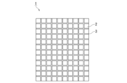
(セラミックシンチレータアレイ)
図1は実施形態のセラミックシンチレータアレイを示す平面図である。これらの図において、1はシンチレータアレイ、2はシンチレータセグメント、3は反射層である。シンチレータアレイ1は複数のシンチレータセグメント2を有している。隣接するシンチレータセグメント2間には、反射層3が介在している。反射層3は隣接するシンチレータセグメント2に対してそれぞれ接着されている。複数のシンチレータセグメント2は、それらに接着された反射層3で一体化されている。すなわち、シンチレータアレイ1は複数のシンチレータセグメント2を反射層3で一体化した構造を有している。また、個々のシンチレータセグメント全体を覆うように反射層が形成される場合もある(図1では省略されている)。
(Ceramic scintillator array)
Fig. 1 is a plan view showing a ceramic scintillator array of an embodiment. In these figures, 1 is a scintillator array, 2 is a scintillator segment, and 3 is a reflective layer. The
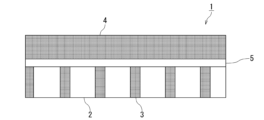
図2は本発明のシンチレータアレイの断面図を示したものである。図では、各シンチレータセグメント間に介在する反射層3とシンチレータアレイ全体を覆うように、X線入射側に配置された反射層4が示されている。反射層4は、反射粒子を含む透明樹脂を塗布、形成することが出来、または予め反射粒子を含む樹脂でシート状に成型されたものを、接着層5を介して、シンチレータアレイ上に付設することも出来る。X線入射側と反対側には、シンチレータによりX線から可視光に変換された光を検出するフォトダイオードアレイが張り合わされ、本発明の放射線検出器となる。
Figure 2 shows a cross-sectional view of the scintillator array of the present invention. The figure shows
シンチレータアレイ1は、複数のシンチレータセグメント2を一列に並べた構造、もしくは図1に示すように複数のシンチレータセグメント2を縦方向および横方向に所定の個数ずつ2次元的に並べた構造のいずれを有していてもよい。複数のシンチレータセグメント2を2次元的に配列した場合、縦方向および横方向のシンチレータセグメント2間にそれぞれ反射層3が設けられる。シンチレータセグメント2の個数は、X線検出器等の放射線検出器の構造や解像度等に応じて適宜設定される。
The
シンチレータセグメント2は、希土類酸硫化物蛍光体の焼結体からなるものである。希土類酸硫化物蛍光体セラミックスとしては、付活剤としてプラセオジム(Pr)を含有する希土類酸硫化物蛍光体が例示される。蛍光体セラミックスを構成する希土類酸硫化物としては、例えばイットリウム(Y)、ガドリニウム(Gd)、ランタン(La)、ルテチウム(Lu)等の希土類元素の酸硫化物が挙げられる。
The
実施形態のセラミックシンチレータアレイ1において、シンチレータセグメント2は、
一般式:RE2O2S:Pr …(1)
(式中、REはY、Gd、La、およびLuからなる群より選ばれる少なくとも1つの元素を示す)
で表される組成を有する希土類酸硫化物蛍光体セラミックス(シンチレータ材料)で構成されることが好ましい。
In the
General formula: RE2O2S : Pr...(1)
(In the formula, RE represents at least one element selected from the group consisting of Y, Gd, La, and Lu).
It is preferable that the scintillator material is a rare earth oxysulfide phosphor ceramic (scintillator material) having a composition represented by the following formula:
上述した希土類元素のうち、特にGdはX線吸収係数が大きく、セラミックシンチレータアレイ1の光出力の向上に寄与する。従って、実施形態のシンチレータセグメント2には、Gd2O2S:Pr(以後GOSとも略記される)蛍光体を使用することがさらに好ましい。なお、Gdの一部は他の希土類元素で置換してもよい。この際、他の希土類元素によるGdの置換量は10モル%以下とすることが好ましい。
Among the rare earth elements mentioned above, Gd has a particularly large X-ray absorption coefficient and contributes to improving the light output of the
すなわち、実施形態のセラミックシンチレータアレイ1においては、
一般式:(Gd1-x,REx)2O2S:Pr …(2)
(式中、REはY、La、およびLuからなる群より選ばれる少なくとも1つの元素を示し、Xは0≦X≦0.1を満足する数(原子比)である)
で実質的に表される希土類酸硫化物蛍光体セラミックスを、シンチレータセグメント2に使用することが望ましい。
That is, in the
General formula: (Gd 1-x , RE x ) 2 O 2 S:Pr...(2)
(In the formula, RE represents at least one element selected from the group consisting of Y, La, and Lu, and X represents a number (atomic ratio) satisfying 0≦X≦0.1.)
It is preferable to use a rare earth oxysulfide phosphor ceramic substantially represented by the following formula for the
実施形態のセラミックシンチレータアレイ1においては、希土類酸硫化物蛍光体セラミックス(シンチレータ材料)の光出力を増大させる付活剤として、プラセオジム(Pr)を使用している。Prはさらに他の付活剤に比べてアフターグローの低減等を図ることができる。従って、付活剤としてPrを含有する希土類酸硫化物蛍光体セラミックス(シンチレータ材料)は、放射線検出器の蛍光発生手段として有効である。
In the
希土類酸硫化物蛍光体セラミックスにおけるPrの含有量は、蛍光体母体(例えばGd2O2SのようなRE2O2S)に対して0.001~10モル%の範囲とすることが好ましい。Prの含有量が10モル%を超えると、逆に光出力の低下を招くことになる。Prの含有量が0.001モル%未満では、主付活剤としての効果を十分に得ることができない。Prの含有量は0.01~1モル%の範囲であることがより好ましい。 The Pr content in the rare earth oxysulfide phosphor ceramics is preferably in the range of 0.001 to 10 mol% relative to the phosphor host (e.g., RE 2 O 2 S such as Gd 2 O 2 S). If the Pr content exceeds 10 mol%, it will result in a decrease in light output. If the Pr content is less than 0.001 mol%, it will not be possible to fully obtain the effect as a main activator. It is more preferable that the Pr content is in the range of 0.01 to 1 mol%.
実施形態で使用する希土類酸硫化物蛍光体セラミックスにおいては、主付活剤としてのPrに加えて、Ce、Zr、およびPからなる群より選ばれる少なくとも1つの元素を共付活剤として微量含有させてもよい。これらの元素は曝射劣化の抑制、アフターグローの抑制等に対して効果を示す。これら共付活剤の含有量は総量として、蛍光体母体に対して0.00001~0.1モル%の範囲とすることが好ましい。 The rare earth oxysulfide phosphor ceramic used in the embodiment may contain, in addition to Pr as the main activator, a small amount of at least one element selected from the group consisting of Ce, Zr, and P as a co-activator. These elements are effective in suppressing exposure deterioration and afterglow. The total content of these co-activators is preferably in the range of 0.00001 to 0.1 mol% relative to the phosphor matrix.
さらに、実施形態のシンチレータセグメント2を形成するシンチレータ焼結体は、高純度の希土類酸硫化物系蛍光体セラミックス(シンチレータ材料)からなることが好ましい。不純物はシンチレータの感度の低下要因となるため、できるだけ不純物量は低減することが好ましい。特に、燐酸根(PO4)は感度の低下原因となるため、その含有量は100ppm以下とすることが好ましい。フッ化物等を焼結助剤として使用して高密度化した場合、焼結助剤が不純物として残留するため、感度の低下をもたらすことになる。
Furthermore, the scintillator sintered body forming the
シンチレータセグメント2は、立方体形状または直方体形状の焼結体からなる。シンチレータセグメント2の体積は1mm3以下であることが好ましい。シンチレータセグメント2を小型化することによって、検出される画像を高精細化することができる。シンチレータセグメント2の縦(L)、横(S)、厚さ(T)の各サイズは必ずしも限定されるものではないが、それぞれ1mm以下であることが好ましい。シンチレータセグメント2の体積を1mm3以下と小型化した場合、反射層3の幅(W)は100μm以下、さらには50μm以下と薄型化することも可能である。但し40μm未満とする場合は、製造プロセスが代わり煩雑となるため、反射層3の幅(W)は40μm以上が好ましい。
The
実施形態のセラミックシンチレータアレイ1において、複数のシンチレータセグメント2を一体化する反射層3は、透明樹脂と、透明樹脂中に分散された反射粒子とを含有する。透明樹脂としては、少なくともエポキシ樹脂、シリコーン樹脂、フェノール樹脂、ユリア樹脂、メラミン樹脂、ポリエステル、ポリウレタン、アクリル樹脂を含み、反射粒子として酸化チタン、酸化アルミナ、硫酸バリウム、酸化亜鉛、酸化ジルコニウムを含む、樹脂中に含まれる気泡も反射粒子としての役割を果たすことがある。セラミックシンチレータアレイ1を覆う反射層4は反射層3と同様の透明樹脂及び反射粒子を用いることが出来る。
In the
反射層3および4を形成する透明樹脂と反射粒子の割合は、透明樹脂の質量比が15~60%、反射粒子の質量比が40~85%(透明樹脂の質量比+反射粒子の質量比=100%とする)であることが好ましい。反射粒子の質量比が40%未満では、反射層の反射効率が低下し、波長512nmの光に対する反射層の反射効率が90%より低くなりやすい。反射粒子の質量比が85%を超えると、反射層の反射効率は変わらないが、透明樹脂の質量比が相対的に減るために、反射層の安定した固体化が難しくなる。
The ratio of the transparent resin and reflective particles forming the
実施形態のセラミックシンチレータアレイ1に、予め作製された反射層4を張り合わせる場合には、接着層としては少なくともエポキシ樹脂、シリコーン樹脂、アクリル樹脂、ウレタン樹脂,ポリエステル樹脂を含み、光、熱、湿気のいずれかにより硬化する樹脂を用いる。接着層は透明樹脂でもよいが、接着層を通して、一つのシンチレータセグメントの発光が、他のシンチレータセグメントに侵入することを低減するためには、接着層には酸化チタン,酸化ジルコニウム,酸化アルミニウム,酸化シリコンのいずれか一つを含むことが好ましい。
When a prefabricated
本発明のシンチレータアレイは、曲げ方向に対して柔軟性があることが特徴である。このため、検出器であるフォトダーオードアレイに密着させることが出来、接着層厚の位置バラツキが狭い範囲に納められ均一性が高い。こうしたシンチレータアレイの性質は、シンチレータセグメントをつなぎ留める反射層の特性に依存する。表1は反射層の硬度を変えて作製したシンチレータアレイをフォトダーオードアレイに接着した時、接着層厚の位置バラツキの範囲を示したものである。接着する際にシンチレータに荷重をかけることで反りを矯正しつつ貼り付けた。反射層の硬度はデュロメータによって測定される。デュロメータ硬度はゴム、エラストマーで多く使用される測定方法であり、測定される材質の相対的な硬さに対応し、柔らかい方をAタイプ、硬い方をDタイプの圧子で測定する。測定値では概ね20~90が適正範囲である。例えばある材質をAタイプで測定したとき、90を大きく超える値が出た場合、それはAタイプでは適正ではなく、Dタイプで測定する。Dタイプでの値が50とした時、デュロメータ硬度はD50というように表記される。接着層厚は40μm未満に納まることが好ましい。より好ましくは20μm以下である。 The scintillator array of the present invention is characterized by its flexibility in the bending direction. Therefore, it can be attached to the photodiode array, which is the detector, and the positional variation in the adhesive layer thickness is kept within a narrow range and is highly uniform. The properties of such a scintillator array depend on the properties of the reflective layer that holds the scintillator segments together. Table 1 shows the range of positional variation in the adhesive layer thickness when a scintillator array made with different hardnesses of the reflective layer is attached to a photodiode array. The scintillator was attached while correcting the warp by applying a load to the scintillator during adhesion. The hardness of the reflective layer is measured by a durometer. Durometer hardness is a measurement method often used for rubber and elastomers, and corresponds to the relative hardness of the material being measured, and the softer one is measured with a type A indenter and the harder one with a type D indenter. The appropriate range of measured values is generally 20 to 90. For example, if a value significantly exceeds 90 when a certain material is measured with type A, it is not appropriate for type A and should be measured with type D. When the value for D type is 50, the durometer hardness is expressed as D50. The adhesive layer thickness is preferably less than 40 μm. More preferably, it is 20 μm or less.

表1から、接着層厚のバラツキは、反射層の硬度が高くなるにつれ大きくなる傾向にある。反射層の好ましい硬度はA90以下であり、より好ましくはA70以下である。一方、本発明のシンチレータアレイを具備するX線検出器は、X線CT装置等の放射線検査装置では、被検査体を中心に高速回転され、強い遠心力を受ける。そのためシンチレータアレイには、こうした遠心力を受けても変形しないような靭性が求められる。このために反射層の硬度としてはA40以上の硬度が求められる。従って本発明のシンチレータアレイの反射層に求められる硬度の範囲はA40~90である。 As can be seen from Table 1, the variation in adhesive layer thickness tends to increase as the hardness of the reflective layer increases. The preferred hardness of the reflective layer is A90 or less, and more preferably A70 or less. On the other hand, in a radiation inspection device such as an X-ray CT device, an X-ray detector equipped with the scintillator array of the present invention is rotated at high speed around the object to be inspected and is subjected to strong centrifugal forces. For this reason, the scintillator array is required to have a toughness that does not deform even when subjected to such centrifugal forces. For this reason, the hardness of the reflective layer must be A40 or more. Therefore, the hardness range required for the reflective layer of the scintillator array of the present invention is A40 to 90.
また、本発明のシンチレータアレイの反射層に求められる特性は、それを構成する反射粒子含有樹脂のガラス転移点によって次のように規定される。一般に樹脂はガラス転移点という温度を境に、低温側をガラス領域、高温側をゴム領域と呼ばれる。ガラス領域はゴム領域よりも線膨張率が小さく、シンチレータアレイに使用した場合、反りが小さく出来ると考えられ、ガラス転移点が、放射線検査装置の最高使用温度より高い樹脂が選ばれる傾向にあった。 The properties required for the reflective layer of the scintillator array of the present invention are determined by the glass transition point of the reflective particle-containing resin that constitutes it, as follows: Resins are generally referred to as the glass region on the lower temperature side of the glass transition point and the rubber region on the higher temperature side. The glass region has a smaller linear expansion coefficient than the rubber region, and it is believed that warping can be reduced when used in a scintillator array, so there has been a tendency to select resins with glass transition points higher than the maximum operating temperature of the radiation inspection device.
確かにガラス転移点が放射線検査装置の最高使用温度より低いゴム領域の樹脂では反りが大きくなる傾向があるものの、本発明者らが、こうした樹脂での試作、評価を進めた結果、ガラス転移点が低い樹脂を用いたシンチレータアレイは曲げ方向に柔軟性があり、検出器のフォトダイオードアレイに、より密着できることを見出した。良好な密着性は、シンチレータおよびフォトダイオードそれぞれのアレイ間の接着層の均一性という形で現れる。このような状態は、シンチレータアレイの反射層のガラス転移点が-20℃~60℃の範囲にある時達成できることが判明した。より好ましくは0℃~40℃の範囲の反射層である。 It is true that resins in the rubber region, whose glass transition point is lower than the maximum operating temperature of the radiation inspection device, tend to warp more. However, the inventors have conducted prototype and evaluation experiments using such resins and found that a scintillator array using a resin with a low glass transition point is flexible in the bending direction and can adhere better to the photodiode array of the detector. Good adhesion is expressed in the form of uniformity of the adhesive layer between the scintillator and photodiode arrays. It has been found that this condition can be achieved when the glass transition point of the reflective layer of the scintillator array is in the range of -20°C to 60°C. A reflective layer in the range of 0°C to 40°C is more preferable.
実施形態のセラミックシンチレータアレイ1は、例えば以下のように製造される。まず、反射粒子と透明樹脂を構成する未硬化状態の樹脂組成物(透明樹脂の未硬化物)とを用意し、これらを混合して混合物を調製する。次いで、所定形状に加工されたシンチレータセグメント2を一定の間隔で複数個配置する。上記した反射粒子と未硬化状態の樹脂組成物との混合物を、隣接するシンチレータセグメント2間に塗布または充填する。未硬化状態の樹脂組成物は、0.2~1Pa・s(200~1000cps)の粘度を有することが好ましい。樹脂組成物の粘度が1Pa・sを超えると、流動性が悪く、シンチレータセグメント2間への塗布または充填作業性が低下する。樹脂組成物の粘度が0.2Pa・s未満では流動性が高くなりすぎて塗布性または充填性が低下する。また、透明樹脂の全光線透過率は85%以上であることが好ましい。透明樹脂の全光線透過率が85%未満であると、反射層3の反射効率が低下しやすくなる。
The
複数のシンチレータセグメント2間に反射粒子と未硬化状態の樹脂組成物との混合物を塗布または充填した後、混合物中の樹脂組成物を硬化させて反射層3を形成することによって、隣接するシンチレータセグメント2間を結合一体化してセラミックシンチレータアレイ1を製造する。混合物の硬化処理は、未硬化状態の樹脂組成物や硬化剤の種類等に応じて適宜設定される。例えば、熱硬化性樹脂組成物の場合には、熱処理することにより硬化反応を進行させる。2液型のエポキシ樹脂のような樹脂組成物として、室温下で放置することにより硬化反応を進行させる場合もある。
A mixture of reflective particles and an uncured resin composition is applied or filled between
(放射線検出器)
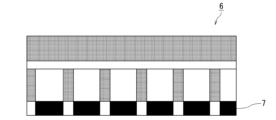
実施形態の放射線検出器は、上述した実施形態のセラミックシンチレータアレイ1を、入射した放射線に応じて光を放射する蛍光発生手段として具備し、さらに蛍光発生手段からの光を受け、光の出力を電気的出力に変換する光電変換手段を具備する。図3は実施形態の放射線検出器の一例であるX線検出器を示している。図3に示すX線線検出器6は、蛍光発生手段としてセラミックシンチレータアレイ1と、光電変換手段としてフォトダイオードのような光電変換素子7とを具備している。
(Radiation detector)
The radiation detector of the embodiment includes the
セラミックシンチレータアレイ1はX線入射面を有し、X線入射面とは反対側の面には光電変換素子7が一体的に設置されている。光電変換素子7としては、例えばフォトダイオードが使用される。光電変換素子7は、セラミックシンチレータアレイ2を構成する複数のシンチレータセグメント2のそれぞれに対応するように配置されている。これらによって、放射線検出器が構成されている。
The
セラミックシンチレータアレイ1のX線入射面には、反射層4を適宜設けることができる。反射層4は、シンチレータアレイ1から放射される可視光の反射効率がさらに向上し、ひいてはシンチレータアレイ1の光出力を高めることができる。反射層4には、反射粒子と透明樹脂との混合物やラッカー系塗料等が用いられる。反射粒子と透明樹脂との混合物は、反射層3と同様な構成を有していることが好ましい。反射層4は、反射粒子を含む透明樹脂を塗布、形成することが出来、または予め反射粒子を含む樹脂でシート状に成型されたものを、接着層5を介して、シンチレータアレイ上に張り合わせることも可能である。反射層4の厚さは50~250μmの範囲が好ましい。反射層4の厚さが50μm未満であると、反射効率の向上効果を十分に得ることができない。反射層4の厚さが250μmを超えると、透過するX線量が低下して検出感度が低下する。
A
(放射線検査装置)
実施形態の放射線検査装置は、被検査体に向けて放射線を照射する放射線源と、被検査体を透過した放射線を検出する放射線検出器とを具備する。放射線検出器には、上述した実施形態の放射線検出器が用いられる。図4は実施形態の放射線検査装置の一例であるX線CT装置10を示している。図4において、10はX線CT装置、11は被検体、12はX線管、13はコンピュータ、14はディスプレイ、15は被検体画像である。X線CT装置10は、実施形態のX線検出器6を備えている。X線検出器6は、例えば被検体11の撮像部位が配置される円筒の内壁面に貼り付けられている。X線検出器6が貼り付けられた円筒の円弧の略中心には、X線を出射するX線管12が設置されている。X線検出器6とX線管12との間には被検体11が配置される。X線検出器6のX線入射面側には、図示しないコリメータが設けられている。
(Radiation Inspection Equipment)
The radiation inspection apparatus of the embodiment includes a radiation source that irradiates radiation toward an object to be inspected, and a radiation detector that detects radiation that has passed through the object to be inspected. The radiation detector of the above-described embodiment is used as the radiation detector. FIG. 4 shows an
X線検出器6およびX線管12は、被検体11を中心にしてX線による撮影を行いながら回転するように構成されている。被検体11の画像情報が異なる角度から立体的に集められる。X線撮影により得られた信号(光電変換素子により変換された電気信号)はコンピュータ13で処理され、ディスプレイ14上に被検体画像15として表示される。被検体画像15は、例えば被検体11の断層像である。図1に示すように、シンチレータセグメント2を2次元的に配置したシンチレータアレイ1を用いることによって、マルチ断層像タイプのX線CT装置10を構成することも可能である。この場合、被検体11の断層像が複数同時に撮影され、例えば撮影結果を立体的に描写することもできる。
The
図4に示すX線CT装置10は、実施形態のセラミックシンチレータアレイ1を有するX線検出器6を具備している。前述したように、実施形態のセラミックシンチレータアレイ1は反射層3の構成等に基づいて、シンチレータセグメント2から放射される可視光の反射効率が高いため、優れた光出力を有している。このようなシンチレータアレイ1を有するX線検出器6を使用することによって、X線CT装置10による撮影時間を短くすることができる。その結果、被検体11の被爆時間を短くすることができ、低被爆化を実現することが可能になる。実施形態の放射線検査装置(X線CT装置10)は、人体の医療診断用のX線検査に限らず、動物のX線検査や工業用途のX線検査等に対しても適用可能である。さらに、X線非破壊検査装置による検査精度の向上等にも寄与する。
The
次に、本発明の具体的な実施例およびその評価結果について述べる。 Next, we will describe specific examples of the present invention and their evaluation results.
実施例及び比較例を示すにあたり、GOSセラミック板を次のように製作した。
Gd2O2S:Pr(Pr濃度=0.05モル%)の組成を有する蛍光体粉末をラバープレスにより仮成形し、この仮成形体をTa製のカプセル中に脱気密封した後、これをHIP処理装置にセットした。HIP処理装置にアルゴンガスを加圧媒体として封入し、圧力147MPa、温度1425℃の条件で3時間処理した。このようにして、直径約80mm×高さ約120mmの円柱状の焼結体を作製した。この焼結体から、種々のサイズのGOSセラミック板を切り出し、実施例および比較例に供した。
In demonstrating the examples and comparative examples, GOS ceramic plates were fabricated as follows.
A phosphor powder having a composition of Gd2O2S :Pr (Pr concentration = 0.05 mol %) was preformed by a rubber press, and the preform was degassed and sealed in a capsule made of Ta, and then set in a HIP processing device. Argon gas was sealed in the HIP processing device as a pressure medium, and the device was processed for 3 hours under the conditions of a pressure of 147 MPa and a temperature of 1425°C. In this way, a cylindrical sintered body with a diameter of about 80 mm and a height of about 120 mm was produced. GOS ceramic plates of various sizes were cut out from the sintered body and used in the examples and comparative examples.
シンチレータアレイの反りは、次のように計測した。反り返ったシンチレータアレイは、通常凸側と凹側に分かれる。反りの測定では、先ずシンチレータアレイの凸側を下に平面上に置く。このときシンチレータアレイは端部に行くにつれ、設置面から離れ、上にせり上がる状態となる。この状態で最もせり上がった点と設置面との鉛直距離を計測し、それを反りの値とした。下記実施例に記載する硬度は反射層に使用する同材料のブロックをデュロメータにて測定した。シンチレータ層において硬度を把握する場合は、デュロメータによる測定または、圧子にて反射層を押し、反射層自体が凹み、圧力を開放した際に凹みが戻る傾向であれば、デュロメータ硬度でタイプAタイプの範囲であることを推測することができる。
(実施例1)
The warpage of the scintillator array was measured as follows. A warped scintillator array is usually divided into a convex side and a concave side. In measuring the warpage, the scintillator array is first placed on a flat surface with the convex side facing down. At this time, the scintillator array moves away from the installation surface toward the end, and rises upward. In this state, the vertical distance between the most raised point and the installation surface was measured, and this was taken as the value of the warpage. The hardness described in the following examples was measured with a durometer on a block of the same material used for the reflective layer. When determining the hardness of the scintillator layer, it can be estimated that the hardness is within the range of Type A type by measuring with a durometer or by pressing the reflective layer with an indenter, and if the reflective layer itself is indented and the indentation tends to return when the pressure is released, it can be inferred that the hardness is within the range of Type A type by durometer hardness.
Example 1
長さ76mm、幅25mm、厚さ1mmのGOSセラミック板にダイシングによる溝加工を施し,溝に酸化チタンを混合したエポキシ樹脂(硬化後のガラス転移点5℃)を流し込み,熱硬化,研磨することで本発明のシンチレータアレイを作製した。反りは60μm、シンチレータセグメント間反射層のデュロメータ硬度はAタイプで50であった。
(実施例2)
A GOS ceramic plate 76 mm long, 25 mm wide, and 1 mm thick was diced to create grooves, and epoxy resin (glass transition point after curing: 5°C) mixed with titanium oxide was poured into the grooves, followed by thermal curing and polishing to produce a scintillator array of the present invention. The warpage was 60 μm, and the durometer hardness of the reflective layer between the scintillator segments was 50 for type A.
Example 2
長さ76mm、幅25mm、厚さ1mmのGOSセラミック板にダイシングによる溝加工を施し,溝に酸化チタンを混合したエポキシ樹脂(硬化後のガラス転移点10℃)を流し込み,熱硬化,研磨することで本発明のシンチレータアレイを作製した。反りは75μm、シンチレータセグメント間反射層のデュロメータ硬度はAタイプで70であった。
(実施例3)
A GOS ceramic plate 76 mm long, 25 mm wide, and 1 mm thick was diced to create grooves, and epoxy resin (glass transition point after curing: 10°C) mixed with titanium oxide was poured into the grooves, followed by thermal curing and polishing to produce a scintillator array of the present invention. The warpage was 75 μm, and the durometer hardness of the reflective layer between the scintillator segments was 70 for type A.
Example 3
長さ76mm、幅25mm、厚さ1mmのGOSセラミック板にダイシングによる溝加工を施し,溝に酸化チタンを混合したエポキシ樹脂(硬化後のガラス転移点5℃)を流し込み,熱硬化,研磨することでシンチレータを形成した。このシンチレータのX線入射面に酸化チタンを含有したエポキシ樹脂(硬化後のガラス転移点5℃)を塗布し,100℃,3時間で硬化させた。厚みを150μmにするため、硬化後に研磨し,反射層を形成した。反りは80μm、シンチレータセグメント間反射層のデュロメータ硬度はAタイプで50であった。
(実施例4)
A GOS ceramic plate with a length of 76 mm, width of 25 mm, and thickness of 1 mm was diced to create grooves, and epoxy resin (glass transition point after curing: 5°C) mixed with titanium oxide was poured into the grooves, followed by heat curing and polishing to form a scintillator. An epoxy resin (glass transition point after curing: 5°C) containing titanium oxide was applied to the X-ray incidence surface of this scintillator and cured at 100°C for 3 hours. To make the thickness 150 μm, the plate was polished after curing to form a reflective layer. The warp was 80 μm, and the durometer hardness of the reflective layer between the scintillator segments was 50 for type A.
Example 4
長さ76mm、幅25mm、厚さ1mmのGOSセラミック板にダイシングによる溝加工を施し,溝に酸化チタンを混合したエポキシ樹脂(硬化後のガラス転移点5℃)を流し込み,熱硬化,研磨することでシンチレータを形成した.このシンチレータ上に白色PETフィルム(三菱ケミカル製,厚み100μm)をプリプレグ状態のエポキシ接着シート厚み(25μm)を用いて貼り合わせた。張り合わせる際にはシンチレータ,エポキシ接着シート,白色PETシートを重ねて,荷重16kg印加し,100℃で加熱して接着した。常温まで冷却後に荷重を除き完成させた。反りは80μmであり、シンチレータセグメント間反射層のデュロメータ硬度はAタイプで50であった。
(実施例5)
A GOS ceramic plate with a length of 76 mm, width of 25 mm, and thickness of 1 mm was diced to create grooves, and epoxy resin (glass transition point after curing: 5°C) mixed with titanium oxide was poured into the grooves, followed by heat curing and polishing to form a scintillator. A white PET film (manufactured by Mitsubishi Chemical, thickness 100 μm) was attached onto the scintillator using a prepreg-state epoxy adhesive sheet (thickness 25 μm). When attaching, the scintillator, epoxy adhesive sheet, and white PET sheet were stacked, and a load of 16 kg was applied, and they were heated to 100°C to bond them. After cooling to room temperature, the load was removed to complete the assembly. The warp was 80 μm, and the durometer hardness of the reflective layer between the scintillator segments was 50 for type A.
Example 5
長さ76mm、幅25mm、厚さ1mmのGOSセラミック板にダイシングによる溝加工を施し,溝に酸化チタンを混合したエポキシ樹脂(硬化後のガラス転移点15℃)を流し込み,熱硬化,研磨することでシンチレータを形成した。このシンチレータ上に酸化チタンを含有したエポキシ接着剤を厚み10μmで塗布し、その上に白色PETフィルム(厚み100μm)を設置し、荷重をかけながら常温で24時間硬化させた。荷重を除去後,反りを測定した結果,100μmであり、シンチレータセグメント間反射層のデュロメータ硬度はAタイプで95であった。
(比較例1)
A GOS ceramic plate with a length of 76 mm, width of 25 mm, and thickness of 1 mm was diced to create grooves, and epoxy resin (glass transition point after curing: 15°C) mixed with titanium oxide was poured into the grooves, followed by heat curing and polishing to form a scintillator. An epoxy adhesive containing titanium oxide was applied to a thickness of 10 μm on this scintillator, and a white PET film (thickness of 100 μm) was placed on top of it, and cured at room temperature for 24 hours while applying a load. After removing the load, the warp was measured to be 100 μm, and the durometer hardness of the reflective layer between the scintillator segments was 95 for type A.
Comparative Example 1
長さ76mm、幅25mm、厚さ1mmのGOSセラミック板にダイシングによる溝加工を施し,溝に酸化チタンを混合したエポキシ樹脂(硬化後のガラス転移点85℃)を流し込み,熱硬化,研磨することで本発明のシンチレータアレイを作製した。反りを測定した結果、反りは55μmであった。またシンチレータセグメント間反射層のデュロメータ硬度はDタイプで85であった。
(比較例2)
A GOS ceramic plate 76 mm long, 25 mm wide, and 1 mm thick was diced to create grooves, and epoxy resin (glass transition point after curing: 85°C) mixed with titanium oxide was poured into the grooves, followed by thermal curing and polishing to produce a scintillator array of the present invention. The warpage was measured to be 55 μm. The durometer hardness of the reflective layer between the scintillator segments was 85 for D type.
(Comparative Example 2)
長さ76mm、幅25mm、厚さ1mmのGOSセラミック板にダイシングによる溝加工を施し,溝に酸化チタンを混合したエポキシ樹脂(硬化後のガラス転移点90℃)を流し込み,熱硬化,研磨することで本発明のシンチレータアレイを作製した。反りを測定した結果、反りは40μmであった。またシンチレータセグメント間反射層のデュロメータ硬度はDタイプで80であった。
(比較例3)
A GOS ceramic plate with a length of 76 mm, a width of 25 mm, and a thickness of 1 mm was diced to create grooves, and an epoxy resin (glass transition point after curing: 90°C) mixed with titanium oxide was poured into the grooves, followed by thermal curing and polishing to produce a scintillator array of the present invention. The warpage was measured to be 40 μm. The durometer hardness of the reflective layer between the scintillator segments was 80 for D type.
(Comparative Example 3)
長さ76mm、幅25mm、厚さ1mmのGOSセラミック板にダイシングによる溝加工を施し,溝に酸化チタンを混合したエポキシ樹脂(硬化後のガラス転移点75℃)を流し込み,熱硬化,研磨することでシンチレータを形成した.このシンチレータ上に白色PETフィルム(三菱ケミカル製,厚み100μm)をプリプレグ状態のエポキシ接着シート厚み(25μm)を用いて貼り合わせた。張り合わせる際にはシンチレータ,エポキシ接着シート,白色PETシートを重ねて,荷重16kg印加し,100℃で加熱して接着した。常温まで冷却後に荷重を除き完成させた。反りを測定した結果、反りは45μmであった。またシンチレータセグメント間反射層のデュロメータ硬度はDタイプで75であった。
次にフォトダイオード上に接着剤を塗布し,実施例1~5及び比較例1~3によって得られたシンチレータアレイを貼り合わせ、接着層の厚みを測定した結果を表2に示した。貼り合わせる際にシンチレータに荷重をかけることで反りを矯正しつつ貼り付けた。
A GOS ceramic plate with a length of 76 mm, width of 25 mm, and thickness of 1 mm was diced to create grooves, and epoxy resin (glass transition point after curing: 75°C) mixed with titanium oxide was poured into the grooves, and the scintillator was formed by heat curing and polishing. A white PET film (manufactured by Mitsubishi Chemical, thickness 100 μm) was attached to the scintillator using a prepreg-state epoxy adhesive sheet (thickness 25 μm). When attaching, the scintillator, epoxy adhesive sheet, and white PET sheet were stacked, and a load of 16 kg was applied, and they were heated to 100°C to bond them. After cooling to room temperature, the load was removed and the product was completed. The warp was measured and found to be 45 μm. The durometer hardness of the reflective layer between the scintillator segments was 75 for D type.
Next, an adhesive was applied onto the photodiode, and the scintillator arrays obtained in Examples 1 to 5 and Comparative Examples 1 to 3 were attached thereto, and the thickness of the adhesive layer was measured, and the results are shown in Table 2. When attaching the scintillators, a load was applied to the scintillators to correct any warping while attaching them.
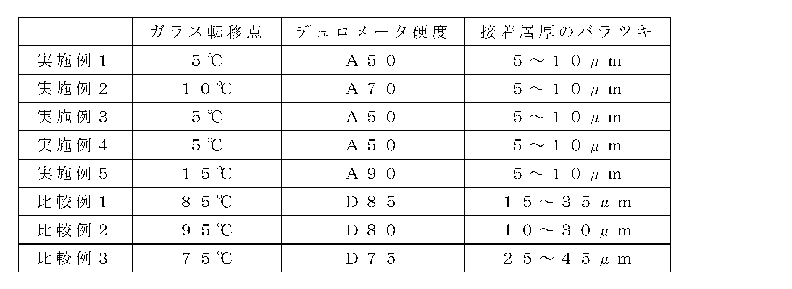
表2から、従来より用いられてきた透明樹脂のガラス転移点が、放射線検査装置の使用温度(50~60℃)より高いものでは、シンチレータアレイそのものの反りは小さいものの、フォトダイオードアレイに張り合わせたときの、接着層厚のバラツキ幅は、20μmと比較的大きい値を示した。一方、本発明のシンチレータアレイの場合には、その反りは大きかったものの、張り合わせた時の、接着層は均一にフォトダイオードアレイ密着するせいか、接着層厚のバラツキ幅は、5μmと小さい結果が得られた。こうした結果と相関するように、本発明のシンチレータアレイの反射層のデュロメータ硬度は、従来の反射層のデュロメータ硬度よりも明らかに小さい値であった。 As can be seen from Table 2, when the glass transition point of the conventionally used transparent resin is higher than the operating temperature of the radiation inspection device (50-60°C), the warping of the scintillator array itself is small, but the variation in the adhesive layer thickness when bonded to the photodiode array is relatively large at 20 μm. On the other hand, in the case of the scintillator array of the present invention, although the warping is large, the variation in the adhesive layer thickness is small at 5 μm, probably because the adhesive layer adheres uniformly to the photodiode array when bonded. Correlating with these results, the durometer hardness of the reflective layer of the scintillator array of the present invention is clearly smaller than the durometer hardness of the conventional reflective layer.
本発明のシンチレータアレイによれば、検出器であるフォトダイオードアレイに密着させられることにより、接着層が均一となる。これはシンチレータセグメント間の漏光を少なくすることができ、画像情報のクロストークを低減できるため、産業上有用なものと言える。 The scintillator array of the present invention is attached to the photodiode array, which is the detector, so that the adhesive layer is uniform. This can reduce light leakage between the scintillator segments and reduce crosstalk in image information, making it industrially useful.
1 シンチレータアレイ
2 シンチレータセグメント
3 シンチレータセグメント間の反射層
4 X線入射面側のシンチレータアレイに付設される反射層
5 接着層
6 X線検出器
7 光電変換素子
Claims (10)
前記複数のシンチレータセグメントのうち隣り合うシンチレータセグメントの間に設けられ、ガラス転移点が0℃以上40℃以下である第一の反射層と、
を有する、セラミックスシンチレータアレイ。 A plurality of scintillator segments;
a first reflective layer provided between adjacent ones of the plurality of scintillator segments and having a glass transition point of 0 ° C. or more and 40 ° C. or less;
A ceramic scintillator array comprising:
一般式:RE2O2S:Pr
(ここで、REはY、Gd、La、およびLuからなる群より選ばれる少なくとも1つである)で表され、RE2O2Sに対するPrの含有量が0.001モル%以上10モル%以下である組成を有することを特徴とするセラミックスシンチレータアレイ。 In the ceramic scintillator array according to any one of claims 1 to 5, the rare earth oxysulfide phosphor is
General formula: RE 2 O 2 S: Pr
(wherein RE is at least one selected from the group consisting of Y, Gd, La, and Lu), and the content of Pr relative to RE 2 O 2 S is 0.001 mol % or more and 10 mol % or less.
Priority Applications (2)
| Application Number | Priority Date | Filing Date | Title |
|---|---|---|---|
| JP2023153674A JP7516640B2 (en) | 2019-11-05 | 2023-09-20 | Ceramic scintillator array, and radiation detector and radiation inspection device using the same |
| JP2024103801A JP2024120091A (en) | 2019-11-05 | 2024-06-27 | Ceramic scintillator array, and radiation detector and radiation inspection device using the same |
Applications Claiming Priority (2)
| Application Number | Priority Date | Filing Date | Title |
|---|---|---|---|
| JP2019200890A JP7355608B2 (en) | 2019-11-05 | 2019-11-05 | Ceramic scintillator array, radiation detector and radiation inspection equipment using it |
| JP2023153674A JP7516640B2 (en) | 2019-11-05 | 2023-09-20 | Ceramic scintillator array, and radiation detector and radiation inspection device using the same |
Related Parent Applications (1)
| Application Number | Title | Priority Date | Filing Date |
|---|---|---|---|
| JP2019200890A Division JP7355608B2 (en) | 2019-11-05 | 2019-11-05 | Ceramic scintillator array, radiation detector and radiation inspection equipment using it |
Related Child Applications (1)
| Application Number | Title | Priority Date | Filing Date |
|---|---|---|---|
| JP2024103801A Division JP2024120091A (en) | 2019-11-05 | 2024-06-27 | Ceramic scintillator array, and radiation detector and radiation inspection device using the same |
Publications (2)
| Publication Number | Publication Date |
|---|---|
| JP2023168392A JP2023168392A (en) | 2023-11-24 |
| JP7516640B2 true JP7516640B2 (en) | 2024-07-16 |
Family
ID=75897794
Family Applications (3)
| Application Number | Title | Priority Date | Filing Date |
|---|---|---|---|
| JP2019200890A Active JP7355608B2 (en) | 2019-11-05 | 2019-11-05 | Ceramic scintillator array, radiation detector and radiation inspection equipment using it |
| JP2023153674A Active JP7516640B2 (en) | 2019-11-05 | 2023-09-20 | Ceramic scintillator array, and radiation detector and radiation inspection device using the same |
| JP2024103801A Pending JP2024120091A (en) | 2019-11-05 | 2024-06-27 | Ceramic scintillator array, and radiation detector and radiation inspection device using the same |
Family Applications Before (1)
| Application Number | Title | Priority Date | Filing Date |
|---|---|---|---|
| JP2019200890A Active JP7355608B2 (en) | 2019-11-05 | 2019-11-05 | Ceramic scintillator array, radiation detector and radiation inspection equipment using it |
Family Applications After (1)
| Application Number | Title | Priority Date | Filing Date |
|---|---|---|---|
| JP2024103801A Pending JP2024120091A (en) | 2019-11-05 | 2024-06-27 | Ceramic scintillator array, and radiation detector and radiation inspection device using the same |
Country Status (1)
| Country | Link |
|---|---|
| JP (3) | JP7355608B2 (en) |
Families Citing this family (2)
| Publication number | Priority date | Publication date | Assignee | Title |
|---|---|---|---|---|
| WO2025069781A1 (en) | 2023-09-28 | 2025-04-03 | Agc株式会社 | Sulfide solid electrolyte and method for manufacturing same |
| CN117777890B (en) * | 2023-11-29 | 2024-11-05 | 奕瑞新材料科技(太仓)有限公司 | Anti-crosstalk reflective filler, anti-crosstalk pouring sealant and medical CT scintillator ceramic area array |
Citations (1)
| Publication number | Priority date | Publication date | Assignee | Title |
|---|---|---|---|---|
| WO2017110850A1 (en) | 2015-12-25 | 2017-06-29 | 株式会社 東芝 | Ceramic scintillator array, x-ray detector, and x-ray inspection device |
Family Cites Families (2)
| Publication number | Priority date | Publication date | Assignee | Title |
|---|---|---|---|---|
| EP2220516B1 (en) * | 2007-11-06 | 2018-05-02 | Koninklijke Philips N.V. | Radiation detector comprising a light reflective material |
| EP3499272A1 (en) * | 2017-12-14 | 2019-06-19 | Koninklijke Philips N.V. | Structured surface part for radiation capturing devices, method of manufacturing such a part and x-ray detector |
-
2019
- 2019-11-05 JP JP2019200890A patent/JP7355608B2/en active Active
-
2023
- 2023-09-20 JP JP2023153674A patent/JP7516640B2/en active Active
-
2024
- 2024-06-27 JP JP2024103801A patent/JP2024120091A/en active Pending
Patent Citations (1)
| Publication number | Priority date | Publication date | Assignee | Title |
|---|---|---|---|---|
| WO2017110850A1 (en) | 2015-12-25 | 2017-06-29 | 株式会社 東芝 | Ceramic scintillator array, x-ray detector, and x-ray inspection device |
Also Published As
| Publication number | Publication date |
|---|---|
| JP2023168392A (en) | 2023-11-24 |
| JP2021076394A (en) | 2021-05-20 |
| JP7355608B2 (en) | 2023-10-03 |
| JP2024120091A (en) | 2024-09-03 |
Similar Documents
| Publication | Publication Date | Title |
|---|---|---|
| US10416319B2 (en) | Ceramic scintillator array, method for manufacturing same, radiation detector and radiation inspection device | |
| US10281591B2 (en) | Ceramic scintillator array, X-ray detector, and X-ray inspection device | |
| JP7516640B2 (en) | Ceramic scintillator array, and radiation detector and radiation inspection device using the same | |
| US12517269B2 (en) | Scintillator array, and radiation detector and radiation inspection apparatus using the same | |
| JP7662865B2 (en) | Scintillator array, radiation detector, and radiation inspection device | |
| JP7717766B6 (en) | Scintillator array, radiation detector, and radiation inspection device | |
| WO2024203657A1 (en) | Scintillator array, x-ray detector, and x-ray inspection device |
Legal Events
| Date | Code | Title | Description |
|---|---|---|---|
| A621 | Written request for application examination |
Free format text: JAPANESE INTERMEDIATE CODE: A621 Effective date: 20230920 |
|
| A977 | Report on retrieval |
Free format text: JAPANESE INTERMEDIATE CODE: A971007 Effective date: 20240322 |
|
| A131 | Notification of reasons for refusal |
Free format text: JAPANESE INTERMEDIATE CODE: A131 Effective date: 20240402 |
|
| A521 | Request for written amendment filed |
Free format text: JAPANESE INTERMEDIATE CODE: A523 Effective date: 20240527 |
|
| TRDD | Decision of grant or rejection written | ||
| A01 | Written decision to grant a patent or to grant a registration (utility model) |
Free format text: JAPANESE INTERMEDIATE CODE: A01 Effective date: 20240604 |
|
| A61 | First payment of annual fees (during grant procedure) |
Free format text: JAPANESE INTERMEDIATE CODE: A61 Effective date: 20240703 |
|
| R150 | Certificate of patent or registration of utility model |
Ref document number: 7516640 Country of ref document: JP Free format text: JAPANESE INTERMEDIATE CODE: R150 |
|
| S111 | Request for change of ownership or part of ownership |
Free format text: JAPANESE INTERMEDIATE CODE: R313117 |
|
| S533 | Written request for registration of change of name |
Free format text: JAPANESE INTERMEDIATE CODE: R313533 |
|
| R350 | Written notification of registration of transfer |
Free format text: JAPANESE INTERMEDIATE CODE: R350 |
|
| R350 | Written notification of registration of transfer |
Free format text: JAPANESE INTERMEDIATE CODE: R350 |