EP3385986B1 - Display panel and display device having the same - Google Patents
Display panel and display device having the same Download PDFInfo
- Publication number
- EP3385986B1 EP3385986B1 EP18154285.3A EP18154285A EP3385986B1 EP 3385986 B1 EP3385986 B1 EP 3385986B1 EP 18154285 A EP18154285 A EP 18154285A EP 3385986 B1 EP3385986 B1 EP 3385986B1
- Authority
- EP
- European Patent Office
- Prior art keywords
- electrode
- layer
- insulating layer
- display panel
- cross
- Prior art date
- Legal status (The legal status is an assumption and is not a legal conclusion. Google has not performed a legal analysis and makes no representation as to the accuracy of the status listed.)
- Active
Links
Images


Classifications
-
- G—PHYSICS
- G02—OPTICS
- G02F—OPTICAL DEVICES OR ARRANGEMENTS FOR THE CONTROL OF LIGHT BY MODIFICATION OF THE OPTICAL PROPERTIES OF THE MEDIA OF THE ELEMENTS INVOLVED THEREIN; NON-LINEAR OPTICS; FREQUENCY-CHANGING OF LIGHT; OPTICAL LOGIC ELEMENTS; OPTICAL ANALOGUE/DIGITAL CONVERTERS
- G02F1/00—Devices or arrangements for the control of the intensity, colour, phase, polarisation or direction of light arriving from an independent light source, e.g. switching, gating or modulating; Non-linear optics
- G02F1/01—Devices or arrangements for the control of the intensity, colour, phase, polarisation or direction of light arriving from an independent light source, e.g. switching, gating or modulating; Non-linear optics for the control of the intensity, phase, polarisation or colour
- G02F1/13—Devices or arrangements for the control of the intensity, colour, phase, polarisation or direction of light arriving from an independent light source, e.g. switching, gating or modulating; Non-linear optics for the control of the intensity, phase, polarisation or colour based on liquid crystals, e.g. single liquid crystal display cells
- G02F1/133—Constructional arrangements; Operation of liquid crystal cells; Circuit arrangements
- G02F1/1333—Constructional arrangements; Manufacturing methods
- G02F1/1343—Electrodes
-
- H—ELECTRICITY
- H10—SEMICONDUCTOR DEVICES; ELECTRIC SOLID-STATE DEVICES NOT OTHERWISE PROVIDED FOR
- H10D—INORGANIC ELECTRIC SEMICONDUCTOR DEVICES
- H10D86/00—Integrated devices formed in or on insulating or conducting substrates, e.g. formed in silicon-on-insulator [SOI] substrates or on stainless steel or glass substrates
- H10D86/40—Integrated devices formed in or on insulating or conducting substrates, e.g. formed in silicon-on-insulator [SOI] substrates or on stainless steel or glass substrates characterised by multiple TFTs
- H10D86/441—Interconnections, e.g. scanning lines
-
- G—PHYSICS
- G02—OPTICS
- G02F—OPTICAL DEVICES OR ARRANGEMENTS FOR THE CONTROL OF LIGHT BY MODIFICATION OF THE OPTICAL PROPERTIES OF THE MEDIA OF THE ELEMENTS INVOLVED THEREIN; NON-LINEAR OPTICS; FREQUENCY-CHANGING OF LIGHT; OPTICAL LOGIC ELEMENTS; OPTICAL ANALOGUE/DIGITAL CONVERTERS
- G02F1/00—Devices or arrangements for the control of the intensity, colour, phase, polarisation or direction of light arriving from an independent light source, e.g. switching, gating or modulating; Non-linear optics
- G02F1/01—Devices or arrangements for the control of the intensity, colour, phase, polarisation or direction of light arriving from an independent light source, e.g. switching, gating or modulating; Non-linear optics for the control of the intensity, phase, polarisation or colour
- G02F1/13—Devices or arrangements for the control of the intensity, colour, phase, polarisation or direction of light arriving from an independent light source, e.g. switching, gating or modulating; Non-linear optics for the control of the intensity, phase, polarisation or colour based on liquid crystals, e.g. single liquid crystal display cells
- G02F1/133—Constructional arrangements; Operation of liquid crystal cells; Circuit arrangements
- G02F1/136—Liquid crystal cells structurally associated with a semi-conducting layer or substrate, e.g. cells forming part of an integrated circuit
- G02F1/1362—Active matrix addressed cells
- G02F1/136227—Through-hole connection of the pixel electrode to the active element through an insulation layer
-
- G—PHYSICS
- G02—OPTICS
- G02F—OPTICAL DEVICES OR ARRANGEMENTS FOR THE CONTROL OF LIGHT BY MODIFICATION OF THE OPTICAL PROPERTIES OF THE MEDIA OF THE ELEMENTS INVOLVED THEREIN; NON-LINEAR OPTICS; FREQUENCY-CHANGING OF LIGHT; OPTICAL LOGIC ELEMENTS; OPTICAL ANALOGUE/DIGITAL CONVERTERS
- G02F1/00—Devices or arrangements for the control of the intensity, colour, phase, polarisation or direction of light arriving from an independent light source, e.g. switching, gating or modulating; Non-linear optics
- G02F1/01—Devices or arrangements for the control of the intensity, colour, phase, polarisation or direction of light arriving from an independent light source, e.g. switching, gating or modulating; Non-linear optics for the control of the intensity, phase, polarisation or colour
- G02F1/13—Devices or arrangements for the control of the intensity, colour, phase, polarisation or direction of light arriving from an independent light source, e.g. switching, gating or modulating; Non-linear optics for the control of the intensity, phase, polarisation or colour based on liquid crystals, e.g. single liquid crystal display cells
- G02F1/133—Constructional arrangements; Operation of liquid crystal cells; Circuit arrangements
- G02F1/136—Liquid crystal cells structurally associated with a semi-conducting layer or substrate, e.g. cells forming part of an integrated circuit
- G02F1/1362—Active matrix addressed cells
- G02F1/136286—Wiring, e.g. gate line, drain line
- G02F1/136295—Materials; Compositions; Manufacture processes
-
- H—ELECTRICITY
- H10—SEMICONDUCTOR DEVICES; ELECTRIC SOLID-STATE DEVICES NOT OTHERWISE PROVIDED FOR
- H10D—INORGANIC ELECTRIC SEMICONDUCTOR DEVICES
- H10D30/00—Field-effect transistors [FET]
- H10D30/60—Insulated-gate field-effect transistors [IGFET]
- H10D30/67—Thin-film transistors [TFT]
- H10D30/6729—Thin-film transistors [TFT] characterised by the electrodes
- H10D30/6737—Thin-film transistors [TFT] characterised by the electrodes characterised by the electrode materials
-
- H—ELECTRICITY
- H10—SEMICONDUCTOR DEVICES; ELECTRIC SOLID-STATE DEVICES NOT OTHERWISE PROVIDED FOR
- H10D—INORGANIC ELECTRIC SEMICONDUCTOR DEVICES
- H10D86/00—Integrated devices formed in or on insulating or conducting substrates, e.g. formed in silicon-on-insulator [SOI] substrates or on stainless steel or glass substrates
- H10D86/40—Integrated devices formed in or on insulating or conducting substrates, e.g. formed in silicon-on-insulator [SOI] substrates or on stainless steel or glass substrates characterised by multiple TFTs
- H10D86/451—Integrated devices formed in or on insulating or conducting substrates, e.g. formed in silicon-on-insulator [SOI] substrates or on stainless steel or glass substrates characterised by multiple TFTs characterised by the compositions or shapes of the interlayer dielectrics
-
- H—ELECTRICITY
- H10—SEMICONDUCTOR DEVICES; ELECTRIC SOLID-STATE DEVICES NOT OTHERWISE PROVIDED FOR
- H10D—INORGANIC ELECTRIC SEMICONDUCTOR DEVICES
- H10D86/00—Integrated devices formed in or on insulating or conducting substrates, e.g. formed in silicon-on-insulator [SOI] substrates or on stainless steel or glass substrates
- H10D86/40—Integrated devices formed in or on insulating or conducting substrates, e.g. formed in silicon-on-insulator [SOI] substrates or on stainless steel or glass substrates characterised by multiple TFTs
- H10D86/60—Integrated devices formed in or on insulating or conducting substrates, e.g. formed in silicon-on-insulator [SOI] substrates or on stainless steel or glass substrates characterised by multiple TFTs wherein the TFTs are in active matrices
-
- H—ELECTRICITY
- H10—SEMICONDUCTOR DEVICES; ELECTRIC SOLID-STATE DEVICES NOT OTHERWISE PROVIDED FOR
- H10K—ORGANIC ELECTRIC SOLID-STATE DEVICES
- H10K59/00—Integrated devices, or assemblies of multiple devices, comprising at least one organic light-emitting element covered by group H10K50/00
- H10K59/10—OLED displays
- H10K59/12—Active-matrix OLED [AMOLED] displays
- H10K59/131—Interconnections, e.g. wiring lines or terminals
-
- G—PHYSICS
- G02—OPTICS
- G02F—OPTICAL DEVICES OR ARRANGEMENTS FOR THE CONTROL OF LIGHT BY MODIFICATION OF THE OPTICAL PROPERTIES OF THE MEDIA OF THE ELEMENTS INVOLVED THEREIN; NON-LINEAR OPTICS; FREQUENCY-CHANGING OF LIGHT; OPTICAL LOGIC ELEMENTS; OPTICAL ANALOGUE/DIGITAL CONVERTERS
- G02F1/00—Devices or arrangements for the control of the intensity, colour, phase, polarisation or direction of light arriving from an independent light source, e.g. switching, gating or modulating; Non-linear optics
- G02F1/01—Devices or arrangements for the control of the intensity, colour, phase, polarisation or direction of light arriving from an independent light source, e.g. switching, gating or modulating; Non-linear optics for the control of the intensity, phase, polarisation or colour
- G02F1/13—Devices or arrangements for the control of the intensity, colour, phase, polarisation or direction of light arriving from an independent light source, e.g. switching, gating or modulating; Non-linear optics for the control of the intensity, phase, polarisation or colour based on liquid crystals, e.g. single liquid crystal display cells
- G02F1/133—Constructional arrangements; Operation of liquid crystal cells; Circuit arrangements
- G02F1/1333—Constructional arrangements; Manufacturing methods
- G02F1/133345—Insulating layers
-
- G—PHYSICS
- G02—OPTICS
- G02F—OPTICAL DEVICES OR ARRANGEMENTS FOR THE CONTROL OF LIGHT BY MODIFICATION OF THE OPTICAL PROPERTIES OF THE MEDIA OF THE ELEMENTS INVOLVED THEREIN; NON-LINEAR OPTICS; FREQUENCY-CHANGING OF LIGHT; OPTICAL LOGIC ELEMENTS; OPTICAL ANALOGUE/DIGITAL CONVERTERS
- G02F1/00—Devices or arrangements for the control of the intensity, colour, phase, polarisation or direction of light arriving from an independent light source, e.g. switching, gating or modulating; Non-linear optics
- G02F1/01—Devices or arrangements for the control of the intensity, colour, phase, polarisation or direction of light arriving from an independent light source, e.g. switching, gating or modulating; Non-linear optics for the control of the intensity, phase, polarisation or colour
- G02F1/13—Devices or arrangements for the control of the intensity, colour, phase, polarisation or direction of light arriving from an independent light source, e.g. switching, gating or modulating; Non-linear optics for the control of the intensity, phase, polarisation or colour based on liquid crystals, e.g. single liquid crystal display cells
- G02F1/133—Constructional arrangements; Operation of liquid crystal cells; Circuit arrangements
- G02F1/136—Liquid crystal cells structurally associated with a semi-conducting layer or substrate, e.g. cells forming part of an integrated circuit
- G02F1/1362—Active matrix addressed cells
- G02F1/1368—Active matrix addressed cells in which the switching element is a three-electrode device
-
- G—PHYSICS
- G09—EDUCATION; CRYPTOGRAPHY; DISPLAY; ADVERTISING; SEALS
- G09G—ARRANGEMENTS OR CIRCUITS FOR CONTROL OF INDICATING DEVICES USING STATIC MEANS TO PRESENT VARIABLE INFORMATION
- G09G2310/00—Command of the display device
- G09G2310/02—Addressing, scanning or driving the display screen or processing steps related thereto
- G09G2310/0264—Details of driving circuits
Definitions
- the present disclosure relates to a display panel and a display device having the same.
- a display device is a device that includes a display panel.
- Display panels generally include a plurality of pixels.
- Display panels may be of various types such as a liquid-crystal display device (LCD device) and an organic light-emitting diode display (OLED display device), etc.
- a liquid-crystal display panel which is used in a liquid-crystal display device, is composed of two substrates on which electric field generating electrodes, such as pixel electrodes and common electrodes, are formed. A liquid-crystal layer is injected between the two substrates. Voltage is applied to the electric field generating electrodes to form an electric field across the liquid-crystal layer. As a result of the electric field, the orientation of the liquid crystals contained in the liquid-crystal layer is aligned and the polarization of incident light is controlled, thereby displaying an image.
- electric field generating electrodes such as pixel electrodes and common electrodes
- the pixel electrode is connected to a switching device such as a thin-film transistor (TFT) and receives a data voltage corresponding to a video signal input to the display panel.
- a switching device such as a thin-film transistor (TFT) and receives a data voltage corresponding to a video signal input to the display panel.
- TFT thin-film transistor
- US2011084268 discloses a semiconductor device where a wiring with low resistance is connected to a thin film transistor in which a source electrode and a drain electrode connected to an oxide semiconductor layer with a suppressed impurity concentration.
- the thin film transistor including the oxide semiconductor may be surrounded by insulating films to be sealed.
- an electronic apparatus may be any apparatus that includes a display device.
- the electronic apparatus may include smart phones, mobile phones, wearable devices such as smart watches, turn-by-turn navigation systems, video game consoles, TVs, car head units, notebook computers, laptop computers, tablet computers, personal media players (PMPs), and personal digital assistants (PDAs).
- the electronic apparatus may be embodied as a pocket-sized portable communication terminal having a wireless communication function.
- the display device may be a flexible display device capable of being bent into an orientation other than flat.
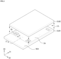
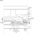
- FIG. 1 is a perspective view illustrating a display panel according to an exemplary embodiment of the present disclosure.
- a display panel includes a first display substrate SUB1 and a second display substrate SUB2.
- the second display substrate SUB2 has a smaller area than the first display substrate SUB1.
- the second display substrate SUB2 overlaps with the first display substrate SUB1.
- Liquid crystals LC are injected into a space between the first display substrate SUB1 and the second display substrate SUB2 to form a liquid-crystal layer LCL between the first display substrate SUB1 and the second display substrate SB2.
- a surface of the first display substrate SUB1 that faces the second display substrate SUB2 may be divided into a display area DA and a non-display area NDA.
- the display area DA may be defined as an area where a plurality of pixels PXs for displaying an image is disposed. Accordingly, an image to be displayed may be displayed entirely within the display area DA.
- the non-display area NDA may be defined as the area of the first display substrate SUB1 that is not the display area DA.
- the display area DA may be disposed entirely within an area where the first display substrate SUB1 and the second display substrate SUB2 overlap.
- the second display substrate SUB2 may fully correspond to the display area DA of the first substrate SUB1 or the second display substrate SUB2 may cover a portion of the non-display area NDA as well as an entirety of the display area DA.
- the plurality of pixels PXs may be arranged in a matrix pattern along the first direction D1 and the second direction D2, which may be substantially perpendicular to each other.
- the pixels PXs may include first to third pixel types representing red color, green color and blue color pixels, respectively.
- the pixels PXs may include yellow color, cyan color, and a magenta color pixels, respectively.
- the pixels PXs may include white pixels for displaying white as well.
- the gray scale of each pixel PX may be individually controlled. Each of the pixels PX may work as a unit for displaying a particular color. The grayscale of each of the pixels PXs can be controlled by adjusting the amount of incident light that travels from below the first display substrate SUB1 toward the second display substrate SUB2.
- Various components for driving the pixels PXs such as a drive IC may be mounted in the non-display area NDA.
- Display devices include liquid-crystal display devices, organic light-emitting display device, etc. and each type of display device may have a unique structure of the pixels PXs.
- the display device is a liquid-crystal display device.
- the technical idea of exemplary embodiments of the present disclosure may equally applied to organic light-emitting display device as well.
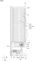
- each of the pixels PXs will be described in detail with reference to FIGS. 2 and 3 .
- FIG. 2 is a layout diagram illustrating a single pixel disposed in a display panel according to an exemplary embodiment of the present disclosure.
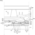
- FIG. 3 is a cross-sectional view taken along line I - I' of FIG. 2 .
- one pixel PX of the display panel includes a first display substrate SUB1, a second display substrate SUB2, and a liquid-crystal layer LCL.
- Each of the pixels PXs includes an active area ACA through which light is transmitted.
- Various components for changing the orientation of the liquid crystals LC in the liquid-crystal layer LCL such as a pixel electrode 220 and a thin-film transistor 153 may be disposed on the first display substrate SUB1.
- the second display substrate SUB2 faces the first display substrate SUB1.
- a common electrode 320 is disposed on a second base substrate 310 so as to face the pixel electrode 220.
- the liquid-crystal layer LCL is interposed between the first display substrate SUB1 and the second display substrate SUB2 and may include liquid crystals LC having dielectric anisotropy.
- the liquid crystals LC may be rotated in a particular direction between the first display substrate SUB1 and the second display substrate SUB2 to thereby change the polarization of light passing therethrough.
- rotation may refer not only to actual rotation of the liquid crystals LC but also to any change in orientation of the liquid crystals LC caused by the electric field.
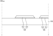
- the first display substrate SUB1 includes a first base substrate 110.
- the first base substrate 110 may be a transparent insulation substrate.
- the first base substrate 110 may be a glass substrate, a quartz substrate, a transparent resin substrate, etc.
- the first base substrate 110 may be curved in a particular direction.
- the first base substrate 110 may be flexible.
- the first base substrate 110 may be deformable so that it may be rolled, folded, bent and so on.
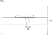
- a gate line 122, a gate electrode 124 and a sustain line 125 are each disposed on the first base substrate 110.
- the gate line 122 transfers a gate voltage for controlling the thin-film transistor 153.
- the gate line 122 may be extended in a first direction D1.
- the gate voltage is applied from an external source and may have a varying voltage level.
- the thin-film transistor 153 may be turned on and/or off in response to the voltage value of the gate signal.
- the gate electrode 124 may protrude from the gate line 122 and may be mechanically and electrically connected to the gate line 122.
- the gate electrode 124 is one of the elements of the thin-film transistor 153 which is described in greater detail below.
- the sustain line 125 is disposed such that it does not overlap with the gate line 122, and the sustain line 125 extends primarily in the first direction D1 along the edge of the active area ACA.
- the sustain line 125 may be disposed adjacent to a part of the pixel electrode 220, as is described in greater detail below.
- a capacitance may be formed between the pixel electrode 220 and the sustain line 125.
- the sustain line 125 may overlap with a part of a connection electrode 182, as is described in greater detail below.
- a capacitance may be formed between the connection electrode 182 and the sustain line 125. Accordingly, it is possible to prevent a rapid drop in the voltage level across the connection electrode 182 and the pixel electrode 220. However, the sustain line 125 may be omitted if the drop of the voltage level applied to the pixel electrode 220 does not adversely affect the display quality or is otherwise acceptable even without the sustain line 125.
- the gate line 122, the gate electrode 124 and the sustain line 125 may each be include a same material.
- the gate line 122, the gate electrode 124 and the sustain line 125 may each have a single layer structure.
- the gate line 122, the gate electrode 124 and the sustain line 125 may each have a multi-layer structure including at least two conductive layers having different physical properties.
- a first conductive layer CL1 disposed between a second conductive layer CL2 and the first base substrate 110 may include indium zinc oxide (IZO), indium tin oxide (ITO), gallium zinc oxide (GZO), and/or zinc aluminium oxide (ZAO).
- IZO indium zinc oxide
- ITO indium tin oxide
- GZO gallium zinc oxide
- ZAO zinc aluminium oxide
- the above-listed materials are merely illustrative as other materials, such as titanium (Ti), may be used.
- the second conductive layer CL2 is disposed on the first conductive layer CL1.
- the second conductive layer CL2 may include an aluminum-based metal such as aluminium (Al) or an aluminum alloy, a silver-based metal such as silver (Ag) or an silver alloy, a gold-based metal such as gold (Au) or a gold alloy, a copper-based material such as copper (Cu) or a copper alloy, a molybdenum-based metal such as molybdenum (Mo) or a molybdenum alloy, chromium (Cr), tantalum (Ta) and titanium (Ti), etc.
- the first conductive layer CL1 fixes the second conductive layer CL2 so that it is not easily separated from the first base substrate 110, and the first conductive layer CL1 also works as a passage through which the gate voltage is transferred.
- the second conductive layer CL2 works as a passage through which the gate voltage is mainly transferred.
- the cross section of the second conductive layer CL2 may be thicker than the cross section of the first conductive layer CL1.
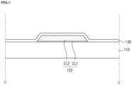
- a gate insulating layer 130 is disposed on the gate line 122, the gate electrode 124 and the sustain line 125.
- the gate insulating layer 130 may include an insulative material, for example, silicon nitride or silicon oxide.
- the gate insulating layer 130 may have a single layer structure or may have a multi-layer structure including two insulating layers having different physical properties.
- the gate insulating layer 130 may prevent electrical connection from being formed between the gate line 122, the gate electrode 124, the sustain line 125, and/or other components disposed thereon.
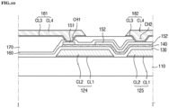
- a semiconductor layer 140 is disposed on the gate insulating layer 130.
- the semiconductor layer 140 overlaps with at least a part of the gate electrode 124.
- the semiconductor layer 140 may include amorphous silicon, polycrystalline silicon or oxide semiconductor.
- the semiconductor layer 140 overlaps with the gate electrode 124, as well as a source electrode 151 and a drain electrode 152, as is described below.
- an ohmic contact element may be additionally disposed on the semiconductor layer 140.
- the ohmic contact element may include n+ hydrogenated amorphous silicon that is highly doped with n-type impurities, or may include silicide.
- a pair of such ohmic contact elements may be disposed on the semiconductor layer 140.
- the ohmic contact element may be disposed between the source electrode 151 and the semiconductor layer 140 and between the drain electrode 152 and semiconductor layer 140, so that the ohmic contact elements may have ohmic contact characteristics.
- the semiconductor layer 140 includes an oxide semiconductor, the ohmic contact element may be omitted.
- the source electrode 151 and the drain electrode 152 are each disposed on the semiconductor layer 140.
- the source electrode 151 may overlap with at least part of the semiconductor layer 140.
- the drain electrode 152 may overlap with at least part of the semiconductor layer 140.
- the source electrode 151 may be spaced apart from the drain electrode 152 by a predetermined distance.
- the source electrode 151 supplies a data voltage from a data line 181 to the semiconductor layer 140.
- the drain electrode 152 supplies the data voltage from the semiconductor layer 140 to the pixel electrode 220.
- the data voltage is applied from an external source and may have a varying voltage level.
- the grey scale of each of the pixels PXs can be controlled by setting the level of the data voltage.
- Each of the source electrode 151 and the drain electrode 152 may include titanium (Ti) and/or molybdenum (Mo).
- the thickness dt2 of the cross section of each of the source electrode 151 and the drain electrode 152 may be less than or equal to half the thickness dt1 of the cross section of each of the gate electrode 124 and the gate line 122.
- the source electrode 151 and the drain electrode 152 may be less than or equal to half the thickness dt3 of the cross section of the data line 181.
- the gate electrode 124, the semiconductor layer 140, the source electrode 151 and the drain electrode 152 form the switching element, e.g., the thin-film transistor 153.
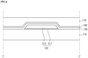
- a first passivation layer 160 is disposed on both the source electrode 151 and the drain electrode 152.
- the first passivation layer 160 may include an inorganic insulating material and may cover the thin-film transistor 153.
- the first passivation layer 160 may protect the thin-film transistor 153 and may prevent materials of a first insulating layer 170 from being introduced into the semiconductor layer 140. In some embodiments, the first passivation layer 160 may be omitted.
- the first insulating layer 170 is disposed on the first passivation layer 160.
- the first insulating layer 170 may include an insulating material and may be an organic layer including, for example, an organic material.
- the first insulation film 170 may reduce height differences created by the elements disposed between the first base substrate 110 and the first insulating layer 170, so as to provide a flat, planar surface. Accordingly, the upper surface of the second insulating layer 170 may be substantially flat.
- the data line 181 and the connection electrode 182 are each disposed on the first insulating layer 170.
- the data line 181 receives the data voltage from an external source to supply the data voltage to the source electrode.
- the data line 181 extends through a first contact hole CH1 formed in the first insulating layer 170 to be electrically connected to the source electrode 151.
- the data line 181 may extend primarily in the second direction D2.
- connection electrode 182 receives the data voltage from the drain electrode 152 and supplies the data voltage to the pixel electrode 220.
- the connection electrode 182 extends through a second contact hole CH2 formed in the first insulating layer 170 to electrically connect the drain electrode 152 with the pixel electrode 220.
- the connection electrode 182 may overlap an area where the second contact hole CH2 is formed.
- the data line 181 and the connection electrode 182 may each include the same material.
- the data line 181 and the connection electrode 182 may have a single layer structure.
- the data line 181 and the connection electrode 182 may each have a multi-layer structure including at least two conductive layers having different physical properties.
- a third conductive layer CL3 disposed at the bottom may include indium zinc oxide (IZO), indium tin oxide (ITO), gallium zinc oxide (GZO), and/or zinc aluminium oxide (ZAO).
- IZO indium zinc oxide
- ITO indium tin oxide
- GZO gallium zinc oxide
- ZAO zinc aluminium oxide
- the above-listed materials are merely illustrative and other materials, such as titanium (Ti), may be used.
- a fourth conductive layer CL4 disposed on the third conductive layer CL3 may include an aluminum-based metal such as aluminum (Al) or an aluminum alloy, a silver-based metal such as silver (Ag) or an silver alloy, a gold-based metal such as gold (Au) or a gold alloy, a copper-based material such as copper (Cu) or a copper alloy, a molybdenum-based metal such as molybdenum (Mo) or a molybdenum alloy, chromium (Cr), tantalum (Ta) and titanium (Ti), etc.
- an aluminum-based metal such as aluminum (Al) or an aluminum alloy
- a silver-based metal such as silver (Ag) or an silver alloy
- a gold-based metal such as gold (Au) or a gold alloy
- a copper-based material such as copper (Cu) or a copper alloy
- a molybdenum-based metal such as molybdenum (Mo) or a molybdenum alloy
- the third conductive layer CL3 fixes the fourth conductive layer CL4 so that it is not easily separated from the first insulating layer 170, the source electrode 151 and the drain electrode 152, and also works as a passage through which the data voltage is transferred.
- the fourth conductive layer CL4 works as a passage through which the data voltage is mainly transferred.
- the cross section of the fourth conductive layer CL4 may be thicker than the cross section of the third conductive layer CL3.
- the thickness dt3 of the cross section of each of the data line 181 and the connection electrode 182 is larger than the thickness dt2 of the cross section of each of the source electrode 151 and the drain electrode 152.
- the thickness dt2 of the cross section of each of the source electrode 151 and the drain electrode 152 is smaller than the thickness dt3 of the cross section of each of the data line 181 and the connection electrode 182.
- the thickness dt2 of the cross section of each of the source electrode 151 and the drain electrode 152 is less than or equal to half the thickness dt3 of the cross section of each of the data line 181 and the connection electrode 182.
- the charging rate which represents how much the initially supplied data voltage is transferred to the pixel electrode 220, is increased.
- a second passivation layer 190 is disposed on the data line 181 and the connection electrode 182.
- the second passivation layer 190 may include an inorganic insulating material and may cover the data line 181 and the connection electrode 182.
- the second passivation layer 190 may protect the data line 181 and the connection electrode 182 and prevent the material of a second insulating layer 210 or a color filter layer 200 from infiltrating into a layer where the data line 181 and the connection electrode 182 are disposed.
- the second passivation layer 190 may be omitted.
- the colour filter layer 200 is disposed on the second passivation layer 190.
- the colour filter layer 200 may be a photosensitive organic composition containing a pigment for reproducing a colour and may include at least one of a red, green or blue pigment. It is to be understood that the colours of the pigments are not limited to red, green and blue.
- the second insulating layer 210 is disposed on the colour filter layer 200.
- the second insulating layer 210 may include an insulating material and may be an organic layer including an organic material, for example.
- the second insulating layer 210 like the first insulating layer 170, may reduce height differences created by the elements disposed between the first base substrate 110 and the second insulating layer 210, to provide a flat surface. Accordingly, the upper surface of the second insulating layer 210 may be substantially flat.
- the pixel electrode 220 is disposed on the second insulating layer 210.
- the pixel electrode 220 may extend through a third contact hole CH3 formed in the second insulating layer 210 to be electrically connected to the connection electrode 182.
- the pixel electrode 220 may receive the data voltage from the connection electrode 182.
- the pixel electrode 220 may include a transparent conductive material such as indium tin oxide (ITO), indium zinc oxide (IZO), indium tin zinc oxide (ITZO), Al-doped zinc oxide (AZO).
- ITO indium tin oxide
- IZO indium zinc oxide
- ITZO indium tin zinc oxide
- AZO Al-doped zinc oxide
- the pixel electrode 220 may be disposed primarily in the active area ACA but may additionally be disposed in an area that extends to overlap the third contact hole CH3 for connection with the connection electrode 182, for example, an extension electrode 224.
- the pixel electrode 220 may include slits which are opened portions where no transparent conductive material is disposed. By virtue of the slits SL, a regular pattern is formed in the pixel electrode 220. The direction and degrees that the liquid crystals LC above the pixel electrode 220 are tilted may be controlled by the shape and the pattern of the pixel electrode 220.
- the pixel electrode 220 includes first stem electrodes 221, a second stem electrode 222, branch electrodes 222, and an extension electrode 224.
- the extension electrode 224 may be disposed outside of the active area ACA.
- the first stem electrodes 221 may extend along the first direction D1 in the active area ACA. Although one pixel PX includes two first stem electrodes 221, in the configuration shown in FIG. 2 , the number of the first stem electrodes 221 may be different in some exemplary embodiments of the present.
- the second stem electrode 222 may be extended in the second direction D2 in the active area ACA. As the first stem electrodes 221 are extended in the first direction D1 in the active area ACA and the second stem electrode 222 is extended in the second direction D2 in the active area ACA, the first stem electrodes 221 and the second stem electrode 222 may intersect each other. Although one pixel PX includes one second stem electrode 222 in the configuration shown in FIG. 2 , the number of the second stem electrode 222 may be different in some exemplary embodiments of the present invention.
- the plurality of branch electrodes 223 may be disposed in the active area ACA and may extend from the first stem electrodes 221 or the second stem electrode 222. Generally, the branch electrodes 223 may be extended away from the intersections between the first stem electrodes 221 and the second stem electrode 222.
- the slits SL may correspond to opened portions between the first stem electrodes 221 and the branch electrodes 223 and between the second stem electrode 222 and the branch electrodes 223.
- the extension electrode 224 may be extended from some of the branch electrodes 223 and may be extended beyond the active area ACA.
- the extension electrode 224 may be disposed out of the active area ACA such that the extension electrode 224 overlaps with the third contact hole CH3 formed in the second insulating layer 210.
- the extension electrode 224 may conform to the shape of the side walls of the third contact hole CH3.
- the pixel electrode 220 may receive the data voltage from the connection electrode 182 via the extension electrode 224.
- a first alignment layer may be additionally disposed on the pixel electrode 220.
- the first alignment layer may control an initial orientation angle of the liquid crystals LC injected into the liquid-crystal layer LCL.
- a light blocking element 230 may be disposed on the pixel electrode 220.
- the light blocking element 230 may overlap a part of the gate line 122, the data line 181, the first contact hole CH1 and the thin-film transistor 153.
- the light blocking element 230 may block incident light from the first base substrate 110. Further, by the various components on the first base substrate 110 that contain metal materials which do not transmit light as well as the light blocking element 230, the transmission of light in areas other than the active area ACA can be blocked.
- a spacer 240 is disposed on the light blocking element 230.
- the spacer 240 may maintain the gap between the first display substrate SUB1 and the second display substrate SUB2. In some exemplary embodiments of the present invention, the spacer 240 may overlap at least a part of the thin-film transistor 153.
- the source electrode 151 and the data line 181 are separated from each other and are electrically connected to each other only via a first contact hole CH1.
- the drain electrode 152 and the connection electrode 182 are separated from each other and are electrically connected to each other only via a second contact hole CH2.
- the first insulating layer 170 is disposed between the gate electrode 124 and the data line 181, and the first insulating layer 170 is disposed between the gate electrode 124 and the connection electrode 182, such that the distance between the gate electrode 124 and the data line 181 is increased, and the distance between the gate electrode 124 and the data connection electrode 182 is also increased. Accordingly, the capacitance between the gate electrode 124 and the data line 181 may be reduced, and the capacitance between the gate electrode 124 and the connection electrode 182 may be reduced.
- the dielectric constant of the first insulating layer 170 is lower than that of the gate electrode 124, the data line 181 and the connection electrode 182, the dielectric constant is reduced, such that capacitance between the gate electrode 124 and the data line 181 can be reduced, and the capacitance between the gate electrode 124 and the connection electrode 182 can be reduced. Accordingly, the RC delay of the data voltage supplied through the data line 181 and the connection electrode 182 decreases, and thus the charging rate can be increased. As the charging rate is increased, the display quality of the display device can be increased.
- the data line 181 and the connection electrode 182 are each disposed on the substantially flat upper surface of the first insulating layer 170, and thus the gate electrode 124, the gate line 122, the data line 181 and the connection electrode 182 all can be formed relatively thick (e.g., as measured in cross section). As a result, the resistance can be reduced.
- the first insulating layer 170 provides the flat surface for the data line 181 and the connection electrode 182
- the risk that the data line 181 and the connection electrode 182 are damaged, such as by cracks, may be reduced, and it is possible to reduce the resistance by forming the data line 181 and the connection electrode 182 to be relatively thick.
- the resistance of the gate electrode 124, the data line 181 and the connection electrode 182 can be reduced, and the RC delay of the data voltage, which is provided through the data line 181 and the connection electrode 182, can be reduced.
- the charging rate can be increased.
- the display quality of the display device can be increased.
- the source electrode 151 and the data line 181 may include different materials and may be formed in different layers.
- the drain electrode 152 and the connection electrode 182 may include different materials and may be formed in different layers, such that the channel length of the thin-film transistor 153 can be reduced.
- the channel length is defined as a distance between the drain electrode 152 and the source electrode 151 of the thin-film transistor 153. The shorter the channel length is, the better the data voltage is transferred from the source electrode 151 to the drain electrode 152, and thus the charging rate can be increased. For example, when the thickness of the cross-section of the source electrode 151 and the drain electrode 152 is increased, the distance between the source electrode 151 and the drain electrode 152 is increased in order to increase the margin between the two electrodes.
- the channel length may become longer.
- the thickness of the cross-section of the source electrode 151 and the drain electrode 152 is relatively thin, so that the margin can be reduced and the channel length can become shorter.
- the data line 181 and the source electrode 151 are formed in different layers, and the connection electrode 182 and the drain electrode 152 are formed in different layers, so that the thickness of the cross section of the data line 181 and the drain electrode 152 become thick while the channel length can be reduced, to thereby increase the charging rate and the display quality of the display device.
- the second display substrate SUB2 includes the second base substrate 310 and the common electrode 320.
- the second base substrate 310 may be disposed such that it faces the first base substrate 110.
- the second base substrate 310 may be highly durable so that it can withstand external impact.
- the second base substrate 310 may be a transparent insulation substrate.
- the second base substrate 310 may be a glass substrate, a quartz substrate, a transparent resin substrate, etc.
- the second base substrate 310 may be a flat plate, the present invention is not limited to this particular arrangement. It is to be understood that the second base substrate 310 may be curved in a particular direction.
- the common electrode 320 is disposed on the surface of the second base substrate 310 that faces the first display substrate SUB1.
- the common electrode 320 may include a transparent conductive material such as indium tin oxide (ITO), indium zinc oxide (IZO), indium tin zinc oxide (ITZO) and/or Al-doped zinc oxide (AZO).
- ITO indium tin oxide
- IZO indium zinc oxide
- ITZO indium tin zinc oxide
- AZO Al-doped zinc oxide
- the common electrode 320 may be formed throughout the entire surface of the second base substrate 310 as a single, continuous plate.
- the common electrode 320 may receive a common signal from an external source and may form an electric field across the liquid-crystal layer LCL together with the pixel electrode 220.
- the common signal may be supplied from an external source, and the voltage level of the common signal may be kept constant while the LCD device is driven. Accordingly, electric field may be formed between the pixel electrode 220 and the common electrode 320 overlapping each other due to a height difference between the data voltage supplied to the pixel electrode 220 and the common voltage supplied to the common electrode 320.
- the liquid crystals LC may be rotated or tilted by the electric field.
- a second alignment layer may be disposed on the surface of the common electrode 320 that faces the first display substrate SUB1. Similar to the first alignment layer, the second alignment layer may control the initial orientation angle of the liquid crystals LC injected into the liquid-crystal layer LCL.
- liquid-crystal layer LCL will be described.
- the liquid-crystal layer LCL may include liquid crystals LC having dielectric anisotropy and refractive anisotropy.
- the liquid crystals LC may be aligned vertically with respect to the first display substrate SUB1 and the second display substrate SUB2 when no electric field is applied.
- the liquid crystals LC may be rotated or tilted in a particular direction between the first display substrate SUB1 and the second display substrate SUB2 to thereby change the polarization of light.
- the vertically-aligned LCD device has been described with reference to FIGS. 2 and 3 where the liquid crystals LC are initially orientated in the direction perpendicular to the first display substrate SUB1 and the second display substrate SUB2, the technical idea of the present disclosure is not limited thereto.
- the cross sectional structure including the first insulating layer 170 may be equally applied to a horizontally-aligned LCD device where liquid crystals LC are initially orientated in parallel with the surface of the first display substrate SUB1 and the second display substrate SUB2. Also in this case, it is possible to achieve the effect of increasing the charging rate and accordingly increasing the display quality.
- FIGS. 4 to 11 are cross-sectional views showing processing steps of a method of manufacturing the display panel shown in FIGS. 2 and 3 .
- FIGS. 4 , 6 , 8 and 10 are cross-sectional views taken along line I - I' of FIG. 2 .
- FIGS. 5 , 7 , 9 and 11 are cross-sectional views taken along line II - II' of FIG. 2 .
- a gate line 122, a gate electrode 124 and a sustain line 125 are formed on a first base substrate 110.
- the gate line 122, the gate electrode 124 and the sustain line 125 may include a same material and may each have a multi-layer structure including a first conductive layer CL1 and a second conductive layer.
- the thickness of the cross section of the gate line 122, the gate electrode 124 and the sustain lines 125 may range from approximately 5,000 A to 20,000 ⁇ .
- the first conductive layer CL1 may include indium zinc oxide (IZO), indium tin oxide (ITO), gallium zinc oxide (GZO) and/or zinc aluminum oxide (ZAO) and may have a cross-sectional thickness of approximately 100 ⁇ to 1,000 ⁇ .
- the second conductive layer CL2 may include an aluminum-based metal such as aluminum (Al) or an aluminum alloy, a silver-based metal such as silver (Ag) or a silver alloy, a gold-based metal such as gold (Au) or a gold alloy, a copper-based material such as copper (Cu) or a copper alloy, a molybdenum-based metal such as molybdenum (Mo) or an molybdenum alloy, chromium (Cr), tantalum (Ta) and titanium (Ti), and may have a thickness of approximately 5,000 ⁇ to 20,000 ⁇ .
- aluminum-based metal such as aluminum (Al) or an aluminum alloy
- a silver-based metal such as silver (Ag) or a silver alloy
- a gold-based metal such as gold (Au) or a gold alloy
- a copper-based material such as copper (Cu) or a copper alloy
- a molybdenum-based metal such as molybdenum (Mo) or an moly
- the gate line 122, the gate electrode 124 and the sustain line 125 are stacked by sputtering, chemical vapor deposition (CVD), plasma enhanced chemical vapor deposition (PECVD), etc. and may be formed by patterning.
- CVD chemical vapor deposition
- PECVD plasma enhanced chemical vapor deposition
- the photoresist composition is exposed to light so that it has a pattern conforming to the shapes of the gate line 122, the gate electrode 124 and the sustain line 125. Subsequently, the two metal layers are etched sequentially to form the gate line 122, the gate electrode 124 and the sustain line 125.
- a gate insulating layer 130, a semiconductor layer 140 disposed on the gate insulating layer 130, a source electrode 151 and a drain electrode 152 disposed on the semiconductor layer 140 are sequentially formed.
- the gate insulating layer 130 may include an inorganic insulating material as described above.
- the semiconductor layer 140 is formed on the gate insulating layer 130.
- the semiconductor layer 140 may include amorphous silicon, polycrystalline silicon or oxide semiconductor.
- the source electrode 151 and the drain electrode 152 disposed on the semiconductor layer 140 may be simultaneously formed using the same mask as is used to form the semiconductor layer 140.
- a metal layer forming the source electrode 151 and the drain electrode 152 is stacked on the semiconductor material layer.
- a photoresist composition is applied onto the metal layer, and then exposure is performed with a slit mask such that the photoresist composition has the largest thickness where the source electrode 151 and the drain electrode 152 are disposed, has a relatively small thickness where the channel is formed, and is entirely removed in the rest of the area.
- the metal layers and the semiconductor material layer are sequentially etched, such that the source electrode 151, the drain electrode 152 and the semiconductor layer 140 can be formed.
- the thickness of the cross section of the source electrode 151 and the drain electrode 152 range from 500 ⁇ to 2,000 ⁇ .
- a source electrode 151, a first passivation layer 160 disposed on the source electrode 151, and a first insulating layer 170 disposed on the first passivation layer 160 are sequentially formed.
- a first passivation material layer including a constituent material for the first passivation layer 160 is stacked on the source electrode 151 and the drain electrode 152. Then, a first insulating material layer including an organic material for the first insulating layer 170 is stacked on the first passivation material layer.
- Exposure is performed on the stacked first passivation material layer and the first insulating material layer with a mask having a pattern conforming to the first contact hole CH1 and the second contact hole CH2, and then first contact hole CH1 and the second contact hole CH2 are formed, such that the first passivation layer 160 and the first insulating layer 170 can be formed.
- a data line 181 and a connection electrode 182 are formed on the first insulating layer 170.
- the data line 181 and the connection electrode 182 may include the same material as described above, and may have a multi-layer structure including a third conductive layer CL3 and a fourth conductive layer CL4.
- the thickness of the cross section of the data line 181 and the connection electrode 182 range from 5,000 ⁇ to 20,000 ⁇ .
- the third conductive layer CL3 may include indium zinc oxide (IZO), indium tin oxide (ITO), gallium zinc oxide (GZO), and/or zinc aluminum oxide (ZAO) and may have a cross-sectional thickness of approximately 100 ⁇ to 1,000 ⁇ .
- the fourth conductive layer CL4 may be made up of an aluminum-based metal such as aluminum (Al) or an aluminum alloy, a silver-based metal such as silver (Ag) or a silver alloy, a gold-based metal such as gold (Au) or a gold alloy, a copper-based metal such as copper (Cu) or a copper alloy, a molybdenum-based metal such as molybdenum (Mo) or an molybdenum alloy, chromium (Cr), tantalum (Ta) and titanium (Ti), and may have a thickness of approximately 5,000 ⁇ to 20,000 ⁇ .
- an aluminum-based metal such as aluminum (Al) or an aluminum alloy
- a silver-based metal such as silver (Ag) or a silver alloy
- a gold-based metal such as gold (Au) or a gold alloy
- a copper-based metal such as copper (Cu) or a copper alloy
- a molybdenum-based metal such as molybdenum (Mo)
- the data line 181 and the connection electrode 182 are stacked by sputtering, chemical vapor deposition (CVD), plasma enhanced chemical vapor deposition (PECVD), etc. and may be formed by patterning.
- CVD chemical vapor deposition
- PECVD plasma enhanced chemical vapor deposition
- the photoresist composition is exposed to light so that the photoresist composition has a pattern conforming to the shapes of the data line 181 and the connection electrode 182. Subsequently, the two metal layers are etched sequentially to form the data line 181 and the connection electrode 182.
- a color filter layer 200, a second insulating layer 210, a pixel electrode 220, a light blocking element 230 and a spacer 240 are formed so that a display panel having the structure shown in FIG. 3 can be manufactured.
- FIG. 12 is a cross-sectional view illustrating a pixel of a display panel according to an exemplary embodiment of the present disclosure, taken along line I - I' of FIG. 2 .
- the cross-sectional view of the display panel illustrated in FIG. 12 may be different from the cross-sectional view of the display panel shown in FIG. 3 in that the former further includes a reinforcing layer 111. Therefore, descriptions will be focused on differences, and the redundant description will be omitted. It may be assumed that any omitted details are similar to or the same as corresponding details described above with respect to FIG. 3 .
- a pixel PX of the display panel includes a first display substrate SUB1_a, a second display substrate SUB2, and a liquid-crystal layer LCL.
- the first display substrate SUB1_a includes a first base substrate 110, an reinforcing layer 111_a, a gate line 122, a gate electrode 124, a sustain line 125, a gate insulating layer 130, a semiconductor layer 140, a source electrode 151, a drain electrode 152, a first passivation layer 160, a first insulating layer 170, a data line 181, a connection electrode 182, a second passivation layer 190, a color filter layer 200, a second insulating layer 210, a pixel electrode 220, a light blocking element 230, and a spacer 240.
- the reinforcing layer 111_a is disposed on the first base substrate 110.
- the reinforcing layer 111 may be implemented as a thin film including silicon nitride (SiNx).
- the reinforcing layer 111_a may have a higher strength than the first base substrate 110 and may reduce or prevent the deformation of the first base substrate 110 that may occur in the process of forming various components on the reinforcing layer 111_a.
- the degrees of deformation of the elements may differ from the degree of deformation of the first base substrate 110, such that the first base substrate 110 may be bent. This bending may be prevented by additionally including the reinforcing layer 111_a.
- FIG. 13 is a cross-sectional view illustrating a pixel of a display panel according to an exemplary embodiment of the present disclosure, taken along line I - I' of FIG. 2 .
- the cross-sectional view of the display panel according to FIG. 13 is different from the cross-sectional view of the display panel shown in FIG. 12 in that a reinforcing layer 111_b is located at a different position. Therefore, descriptions will be focused on differences, and the redundant description will be omitted. It may be assumed that any omitted details are similar to or the same as corresponding details described above with respect to the prior figures.
- a pixel PX of the display panel includes a first display substrate SUB1_b, a second display substrate SUB2, and a liquid-crystal layer LCL.
- the first display substrate SUB1_b includes a first base substrate 110, an reinforcing layer 111_b, a gate line 122, a gate electrode 124, a sustain line 125, a gate insulating layer 130, a semiconductor layer 140, a source electrode 151, a drain electrode 152, a first passivation layer 160, a first insulating layer 170, a data line 181, a connection electrode 182, a second passivation layer 190, a color filter layer, a second insulating layer 210, a pixel electrode 220, a light blocking element 230, and a spacer 240.
- reinforcing layer 111_b might be different from those elements described above with reference to FIG. 3 ; and, therefore, the redundant description will be omitted.
- the reinforcing layer 111_b is disposed on the first base substrate 110.
- the reinforcing layer 111_b is formed on a surface of the first base substrate 110 that is opposed to the surface facing the first base substrate 110 on which the gate line 122, the gate electrode 124k the sustain line 125, etc. are disposed.
- the reinforcing layer 111_b may be implemented as a thin film including silicon nitride (SiNx).
- the reinforcing layer 111_b may have a higher strength than the first base substrate 110 and may reduce or prevent the deformation of the first base substrate 110 that may occur in the process of forming various components on the reinforcing layer 111_b. That is, the reinforcing layer 111_b may include the same material as the reinforcing layer 111_a in FIG. 12 included in the display panel according to the configuration shown in FIG. 12 , and may perform the same functionality.
- FIG. 14 is a cross-sectional view illustrating a pixel of a display panel according to an exemplary embodiment of the present disclosure, taken along line I - I' of FIG. 2 .
- the cross-sectional view of the display panel illustrated in FIG. 14 is different from the cross-sectional views of the display panels shown in FIGS. 12 and 13 in that a plurality of reinforcing layers 111_c is formed. Therefore, descriptions will be focused on differences, and the redundant description will be omitted. It may be assumed that any omitted details are similar to or the same as corresponding details described above with respect to the prior figures.
- a pixel PX of the display panel includes a first display substrate SUB1_c, a second display substrate SUB2, and a liquid-crystal layer LCL.
- the first display substrate SUB1_c includes a first base substrate 110, reinforcing layers 111_c, a gate line 122, a gate electrode 124, a sustain line 125, a gate insulating layer 130, a semiconductor layer 140, a source electrode 151, a drain electrode 152, a first passivation layer 160, a first insulating layer 170, a data line 181, a connection electrode 182, a second passivation layer 190, a color filter layer, a second insulating layer 210, a pixel electrode 220, a light blocking element 230, and a spacer 240.
- One of the reinforcing layers 111_c is disposed on a surface of the first base substrate 110, and the other of the reinforcing layers 111_c is disposed on an opposed surface of the first base substrate 110.
- the reinforcing layers 111_c are disposed on both surfaces of the first base substrate 110.
- the reinforcing layers 111_c may be implemented as a thin film including silicon nitride (SiNx).
- the reinforcing layers 111_c may have a higher strength than the first base substrate 110 and may reduce or prevent the deformation of the first base substrate 110 that may occur in the process of forming various components on the reinforcing layers 111_c.
- the reinforcing layers 111_c may include the same material as the reinforcing layer 111_a in FIG. 12 included in the display panel shown in FIG. 12 , and may perform the same functionality.
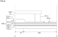
- FIG. 15 is a cross-sectional view of a display panel according to an exemplary embodiment of the present disclosure, taken along line III - III' of FIG. 1 .
- FIG. 15 shows a portion of the end of the display area DA and the non-display area NDA.
- the display panel includes a first display substrate SUB1, a second display substrate SUB2 and a liquid-crystal layer LCL.
- the first display substrate SUB1 includes a first base substrate 110, a pad line 126, a gate insulating layer 130, a first passivation layer 160, a first insulating layer 170, a second passivation layer 190, a second insulating layer 210, a sealant 250, and a pad electrode 260.
- the first base substrate 110 may be identical to that of FIG. 3 ; and, therefore, the redundant description will be omitted. It may be assumed that any omitted details are similar to or the same as corresponding details described above with respect to the prior figures.
- the pad line 126 is disposed on the first base substrate 110.
- the pad line 126 may include the same material as the gate line 122, the gate electrode 124 and the sustain line 125, and may be formed in the same layer. Accordingly, the pad line 126 may have a multi-layer structure including the first conductive layer CL1 and the second conductive layer CL2.
- the pad line 126 may be electrically connected to the gate line 122 or the data line 181 in the display area DA to transfer the gate voltage or the data voltage supplied from an external source to the gate line 122 or the data line 181, respectively. Accordingly, the pad line 126 may be disposed to extend to the non-display area NDA.
- the gate insulating layer 130 is disposed on the pad line 126.
- the gate insulating layer 130 may be disposed to overlap the non-display area NDA. It may be assumed that the other features of the gate insulating layer 130 are similar to or the same as corresponding details described above with respect to FIG. 3 .
- a first passivation layer 160 is disposed on the gate insulating layer 130.
- the first passivation layer 160 may be disposed to overlap the non-display area NDA. It may be assumed that the other features of the gate first passivation layer 160 are similar to or the same as corresponding details described above with respect to FIG. 3 .
- the first insulating layer 170 is disposed on the first passivation layer 160.
- the first insulating layer 170 may overlap with the display area DA and a relatively small part of the non-display area NDA.
- the area where the first insulating layer 170 overlaps with the non-display area NDA may be smaller than the area where the first passivation layer 160 overlaps with the non-display area NDA. It may be assumed that the other features of the first insulating layer 170 are similar to or the same as corresponding details described above with respect to FIG. 3 .
- the second passivation layer 190 is disposed on the first insulating layer 170.
- the second passivation layer 190 may be disposed to overlap the non-display area NDA. It may be assumed that the other features of the second passivation layer 190 are similar to or the same as corresponding details described above with respect to FIG. 3 .
- the second insulating layer 210 is disposed on the second passivation layer 190.
- the second insulating layer 210 may be disposed to overlap the non-display area NDA.
- the thickness of the cross section of the second insulating layer 210 may decrease gradually from the display area DA to the non-display area NDA. It may be assumed that the other features of the second insulating layer 210 are similar to or the same as corresponding details described above with respect to FIG. 3 .
- the sealant 250 is disposed on the second insulating layer 210.
- the sealant 250 may seal the liquid crystals LC of the liquid-crystal layer LCL disposed between the first display substrate SUB1 and the second display substrate SUB2 so that the liquid crystals LC do not leak from their area.
- the pixel electrode 260 is disposed on the second insulating layer 210.
- the pad electrode 260 may include a conductive metal and may be electrically connected to the pad line 126 through a fourth contact hole CH4 that penetrates all the elements between the second insulating layer 210 and the gate insulating layer 130.
- the pad electrode 260 may receive various signals (for example, the data voltage or the gate voltage) supplied from an external source to the display panel, and provide it to the pad line 126.
- FIG. 16 is a cross-sectional view illustrating a display panel according to an exemplary embodiment of the present disclosure, taken along line III - III' of FIG. 1 .
- the cross-sectional view of the display panel according to this figure is different from the cross-sectional view of the display panel shown in FIG. 15 in that a pad electrode 260 is located at a different position. Therefore, descriptions will be focused on differences, and the redundant description will be omitted.
- the display panel includes a first display substrate SUB1_d, a second display substrate SUB2 and a liquid-crystal layer LCL.
- the first display substrate SUB1_d includes a first base substrate 110, a pad line 183_d, a gate insulating layer 130_d, a first passivation layer 160_d, a first insulating layer 170_d, a second passivation layer 190_d, a second insulating layer 210_d, a sealant 250_d, and a pad electrode 260_d.
- the pad line 183_d may be disposed on the first insulating layer 170_d. Accordingly, when the pad line 183_d is made up of multiple layers, it may include the third conductive layer CL3 and the fourth conductive layer CL4. In addition, as the pad line 183_d is disposed on the first insulating layer 170_d, the features disposed under the pad line 183_d (e.g., the first passivation layer 160_d, and the gate insulating layer 130_d) may overlap with the non-display area NDA.
- the pad line 183_d is disposed on the first insulating layer 170_d, the thickness of the cross section of the liquid-crystal layer LCL disposed at the boundary between the display area DA and the non-display area NDA can be received. Accordingly, it is possible to prevent misalignment of the liquid crystals LC in the liquid-crystal layer LCL disposed at the boundary between the display area DA and the non-display area NDA, and thus light leakage can be suppressed.
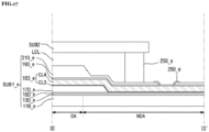
- FIG. 17 is a cross-sectional view illustrating a display panel according to an exemplary embodiment of the present disclosure, taken along line III - III' of FIG. 1 .
- the cross-sectional view of the display panel according to this approach is different from the cross-sectional view of the display panel shown in FIG. 15 in that a first insulating layer 170_e is located at a different position. Therefore, descriptions will be focused on differences, and the redundant description will be omitted.
- the display panel includes a first display substrate SUB1_e, a second display substrate SUB2 and a liquid-crystal layer LCL.
- the first display substrate SUB1_e includes a first base substrate 110, a pad line 183_e, a gate insulating layer 130_e, a first passivation layer 160_e, a first insulating layer 170_e, a second passivation layer 190_de a second insulating layer 210_e, a sealant 250_e, and a pad electrode 260_e.
- the pad line 183_e is disposed on the first insulating layer 170_e but the area where the first insulating layer 170_e disposed under the first insulating layer 170_e overlaps with the non-display area NDA can be reduced.
- the first insulating layer 170_e may overlap with the display area DA and a relatively small part of the non-display area NDA.
- the area where the first insulating layer 170_e overlaps with the non-display area NDA may be smaller than the area where the first passivation layer 160_e overlaps with the non-display area NDA.
- the pad line is disposed on the first insulating layer 170_e, the first insulating layer 170_e may have the same structure as shown in FIG. 15 .
Landscapes
- Physics & Mathematics (AREA)
- Nonlinear Science (AREA)
- Engineering & Computer Science (AREA)
- Mathematical Physics (AREA)
- Chemical & Material Sciences (AREA)
- Crystallography & Structural Chemistry (AREA)
- General Physics & Mathematics (AREA)
- Optics & Photonics (AREA)
- Microelectronics & Electronic Packaging (AREA)
- Manufacturing & Machinery (AREA)
- Devices For Indicating Variable Information By Combining Individual Elements (AREA)
- Liquid Crystal (AREA)
Description
- The present disclosure relates to a display panel and a display device having the same.
- A display device is a device that includes a display panel. Display panels generally include a plurality of pixels. Display panels may be of various types such as a liquid-crystal display device (LCD device) and an organic light-emitting diode display (OLED display device), etc.
- Particularly, a liquid-crystal display panel, which is used in a liquid-crystal display device, is composed of two substrates on which electric field generating electrodes, such as pixel electrodes and common electrodes, are formed. A liquid-crystal layer is injected between the two substrates. Voltage is applied to the electric field generating electrodes to form an electric field across the liquid-crystal layer. As a result of the electric field, the orientation of the liquid crystals contained in the liquid-crystal layer is aligned and the polarization of incident light is controlled, thereby displaying an image.
- The pixel electrode is connected to a switching device such as a thin-film transistor (TFT) and receives a data voltage corresponding to a video signal input to the display panel.
-
US2011084268 discloses a semiconductor device where a wiring with low resistance is connected to a thin film transistor in which a source electrode and a drain electrode connected to an oxide semiconductor layer with a suppressed impurity concentration. In addition, the thin film transistor including the oxide semiconductor may be surrounded by insulating films to be sealed. - According to an aspect of the invention, there is provided a display panel as set out in claim 1. Optional features are set out in the dependent claims.
- The above and other aspects and features of the present disclosure will become more apparent by describing in detail exemplary embodiments thereof with reference to the attached drawings, in which:
-
FIG. 1 is a perspective view illustrating a display panel according to an exemplary embodiment of the present disclosure; -
FIG. 2 is a layout diagram illustrating a single pixel disposed in a display panel according to an exemplary embodiment of the present disclosure; -
FIG. 3 is a cross-sectional view taken along line I - I' ofFIG. 2 ; -
FIGS. 4 to 11 are cross-sectional views illustrating processing steps of a method of manufacturing the display panel shown inFIGS. 2 and3 ; -
FIG. 12 is a cross-sectional view illustrating a pixel of a display panel according to an exemplary embodiment of the present disclosure, taken along line I - I' ofFIG. 2 ; -
FIG. 13 is a cross-sectional view illustrating a pixel of a display panel according to an exemplary embodiment of the present disclosure, taken along line I - I' ofFIG. 2 ; -
FIG. 14 is a cross-sectional view illustrating a pixel of a display panel according to an exemplary embodiment of the present disclosure, taken along line I - I' ofFIG. 2 ; -
FIG. 15 is a cross-sectional view illustrating a display panel according to an exemplary embodiment of the present disclosure, taken along line III - III' ofFIG. 1 ; -
FIG. 16 is a cross-sectional view illustrating a display panel according to an exemplary embodiment of the present disclosure, taken along line III - III' ofFIG. 1 ; and -
FIG. 17 is a cross-sectional view illustrating a display panel according to yet another exemplary embodiment of the present disclosure, taken along line III - III' ofFIG. 1 . - In describing exemplary embodiments of the present disclosure illustrated in the drawings, specific terminology is employed for sake of clarity. However, the present disclosure is not intended to be limited to the specific terminology so selected, and it is to be understood that each specific element includes all technical equivalents which operate in a similar manner.
- As used herein, an electronic apparatus may be any apparatus that includes a display device. Examples of the electronic apparatus may include smart phones, mobile phones, wearable devices such as smart watches, turn-by-turn navigation systems, video game consoles, TVs, car head units, notebook computers, laptop computers, tablet computers, personal media players (PMPs), and personal digital assistants (PDAs). The electronic apparatus may be embodied as a pocket-sized portable communication terminal having a wireless communication function. Further, the display device may be a flexible display device capable of being bent into an orientation other than flat.
- Hereinafter, exemplary embodiments of the present invention will be described with reference to the attached drawings.
-
FIG. 1 is a perspective view illustrating a display panel according to an exemplary embodiment of the present disclosure. - Referring to
FIG. 1 , a display panel, according to an exemplary embodiment of the present disclosure, includes a first display substrate SUB1 and a second display substrate SUB2. The second display substrate SUB2 has a smaller area than the first display substrate SUB1. - The second display substrate SUB2 overlaps with the first display substrate SUB1. Liquid crystals LC are injected into a space between the first display substrate SUB1 and the second display substrate SUB2 to form a liquid-crystal layer LCL between the first display substrate SUB1 and the second display substrate SB2.
- A surface of the first display substrate SUB1 that faces the second display substrate SUB2 may be divided into a display area DA and a non-display area NDA. The display area DA may be defined as an area where a plurality of pixels PXs for displaying an image is disposed. Accordingly, an image to be displayed may be displayed entirely within the display area DA. The non-display area NDA may be defined as the area of the first display substrate SUB1 that is not the display area DA.
- The display area DA may be disposed entirely within an area where the first display substrate SUB1 and the second display substrate SUB2 overlap. For example, the second display substrate SUB2 may fully correspond to the display area DA of the first substrate SUB1 or the second display substrate SUB2 may cover a portion of the non-display area NDA as well as an entirety of the display area DA. The plurality of pixels PXs may be arranged in a matrix pattern along the first direction D1 and the second direction D2, which may be substantially perpendicular to each other. In an exemplary embodiment of the present disclosure, the pixels PXs may include first to third pixel types representing red color, green color and blue color pixels, respectively. In some exemplary embodiments of the present disclosure, the pixels PXs may include yellow color, cyan color, and a magenta color pixels, respectively. Furthermore, the pixels PXs may include white pixels for displaying white as well.
- The gray scale of each pixel PX may be individually controlled. Each of the pixels PX may work as a unit for displaying a particular color. The grayscale of each of the pixels PXs can be controlled by adjusting the amount of incident light that travels from below the first display substrate SUB1 toward the second display substrate SUB2.
- Various components for driving the pixels PXs, such as a drive IC may be mounted in the non-display area NDA.
- Display devices include liquid-crystal display devices, organic light-emitting display device, etc. and each type of display device may have a unique structure of the pixels PXs. In the following description, it is assumed that the display device is a liquid-crystal display device. However, it is to be noted that the technical idea of exemplary embodiments of the present disclosure may equally applied to organic light-emitting display device as well.
- The structure of each of the pixels PXs will be described in detail with reference to
FIGS. 2 and3 . -
FIG. 2 is a layout diagram illustrating a single pixel disposed in a display panel according to an exemplary embodiment of the present disclosure.FIG. 3 is a cross-sectional view taken along line I - I' ofFIG. 2 . - Referring to
FIGS. 2 and3 , one pixel PX of the display panel, according to an exemplary embodiment of the present disclosure, includes a first display substrate SUB1, a second display substrate SUB2, and a liquid-crystal layer LCL. Each of the pixels PXs includes an active area ACA through which light is transmitted. - Various components for changing the orientation of the liquid crystals LC in the liquid-crystal layer LCL, such as a
pixel electrode 220 and a thin-film transistor 153 may be disposed on the first display substrate SUB1. - The second display substrate SUB2 faces the first display substrate SUB1. On the second display substrate SUB2, a
common electrode 320 is disposed on asecond base substrate 310 so as to face thepixel electrode 220. - The liquid-crystal layer LCL is interposed between the first display substrate SUB1 and the second display substrate SUB2 and may include liquid crystals LC having dielectric anisotropy. When electric field is applied across the first display substrate SUB1 and the second display substrate SUB2, the liquid crystals LC may be rotated in a particular direction between the first display substrate SUB1 and the second display substrate SUB2 to thereby change the polarization of light passing therethrough. Herein, the term rotation may refer not only to actual rotation of the liquid crystals LC but also to any change in orientation of the liquid crystals LC caused by the electric field.
- Hereinafter, the first display substrate SUB1 will be described.
- The first display substrate SUB1 includes a
first base substrate 110. Thefirst base substrate 110 may be a transparent insulation substrate. For example, thefirst base substrate 110 may be a glass substrate, a quartz substrate, a transparent resin substrate, etc. - According to some exemplary embodiments of the present invention, the
first base substrate 110 may be curved in a particular direction. In some exemplary embodiments of the present invention, thefirst base substrate 110 may be flexible. For example, thefirst base substrate 110 may be deformable so that it may be rolled, folded, bent and so on. - A
gate line 122, agate electrode 124 and a sustainline 125 are each disposed on thefirst base substrate 110. - The
gate line 122 transfers a gate voltage for controlling the thin-film transistor 153. Thegate line 122 may be extended in a first direction D1. - The gate voltage is applied from an external source and may have a varying voltage level. The thin-
film transistor 153 may be turned on and/or off in response to the voltage value of the gate signal. - The
gate electrode 124 may protrude from thegate line 122 and may be mechanically and electrically connected to thegate line 122. Thegate electrode 124 is one of the elements of the thin-film transistor 153 which is described in greater detail below. - The sustain
line 125 is disposed such that it does not overlap with thegate line 122, and the sustainline 125 extends primarily in the first direction D1 along the edge of the active area ACA. The sustainline 125 may be disposed adjacent to a part of thepixel electrode 220, as is described in greater detail below. A capacitance may be formed between thepixel electrode 220 and the sustainline 125. In addition, the sustainline 125 may overlap with a part of aconnection electrode 182, as is described in greater detail below. A capacitance may be formed between theconnection electrode 182 and the sustainline 125. Accordingly, it is possible to prevent a rapid drop in the voltage level across theconnection electrode 182 and thepixel electrode 220. However, the sustainline 125 may be omitted if the drop of the voltage level applied to thepixel electrode 220 does not adversely affect the display quality or is otherwise acceptable even without the sustainline 125. - The
gate line 122, thegate electrode 124 and the sustainline 125 may each be include a same material. Thegate line 122, thegate electrode 124 and the sustainline 125 may each have a single layer structure. Alternatively, thegate line 122, thegate electrode 124 and the sustainline 125 may each have a multi-layer structure including at least two conductive layers having different physical properties. - In the latter case, a first conductive layer CL1 disposed between a second conductive layer CL2 and the
first base substrate 110, may include indium zinc oxide (IZO), indium tin oxide (ITO), gallium zinc oxide (GZO), and/or zinc aluminium oxide (ZAO). However, the above-listed materials are merely illustrative as other materials, such as titanium (Ti), may be used. - The second conductive layer CL2 is disposed on the first conductive layer CL1. The second conductive layer CL2 may include an aluminum-based metal such as aluminium (Al) or an aluminum alloy, a silver-based metal such as silver (Ag) or an silver alloy, a gold-based metal such as gold (Au) or a gold alloy, a copper-based material such as copper (Cu) or a copper alloy, a molybdenum-based metal such as molybdenum (Mo) or a molybdenum alloy, chromium (Cr), tantalum (Ta) and titanium (Ti), etc.
- The first conductive layer CL1 fixes the second conductive layer CL2 so that it is not easily separated from the
first base substrate 110, and the first conductive layer CL1 also works as a passage through which the gate voltage is transferred. The second conductive layer CL2 works as a passage through which the gate voltage is mainly transferred. The cross section of the second conductive layer CL2 may be thicker than the cross section of the first conductive layer CL1. - A
gate insulating layer 130 is disposed on thegate line 122, thegate electrode 124 and the sustainline 125. Thegate insulating layer 130 may include an insulative material, for example, silicon nitride or silicon oxide. Thegate insulating layer 130 may have a single layer structure or may have a multi-layer structure including two insulating layers having different physical properties. Thegate insulating layer 130 may prevent electrical connection from being formed between thegate line 122, thegate electrode 124, the sustainline 125, and/or other components disposed thereon. - A
semiconductor layer 140 is disposed on thegate insulating layer 130. Thesemiconductor layer 140 overlaps with at least a part of thegate electrode 124. Thesemiconductor layer 140 may include amorphous silicon, polycrystalline silicon or oxide semiconductor. - The
semiconductor layer 140 overlaps with thegate electrode 124, as well as asource electrode 151 and adrain electrode 152, as is described below. - Although not shown in the drawings, in some exemplary embodiments of the present invention, an ohmic contact element may be additionally disposed on the
semiconductor layer 140. The ohmic contact element may include n+ hydrogenated amorphous silicon that is highly doped with n-type impurities, or may include silicide. A pair of such ohmic contact elements may be disposed on thesemiconductor layer 140. The ohmic contact element may be disposed between thesource electrode 151 and thesemiconductor layer 140 and between thedrain electrode 152 andsemiconductor layer 140, so that the ohmic contact elements may have ohmic contact characteristics. When thesemiconductor layer 140 includes an oxide semiconductor, the ohmic contact element may be omitted. - The
source electrode 151 and thedrain electrode 152 are each disposed on thesemiconductor layer 140. - The
source electrode 151 may overlap with at least part of thesemiconductor layer 140. Thedrain electrode 152 may overlap with at least part of thesemiconductor layer 140. Thesource electrode 151 may be spaced apart from thedrain electrode 152 by a predetermined distance. - The source electrode 151 supplies a data voltage from a
data line 181 to thesemiconductor layer 140. Thedrain electrode 152 supplies the data voltage from thesemiconductor layer 140 to thepixel electrode 220. - The data voltage is applied from an external source and may have a varying voltage level. The grey scale of each of the pixels PXs can be controlled by setting the level of the data voltage.
- Each of the
source electrode 151 and thedrain electrode 152 may include titanium (Ti) and/or molybdenum (Mo). The thickness dt2 of the cross section of each of thesource electrode 151 and thedrain electrode 152 may be less than or equal to half the thickness dt1 of the cross section of each of thegate electrode 124 and thegate line 122. Alternatively, thesource electrode 151 and thedrain electrode 152 may be less than or equal to half the thickness dt3 of the cross section of thedata line 181. - The
gate electrode 124, thesemiconductor layer 140, thesource electrode 151 and thedrain electrode 152 form the switching element, e.g., the thin-film transistor 153. - A
first passivation layer 160 is disposed on both thesource electrode 151 and thedrain electrode 152. Thefirst passivation layer 160 may include an inorganic insulating material and may cover the thin-film transistor 153. Thefirst passivation layer 160 may protect the thin-film transistor 153 and may prevent materials of a first insulatinglayer 170 from being introduced into thesemiconductor layer 140. In some embodiments, thefirst passivation layer 160 may be omitted. - The first insulating
layer 170 is disposed on thefirst passivation layer 160. - The first insulating
layer 170 may include an insulating material and may be an organic layer including, for example, an organic material. Thefirst insulation film 170 may reduce height differences created by the elements disposed between thefirst base substrate 110 and the first insulatinglayer 170, so as to provide a flat, planar surface. Accordingly, the upper surface of the second insulatinglayer 170 may be substantially flat. - The
data line 181 and theconnection electrode 182 are each disposed on the first insulatinglayer 170. - The
data line 181 receives the data voltage from an external source to supply the data voltage to the source electrode. Thedata line 181 extends through a first contact hole CH1 formed in the first insulatinglayer 170 to be electrically connected to thesource electrode 151. Thedata line 181 may extend primarily in the second direction D2. - The
connection electrode 182 receives the data voltage from thedrain electrode 152 and supplies the data voltage to thepixel electrode 220. Theconnection electrode 182 extends through a second contact hole CH2 formed in the first insulatinglayer 170 to electrically connect thedrain electrode 152 with thepixel electrode 220. Theconnection electrode 182 may overlap an area where the second contact hole CH2 is formed. - The
data line 181 and theconnection electrode 182 may each include the same material. Thedata line 181 and theconnection electrode 182 may have a single layer structure. Alternatively, thedata line 181 and theconnection electrode 182 may each have a multi-layer structure including at least two conductive layers having different physical properties. - In the latter case, a third conductive layer CL3 disposed at the bottom may include indium zinc oxide (IZO), indium tin oxide (ITO), gallium zinc oxide (GZO), and/or zinc aluminium oxide (ZAO). The above-listed materials are merely illustrative and other materials, such as titanium (Ti), may be used.
- A fourth conductive layer CL4 disposed on the third conductive layer CL3 may include an aluminum-based metal such as aluminum (Al) or an aluminum alloy, a silver-based metal such as silver (Ag) or an silver alloy, a gold-based metal such as gold (Au) or a gold alloy, a copper-based material such as copper (Cu) or a copper alloy, a molybdenum-based metal such as molybdenum (Mo) or a molybdenum alloy, chromium (Cr), tantalum (Ta) and titanium (Ti), etc.
- The third conductive layer CL3 fixes the fourth conductive layer CL4 so that it is not easily separated from the first insulating
layer 170, thesource electrode 151 and thedrain electrode 152, and also works as a passage through which the data voltage is transferred. The fourth conductive layer CL4 works as a passage through which the data voltage is mainly transferred. The cross section of the fourth conductive layer CL4 may be thicker than the cross section of the third conductive layer CL3. - The thickness dt3 of the cross section of each of the
data line 181 and theconnection electrode 182 is larger than the thickness dt2 of the cross section of each of thesource electrode 151 and thedrain electrode 152. For example, the thickness dt2 of the cross section of each of thesource electrode 151 and thedrain electrode 152 is smaller than the thickness dt3 of the cross section of each of thedata line 181 and theconnection electrode 182. According to the invention, the thickness dt2 of the cross section of each of thesource electrode 151 and thedrain electrode 152 is less than or equal to half the thickness dt3 of the cross section of each of thedata line 181 and theconnection electrode 182. - As such, by making the thickness dt2 of the cross section of each of the
source electrode 151 and thedrain electrode 152 relatively small while making the thickness dt3 of the cross section of each of thedata line 181 and theconnection electrode 182 relatively large, the charging rate, which represents how much the initially supplied data voltage is transferred to thepixel electrode 220, is increased. - A
second passivation layer 190 is disposed on thedata line 181 and theconnection electrode 182. Thesecond passivation layer 190 may include an inorganic insulating material and may cover thedata line 181 and theconnection electrode 182. Thesecond passivation layer 190 may protect thedata line 181 and theconnection electrode 182 and prevent the material of a second insulatinglayer 210 or acolor filter layer 200 from infiltrating into a layer where thedata line 181 and theconnection electrode 182 are disposed. In some exemplary embodiments of the present disclosure, thesecond passivation layer 190 may be omitted. - The
colour filter layer 200 is disposed on thesecond passivation layer 190. Thecolour filter layer 200 may be a photosensitive organic composition containing a pigment for reproducing a colour and may include at least one of a red, green or blue pigment. It is to be understood that the colours of the pigments are not limited to red, green and blue. - The second
insulating layer 210 is disposed on thecolour filter layer 200. The secondinsulating layer 210 may include an insulating material and may be an organic layer including an organic material, for example. The secondinsulating layer 210, like the first insulatinglayer 170, may reduce height differences created by the elements disposed between thefirst base substrate 110 and the second insulatinglayer 210, to provide a flat surface. Accordingly, the upper surface of the second insulatinglayer 210 may be substantially flat. - The
pixel electrode 220 is disposed on the second insulatinglayer 210. - The
pixel electrode 220 may extend through a third contact hole CH3 formed in the second insulatinglayer 210 to be electrically connected to theconnection electrode 182. Thepixel electrode 220 may receive the data voltage from theconnection electrode 182. - The
pixel electrode 220 may include a transparent conductive material such as indium tin oxide (ITO), indium zinc oxide (IZO), indium tin zinc oxide (ITZO), Al-doped zinc oxide (AZO). - The
pixel electrode 220 may be disposed primarily in the active area ACA but may additionally be disposed in an area that extends to overlap the third contact hole CH3 for connection with theconnection electrode 182, for example, anextension electrode 224. - The
pixel electrode 220 may include slits which are opened portions where no transparent conductive material is disposed. By virtue of the slits SL, a regular pattern is formed in thepixel electrode 220. The direction and degrees that the liquid crystals LC above thepixel electrode 220 are tilted may be controlled by the shape and the pattern of thepixel electrode 220. - The
pixel electrode 220 includesfirst stem electrodes 221, asecond stem electrode 222,branch electrodes 222, and anextension electrode 224. - Most of the elements of the
pixel electrode 220 may be disposed in the active area ACA. However, theextension electrode 224 may be disposed outside of the active area ACA. - The
first stem electrodes 221 may extend along the first direction D1 in the active area ACA. Although one pixel PX includes twofirst stem electrodes 221, in the configuration shown inFIG. 2 , the number of thefirst stem electrodes 221 may be different in some exemplary embodiments of the present. - The
second stem electrode 222 may be extended in the second direction D2 in the active area ACA. As thefirst stem electrodes 221 are extended in the first direction D1 in the active area ACA and thesecond stem electrode 222 is extended in the second direction D2 in the active area ACA, thefirst stem electrodes 221 and thesecond stem electrode 222 may intersect each other. Although one pixel PX includes onesecond stem electrode 222 in the configuration shown inFIG. 2 , the number of thesecond stem electrode 222 may be different in some exemplary embodiments of the present invention. - The plurality of
branch electrodes 223 may be disposed in the active area ACA and may extend from thefirst stem electrodes 221 or thesecond stem electrode 222. Generally, thebranch electrodes 223 may be extended away from the intersections between thefirst stem electrodes 221 and thesecond stem electrode 222. The slits SL may correspond to opened portions between thefirst stem electrodes 221 and thebranch electrodes 223 and between thesecond stem electrode 222 and thebranch electrodes 223. - The
extension electrode 224 may be extended from some of thebranch electrodes 223 and may be extended beyond the active area ACA. Theextension electrode 224 may be disposed out of the active area ACA such that theextension electrode 224 overlaps with the third contact hole CH3 formed in the second insulatinglayer 210. For example, theextension electrode 224 may conform to the shape of the side walls of the third contact hole CH3. Thepixel electrode 220 may receive the data voltage from theconnection electrode 182 via theextension electrode 224. - A first alignment layer may be additionally disposed on the
pixel electrode 220. The first alignment layer may control an initial orientation angle of the liquid crystals LC injected into the liquid-crystal layer LCL. - A
light blocking element 230 may be disposed on thepixel electrode 220. - The
light blocking element 230 may overlap a part of thegate line 122, thedata line 181, the first contact hole CH1 and the thin-film transistor 153. Thelight blocking element 230 may block incident light from thefirst base substrate 110. Further, by the various components on thefirst base substrate 110 that contain metal materials which do not transmit light as well as thelight blocking element 230, the transmission of light in areas other than the active area ACA can be blocked. Aspacer 240 is disposed on thelight blocking element 230. - The
spacer 240 may maintain the gap between the first display substrate SUB1 and the second display substrate SUB2. In some exemplary embodiments of the present invention, thespacer 240 may overlap at least a part of the thin-film transistor 153. - Hereinafter, the effect of increasing the charging rate by using the cross-sectional structure of the first display substrate SUB1 will be described in detail. In the structure, the
source electrode 151 and thedata line 181 are separated from each other and are electrically connected to each other only via a first contact hole CH1. Thedrain electrode 152 and theconnection electrode 182 are separated from each other and are electrically connected to each other only via a second contact hole CH2. - The first insulating
layer 170 is disposed between thegate electrode 124 and thedata line 181, and the first insulatinglayer 170 is disposed between thegate electrode 124 and theconnection electrode 182, such that the distance between thegate electrode 124 and thedata line 181 is increased, and the distance between thegate electrode 124 and thedata connection electrode 182 is also increased. Accordingly, the capacitance between thegate electrode 124 and thedata line 181 may be reduced, and the capacitance between thegate electrode 124 and theconnection electrode 182 may be reduced. In addition, if the dielectric constant of the first insulatinglayer 170 is lower than that of thegate electrode 124, thedata line 181 and theconnection electrode 182, the dielectric constant is reduced, such that capacitance between thegate electrode 124 and thedata line 181 can be reduced, and the capacitance between thegate electrode 124 and theconnection electrode 182 can be reduced. Accordingly, the RC delay of the data voltage supplied through thedata line 181 and theconnection electrode 182 decreases, and thus the charging rate can be increased. As the charging rate is increased, the display quality of the display device can be increased. - The
data line 181 and theconnection electrode 182 are each disposed on the substantially flat upper surface of the first insulatinglayer 170, and thus thegate electrode 124, thegate line 122, thedata line 181 and theconnection electrode 182 all can be formed relatively thick (e.g., as measured in cross section). As a result, the resistance can be reduced. For example, as the first insulatinglayer 170 provides the flat surface for thedata line 181 and theconnection electrode 182, it is possible to form thegate line 122 and thegate electrode 124 to be relatively thick so as to reduce the resistance, while reducing the height difference created by thegate line 122 and thegate electrode 124. Accordingly, the risk that thedata line 181 and theconnection electrode 182 are damaged, such as by cracks, may be reduced, and it is possible to reduce the resistance by forming thedata line 181 and theconnection electrode 182 to be relatively thick. By doing so, the resistance of thegate electrode 124, thedata line 181 and theconnection electrode 182 can be reduced, and the RC delay of the data voltage, which is provided through thedata line 181 and theconnection electrode 182, can be reduced. As a result, the charging rate can be increased. As the charging rate is increased, the display quality of the display device can be increased. - The
source electrode 151 and thedata line 181 may include different materials and may be formed in different layers. Thedrain electrode 152 and theconnection electrode 182 may include different materials and may be formed in different layers, such that the channel length of the thin-film transistor 153 can be reduced. The channel length is defined as a distance between thedrain electrode 152 and thesource electrode 151 of the thin-film transistor 153. The shorter the channel length is, the better the data voltage is transferred from thesource electrode 151 to thedrain electrode 152, and thus the charging rate can be increased. For example, when the thickness of the cross-section of thesource electrode 151 and thedrain electrode 152 is increased, the distance between thesource electrode 151 and thedrain electrode 152 is increased in order to increase the margin between the two electrodes. As a result, the channel length may become longer. In contrast, according to an exemplary embodiment of the present disclosure, the thickness of the cross-section of thesource electrode 151 and thedrain electrode 152 is relatively thin, so that the margin can be reduced and the channel length can become shorter. In addition, according to an exemplary embodiment of the present disclosure, thedata line 181 and thesource electrode 151 are formed in different layers, and theconnection electrode 182 and thedrain electrode 152 are formed in different layers, so that the thickness of the cross section of thedata line 181 and thedrain electrode 152 become thick while the channel length can be reduced, to thereby increase the charging rate and the display quality of the display device. - Hereinafter, the second display substrate SUB2 will be described.
- The second display substrate SUB2 includes the
second base substrate 310 and thecommon electrode 320. - The
second base substrate 310 may be disposed such that it faces thefirst base substrate 110. Thesecond base substrate 310 may be highly durable so that it can withstand external impact. Thesecond base substrate 310 may be a transparent insulation substrate. For example, thesecond base substrate 310 may be a glass substrate, a quartz substrate, a transparent resin substrate, etc. Although thesecond base substrate 310 may be a flat plate, the present invention is not limited to this particular arrangement. It is to be understood that thesecond base substrate 310 may be curved in a particular direction. - The
common electrode 320 is disposed on the surface of thesecond base substrate 310 that faces the first display substrate SUB1. - Like the
pixel electrode 220, thecommon electrode 320 may include a transparent conductive material such as indium tin oxide (ITO), indium zinc oxide (IZO), indium tin zinc oxide (ITZO) and/or Al-doped zinc oxide (AZO). - Unlike the
pixel electrode 220 that is disposed at each of the pixels PXs and has opened portions in the complicated pattern, however, thecommon electrode 320 may be formed throughout the entire surface of thesecond base substrate 310 as a single, continuous plate. - The
common electrode 320 may receive a common signal from an external source and may form an electric field across the liquid-crystal layer LCL together with thepixel electrode 220. - The common signal may be supplied from an external source, and the voltage level of the common signal may be kept constant while the LCD device is driven. Accordingly, electric field may be formed between the
pixel electrode 220 and thecommon electrode 320 overlapping each other due to a height difference between the data voltage supplied to thepixel electrode 220 and the common voltage supplied to thecommon electrode 320. The liquid crystals LC may be rotated or tilted by the electric field. - A second alignment layer may be disposed on the surface of the
common electrode 320 that faces the first display substrate SUB1. Similar to the first alignment layer, the second alignment layer may control the initial orientation angle of the liquid crystals LC injected into the liquid-crystal layer LCL. - Hereinafter, the liquid-crystal layer LCL will be described.
- The liquid-crystal layer LCL may include liquid crystals LC having dielectric anisotropy and refractive anisotropy. The liquid crystals LC may be aligned vertically with respect to the first display substrate SUB1 and the second display substrate SUB2 when no electric field is applied. When electric field is formed between the first display substrate SUB1 and the second display substrate SUB2, the liquid crystals LC may be rotated or tilted in a particular direction between the first display substrate SUB1 and the second display substrate SUB2 to thereby change the polarization of light.
- Although the vertically-aligned LCD device has been described with reference to
FIGS. 2 and3 where the liquid crystals LC are initially orientated in the direction perpendicular to the first display substrate SUB1 and the second display substrate SUB2, the technical idea of the present disclosure is not limited thereto. For example, the cross sectional structure including the first insulatinglayer 170, according to an exemplary embodiment of the present disclosure, may be equally applied to a horizontally-aligned LCD device where liquid crystals LC are initially orientated in parallel with the surface of the first display substrate SUB1 and the second display substrate SUB2. Also in this case, it is possible to achieve the effect of increasing the charging rate and accordingly increasing the display quality. -
FIGS. 4 to 11 are cross-sectional views showing processing steps of a method of manufacturing the display panel shown inFIGS. 2 and3 . -
FIGS. 4 ,6 ,8 and10 are cross-sectional views taken along line I - I' ofFIG. 2 .FIGS. 5 ,7 ,9 and11 are cross-sectional views taken along line II - II' ofFIG. 2 . - Referring to
FIGS. 4 and5 , agate line 122, agate electrode 124 and a sustainline 125 are formed on afirst base substrate 110. As described above, thegate line 122, thegate electrode 124 and the sustainline 125 may include a same material and may each have a multi-layer structure including a first conductive layer CL1 and a second conductive layer. - The thickness of the cross section of the
gate line 122, thegate electrode 124 and the sustainlines 125 may range from approximately 5,000 A to 20,000 Å. For example, when thegate line 122, thegate electrode 124 and the sustainline 125 each have a multi-layer structure including the first conductive layer CL1 and the second conductive layer CL2, the first conductive layer CL1 may include indium zinc oxide (IZO), indium tin oxide (ITO), gallium zinc oxide (GZO) and/or zinc aluminum oxide (ZAO) and may have a cross-sectional thickness of approximately 100 Å to 1,000 Å. In addition, the second conductive layer CL2 may include an aluminum-based metal such as aluminum (Al) or an aluminum alloy, a silver-based metal such as silver (Ag) or a silver alloy, a gold-based metal such as gold (Au) or a gold alloy, a copper-based material such as copper (Cu) or a copper alloy, a molybdenum-based metal such as molybdenum (Mo) or an molybdenum alloy, chromium (Cr), tantalum (Ta) and titanium (Ti), and may have a thickness of approximately 5,000 Å to 20,000 Å. - The
gate line 122, thegate electrode 124 and the sustainline 125 are stacked by sputtering, chemical vapor deposition (CVD), plasma enhanced chemical vapor deposition (PECVD), etc. and may be formed by patterning. - For example, after depositing two metal layers and then applying a photoresist composition on the metal layers, the photoresist composition is exposed to light so that it has a pattern conforming to the shapes of the
gate line 122, thegate electrode 124 and the sustainline 125. Subsequently, the two metal layers are etched sequentially to form thegate line 122, thegate electrode 124 and the sustainline 125. - Then, Referring to
FIGS. 6 and7 , agate insulating layer 130, asemiconductor layer 140 disposed on thegate insulating layer 130, asource electrode 151 and adrain electrode 152 disposed on thesemiconductor layer 140 are sequentially formed. - The
gate insulating layer 130 may include an inorganic insulating material as described above. - After the
gate insulating layer 130 is formed, thesemiconductor layer 140 is formed on thegate insulating layer 130. Thesemiconductor layer 140 may include amorphous silicon, polycrystalline silicon or oxide semiconductor. - The
source electrode 151 and thedrain electrode 152 disposed on thesemiconductor layer 140 may be simultaneously formed using the same mask as is used to form thesemiconductor layer 140. - For example, after a semiconductor material layer is stacked on the
gate insulating layer 130, a metal layer forming thesource electrode 151 and thedrain electrode 152 is stacked on the semiconductor material layer. Subsequently, a photoresist composition is applied onto the metal layer, and then exposure is performed with a slit mask such that the photoresist composition has the largest thickness where thesource electrode 151 and thedrain electrode 152 are disposed, has a relatively small thickness where the channel is formed, and is entirely removed in the rest of the area. Then, the metal layers and the semiconductor material layer are sequentially etched, such that thesource electrode 151, thedrain electrode 152 and thesemiconductor layer 140 can be formed. - Accorging to the invention, the thickness of the cross section of the
source electrode 151 and thedrain electrode 152 range from 500 Å to 2,000 Å. - Subsequently, referring to
FIGS. 8 and9 , asource electrode 151, afirst passivation layer 160 disposed on thesource electrode 151, and a first insulatinglayer 170 disposed on thefirst passivation layer 160 are sequentially formed. - First, a first passivation material layer including a constituent material for the
first passivation layer 160 is stacked on thesource electrode 151 and thedrain electrode 152. Then, a first insulating material layer including an organic material for the first insulatinglayer 170 is stacked on the first passivation material layer. - Exposure is performed on the stacked first passivation material layer and the first insulating material layer with a mask having a pattern conforming to the first contact hole CH1 and the second contact hole CH2, and then first contact hole CH1 and the second contact hole CH2 are formed, such that the
first passivation layer 160 and the first insulatinglayer 170 can be formed. - Subsequently, referring to
FIGS. 10 and11 , adata line 181 and aconnection electrode 182 are formed on the first insulatinglayer 170. Thedata line 181 and theconnection electrode 182 may include the same material as described above, and may have a multi-layer structure including a third conductive layer CL3 and a fourth conductive layer CL4. - According to the invention, the thickness of the cross section of the
data line 181 and theconnection electrode 182 range from 5,000 Å to 20,000 Å. For example, when thedata line 181 and theconnection electrode 182 have a multi-layer structure including the third conductive layer CL3 and the fourth conductive layer CL4, the third conductive layer CL3 may include indium zinc oxide (IZO), indium tin oxide (ITO), gallium zinc oxide (GZO), and/or zinc aluminum oxide (ZAO) and may have a cross-sectional thickness of approximately 100 Å to 1,000 Å. In addition, the fourth conductive layer CL4 may be made up of an aluminum-based metal such as aluminum (Al) or an aluminum alloy, a silver-based metal such as silver (Ag) or a silver alloy, a gold-based metal such as gold (Au) or a gold alloy, a copper-based metal such as copper (Cu) or a copper alloy, a molybdenum-based metal such as molybdenum (Mo) or an molybdenum alloy, chromium (Cr), tantalum (Ta) and titanium (Ti), and may have a thickness of approximately 5,000 Å to 20,000 Å. - The
data line 181 and theconnection electrode 182 are stacked by sputtering, chemical vapor deposition (CVD), plasma enhanced chemical vapor deposition (PECVD), etc. and may be formed by patterning. - For example, after depositing two metal layers and then applying a photoresist composition on the metal layers, the photoresist composition is exposed to light so that the photoresist composition has a pattern conforming to the shapes of the
data line 181 and theconnection electrode 182. Subsequently, the two metal layers are etched sequentially to form thedata line 181 and theconnection electrode 182. - After forming the
data line 181 and theconnection electrode 182, acolor filter layer 200, a second insulatinglayer 210, apixel electrode 220, alight blocking element 230 and aspacer 240 are formed so that a display panel having the structure shown inFIG. 3 can be manufactured. -
FIG. 12 is a cross-sectional view illustrating a pixel of a display panel according to an exemplary embodiment of the present disclosure, taken along line I - I' ofFIG. 2 . - The cross-sectional view of the display panel illustrated in
FIG. 12 may be different from the cross-sectional view of the display panel shown inFIG. 3 in that the former further includes a reinforcinglayer 111. Therefore, descriptions will be focused on differences, and the redundant description will be omitted. It may be assumed that any omitted details are similar to or the same as corresponding details described above with respect toFIG. 3 . - Referring to
FIG. 12 , a pixel PX of the display panel, according to an exemplary embodiment of the present disclosure, includes a first display substrate SUB1_a, a second display substrate SUB2, and a liquid-crystal layer LCL. - The first display substrate SUB1_a includes a
first base substrate 110, an reinforcing layer 111_a, agate line 122, agate electrode 124, a sustainline 125, agate insulating layer 130, asemiconductor layer 140, asource electrode 151, adrain electrode 152, afirst passivation layer 160, a first insulatinglayer 170, adata line 181, aconnection electrode 182, asecond passivation layer 190, acolor filter layer 200, a second insulatinglayer 210, apixel electrode 220, alight blocking element 230, and aspacer 240. - Among these elements, only the reinforcing layer 111_a might be different from what is described above with reference to
FIG. 3 ; and, therefore, the redundant description will be omitted. - The reinforcing layer 111_a is disposed on the
first base substrate 110. - The reinforcing
layer 111 may be implemented as a thin film including silicon nitride (SiNx). The reinforcing layer 111_a may have a higher strength than thefirst base substrate 110 and may reduce or prevent the deformation of thefirst base substrate 110 that may occur in the process of forming various components on the reinforcing layer 111_a. - For example, if the thickness dt1 of the cross section of the
gate line 122, thegate electrode 124 and the sustain line 125 (seeFIG. 3 ) ranges from approximately 5,000 Å to 20,000 Å, or the thickness dt3 of thedata line 181 and the connection electrode 182 (seeFIG. 3 ) ranges from approximately 5,000 Å to 20,000 Å, the degrees of deformation of the elements may differ from the degree of deformation of thefirst base substrate 110, such that thefirst base substrate 110 may be bent. This bending may be prevented by additionally including the reinforcing layer 111_a. -
FIG. 13 is a cross-sectional view illustrating a pixel of a display panel according to an exemplary embodiment of the present disclosure, taken along line I - I' ofFIG. 2 . - The cross-sectional view of the display panel according to
FIG. 13 is different from the cross-sectional view of the display panel shown inFIG. 12 in that a reinforcing layer 111_b is located at a different position. Therefore, descriptions will be focused on differences, and the redundant description will be omitted. It may be assumed that any omitted details are similar to or the same as corresponding details described above with respect to the prior figures. - Referring to
FIG. 13 , a pixel PX of the display panel, according to an exemplary embodiment of the present disclosure, includes a first display substrate SUB1_b, a second display substrate SUB2, and a liquid-crystal layer LCL. - The first display substrate SUB1_b includes a
first base substrate 110, an reinforcing layer 111_b, agate line 122, agate electrode 124, a sustainline 125, agate insulating layer 130, asemiconductor layer 140, asource electrode 151, adrain electrode 152, afirst passivation layer 160, a first insulatinglayer 170, adata line 181, aconnection electrode 182, asecond passivation layer 190, a color filter layer, a second insulatinglayer 210, apixel electrode 220, alight blocking element 230, and aspacer 240. - Among them, only the reinforcing layer 111_b might be different from those elements described above with reference to
FIG. 3 ; and, therefore, the redundant description will be omitted. - The reinforcing layer 111_b is disposed on the
first base substrate 110. For example, the reinforcing layer 111_b is formed on a surface of thefirst base substrate 110 that is opposed to the surface facing thefirst base substrate 110 on which thegate line 122, the gate electrode 124k the sustainline 125, etc. are disposed. - The reinforcing layer 111_b may be implemented as a thin film including silicon nitride (SiNx). The reinforcing layer 111_b may have a higher strength than the
first base substrate 110 and may reduce or prevent the deformation of thefirst base substrate 110 that may occur in the process of forming various components on the reinforcing layer 111_b. That is, the reinforcing layer 111_b may include the same material as the reinforcing layer 111_a inFIG. 12 included in the display panel according to the configuration shown inFIG. 12 , and may perform the same functionality. -
FIG. 14 is a cross-sectional view illustrating a pixel of a display panel according to an exemplary embodiment of the present disclosure, taken along line I - I' ofFIG. 2 . - The cross-sectional view of the display panel illustrated in
FIG. 14 is different from the cross-sectional views of the display panels shown inFIGS. 12 and13 in that a plurality of reinforcing layers 111_c is formed. Therefore, descriptions will be focused on differences, and the redundant description will be omitted. It may be assumed that any omitted details are similar to or the same as corresponding details described above with respect to the prior figures. - Referring to
FIG. 14 , a pixel PX of the display panel, according to an exemplary embodiment of the present disclosure, includes a first display substrate SUB1_c, a second display substrate SUB2, and a liquid-crystal layer LCL. - The first display substrate SUB1_c includes a
first base substrate 110, reinforcing layers 111_c, agate line 122, agate electrode 124, a sustainline 125, agate insulating layer 130, asemiconductor layer 140, asource electrode 151, adrain electrode 152, afirst passivation layer 160, a first insulatinglayer 170, adata line 181, aconnection electrode 182, asecond passivation layer 190, a color filter layer, a second insulatinglayer 210, apixel electrode 220, alight blocking element 230, and aspacer 240. - Only the reinforcing layers 111_c might be different from those elements described above with reference to
FIG. 3 ; and, therefore, the redundant description will be omitted. It may be assumed that any omitted details are similar to or the same as corresponding details described above with respect to the prior figures. - One of the reinforcing layers 111_c is disposed on a surface of the
first base substrate 110, and the other of the reinforcing layers 111_c is disposed on an opposed surface of thefirst base substrate 110. For example, the reinforcing layers 111_c are disposed on both surfaces of thefirst base substrate 110. - The reinforcing layers 111_c may be implemented as a thin film including silicon nitride (SiNx). The reinforcing layers 111_c may have a higher strength than the
first base substrate 110 and may reduce or prevent the deformation of thefirst base substrate 110 that may occur in the process of forming various components on the reinforcing layers 111_c. For example, the reinforcing layers 111_c may include the same material as the reinforcing layer 111_a inFIG. 12 included in the display panel shown inFIG. 12 , and may perform the same functionality. -
FIG. 15 is a cross-sectional view of a display panel according to an exemplary embodiment of the present disclosure, taken along line III - III' ofFIG. 1 . - For example,
FIG. 15 shows a portion of the end of the display area DA and the non-display area NDA. - Referring to
FIG. 15 , the display panel, according to an exemplary embodiment of the present disclosure, includes a first display substrate SUB1, a second display substrate SUB2 and a liquid-crystal layer LCL. - The first display substrate SUB1 includes a
first base substrate 110, apad line 126, agate insulating layer 130, afirst passivation layer 160, a first insulatinglayer 170, asecond passivation layer 190, a second insulatinglayer 210, asealant 250, and apad electrode 260. - The
first base substrate 110 may be identical to that ofFIG. 3 ; and, therefore, the redundant description will be omitted. It may be assumed that any omitted details are similar to or the same as corresponding details described above with respect to the prior figures. - The
pad line 126 is disposed on thefirst base substrate 110. Thepad line 126 may include the same material as thegate line 122, thegate electrode 124 and the sustainline 125, and may be formed in the same layer. Accordingly, thepad line 126 may have a multi-layer structure including the first conductive layer CL1 and the second conductive layer CL2. - The
pad line 126 may be electrically connected to thegate line 122 or thedata line 181 in the display area DA to transfer the gate voltage or the data voltage supplied from an external source to thegate line 122 or thedata line 181, respectively. Accordingly, thepad line 126 may be disposed to extend to the non-display area NDA. - The
gate insulating layer 130 is disposed on thepad line 126. Thegate insulating layer 130 may be disposed to overlap the non-display area NDA. It may be assumed that the other features of thegate insulating layer 130 are similar to or the same as corresponding details described above with respect toFIG. 3 .Afirst passivation layer 160 is disposed on thegate insulating layer 130. Thefirst passivation layer 160 may be disposed to overlap the non-display area NDA. It may be assumed that the other features of the gatefirst passivation layer 160 are similar to or the same as corresponding details described above with respect toFIG. 3 . - The first insulating
layer 170 is disposed on thefirst passivation layer 160. The first insulatinglayer 170 may overlap with the display area DA and a relatively small part of the non-display area NDA. For example, the area where the first insulatinglayer 170 overlaps with the non-display area NDA may be smaller than the area where thefirst passivation layer 160 overlaps with the non-display area NDA. It may be assumed that the other features of the first insulatinglayer 170 are similar to or the same as corresponding details described above with respect toFIG. 3 . - The
second passivation layer 190 is disposed on the first insulatinglayer 170. Thesecond passivation layer 190 may be disposed to overlap the non-display area NDA. It may be assumed that the other features of thesecond passivation layer 190 are similar to or the same as corresponding details described above with respect toFIG. 3 . - The second
insulating layer 210 is disposed on thesecond passivation layer 190. The secondinsulating layer 210 may be disposed to overlap the non-display area NDA. The thickness of the cross section of the second insulatinglayer 210 may decrease gradually from the display area DA to the non-display area NDA. It may be assumed that the other features of the second insulatinglayer 210 are similar to or the same as corresponding details described above with respect toFIG. 3 . - The
sealant 250 is disposed on the second insulatinglayer 210. Thesealant 250 may seal the liquid crystals LC of the liquid-crystal layer LCL disposed between the first display substrate SUB1 and the second display substrate SUB2 so that the liquid crystals LC do not leak from their area. - In addition, the
pixel electrode 260 is disposed on the second insulatinglayer 210. Thepad electrode 260 may include a conductive metal and may be electrically connected to thepad line 126 through a fourth contact hole CH4 that penetrates all the elements between the second insulatinglayer 210 and thegate insulating layer 130. Thepad electrode 260 may receive various signals (for example, the data voltage or the gate voltage) supplied from an external source to the display panel, and provide it to thepad line 126. -
FIG. 16 is a cross-sectional view illustrating a display panel according to an exemplary embodiment of the present disclosure, taken along line III - III' ofFIG. 1 . - The cross-sectional view of the display panel according to this figure is different from the cross-sectional view of the display panel shown in
FIG. 15 in that apad electrode 260 is located at a different position. Therefore, descriptions will be focused on differences, and the redundant description will be omitted. - Referring to
FIG. 16 , the display panel, according to an exemplary embodiment of the present disclosure, includes a first display substrate SUB1_d, a second display substrate SUB2 and a liquid-crystal layer LCL. - The first display substrate SUB1_d includes a
first base substrate 110, a pad line 183_d, a gate insulating layer 130_d, a first passivation layer 160_d, a first insulating layer 170_d, a second passivation layer 190_d, a second insulating layer 210_d, a sealant 250_d, and a pad electrode 260_d. - However, unlike the structure shown in
FIG. 15 , the pad line 183_d may be disposed on the first insulating layer 170_d. Accordingly, when the pad line 183_d is made up of multiple layers, it may include the third conductive layer CL3 and the fourth conductive layer CL4. In addition, as the pad line 183_d is disposed on the first insulating layer 170_d, the features disposed under the pad line 183_d (e.g., the first passivation layer 160_d, and the gate insulating layer 130_d) may overlap with the non-display area NDA. - In this manner, when the pad line 183_d is disposed on the first insulating layer 170_d, the thickness of the cross section of the liquid-crystal layer LCL disposed at the boundary between the display area DA and the non-display area NDA can be received. Accordingly, it is possible to prevent misalignment of the liquid crystals LC in the liquid-crystal layer LCL disposed at the boundary between the display area DA and the non-display area NDA, and thus light leakage can be suppressed.
-
FIG. 17 is a cross-sectional view illustrating a display panel according to an exemplary embodiment of the present disclosure, taken along line III - III' ofFIG. 1 . - The cross-sectional view of the display panel according to this approach is different from the cross-sectional view of the display panel shown in
FIG. 15 in that a first insulating layer 170_e is located at a different position. Therefore, descriptions will be focused on differences, and the redundant description will be omitted. - Referring to
FIG. 17 , the display panel, according to an exemplary embodiment of the present disclosure, includes a first display substrate SUB1_e, a second display substrate SUB2 and a liquid-crystal layer LCL. - The first display substrate SUB1_e includes a
first base substrate 110, a pad line 183_e, a gate insulating layer 130_e, a first passivation layer 160_e, a first insulating layer 170_e, a second passivation layer 190_de a second insulating layer 210_e, a sealant 250_e, and a pad electrode 260_e. - Unlike the structure shown in
FIG. 16 , however, the pad line 183_e is disposed on the first insulating layer 170_e but the area where the first insulating layer 170_e disposed under the first insulating layer 170_e overlaps with the non-display area NDA can be reduced. - The first insulating layer 170_e may overlap with the display area DA and a relatively small part of the non-display area NDA. For example, the area where the first insulating layer 170_e overlaps with the non-display area NDA may be smaller than the area where the first passivation layer 160_e overlaps with the non-display area NDA. For example, while the pad line is disposed on the first insulating layer 170_e, the first insulating layer 170_e may have the same structure as shown in
FIG. 15 . - Exemplary embodiments described herein are illustrative, and many variations can be introduced without departing from the scope of the appended claims. For example, elements and/or features of different exemplary embodiments may be combined with each other and/or substituted for each other within the scope of this disclosure and appended claims.
Claims (12)
- A display panel comprising:a base substrate (110);a thin-film transistor (153) disposed on a surface of the base substrate (110), the thin-film transistor including a gate electrode (124), a semiconductor layer (140) overlapping the gate electrode (124), and a source electrode (151) and a drain electrode (152) disposed over the semiconductor layer (140);a first insulating layer (170) disposed over both the source electrode (151) and the drain electrode (152); anda data line (181) and a connection electrode (182) disposed over the first insulating layer (170),wherein the first insulating layer (170) is disposed between the gate electrode (124) and each of the data line (181) and the connection electrode (182),wherein the data line (181) is electrically connected to the source electrode (151) via a first contact hole (CH1) penetrating through the first insulating layer (170),wherein the connection electrode (182) is arranged to extend through a second contact hole (CH2) penetrating through the first insulating layer (170) to electrically connect the drain electrode (152) to a pixel electrode (220) of the display panel, andwherein the source electrode (151) is configured to supply a data voltage from the data line (181) to the semiconductor layer (140), and the connection electrode (182) is configured to supply the data voltage from the drain electrode (152) to the pixel electrode (220),wherein a thickness (dt2) of a cross section of each of the source electrode (151) and the drain electrode (152) is less than or equal to half a thickness (dt3) of a cross section of each of the data line (181) and the connection electrode (182),wherein the thickness (dt2) of the cross section of each of the source electrode (151) and the drain electrode (152) is 50 nm to 200 nm,wherein the thickness (dt3) of the cross section of each of the data line (181) and the connection electrode (182) is 500 nm to 2000 nm,wherein the source electrode (151) includes a portion which directly contacts the semiconductor layer (140),wherein the data line (181) includes a portion which extends through the first contact hole (CH1) penetrating through the first insulating layer (170) to directly contact the source electrode (151), andwherein the portion of the data line (181) and the portion of the source electrode (151) overlap each other in a direction perpendicular to the surface of the base substrate (110).
- The display panel of claim 1, wherein a dielectric constant of the first insulating layer (170) is lower than a dielectric constant of the data line (181).
- The display panel of claim 1 or 2, further comprising: a gate insulating layer (130) disposed between the gate electrode (124) and the semiconductor layer (140);
optionally further comprising: a gate line (122) disposed on a same layer as the gate electrode (124), wherein the gate line (122) and the gate electrode (124) include a same material, and wherein the gate line (122) intersect the data line (181). - The display panel of any one of claims 1 to 3, wherein the source electrode (151) and the drain electrode (152) are each made of a material that is different from a material of the data line (181);
optionally wherein the source electrode (151) and the drain electrode (152) are made of one or more of titanium, Ti, or molybdenum, Mo. - The display panel of any one of claims 1 to 4, wherein the data line (181) is a multi-layer structure including a first conductive layer (CL1) and a second conductive layer (CL2), and wherein a material of the first conductive layer (CL1) is different from a material of the second conductive layer (CL2).
optionally wherein the first conductive layer (CL1) includes copper, Cu, and the second conductive layer includes indium zinc oxide, IZO. - The display panel of any one of claims 1 to 5, further comprising:at least one reinforcing layer (111) disposed on at least one surface of the base substrate (110);optionally wherein the reinforcing layer (111) is formed as a thin film including silicon nitride, SiNx.
- The display panel of any of claims 1 to 6, further comprising: a second insulating layer (210) disposed over the connection electrode (182),wherein the pixel electrode (220) is disposed over the second insulating layer (210), andwherein the pixel electrode (220) is electrically connected to the connection electrode (182) via a third contact hole (CH3) penetrating though the second insulating layer (210).
- The display panel of any one of claims 1 to 7, wherein a surface of the first insulating layer (170) facing away from the base substrate (110) is substantially planar.
- The display panel of claim 7 or 8, wherein the dielectric constant of the first insulating layer (170) is lower than a dielectric constant of the connection electrode (182).
- The display panel of any one of claims 7 to 9, wherein the thickness of the cross section of the source electrode (151) is smaller than a thickness of a cross section of the connection electrode (182), and the thickness of the cross section of the drain electrode (152) is smaller than a thickness of a cross section of the connection electrode (182);
optionally wherein the thickness of the cross section of the source electrode (151) is less than or equal to half the thickness of the cross section of the connection electrode (182), and the thickness of the cross section of the drain electrode (152) is less than or equal to half the thickness of the cross section of the connection electrode (182). - The display panel of any one of claims 7 to 10, wherein the source electrode (151) and the drain electrode (152) each include a material that is not included in the connection electrode (182).
- The display panel of any of claims 1 to 11, further comprising:a display substrate (SUB2) that is smaller than the base substrate; anda liquid crystal layer disposed between the base substrate and the display substrate.
Applications Claiming Priority (1)
| Application Number | Priority Date | Filing Date | Title |
|---|---|---|---|
| KR1020170013993A KR102575531B1 (en) | 2017-01-31 | 2017-01-31 | Display panel and display device having the smae |
Publications (2)
| Publication Number | Publication Date |
|---|---|
| EP3385986A1 EP3385986A1 (en) | 2018-10-10 |
| EP3385986B1 true EP3385986B1 (en) | 2025-01-01 |
Family
ID=61132071
Family Applications (1)
| Application Number | Title | Priority Date | Filing Date |
|---|---|---|---|
| EP18154285.3A Active EP3385986B1 (en) | 2017-01-31 | 2018-01-30 | Display panel and display device having the same |
Country Status (4)
| Country | Link |
|---|---|
| US (3) | US10620485B2 (en) |
| EP (1) | EP3385986B1 (en) |
| KR (1) | KR102575531B1 (en) |
| CN (1) | CN108376684B (en) |
Families Citing this family (4)
| Publication number | Priority date | Publication date | Assignee | Title |
|---|---|---|---|---|
| KR102575531B1 (en) | 2017-01-31 | 2023-09-06 | 삼성디스플레이 주식회사 | Display panel and display device having the smae |
| CN112863329B (en) * | 2019-11-12 | 2023-02-17 | 群创光电股份有限公司 | Display device |
| KR102753031B1 (en) | 2020-05-08 | 2025-01-15 | 삼성디스플레이 주식회사 | Display device |
| KR20220051092A (en) * | 2020-10-16 | 2022-04-26 | 삼성디스플레이 주식회사 | Display device |
Family Cites Families (11)
| Publication number | Priority date | Publication date | Assignee | Title |
|---|---|---|---|---|
| JP3916823B2 (en) | 1999-04-07 | 2007-05-23 | シャープ株式会社 | Active matrix substrate, manufacturing method thereof, and flat panel image sensor |
| EP1998374A3 (en) | 2005-09-29 | 2012-01-18 | Semiconductor Energy Laboratory Co, Ltd. | Semiconductor device having oxide semiconductor layer and manufacturing method thereof |
| JP5336102B2 (en) | 2008-04-03 | 2013-11-06 | 三菱電機株式会社 | TFT substrate |
| JP5589359B2 (en) * | 2009-01-05 | 2014-09-17 | セイコーエプソン株式会社 | Electro-optical device and electronic apparatus |
| CN104733540B (en) * | 2009-10-09 | 2019-11-12 | 株式会社半导体能源研究所 | Semiconductor device |
| KR101702645B1 (en) * | 2010-08-18 | 2017-02-06 | 삼성디스플레이 주식회사 | Thin film transistor panel and method of manufacturing for the same |
| JP5534366B2 (en) | 2012-06-18 | 2014-06-25 | 株式会社京三製作所 | High frequency power supply device and ignition voltage selection method |
| KR102145322B1 (en) * | 2013-06-21 | 2020-08-18 | 엘지디스플레이 주식회사 | Thin film transistor and Display Device and Method of manufacturing the sames |
| KR102075934B1 (en) | 2013-09-11 | 2020-02-12 | 삼성디스플레이 주식회사 | Display panel and method of manufacturing the same |
| JP6336765B2 (en) * | 2014-01-31 | 2018-06-06 | 株式会社ジャパンディスプレイ | Display device |
| KR102575531B1 (en) | 2017-01-31 | 2023-09-06 | 삼성디스플레이 주식회사 | Display panel and display device having the smae |
-
2017
- 2017-01-31 KR KR1020170013993A patent/KR102575531B1/en active Active
- 2017-12-22 US US15/853,287 patent/US10620485B2/en active Active
-
2018
- 2018-01-30 EP EP18154285.3A patent/EP3385986B1/en active Active
- 2018-01-31 CN CN201810095568.4A patent/CN108376684B/en active Active
-
2020
- 2020-03-17 US US16/821,655 patent/US11036095B2/en active Active
-
2021
- 2021-05-18 US US17/323,177 patent/US11543707B2/en active Active
Also Published As
| Publication number | Publication date |
|---|---|
| KR20180089604A (en) | 2018-08-09 |
| US10620485B2 (en) | 2020-04-14 |
| CN108376684B (en) | 2023-09-15 |
| CN108376684A (en) | 2018-08-07 |
| US20200218103A1 (en) | 2020-07-09 |
| EP3385986A1 (en) | 2018-10-10 |
| US20210271123A1 (en) | 2021-09-02 |
| US20180217427A1 (en) | 2018-08-02 |
| US11543707B2 (en) | 2023-01-03 |
| US11036095B2 (en) | 2021-06-15 |
| KR102575531B1 (en) | 2023-09-06 |
Similar Documents
| Publication | Publication Date | Title |
|---|---|---|
| US10274792B2 (en) | Liquid-crystal display device | |
| US11543707B2 (en) | Display panel and display device having the same | |
| US8319743B2 (en) | Touch screen display | |
| EP2752879B1 (en) | Thin film transistor array panel | |
| US10495918B2 (en) | Display device comprising color filter | |
| US10488716B2 (en) | Display device | |
| US8049699B2 (en) | Liquid crystal display apparatus having storage electrodes overlapping only some sub-pixels | |
| CN110007530B (en) | Liquid crystal display device having a light shielding layer | |
| US7907227B2 (en) | Liquid crystal display | |
| US9477122B2 (en) | Display device | |
| US7973865B2 (en) | Thin film transistor display plate and liquid crystal display having the same | |
| KR20180031898A (en) | Display device having common voltage line | |
| US10578931B2 (en) | Liquid crystal display device | |
| KR20160148765A (en) | Display device | |
| US8704755B2 (en) | Electrophoretic display | |
| EP3499301A1 (en) | Liquid crystal display | |
| US10401684B2 (en) | Liquid crystal display device | |
| US20220122509A1 (en) | Driving connector and display device including the same | |
| KR20180110318A (en) | Display substrate |
Legal Events
| Date | Code | Title | Description |
|---|---|---|---|
| PUAI | Public reference made under article 153(3) epc to a published international application that has entered the european phase |
Free format text: ORIGINAL CODE: 0009012 |
|
| STAA | Information on the status of an ep patent application or granted ep patent |
Free format text: STATUS: THE APPLICATION HAS BEEN PUBLISHED |
|
| AK | Designated contracting states |
Kind code of ref document: A1 Designated state(s): AL AT BE BG CH CY CZ DE DK EE ES FI FR GB GR HR HU IE IS IT LI LT LU LV MC MK MT NL NO PL PT RO RS SE SI SK SM TR |
|
| AX | Request for extension of the european patent |
Extension state: BA ME |
|
| STAA | Information on the status of an ep patent application or granted ep patent |
Free format text: STATUS: REQUEST FOR EXAMINATION WAS MADE |
|
| 17P | Request for examination filed |
Effective date: 20190410 |
|
| RBV | Designated contracting states (corrected) |
Designated state(s): AL AT BE BG CH CY CZ DE DK EE ES FI FR GB GR HR HU IE IS IT LI LT LU LV MC MK MT NL NO PL PT RO RS SE SI SK SM TR |
|
| STAA | Information on the status of an ep patent application or granted ep patent |
Free format text: STATUS: EXAMINATION IS IN PROGRESS |
|
| 17Q | First examination report despatched |
Effective date: 20200903 |
|
| P01 | Opt-out of the competence of the unified patent court (upc) registered |
Effective date: 20230516 |
|
| GRAP | Despatch of communication of intention to grant a patent |
Free format text: ORIGINAL CODE: EPIDOSNIGR1 |
|
| STAA | Information on the status of an ep patent application or granted ep patent |
Free format text: STATUS: GRANT OF PATENT IS INTENDED |
|
| GRAJ | Information related to disapproval of communication of intention to grant by the applicant or resumption of examination proceedings by the epo deleted |
Free format text: ORIGINAL CODE: EPIDOSDIGR1 |
|
| GRAP | Despatch of communication of intention to grant a patent |
Free format text: ORIGINAL CODE: EPIDOSNIGR1 |
|
| STAA | Information on the status of an ep patent application or granted ep patent |
Free format text: STATUS: EXAMINATION IS IN PROGRESS |
|
| GRAJ | Information related to disapproval of communication of intention to grant by the applicant or resumption of examination proceedings by the epo deleted |
Free format text: ORIGINAL CODE: EPIDOSDIGR1 |
|
| INTG | Intention to grant announced |
Effective date: 20240716 |
|
| INTG | Intention to grant announced |
Effective date: 20240722 |
|
| INTC | Intention to grant announced (deleted) | ||
| GRAP | Despatch of communication of intention to grant a patent |
Free format text: ORIGINAL CODE: EPIDOSNIGR1 |
|
| STAA | Information on the status of an ep patent application or granted ep patent |
Free format text: STATUS: GRANT OF PATENT IS INTENDED |
|
| INTG | Intention to grant announced |
Effective date: 20240904 |
|
| GRAS | Grant fee paid |
Free format text: ORIGINAL CODE: EPIDOSNIGR3 |
|
| GRAA | (expected) grant |
Free format text: ORIGINAL CODE: 0009210 |
|
| STAA | Information on the status of an ep patent application or granted ep patent |
Free format text: STATUS: THE PATENT HAS BEEN GRANTED |
|
| AK | Designated contracting states |
Kind code of ref document: B1 Designated state(s): AL AT BE BG CH CY CZ DE DK EE ES FI FR GB GR HR HU IE IS IT LI LT LU LV MC MK MT NL NO PL PT RO RS SE SI SK SM TR |
|
| REG | Reference to a national code |
Ref country code: GB Ref legal event code: FG4D |
|
| REG | Reference to a national code |
Ref country code: DE Ref legal event code: R096 Ref document number: 602018078055 Country of ref document: DE |
|
| REG | Reference to a national code |
Ref country code: CH Ref legal event code: EP |
|
| REG | Reference to a national code |
Ref country code: IE Ref legal event code: FG4D |
|
| PGFP | Annual fee paid to national office [announced via postgrant information from national office to epo] |
Ref country code: DE Payment date: 20250120 Year of fee payment: 8 |
|
| REG | Reference to a national code |
Ref country code: LT Ref legal event code: MG9D |
|
| REG | Reference to a national code |
Ref country code: NL Ref legal event code: MP Effective date: 20250101 |
|
| REG | Reference to a national code |
Ref country code: AT Ref legal event code: MK05 Ref document number: 1757215 Country of ref document: AT Kind code of ref document: T Effective date: 20250101 |
|
| PG25 | Lapsed in a contracting state [announced via postgrant information from national office to epo] |
Ref country code: NL Free format text: LAPSE BECAUSE OF FAILURE TO SUBMIT A TRANSLATION OF THE DESCRIPTION OR TO PAY THE FEE WITHIN THE PRESCRIBED TIME-LIMIT Effective date: 20250101 |
|
| PG25 | Lapsed in a contracting state [announced via postgrant information from national office to epo] |
Ref country code: FI Free format text: LAPSE BECAUSE OF FAILURE TO SUBMIT A TRANSLATION OF THE DESCRIPTION OR TO PAY THE FEE WITHIN THE PRESCRIBED TIME-LIMIT Effective date: 20250101 |
|
| PG25 | Lapsed in a contracting state [announced via postgrant information from national office to epo] |
Ref country code: PL Free format text: LAPSE BECAUSE OF FAILURE TO SUBMIT A TRANSLATION OF THE DESCRIPTION OR TO PAY THE FEE WITHIN THE PRESCRIBED TIME-LIMIT Effective date: 20250101 |
|
| PG25 | Lapsed in a contracting state [announced via postgrant information from national office to epo] |
Ref country code: ES Free format text: LAPSE BECAUSE OF FAILURE TO SUBMIT A TRANSLATION OF THE DESCRIPTION OR TO PAY THE FEE WITHIN THE PRESCRIBED TIME-LIMIT Effective date: 20250101 |
|
| PG25 | Lapsed in a contracting state [announced via postgrant information from national office to epo] |
Ref country code: IS Free format text: LAPSE BECAUSE OF FAILURE TO SUBMIT A TRANSLATION OF THE DESCRIPTION OR TO PAY THE FEE WITHIN THE PRESCRIBED TIME-LIMIT Effective date: 20250501 Ref country code: NO Free format text: LAPSE BECAUSE OF FAILURE TO SUBMIT A TRANSLATION OF THE DESCRIPTION OR TO PAY THE FEE WITHIN THE PRESCRIBED TIME-LIMIT Effective date: 20250401 |
|
| PG25 | Lapsed in a contracting state [announced via postgrant information from national office to epo] |
Ref country code: HR Free format text: LAPSE BECAUSE OF FAILURE TO SUBMIT A TRANSLATION OF THE DESCRIPTION OR TO PAY THE FEE WITHIN THE PRESCRIBED TIME-LIMIT Effective date: 20250101 |
|
| PG25 | Lapsed in a contracting state [announced via postgrant information from national office to epo] |
Ref country code: LV Free format text: LAPSE BECAUSE OF FAILURE TO SUBMIT A TRANSLATION OF THE DESCRIPTION OR TO PAY THE FEE WITHIN THE PRESCRIBED TIME-LIMIT Effective date: 20250101 Ref country code: PT Free format text: LAPSE BECAUSE OF FAILURE TO SUBMIT A TRANSLATION OF THE DESCRIPTION OR TO PAY THE FEE WITHIN THE PRESCRIBED TIME-LIMIT Effective date: 20250502 |
|
| PG25 | Lapsed in a contracting state [announced via postgrant information from national office to epo] |
Ref country code: BG Free format text: LAPSE BECAUSE OF FAILURE TO SUBMIT A TRANSLATION OF THE DESCRIPTION OR TO PAY THE FEE WITHIN THE PRESCRIBED TIME-LIMIT Effective date: 20250101 Ref country code: GR Free format text: LAPSE BECAUSE OF FAILURE TO SUBMIT A TRANSLATION OF THE DESCRIPTION OR TO PAY THE FEE WITHIN THE PRESCRIBED TIME-LIMIT Effective date: 20250402 |
|
| PG25 | Lapsed in a contracting state [announced via postgrant information from national office to epo] |
Ref country code: AT Free format text: LAPSE BECAUSE OF FAILURE TO SUBMIT A TRANSLATION OF THE DESCRIPTION OR TO PAY THE FEE WITHIN THE PRESCRIBED TIME-LIMIT Effective date: 20250101 |
|
| PG25 | Lapsed in a contracting state [announced via postgrant information from national office to epo] |
Ref country code: CZ Free format text: LAPSE BECAUSE OF FAILURE TO SUBMIT A TRANSLATION OF THE DESCRIPTION OR TO PAY THE FEE WITHIN THE PRESCRIBED TIME-LIMIT Effective date: 20250101 |
|
| REG | Reference to a national code |
Ref country code: CH Ref legal event code: PL |
|
| PG25 | Lapsed in a contracting state [announced via postgrant information from national office to epo] |
Ref country code: SE Free format text: LAPSE BECAUSE OF FAILURE TO SUBMIT A TRANSLATION OF THE DESCRIPTION OR TO PAY THE FEE WITHIN THE PRESCRIBED TIME-LIMIT Effective date: 20250101 |
|
| PG25 | Lapsed in a contracting state [announced via postgrant information from national office to epo] |
Ref country code: LU Free format text: LAPSE BECAUSE OF NON-PAYMENT OF DUE FEES Effective date: 20250130 |
|
| REG | Reference to a national code |
Ref country code: DE Ref legal event code: R097 Ref document number: 602018078055 Country of ref document: DE |
|
| PG25 | Lapsed in a contracting state [announced via postgrant information from national office to epo] |
Ref country code: SM Free format text: LAPSE BECAUSE OF FAILURE TO SUBMIT A TRANSLATION OF THE DESCRIPTION OR TO PAY THE FEE WITHIN THE PRESCRIBED TIME-LIMIT Effective date: 20250101 |
|
| PG25 | Lapsed in a contracting state [announced via postgrant information from national office to epo] |
Ref country code: DK Free format text: LAPSE BECAUSE OF FAILURE TO SUBMIT A TRANSLATION OF THE DESCRIPTION OR TO PAY THE FEE WITHIN THE PRESCRIBED TIME-LIMIT Effective date: 20250101 |
|
| PG25 | Lapsed in a contracting state [announced via postgrant information from national office to epo] |
Ref country code: MC Free format text: LAPSE BECAUSE OF FAILURE TO SUBMIT A TRANSLATION OF THE DESCRIPTION OR TO PAY THE FEE WITHIN THE PRESCRIBED TIME-LIMIT Effective date: 20250101 |
|
| PG25 | Lapsed in a contracting state [announced via postgrant information from national office to epo] |
Ref country code: IT Free format text: LAPSE BECAUSE OF FAILURE TO SUBMIT A TRANSLATION OF THE DESCRIPTION OR TO PAY THE FEE WITHIN THE PRESCRIBED TIME-LIMIT Effective date: 20250101 |
|
| PG25 | Lapsed in a contracting state [announced via postgrant information from national office to epo] |
Ref country code: BE Free format text: LAPSE BECAUSE OF NON-PAYMENT OF DUE FEES Effective date: 20250131 |
|
| PG25 | Lapsed in a contracting state [announced via postgrant information from national office to epo] |
Ref country code: CH Free format text: LAPSE BECAUSE OF NON-PAYMENT OF DUE FEES Effective date: 20250131 |
|
| PG25 | Lapsed in a contracting state [announced via postgrant information from national office to epo] |
Ref country code: EE Free format text: LAPSE BECAUSE OF FAILURE TO SUBMIT A TRANSLATION OF THE DESCRIPTION OR TO PAY THE FEE WITHIN THE PRESCRIBED TIME-LIMIT Effective date: 20250101 |
|
| REG | Reference to a national code |
Ref country code: BE Ref legal event code: MM Effective date: 20250131 |
|
| PG25 | Lapsed in a contracting state [announced via postgrant information from national office to epo] |
Ref country code: RO Free format text: LAPSE BECAUSE OF FAILURE TO SUBMIT A TRANSLATION OF THE DESCRIPTION OR TO PAY THE FEE WITHIN THE PRESCRIBED TIME-LIMIT Effective date: 20250101 |
|
| PG25 | Lapsed in a contracting state [announced via postgrant information from national office to epo] |
Ref country code: SK Free format text: LAPSE BECAUSE OF FAILURE TO SUBMIT A TRANSLATION OF THE DESCRIPTION OR TO PAY THE FEE WITHIN THE PRESCRIBED TIME-LIMIT Effective date: 20250101 |
|
| PLBE | No opposition filed within time limit |
Free format text: ORIGINAL CODE: 0009261 |
|
| STAA | Information on the status of an ep patent application or granted ep patent |
Free format text: STATUS: NO OPPOSITION FILED WITHIN TIME LIMIT |
|
| 26N | No opposition filed |
Effective date: 20251002 |
|
| PGFP | Annual fee paid to national office [announced via postgrant information from national office to epo] |
Ref country code: GB Payment date: 20251222 Year of fee payment: 9 |
|
| PGFP | Annual fee paid to national office [announced via postgrant information from national office to epo] |
Ref country code: FR Payment date: 20251223 Year of fee payment: 9 |
|
| PG25 | Lapsed in a contracting state [announced via postgrant information from national office to epo] |
Ref country code: IE Free format text: LAPSE BECAUSE OF NON-PAYMENT OF DUE FEES Effective date: 20250130 |