EP3385067A2 - Method for producing optical component having a processed pattern - Google Patents
Method for producing optical component having a processed pattern Download PDFInfo
- Publication number
- EP3385067A2 EP3385067A2 EP18164972.4A EP18164972A EP3385067A2 EP 3385067 A2 EP3385067 A2 EP 3385067A2 EP 18164972 A EP18164972 A EP 18164972A EP 3385067 A2 EP3385067 A2 EP 3385067A2
- Authority
- EP
- European Patent Office
- Prior art keywords
- resist pattern
- water
- optical component
- producing
- component according
- Prior art date
- Legal status (The legal status is an assumption and is not a legal conclusion. Google has not performed a legal analysis and makes no representation as to the accuracy of the status listed.)
- Withdrawn
Links
- 230000003287 optical effect Effects 0.000 title claims abstract description 36
- 238000004519 manufacturing process Methods 0.000 title claims abstract description 33
- XLYOFNOQVPJJNP-UHFFFAOYSA-N water Substances O XLYOFNOQVPJJNP-UHFFFAOYSA-N 0.000 claims abstract description 43
- 239000000758 substrate Substances 0.000 claims abstract description 38
- 239000002904 solvent Substances 0.000 claims abstract description 32
- 229920003169 water-soluble polymer Polymers 0.000 claims abstract description 24
- 239000010410 layer Substances 0.000 claims description 98
- 238000000034 method Methods 0.000 claims description 26
- 229910052751 metal Inorganic materials 0.000 claims description 18
- 239000002184 metal Substances 0.000 claims description 18
- 239000000178 monomer Substances 0.000 claims description 8
- 229920000036 polyvinylpyrrolidone Polymers 0.000 claims description 8
- 235000013855 polyvinylpyrrolidone Nutrition 0.000 claims description 8
- 230000007261 regionalization Effects 0.000 claims description 7
- NIXOWILDQLNWCW-UHFFFAOYSA-N acrylic acid group Chemical group C(C=C)(=O)O NIXOWILDQLNWCW-UHFFFAOYSA-N 0.000 claims description 6
- 239000001267 polyvinylpyrrolidone Substances 0.000 claims description 6
- 239000002346 layers by function Substances 0.000 claims description 5
- 238000007740 vapor deposition Methods 0.000 claims description 2
- 239000003505 polymerization initiator Substances 0.000 claims 1
- 239000000976 ink Substances 0.000 description 45
- NIXOWILDQLNWCW-UHFFFAOYSA-M Acrylate Chemical compound [O-]C(=O)C=C NIXOWILDQLNWCW-UHFFFAOYSA-M 0.000 description 30
- 239000002202 Polyethylene glycol Substances 0.000 description 17
- 229920001223 polyethylene glycol Polymers 0.000 description 17
- 239000000463 material Substances 0.000 description 14
- DNIAPMSPPWPWGF-UHFFFAOYSA-N Propylene glycol Chemical compound CC(O)CO DNIAPMSPPWPWGF-UHFFFAOYSA-N 0.000 description 12
- 238000011156 evaluation Methods 0.000 description 9
- 239000000203 mixture Substances 0.000 description 9
- 239000005871 repellent Substances 0.000 description 8
- MTHSVFCYNBDYFN-UHFFFAOYSA-N diethylene glycol Chemical compound OCCOCCO MTHSVFCYNBDYFN-UHFFFAOYSA-N 0.000 description 7
- 208000028659 discharge Diseases 0.000 description 6
- 125000003545 alkoxy group Chemical group 0.000 description 5
- 239000011651 chromium Substances 0.000 description 5
- 238000010586 diagram Methods 0.000 description 5
- 239000003999 initiator Substances 0.000 description 5
- 229910052804 chromium Inorganic materials 0.000 description 4
- 125000004386 diacrylate group Chemical group 0.000 description 4
- 230000003628 erosive effect Effects 0.000 description 4
- 239000003960 organic solvent Substances 0.000 description 4
- ZWEHNKRNPOVVGH-UHFFFAOYSA-N 2-Butanone Chemical compound CCC(C)=O ZWEHNKRNPOVVGH-UHFFFAOYSA-N 0.000 description 3
- COORVRSSRBIIFJ-UHFFFAOYSA-N 2-[2-(2-hydroxyethoxy)ethoxy]-1-methoxyethanol;prop-2-enoic acid Chemical compound OC(=O)C=C.COC(O)COCCOCCO COORVRSSRBIIFJ-UHFFFAOYSA-N 0.000 description 3
- VYZAMTAEIAYCRO-UHFFFAOYSA-N Chromium Chemical compound [Cr] VYZAMTAEIAYCRO-UHFFFAOYSA-N 0.000 description 3
- 241000511976 Hoya Species 0.000 description 3
- OKKJLVBELUTLKV-UHFFFAOYSA-N Methanol Chemical compound OC OKKJLVBELUTLKV-UHFFFAOYSA-N 0.000 description 3
- 230000015572 biosynthetic process Effects 0.000 description 3
- 238000010030 laminating Methods 0.000 description 3
- 238000005259 measurement Methods 0.000 description 3
- 125000000956 methoxy group Chemical group [H]C([H])([H])O* 0.000 description 3
- 230000000704 physical effect Effects 0.000 description 3
- GJKGAPPUXSSCFI-UHFFFAOYSA-N 2-Hydroxy-4'-(2-hydroxyethoxy)-2-methylpropiophenone Chemical compound CC(C)(O)C(=O)C1=CC=C(OCCO)C=C1 GJKGAPPUXSSCFI-UHFFFAOYSA-N 0.000 description 2
- CSCPPACGZOOCGX-UHFFFAOYSA-N Acetone Chemical compound CC(C)=O CSCPPACGZOOCGX-UHFFFAOYSA-N 0.000 description 2
- XKRFYHLGVUSROY-UHFFFAOYSA-N Argon Chemical compound [Ar] XKRFYHLGVUSROY-UHFFFAOYSA-N 0.000 description 2
- LFQSCWFLJHTTHZ-UHFFFAOYSA-N Ethanol Chemical compound CCO LFQSCWFLJHTTHZ-UHFFFAOYSA-N 0.000 description 2
- PEDCQBHIVMGVHV-UHFFFAOYSA-N Glycerine Chemical compound OCC(O)CO PEDCQBHIVMGVHV-UHFFFAOYSA-N 0.000 description 2
- VYPSYNLAJGMNEJ-UHFFFAOYSA-N Silicium dioxide Chemical compound O=[Si]=O VYPSYNLAJGMNEJ-UHFFFAOYSA-N 0.000 description 2
- 238000009835 boiling Methods 0.000 description 2
- 238000000576 coating method Methods 0.000 description 2
- 150000001875 compounds Chemical class 0.000 description 2
- 230000000875 corresponding effect Effects 0.000 description 2
- 230000002708 enhancing effect Effects 0.000 description 2
- 125000001301 ethoxy group Chemical group [H]C([H])([H])C([H])([H])O* 0.000 description 2
- 239000011521 glass Substances 0.000 description 2
- 229910052809 inorganic oxide Inorganic materials 0.000 description 2
- 238000000869 ion-assisted deposition Methods 0.000 description 2
- 239000007788 liquid Substances 0.000 description 2
- TWNQGVIAIRXVLR-UHFFFAOYSA-N oxo(oxoalumanyloxy)alumane Chemical compound O=[Al]O[Al]=O TWNQGVIAIRXVLR-UHFFFAOYSA-N 0.000 description 2
- SIWVEOZUMHYXCS-UHFFFAOYSA-N oxo(oxoyttriooxy)yttrium Chemical compound O=[Y]O[Y]=O SIWVEOZUMHYXCS-UHFFFAOYSA-N 0.000 description 2
- RVTZCBVAJQQJTK-UHFFFAOYSA-N oxygen(2-);zirconium(4+) Chemical compound [O-2].[O-2].[Zr+4] RVTZCBVAJQQJTK-UHFFFAOYSA-N 0.000 description 2
- 239000002245 particle Substances 0.000 description 2
- 230000000750 progressive effect Effects 0.000 description 2
- 239000001294 propane Substances 0.000 description 2
- 229920005989 resin Polymers 0.000 description 2
- 239000011347 resin Substances 0.000 description 2
- 150000003377 silicon compounds Chemical class 0.000 description 2
- 239000000126 substance Substances 0.000 description 2
- ZUHZGEOKBKGPSW-UHFFFAOYSA-N tetraglyme Chemical compound COCCOCCOCCOCCOC ZUHZGEOKBKGPSW-UHFFFAOYSA-N 0.000 description 2
- ZIBGPFATKBEMQZ-UHFFFAOYSA-N triethylene glycol Chemical compound OCCOCCOCCO ZIBGPFATKBEMQZ-UHFFFAOYSA-N 0.000 description 2
- 229910001928 zirconium oxide Inorganic materials 0.000 description 2
- OBNIRVVPHSLTEP-UHFFFAOYSA-N 1-ethoxy-2-(2-hydroxyethoxy)ethanol;prop-2-enoic acid Chemical compound OC(=O)C=C.CCOC(O)COCCO OBNIRVVPHSLTEP-UHFFFAOYSA-N 0.000 description 1
- KIAMPLQEZAMORJ-UHFFFAOYSA-N 1-ethoxy-2-[2-(2-ethoxyethoxy)ethoxy]ethane Chemical compound CCOCCOCCOCCOCC KIAMPLQEZAMORJ-UHFFFAOYSA-N 0.000 description 1
- POSOZRQMURNJLV-UHFFFAOYSA-N 1-ethoxy-2-[2-(2-hydroxyethoxy)ethoxy]ethanol;prop-2-enoic acid Chemical compound OC(=O)C=C.CCOC(O)COCCOCCO POSOZRQMURNJLV-UHFFFAOYSA-N 0.000 description 1
- YHYCMHWTYHPIQS-UHFFFAOYSA-N 2-(2-hydroxyethoxy)-1-methoxyethanol Chemical compound COC(O)COCCO YHYCMHWTYHPIQS-UHFFFAOYSA-N 0.000 description 1
- COBPKKZHLDDMTB-UHFFFAOYSA-N 2-[2-(2-butoxyethoxy)ethoxy]ethanol Chemical compound CCCCOCCOCCOCCO COBPKKZHLDDMTB-UHFFFAOYSA-N 0.000 description 1
- WFSMVVDJSNMRAR-UHFFFAOYSA-N 2-[2-(2-ethoxyethoxy)ethoxy]ethanol Chemical compound CCOCCOCCOCCO WFSMVVDJSNMRAR-UHFFFAOYSA-N 0.000 description 1
- LCZVSXRMYJUNFX-UHFFFAOYSA-N 2-[2-(2-hydroxypropoxy)propoxy]propan-1-ol Chemical compound CC(O)COC(C)COC(C)CO LCZVSXRMYJUNFX-UHFFFAOYSA-N 0.000 description 1
- HYDWALOBQJFOMS-UHFFFAOYSA-N 3,6,9,12,15-pentaoxaheptadecane Chemical compound CCOCCOCCOCCOCCOCC HYDWALOBQJFOMS-UHFFFAOYSA-N 0.000 description 1
- CERQOIWHTDAKMF-UHFFFAOYSA-M Methacrylate Chemical compound CC(=C)C([O-])=O CERQOIWHTDAKMF-UHFFFAOYSA-M 0.000 description 1
- AFCARXCZXQIEQB-UHFFFAOYSA-N N-[3-oxo-3-(2,4,6,7-tetrahydrotriazolo[4,5-c]pyridin-5-yl)propyl]-2-[[3-(trifluoromethoxy)phenyl]methylamino]pyrimidine-5-carboxamide Chemical compound O=C(CCNC(=O)C=1C=NC(=NC=1)NCC1=CC(=CC=C1)OC(F)(F)F)N1CC2=C(CC1)NN=N2 AFCARXCZXQIEQB-UHFFFAOYSA-N 0.000 description 1
- 239000004372 Polyvinyl alcohol Substances 0.000 description 1
- GOOHAUXETOMSMM-UHFFFAOYSA-N Propylene oxide Chemical group CC1CO1 GOOHAUXETOMSMM-UHFFFAOYSA-N 0.000 description 1
- 229920002125 Sokalan® Polymers 0.000 description 1
- UWHCKJMYHZGTIT-UHFFFAOYSA-N Tetraethylene glycol, Natural products OCCOCCOCCOCCO UWHCKJMYHZGTIT-UHFFFAOYSA-N 0.000 description 1
- GWEVSGVZZGPLCZ-UHFFFAOYSA-N Titan oxide Chemical compound O=[Ti]=O GWEVSGVZZGPLCZ-UHFFFAOYSA-N 0.000 description 1
- XSTXAVWGXDQKEL-UHFFFAOYSA-N Trichloroethylene Chemical compound ClC=C(Cl)Cl XSTXAVWGXDQKEL-UHFFFAOYSA-N 0.000 description 1
- 150000001252 acrylic acid derivatives Chemical class 0.000 description 1
- 230000001070 adhesive effect Effects 0.000 description 1
- 239000005456 alcohol based solvent Substances 0.000 description 1
- 239000003513 alkali Substances 0.000 description 1
- -1 alkyl glycol ether Chemical compound 0.000 description 1
- 229910052782 aluminium Inorganic materials 0.000 description 1
- 229910052786 argon Inorganic materials 0.000 description 1
- SYFOAKAXGNMQAX-UHFFFAOYSA-N bis(prop-2-enyl) carbonate;2-(2-hydroxyethoxy)ethanol Chemical compound OCCOCCO.C=CCOC(=O)OCC=C SYFOAKAXGNMQAX-UHFFFAOYSA-N 0.000 description 1
- 125000004432 carbon atom Chemical group C* 0.000 description 1
- 239000011248 coating agent Substances 0.000 description 1
- 230000000052 comparative effect Effects 0.000 description 1
- 238000003851 corona treatment Methods 0.000 description 1
- 230000002596 correlated effect Effects 0.000 description 1
- 230000007547 defect Effects 0.000 description 1
- 150000002009 diols Chemical class 0.000 description 1
- 238000007598 dipping method Methods 0.000 description 1
- 230000000694 effects Effects 0.000 description 1
- 238000001914 filtration Methods 0.000 description 1
- 239000007789 gas Substances 0.000 description 1
- 235000011187 glycerol Nutrition 0.000 description 1
- 229910052737 gold Inorganic materials 0.000 description 1
- 238000010438 heat treatment Methods 0.000 description 1
- 125000002887 hydroxy group Chemical group [H]O* 0.000 description 1
- 238000007654 immersion Methods 0.000 description 1
- 230000001771 impaired effect Effects 0.000 description 1
- 238000005342 ion exchange Methods 0.000 description 1
- 150000002500 ions Chemical class 0.000 description 1
- 239000005453 ketone based solvent Substances 0.000 description 1
- 238000000691 measurement method Methods 0.000 description 1
- 229910044991 metal oxide Inorganic materials 0.000 description 1
- 150000004706 metal oxides Chemical class 0.000 description 1
- 238000002156 mixing Methods 0.000 description 1
- 238000012986 modification Methods 0.000 description 1
- 230000004048 modification Effects 0.000 description 1
- 229910052758 niobium Inorganic materials 0.000 description 1
- 239000010955 niobium Substances 0.000 description 1
- URLJKFSTXLNXLG-UHFFFAOYSA-N niobium(5+);oxygen(2-) Chemical compound [O-2].[O-2].[O-2].[O-2].[O-2].[Nb+5].[Nb+5] URLJKFSTXLNXLG-UHFFFAOYSA-N 0.000 description 1
- 150000003961 organosilicon compounds Chemical class 0.000 description 1
- 125000006353 oxyethylene group Chemical group 0.000 description 1
- BPUBBGLMJRNUCC-UHFFFAOYSA-N oxygen(2-);tantalum(5+) Chemical compound [O-2].[O-2].[O-2].[O-2].[O-2].[Ta+5].[Ta+5] BPUBBGLMJRNUCC-UHFFFAOYSA-N 0.000 description 1
- 238000001139 pH measurement Methods 0.000 description 1
- 238000009832 plasma treatment Methods 0.000 description 1
- 229920003023 plastic Polymers 0.000 description 1
- 239000004033 plastic Substances 0.000 description 1
- 239000004584 polyacrylic acid Substances 0.000 description 1
- 239000004417 polycarbonate Substances 0.000 description 1
- 229920000515 polycarbonate Polymers 0.000 description 1
- 229920000642 polymer Polymers 0.000 description 1
- 229920001021 polysulfide Polymers 0.000 description 1
- 239000005077 polysulfide Substances 0.000 description 1
- 150000008117 polysulfides Polymers 0.000 description 1
- 229920002578 polythiourethane polymer Polymers 0.000 description 1
- 229920002635 polyurethane Polymers 0.000 description 1
- 239000004814 polyurethane Substances 0.000 description 1
- 229920005749 polyurethane resin Polymers 0.000 description 1
- 229920002451 polyvinyl alcohol Polymers 0.000 description 1
- 238000002360 preparation method Methods 0.000 description 1
- BDERNNFJNOPAEC-UHFFFAOYSA-N propan-1-ol Chemical compound CCCO BDERNNFJNOPAEC-UHFFFAOYSA-N 0.000 description 1
- 229910052709 silver Inorganic materials 0.000 description 1
- JBJWASZNUJCEKT-UHFFFAOYSA-M sodium;hydroxide;hydrate Chemical compound O.[OH-].[Na+] JBJWASZNUJCEKT-UHFFFAOYSA-M 0.000 description 1
- 229910052715 tantalum Inorganic materials 0.000 description 1
- 239000008399 tap water Substances 0.000 description 1
- 235000020679 tap water Nutrition 0.000 description 1
- YODZTKMDCQEPHD-UHFFFAOYSA-N thiodiglycol Chemical compound OCCSCCO YODZTKMDCQEPHD-UHFFFAOYSA-N 0.000 description 1
- 229950006389 thiodiglycol Drugs 0.000 description 1
- 239000010936 titanium Substances 0.000 description 1
- 229910052719 titanium Inorganic materials 0.000 description 1
- JLGLQAWTXXGVEM-UHFFFAOYSA-N triethylene glycol monomethyl ether Chemical compound COCCOCCOCCO JLGLQAWTXXGVEM-UHFFFAOYSA-N 0.000 description 1
- 229910052726 zirconium Inorganic materials 0.000 description 1
Images




Classifications
-
- G—PHYSICS
- G03—PHOTOGRAPHY; CINEMATOGRAPHY; ANALOGOUS TECHNIQUES USING WAVES OTHER THAN OPTICAL WAVES; ELECTROGRAPHY; HOLOGRAPHY
- G03F—PHOTOMECHANICAL PRODUCTION OF TEXTURED OR PATTERNED SURFACES, e.g. FOR PRINTING, FOR PROCESSING OF SEMICONDUCTOR DEVICES; MATERIALS THEREFOR; ORIGINALS THEREFOR; APPARATUS SPECIALLY ADAPTED THEREFOR
- G03F7/00—Photomechanical, e.g. photolithographic, production of textured or patterned surfaces, e.g. printing surfaces; Materials therefor, e.g. comprising photoresists; Apparatus specially adapted therefor
- G03F7/26—Processing photosensitive materials; Apparatus therefor
- G03F7/42—Stripping or agents therefor
- G03F7/422—Stripping or agents therefor using liquids only
-
- B—PERFORMING OPERATIONS; TRANSPORTING
- B05—SPRAYING OR ATOMISING IN GENERAL; APPLYING FLUENT MATERIALS TO SURFACES, IN GENERAL
- B05D—PROCESSES FOR APPLYING FLUENT MATERIALS TO SURFACES, IN GENERAL
- B05D1/00—Processes for applying liquids or other fluent materials
- B05D1/32—Processes for applying liquids or other fluent materials using means for protecting parts of a surface not to be coated, e.g. using stencils, resists
- B05D1/322—Removable films used as masks
- B05D1/327—Masking layer made of washable film
-
- B—PERFORMING OPERATIONS; TRANSPORTING
- B29—WORKING OF PLASTICS; WORKING OF SUBSTANCES IN A PLASTIC STATE IN GENERAL
- B29D—PRODUCING PARTICULAR ARTICLES FROM PLASTICS OR FROM SUBSTANCES IN A PLASTIC STATE
- B29D11/00—Producing optical elements, e.g. lenses or prisms
- B29D11/00009—Production of simple or compound lenses
-
- B—PERFORMING OPERATIONS; TRANSPORTING
- B29—WORKING OF PLASTICS; WORKING OF SUBSTANCES IN A PLASTIC STATE IN GENERAL
- B29D—PRODUCING PARTICULAR ARTICLES FROM PLASTICS OR FROM SUBSTANCES IN A PLASTIC STATE
- B29D11/00—Producing optical elements, e.g. lenses or prisms
- B29D11/00009—Production of simple or compound lenses
- B29D11/00317—Production of lenses with markings or patterns
-
- G—PHYSICS
- G02—OPTICS
- G02C—SPECTACLES; SUNGLASSES OR GOGGLES INSOFAR AS THEY HAVE THE SAME FEATURES AS SPECTACLES; CONTACT LENSES
- G02C7/00—Optical parts
- G02C7/02—Lenses; Lens systems ; Methods of designing lenses
- G02C7/021—Lenses; Lens systems ; Methods of designing lenses with pattern for identification or with cosmetic or therapeutic effects
-
- G—PHYSICS
- G03—PHOTOGRAPHY; CINEMATOGRAPHY; ANALOGOUS TECHNIQUES USING WAVES OTHER THAN OPTICAL WAVES; ELECTROGRAPHY; HOLOGRAPHY
- G03F—PHOTOMECHANICAL PRODUCTION OF TEXTURED OR PATTERNED SURFACES, e.g. FOR PRINTING, FOR PROCESSING OF SEMICONDUCTOR DEVICES; MATERIALS THEREFOR; ORIGINALS THEREFOR; APPARATUS SPECIALLY ADAPTED THEREFOR
- G03F7/00—Photomechanical, e.g. photolithographic, production of textured or patterned surfaces, e.g. printing surfaces; Materials therefor, e.g. comprising photoresists; Apparatus specially adapted therefor
- G03F7/0005—Production of optical devices or components in so far as characterised by the lithographic processes or materials used therefor
-
- G—PHYSICS
- G03—PHOTOGRAPHY; CINEMATOGRAPHY; ANALOGOUS TECHNIQUES USING WAVES OTHER THAN OPTICAL WAVES; ELECTROGRAPHY; HOLOGRAPHY
- G03F—PHOTOMECHANICAL PRODUCTION OF TEXTURED OR PATTERNED SURFACES, e.g. FOR PRINTING, FOR PROCESSING OF SEMICONDUCTOR DEVICES; MATERIALS THEREFOR; ORIGINALS THEREFOR; APPARATUS SPECIALLY ADAPTED THEREFOR
- G03F7/00—Photomechanical, e.g. photolithographic, production of textured or patterned surfaces, e.g. printing surfaces; Materials therefor, e.g. comprising photoresists; Apparatus specially adapted therefor
- G03F7/004—Photosensitive materials
- G03F7/027—Non-macromolecular photopolymerisable compounds having carbon-to-carbon double bonds, e.g. ethylenic compounds
- G03F7/028—Non-macromolecular photopolymerisable compounds having carbon-to-carbon double bonds, e.g. ethylenic compounds with photosensitivity-increasing substances, e.g. photoinitiators
- G03F7/031—Organic compounds not covered by group G03F7/029
-
- G—PHYSICS
- G03—PHOTOGRAPHY; CINEMATOGRAPHY; ANALOGOUS TECHNIQUES USING WAVES OTHER THAN OPTICAL WAVES; ELECTROGRAPHY; HOLOGRAPHY
- G03F—PHOTOMECHANICAL PRODUCTION OF TEXTURED OR PATTERNED SURFACES, e.g. FOR PRINTING, FOR PROCESSING OF SEMICONDUCTOR DEVICES; MATERIALS THEREFOR; ORIGINALS THEREFOR; APPARATUS SPECIALLY ADAPTED THEREFOR
- G03F7/00—Photomechanical, e.g. photolithographic, production of textured or patterned surfaces, e.g. printing surfaces; Materials therefor, e.g. comprising photoresists; Apparatus specially adapted therefor
- G03F7/004—Photosensitive materials
- G03F7/027—Non-macromolecular photopolymerisable compounds having carbon-to-carbon double bonds, e.g. ethylenic compounds
- G03F7/032—Non-macromolecular photopolymerisable compounds having carbon-to-carbon double bonds, e.g. ethylenic compounds with binders
- G03F7/033—Non-macromolecular photopolymerisable compounds having carbon-to-carbon double bonds, e.g. ethylenic compounds with binders the binders being polymers obtained by reactions only involving carbon-to-carbon unsaturated bonds, e.g. vinyl polymers
-
- G—PHYSICS
- G03—PHOTOGRAPHY; CINEMATOGRAPHY; ANALOGOUS TECHNIQUES USING WAVES OTHER THAN OPTICAL WAVES; ELECTROGRAPHY; HOLOGRAPHY
- G03F—PHOTOMECHANICAL PRODUCTION OF TEXTURED OR PATTERNED SURFACES, e.g. FOR PRINTING, FOR PROCESSING OF SEMICONDUCTOR DEVICES; MATERIALS THEREFOR; ORIGINALS THEREFOR; APPARATUS SPECIALLY ADAPTED THEREFOR
- G03F7/00—Photomechanical, e.g. photolithographic, production of textured or patterned surfaces, e.g. printing surfaces; Materials therefor, e.g. comprising photoresists; Apparatus specially adapted therefor
- G03F7/004—Photosensitive materials
- G03F7/038—Macromolecular compounds which are rendered insoluble or differentially wettable
-
- G—PHYSICS
- G03—PHOTOGRAPHY; CINEMATOGRAPHY; ANALOGOUS TECHNIQUES USING WAVES OTHER THAN OPTICAL WAVES; ELECTROGRAPHY; HOLOGRAPHY
- G03F—PHOTOMECHANICAL PRODUCTION OF TEXTURED OR PATTERNED SURFACES, e.g. FOR PRINTING, FOR PROCESSING OF SEMICONDUCTOR DEVICES; MATERIALS THEREFOR; ORIGINALS THEREFOR; APPARATUS SPECIALLY ADAPTED THEREFOR
- G03F7/00—Photomechanical, e.g. photolithographic, production of textured or patterned surfaces, e.g. printing surfaces; Materials therefor, e.g. comprising photoresists; Apparatus specially adapted therefor
- G03F7/004—Photosensitive materials
- G03F7/039—Macromolecular compounds which are photodegradable, e.g. positive electron resists
-
- G—PHYSICS
- G03—PHOTOGRAPHY; CINEMATOGRAPHY; ANALOGOUS TECHNIQUES USING WAVES OTHER THAN OPTICAL WAVES; ELECTROGRAPHY; HOLOGRAPHY
- G03F—PHOTOMECHANICAL PRODUCTION OF TEXTURED OR PATTERNED SURFACES, e.g. FOR PRINTING, FOR PROCESSING OF SEMICONDUCTOR DEVICES; MATERIALS THEREFOR; ORIGINALS THEREFOR; APPARATUS SPECIALLY ADAPTED THEREFOR
- G03F7/00—Photomechanical, e.g. photolithographic, production of textured or patterned surfaces, e.g. printing surfaces; Materials therefor, e.g. comprising photoresists; Apparatus specially adapted therefor
- G03F7/004—Photosensitive materials
- G03F7/09—Photosensitive materials characterised by structural details, e.g. supports, auxiliary layers
- G03F7/11—Photosensitive materials characterised by structural details, e.g. supports, auxiliary layers having cover layers or intermediate layers, e.g. subbing layers
-
- G—PHYSICS
- G03—PHOTOGRAPHY; CINEMATOGRAPHY; ANALOGOUS TECHNIQUES USING WAVES OTHER THAN OPTICAL WAVES; ELECTROGRAPHY; HOLOGRAPHY
- G03F—PHOTOMECHANICAL PRODUCTION OF TEXTURED OR PATTERNED SURFACES, e.g. FOR PRINTING, FOR PROCESSING OF SEMICONDUCTOR DEVICES; MATERIALS THEREFOR; ORIGINALS THEREFOR; APPARATUS SPECIALLY ADAPTED THEREFOR
- G03F7/00—Photomechanical, e.g. photolithographic, production of textured or patterned surfaces, e.g. printing surfaces; Materials therefor, e.g. comprising photoresists; Apparatus specially adapted therefor
- G03F7/16—Coating processes; Apparatus therefor
-
- G—PHYSICS
- G03—PHOTOGRAPHY; CINEMATOGRAPHY; ANALOGOUS TECHNIQUES USING WAVES OTHER THAN OPTICAL WAVES; ELECTROGRAPHY; HOLOGRAPHY
- G03F—PHOTOMECHANICAL PRODUCTION OF TEXTURED OR PATTERNED SURFACES, e.g. FOR PRINTING, FOR PROCESSING OF SEMICONDUCTOR DEVICES; MATERIALS THEREFOR; ORIGINALS THEREFOR; APPARATUS SPECIALLY ADAPTED THEREFOR
- G03F7/00—Photomechanical, e.g. photolithographic, production of textured or patterned surfaces, e.g. printing surfaces; Materials therefor, e.g. comprising photoresists; Apparatus specially adapted therefor
- G03F7/16—Coating processes; Apparatus therefor
- G03F7/167—Coating processes; Apparatus therefor from the gas phase, by plasma deposition
-
- G—PHYSICS
- G03—PHOTOGRAPHY; CINEMATOGRAPHY; ANALOGOUS TECHNIQUES USING WAVES OTHER THAN OPTICAL WAVES; ELECTROGRAPHY; HOLOGRAPHY
- G03F—PHOTOMECHANICAL PRODUCTION OF TEXTURED OR PATTERNED SURFACES, e.g. FOR PRINTING, FOR PROCESSING OF SEMICONDUCTOR DEVICES; MATERIALS THEREFOR; ORIGINALS THEREFOR; APPARATUS SPECIALLY ADAPTED THEREFOR
- G03F7/00—Photomechanical, e.g. photolithographic, production of textured or patterned surfaces, e.g. printing surfaces; Materials therefor, e.g. comprising photoresists; Apparatus specially adapted therefor
- G03F7/20—Exposure; Apparatus therefor
- G03F7/2002—Exposure; Apparatus therefor with visible light or UV light, through an original having an opaque pattern on a transparent support, e.g. film printing, projection printing; by reflection of visible or UV light from an original such as a printed image
- G03F7/2004—Exposure; Apparatus therefor with visible light or UV light, through an original having an opaque pattern on a transparent support, e.g. film printing, projection printing; by reflection of visible or UV light from an original such as a printed image characterised by the use of a particular light source, e.g. fluorescent lamps or deep UV light
-
- B—PERFORMING OPERATIONS; TRANSPORTING
- B05—SPRAYING OR ATOMISING IN GENERAL; APPLYING FLUENT MATERIALS TO SURFACES, IN GENERAL
- B05D—PROCESSES FOR APPLYING FLUENT MATERIALS TO SURFACES, IN GENERAL
- B05D2201/00—Polymeric substrate or laminate
- B05D2201/02—Polymeric substrate
-
- B—PERFORMING OPERATIONS; TRANSPORTING
- B05—SPRAYING OR ATOMISING IN GENERAL; APPLYING FLUENT MATERIALS TO SURFACES, IN GENERAL
- B05D—PROCESSES FOR APPLYING FLUENT MATERIALS TO SURFACES, IN GENERAL
- B05D2203/00—Other substrates
- B05D2203/30—Other inorganic substrates, e.g. ceramics, silicon
- B05D2203/35—Glass
-
- B—PERFORMING OPERATIONS; TRANSPORTING
- B05—SPRAYING OR ATOMISING IN GENERAL; APPLYING FLUENT MATERIALS TO SURFACES, IN GENERAL
- B05D—PROCESSES FOR APPLYING FLUENT MATERIALS TO SURFACES, IN GENERAL
- B05D2401/00—Form of the coating product, e.g. solution, water dispersion, powders or the like
- B05D2401/20—Aqueous dispersion or solution
-
- G—PHYSICS
- G02—OPTICS
- G02B—OPTICAL ELEMENTS, SYSTEMS OR APPARATUS
- G02B1/00—Optical elements characterised by the material of which they are made; Optical coatings for optical elements
- G02B1/10—Optical coatings produced by application to, or surface treatment of, optical elements
- G02B1/11—Anti-reflection coatings
-
- G—PHYSICS
- G02—OPTICS
- G02B—OPTICAL ELEMENTS, SYSTEMS OR APPARATUS
- G02B1/00—Optical elements characterised by the material of which they are made; Optical coatings for optical elements
- G02B1/10—Optical coatings produced by application to, or surface treatment of, optical elements
- G02B1/14—Protective coatings, e.g. hard coatings
Definitions
- the present disclosure relates to a method for producing an optical component having a processed pattern formed thereon.
- a spectacle lens has various layers that coat the surface of a lens substrate.
- the various layers include a hard coat layer for preventing the lens substrate from being scratched, an antireflection layer for preventing light from being reflected by a lens surface, and a water-repellent layer for preventing water spotting on the lens.
- a coating method for forming a predetermined pattern on an optical component has been proposed (for example, JP 2008-55253 A ).
- an organic solvent is used when a printed pattern that becomes a resist pattern is removed (peeled off) . Due to use of the organic solvent, a problem arises in that a special treatment needs to be performed in a water discharge treatment or options of the type of hard coat layer materials are limited depending on compatibility of the organic solvent with the hard coat layer materials.
- the present disclosure is intended to provide a method for producing an optical component, the method capable of forming a processed pattern on the optical component by using an water-based solvent in a removing step.
- An optical component having a processed pattern formed thereon can be obtained by using the formation of the aforementioned resist pattern containing a water-soluble polymer and removing the resist pattern by an water-based solvent in the removing step.
- a method for producing an optical component having a processed pattern formed thereon forms a resist pattern by curing an ink containing a water-soluble polymer in a resist pattern forming step, in which the ink further contains a water-soluble polymer and a (meth)acrylic monomer.
- the processed pattern can be formed on the optical component by using the water-based solvent in the removing step.
- resist pattern means a coating material having an exposed portion in a region in which a processed pattern is formed.
- the resist pattern is also referred to as a mask pattern.
- water-soluble means a property of 1 g or more of the compound being dissolved in 100 g of water at 25°C
- water-insoluble means a property of less than 1 g of the compound being dissolved in 100 g of water at 25°C.
- processed pattern means a water-insoluble layer portion remaining after the resist pattern is removed.
- Fig. 1 is a plan view of a spectacle lens 1.
- the configuration of the spectacle lens 1 will be described with reference to Fig. 1 .
- description will be made by using, as an example, a case where a metal layer to be described later is used as a water-insoluble layer.
- a plurality of minute dots D are arranged isotropically and evenly and watermarks M are formed by the dots D.
- the case of forming the watermarks M is exemplified, but the plurality of minute dots may be formed on the entire surface.
- the expression "arranged isotropically and evenly” means that the dots are arranged in one direction with a constant interval.
- Constant interval means arrangement in which a distance between the dot center of the dot and the dot center of the adjacent dot is, for example, within ⁇ 40% in terms of average value.
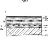
- Fig. 2 is a partial A-A' cross-sectional view of the spectacle lens 1.
- the spectacle lens 1 includes a spectacle lens substrate 11 (hereinafter, also simply referred to as "lens substrate"), and includes a hard coat layer 13, a metal layer 15, an antireflection layer 17, and a water-repellent layer 19 in this order on a first principal surface of the lens substrate 11.
- a processed pattern 15b containing metal is formed.
- apertures 15a having shapes of a plurality of minute dots are formed.
- the dots D of the spectacle lens 1 are formed by the apertures 15a.
- the apertures 15a are arranged isotropically and evenly.
- the apertures 15a are gathered to form a watermark such as a logo. In this way, when the apertures 15a having shapes of a plurality of minute dots are arranged isotropically with an even pitch, uncomfortable feeling on a field of view of a wearer of the spectacle lens 1 can be alleviated while a viewable watermark is formed.
- Examples of the metal that is the material of the processed pattern 15b include at least one kind of metal selected from Cr, Ta, Nb, Ti, Zr, Au, Ag, and Al, and from the viewpoint of adhesive property, Cr is preferable. Incidentally, when metal is used as the material of the processed pattern 15b, an antistatic effect is also exhibited.
- the lens substrate 11 includes a first principal surface 111, a second principal surface 112, and a cut end surface 113.
- the material of the lens substrate 11 may be either plastic or inorganic glass.
- the material of the substrate include a polyurethane-based material such as a polythiourethane resin or a polyurethane resin, an epithio-based material such as a polysulfide resin, a polycarbonate-based material, and a diethylene glycol bis allyl carbonate-based material.
- Colorless ones are usually used as the lens substrate 11, but it is also possible to use colored ones as long as the transparency is not impaired.
- the refractive index of the lens substrate 11 is, for example, 1.50 or more and 1.74 or less.
- the lens substrate 11 may be either a finished lens or a semi-finished lens.
- the surface shape of the lens substrate 11 is not particularly limited, and any shapes such as a flat shape, a convex shape, and a concave shape may be employed.
- the spectacle lens of the present disclosure may be any of a single focus lens, a multifocal lens, a progressive power lens, and the like.
- a near portion region (near portion) and a corridor region (intermediate region) are included in the aforementioned lower region and a distance portion region (distance portion) is included in the upper region.
- the hard coat layer 13 is obtained by, for example, curing a curable composition containing inorganic oxide particles and a silicon compound.
- the composition of the hard coat layer 13 is selected depending on the material of the lens substrate 11.
- the refractive index (nD) of the hard coat layer 13 is, for example, 1.50 or more and 1.74 or less.
- the antireflection layer 17 has a multi-layer structure formed by alternately or continuously laminating films each having a different refractive index, and is a film to prevent light refection by interference.
- Examples of such an antireflection layer 17 include one which has a multi-layer structure formed by laminating a plurality of low refractive index layers 17L and high refractive index layers 17H.
- the refractive index of the low refractive index layer 17L is, for example, 1.35 to 1.80 in a wavelength of 500 to 550 nm.
- the refractive index of the high refractive index layer 17H is, for example, 1.90 to 2.60 in a wavelength of 500 to 550 nm.
- the low refractive index layer 17L is formed by, for example, silica dioxide (SiO 2 ) which has a refractive index of about 1.43 to 1.47.
- the high refractive index layer 17H is formed by a material having a higher refractive index than that of the low refractive index layer 17L, and for example, such a material is composed of, at an appropriate ratio, metal oxides such as niobium oxide (Nb 2 O 5 ), tantalum oxide (Ta 2 O 5 ), titanium oxide (TiO 2 ), zirconium oxide (ZrO 2 ), yttrium oxide (Y 2 O 3 ), and aluminum oxide (Al 2 O 3 ).
- the water-repellent layer 19 contains, for example, a fluorine-substituted alkyl group-containing organosilicon compound. This water-repellent layer 19 has a thickness which is set such that antireflection function is exhibited in combination with the antireflection layer 17.
- FIG. 3 is a flowchart illustrating a method for producing the spectacle lens 1.
- Figs. 4 to 6 are process diagrams illustrating the method for producing the spectacle lens 1 according to the embodiment having the aforementioned configuration.
- the hard coat layer 13 is formed on the lens substrate 11.
- the hard coat layer 13 is formed, for example, by forming a film by a dipping method using a solution, which is obtained by dissolving a curable composition containing inorganic oxide particles and a silicon compound, and curing the film.
- a resist pattern 21 containing a water-soluble polymer is formed on the spectacle lens 1.
- the resist pattern 21 is formed using an inkjet apparatus 5 by an inkjet recording method.
- the process can be simplified and a minute processed pattern can be formed.
- the resist pattern causes a region in which the hard coat layer or the water-insoluble layer of the lens substrate is formed to be exposed.
- ultraviolet (UV) irradiation is performed on the resist pattern 21 to cure an ink forming the resist pattern 21.
- the curing time of curing by ultraviolet irradiation is shorter than that of curing by heating.
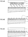
- Figs. 4A to 4C are process diagrams of the resist pattern forming step (S2).
- S2 a plurality of droplets d are discharged from inkjet nozzles 51.
- the discharged droplets are bonded to other droplets d on the surface of the spectacle lens 1 to form one dot portion 21a.
- the dot portion 21a in which the plurality of droplets d are gathered in this way is arranged to form a resist pattern.
- the resist pattern 21 is cured by subjecting the resist pattern 21 to irradiation with light such as ultraviolet (UV) by using an ultraviolet irradiation apparatus 6.
- UV ultraviolet
- Marks such as characters and figures are formed by the aggregate of the dot portions 21a on the spectacle lens 1 formed by the resist pattern 21.
- the formation surface preferably has a high hydrophobicity, and for example, it is preferable to form the resist pattern on a surface not subjected to a hydrophilic treatment such as a plasma treatment, an ion irradiation treatment, a corona discharge treatment, or an alkali treatment.
- a hydrophilic treatment such as a plasma treatment, an ion irradiation treatment, a corona discharge treatment, or an alkali treatment.
- the ink used in the inkjet recording method contains, from the viewpoint of obtaining excellent removing property by the water-based solvent in a removing step (S4) to be described later and from the viewpoint of discharge stability of the ink, preferably a water-soluble polymer, and contains, from the viewpoint of obtaining excellent removing property by the water-based solvent and curability, more preferably a water-soluble polymer and a (meth)acrylic monomer.
- water-soluble polymer examples include polyvinylpyrrolidone, polyvinyl alcohol, and polyacrylic acid. Of these, from the viewpoint of obtaining excellent removing property by the water-based solvent, polyvinylpyrrolidone is preferable.
- the weight average molecular weight of the water-soluble polymer is, from the viewpoint of obtaining excellent removing property by the water-based solvent, preferably 100 or more, more preferably 300 or more, further preferably 400 or more, further preferably 1, 000 or more, and further preferably 5, 000 or more, and is preferably 100, 000 or less. From the viewpoint of discharge stability of the ink in the inkjet recording method, the weight average molecular weight thereof is more preferably 30,000 or less and further preferably 15,000 or less.
- the content of the water-soluble polymer in the ink is, from the viewpoint of obtaining excellent removing property by the water-based solvent, preferably 1% by mass or more, more preferably 2% by mass or more, and further preferably 3% by mass or more, and is preferably 30% by mass or less, more preferably 20% by mass or less, further preferably 10% by mass or less, and further preferably 8% by mass or less. From the viewpoint of obtaining excellent curability, the content thereof is further preferably 5% by mass or less and further preferably 4% by mass or less.
- Examples of the (meth)acrylic monomer include monofunctional (meth)acrylate and multifunctional (meth)acrylate. Of these, from the viewpoint of curability after forming the resist pattern, a combination of monofunctional (meth)acrylate and multifunctional (meth)acrylate is preferable.
- the (meth) acrylate means at least one kind selected from acrylate and methacrylate.
- Examples of the monofunctional (meth)acrylate include polyethylene glycol mono(meth)acrylate and alkoxy polyethylene glycol mono(meth)acrylate.
- the number of carbon atoms in the alkoxy group of alkoxy polyethylene glycol mono(meth)acrylate is preferably 1 to 4, more preferably 1 to 3, and further preferably 1 or 2.
- Examples of the polyethylene glycol mono(meth)acrylate include diethylene glycol mono(meth)acrylate and triethylene glycol mono(meth)acrylate.
- Examples of the alkoxy polyethylene glycol mono(meth)acrylate include methoxy polyethylene glycol mono(meth)acrylate and ethoxy polyethylene glycol mono(meth)acrylate.
- Examples of the methoxy polyethylene glycol mono(meth)acrylate include methoxy diethylene glycol mono(mono)acrylate and methoxy triethylene glycol mono (mono) acrylate.
- Examples of the ethoxy polyethylene glycol mono(mono)acrylate include ethoxy diethylene glycol monoacrylate and ethoxy triethylene glycol monoacrylate.
- alkoxy polyethylene glycol mono(meth)acrylate is preferable, methoxy polyethylene glycol monoacrylate is more preferable, and methoxy triethylene glycol monoacrylate is further preferable.
- the multifunctional (meth)acrylate is preferably difunctional (meth)acrylate.
- the difunctional (meth)acrylate include polyethylene glycol di(meth)acrylates. Among them, from the viewpoint of curability after forming the resist pattern and from the viewpoint of discharge stability of the ink in the inkjet recording method, polyethylene glycol diacrylate is preferable.
- the average addition mole number at the polyethylene glycol site of the polyethylene glycol diacrylate is preferably 3 or more, more preferably 6 or more, and further preferably 9 or more, and is preferably 30 or less, more preferably 25 or less, and further preferably 18 or less.
- the content of (meth)acrylate in the ink is preferably 10% by mass or more, more preferably 20% by mass or more, and further preferably 30% by mass or more, and is preferably 70% by mass or less, more preferably 60% by mass or less, and further preferably 50% by mass or less.
- the content of monofunctional (meth)acrylate in the ink is preferably 10% by mass or more, more preferably 20% by mass or more, and further preferably 30% by mass or more, and is preferably 70% by mass or less, more preferably 60% by mass or less, and further preferably 50% by mass or less.
- the content of multifunctional (meth) acrylate in the ink is preferably 1% by mass or more, more preferably 3% by mass or more, and further preferably 5% by mass or more, and is preferably 30% by mass or less, more preferably 20% by mass or less, and further preferably 10% by mass or less.
- the mass ratio of multifunctional (meth)acrylate/monofunctional (meth)acrylate is, from the viewpoint of curability, preferably 5/95 or more, more preferably 8/92 or more, and further preferably 10/90 or more, and is preferably 40/60 or less, more preferably 30/70 or less, and further preferably 20/80 or less.
- a photopolymerization initiator As a photopolymerization initiator, a photopolymerization initiator having two or more hydroxyl groups is preferable.
- photopolymerization initiator for example, 1-[4-(2-hydroxyethoxy)-phenyl]-2-hydroxy-2-methyl-1-propane -1-one is mentioned.
- the content of the photopolymerization initiator in the ink is, from the viewpoint of enhancing curability, preferably 1% by mass or more, more preferably 3% by mass or more, and further preferably 5% by mass or more, and is preferably 30% by mass or less, more preferably 20% by mass or less, and further preferably 10% by mass or less.
- the content of the photopolymerization initiator is, from the viewpoint of curability, preferably 5 parts by mass or more, more preferably 8 parts by mass or more, and further preferably 10 parts by mass or more, and is preferably 40 parts by mass or less, more preferably 30 parts by mass or less, and further preferably 20 parts by mass or less with respect to the total amount 100 parts by mass of (meth)acrylate.
- the ink preferably contains a high-boiling-point solvent.
- the boiling point of the high-boiling-point solvent is preferably 150°C or higher, more preferably 160°C or higher, further preferably 170°C or higher, and further preferably 180°C or higher, and is preferably 350°C or lower, more preferably 330°C or lower, and further preferably 300°C or lower.
- the high-boiling-point solvent examples include an oxyethylene or oxypropylene addition polymer such as diethylene glycol, triethylene glycol, tetraethylene glycol, or tripropylene glycol; a diol such as propylene glycol; a triol such as glycerin; thiodiglycol; a lower alkyl glycol ether such as triethylene glycol monoethyl ether or triethylene glycol monobutyl ether; and a lower dialkyl glycol ether such as triethylene glycol diethyl ether, tetraethylene glycol dimethyl ether, or tetraethylene glycol diethyl ether. They can be used either singly or in combination of two or more kinds thereof. Among them, propylene glycol is preferable.
- the content of the high-boiling-point solvent in the ink is preferably 5% by mass or more, more preferably 10% by mass or more, and further preferably 15% by mass or more, and is preferably 40% by mass or less, more preferably 30% by mass or less, and further preferably 20% by mass or less.
- the ink preferably contains water.
- Examples of the water include tap water, pure water, and ion-exchange water.
- the content of the water in the ink is preferably 10% by mass or more, more preferably 20% by mass or more, and further preferably 30% by mass or more, and is preferably 80% by mass or less, more preferably 70% by mass or less, and further preferably 60% by mass or less.
- the viscosity of the ink is, from the viewpoint of arranging the ink by the inkjet recording method, preferably 1 mPa ⁇ s or more, more preferably 5 mPa ⁇ s or more, and further preferably 8 mPa ⁇ s or more, and is preferably 40 mPa ⁇ s or less, more preferably 30 mPa ⁇ s or less, further preferably 20 mPa ⁇ s or less, and further preferably 15 mPa ⁇ s or less.
- the pH of the ink is preferably 3.0 or more, more preferably 3.5 or more, and further preferably 4.0 or more, and is preferably 12 or less, more preferably 11 or less, and further preferably 10 or less.
- the contact angle of the ink with respect to a resist pattern formation surface is, from the viewpoint that the dot shape of the resist pattern is formed to be closer to a true circle, preferably 25° or more, more preferably 30° or more, and further preferably 45° or more, and is preferably 65° or less, more preferably 60° or less, further preferably 55° or less, and further preferably 53° or less.
- the contact angle is a value measured by a sessile drop method of JIS R 3257 : 1990.
- the "resist pattern formation surface” means a surface on which the resist pattern in which the ink is arranged is formed.
- the inkjet recording method used herein is not particularly limited in the type and the method, but may either be a continuation type or an on-demand type; and if the inkjet recording method is an on-demand type, it may either be a piezoelectric system or a thermal system.
- Examples of printing conditions include a moving speed of the lens substrate with respect to a printing head, a resolution in a moving direction, a resolution in a width direction perpendicular to the moving direction, a size of an ink droplet, a drop frequency of an ink droplet, and the number of ink droplets dropped to the same point of impact. Since these printing conditions are correlated to each other, the resist pattern 21 is formed by suitably adjusting the printing conditions.
- the resist pattern 21 has the dot portions 21a corresponding to the apertures 15a to be formed on the optical component.
- the resist pattern 21 has a plurality of dot portions 21a arranged isotropically and evenly.
- the plurality of dot portions 21a are arranged, for example, in a lattice shape.
- the plurality of dot portions 21a may be formed on the lens substrate or the entire surface of one principal surface of the lens substrate having the hard coat layer.
- An interval AD between the center of the dot portion 21a and the center of the adjacent dot portion 21a is, for example, 0.1 mm or more, preferably 0.2 mm or more, and more preferably 0.3 mm or more, and is, for example, 5.0 mm or less, preferably 3.0 mm or less, and more preferably 1.0 mm or less.
- a diameter DD of the dot is, for example, 0.01 mm or more, more preferably 0.05 mm or more, and further preferably 0.1 mm or more, and is, for example, 5.0 mm or less, preferably 2.0 mm or less, more preferably 1.0 mm or less, and further preferably 0.5 mm or less.
- the interval AD/the diameter DD is preferably more than 1.0, more preferably 1.1 or more, and further preferably 1.2 or more, and is preferably 2.0 or less, more preferably 1.8 or less, and further preferably 1.5 or less.
- the dot density in the inkjet recording method is, from the viewpoint of improving resist pattern formability, preferably 300 dpi (dots per inch) or more, more preferably 400 dpi or more, and further preferably 500 dpi or more, and is preferably 1,000 dpi or less, more preferably 900 dpi or less, and further preferably 800 dpi or less.
- the ink discharge amount per dot is, from the viewpoint of enhancing curability of the formed dots and improving resist pattern formability, preferably 600 pl (picolitre) or more, more preferably 1,000 pl or more, and further preferably 2,000 pl or more, and is preferably 600 pl or less, more preferably 5,000 pl or less, and further preferably 4,000 pl or less.
- a water-insoluble layer is formed on the spectacle lens 1 having the resist pattern 21 formed thereon.
- Fig. 5 is a process diagram of the water-insoluble layer forming step (S3). As illustrated in Fig. 5 , for example, in S3, the metal layer 15 is deposited as the water-insoluble layer by a vapor deposition apparatus 7.
- a removing step (S4) the water-insoluble layer formed on the resist pattern is peeled off by removing the resist pattern 21 with an water-based solvent.
- Fig. 6 is a cross-sectional view of the spectacle lens 1 after the removing step (S4).
- the resist pattern 21 containing a water-soluble polymer is removed with the water-based solvent to peel off the metal layer formed on the resist pattern 21, thereby obtaining the spectacle lens 1 including the metal layer 15 having the apertures 15a formed thereon. It is possible to prevent the surface erosion of the spectacle lens like the surface erosion caused when an organic solvent is used for removing the resist pattern, and it is possible to obtain a spectacle lens having a processed pattern formed thereon while the surface erosion thereof is suppressed when the water-based solvent is used.
- the water-based solvent means a solvent containing 60% by mass or more of water.
- water is preferable.
- examples of a solvent, which may be contained in the water-based solvent, other than water include an alcohol-based solvent such as ethanol, methanol, or propanol, and a ketone-based solvent such as acetone or methyl ethyl ketone.
- the content of the water in the water-based solvent is preferably 80% by mass or more, more preferably 90% by mass or more, further preferably 95% by mass or more, and further preferably 100% by mass.
- the removing of the metal layer 15 formed on the resist pattern 21 is performed by immersing the metal layer in the water-based solvent.
- the temperature of the water-based solvent is preferably 15°C or higher, and more preferably 20°C or higher, and is preferably 70°C or lower, more preferably 60°C or lower, and further preferably 55°C or lower.
- Ultrasonic irradiation may be performed at the time of immersion.
- the frequency of the ultrasonic wave is, for example, 29 kHz or more and 50 kHz or less.
- the metal layer 15 on the dot portion 21a of the resist pattern is peeled off by the removing step to form the aperture 15a, which is formed at the same position as that of the dot portion 21a and has the same shape as that of the dot portion 21a, on the metal layer 15, thereby forming the processed pattern 15b.
- a functional layer is formed after the removing step.
- the functional layer for example, the antireflection layer 17 and the water-repellent layer 19 are formed.
- the antireflection layer 17 is formed by alternately or continuously laminating the low refractive index layer 17L and the high refractive index layer 17H.
- the antireflection layer 17 is formed such that each layer is formed in order from the low refractive index layer 17L at the lower layer side to have each composition and each thickness. Ion assisted deposition may be employed for the film formation.
- water-repellent layer 19 may be further formed on the outermost surface.
- the resist pattern 21 is formed by a specific ink.
- the water-insoluble layer forming step the water-insoluble layer 15 is formed on the resist pattern 21.
- the resist pattern 21 is removed with an water-based solvent. According to the above steps, the metal layer 15 formed on the resist pattern 21 is peeled off to form the processed pattern 15b and the aperture 15a.
- compositions described in Examples are adjusted to be the compositions described in the detailed description of the invention, the embodiments of the disclosure can be carried out over the entire composition range claimed, similarly to Examples.
- Measurement methods and evaluation methods for various physical properties were performed by the following methods.
- the pH of the ink was measured using a pH meter (manufactured by HORIBA, Ltd., trade name "D-51") under the condition of a temperature of 25°C by a glass electrode method.
- the viscosity of the ink was measured using a tuning fork vibration viscometer (manufactured by A&D Company, Limited, trade name "SV-10") under the condition of a temperature of 25°C according to JIS Z 8803:2011.
- a hard coat layer formed by a hard coat liquid "HC60S” (manufactured by HOYA CORPORATION) was provided on a spectacle lens substrate produced by a monomer for a spectacle lens "MR 8" (manufactured by Mitsui Chemicals, Inc.), an ink was dropped on the lens substrate, and then the contact angle was measured by the method described in "6. Sessile Drop Method" of JIS R 3257:1990.
- polyethylene glycol diacrylate (average addition mole number of 14, CAS No. 26570-48-9 ), methoxytriethylene glycol acrylate ( CAS No. 48067-72-7 ), and water were added thereto and stirred. Thereafter, propylene glycol was added thereto and further stirred. Further, 1% by mass of NaOH water-based solution was added thereto to adjust the pH. Thereafter, a photoinitiator "IRGACURE 2959" (manufactured by BASF) was further added thereto and stirred, 20% by mass of polyvinylpyrrolidone water-based solution (weight average molecular weight of 10,000, CAS No.
- a resist pattern having lattice dots with a dot interval of 0.432 nm and a dot diameter of 0.323 nm was formed using the obtained ink by an inkjet apparatus equipped with a nozzle "KJ4A" (manufactured by KYOCERA Corporation) at a dot density of 9600 ⁇ 600 dpi and a print width of 108 mm on a spectacle lens substrate produced by a monomer for a spectacle lens "MR 8" (manufactured by Mitsui Chemicals, Inc.) on which a hard coat layer formed by a hard coat liquid "HC60S” (manufactured by HOYA CORPORATION) is formed (the resist pattern was entirely formed on the hard coat layer at one principal surface side of the lens substrate) .
- the droplet amount per dot was set to 2400 pl.
- the resist pattern on the spectacle lens substrate was cured by irradiation at a wavelength of 365 nm and an irradiation amount of 900 mJ/cm 2 with a linear UV-LED "H-16LH4-V1-SM2" (manufactured by HOYA CANDEO OPTRONICS CORPORATION). It was possible to produce the resist pattern to have a circular dot without lattice defect.
- a single chromium layer was deposited using argon as assist gas by ion assisted deposition.
- the spectacle lens substrate on which the single chromium layer was deposited was immersed in water at 20°C for 5 minutes or immersed in water at 20°C and subjected to irradiation with ultrasonic wave for 5 minutes to thereby obtain a spectacle lens on which a processed pattern formed by the single chromium layer and having apertures was formed.
- the erosion on the spectacle lens surface was not observed.
- the evaluation of removing property was performed by a ratio (%) of the number of dots removed which configure the resist pattern.
- removing property "absence of US” means the evaluation result without ultrasonic irradiation and removing property "presence of US” means the evaluation result with ultrasonic irradiation.
- Ink 51 was obtained by the same method as in Example 1, except that a polyvinylpyrrolidone water-based solution was not added and the composition was changed to the composition presented in Table 1, and the resist pattern formation, the processed pattern formation, and evaluations thereof were performed.
- Example/Comparative Example Example 1 Example 2
- Example 3 Example 4
- Example 5 Example 6 Reference Example 1 Production
- Ink 1 2 3 4 5 6 51 Blending amount (parts by mass) Water-soluble polymer PVP 1 2 3.5 5 5 10 0
- Acrylic monomer PEGDA 5 5 5 5 5 7.5 1 5 MEA 30 30 35 12.5 12.5 20 35 High-boiling-point solvent PG 20 15 18 40 20 30 22 Water 39 43 33.5 32.5 50 34
- Physical property Viscosity (mPa ⁇ s) 9.5 8.6 14.5 13.8 13.2 14.8 13.9
- the method for producing an optical component having a pattern formed thereon includes, as illustrated in Figs. 1 to 4 , the resist pattern forming step S2 of forming the resist pattern 21 containing a water-soluble polymer on the lens substrate 11, the water-insoluble layer forming step S3 of forming the water-insoluble layer (for example, the metal layer 15) on the lens substrate having the resist pattern 21 formed thereon, and the removing step S4 of removing the water-insoluble layer formed on the resist pattern 21 by removing the resist pattern 21 with an water-based solvent to form the processed pattern 15b.
- An optical component having the above-described pattern formed thereon can be obtained by using the aforementioned resist pattern 21 containing a water-soluble polymer and removing the resist pattern 21 with an water-based solvent in the removing step S4.
- the method for producing an optical component having a pattern formed thereon forms the resist pattern by curing the ink containing a water-soluble polymer in the resist pattern forming step S2, in which the ink further contains a water-soluble polymer and a (meth)acrylic monomer.
- the method for producing an optical component having a pattern formed thereon includes the resist pattern forming step S2 of forming the resist pattern 21 on the lens substrate, the water-insoluble layer forming step S3 of forming the water-insoluble layer (for example, the metal layer 15) on the lens substrate having the resist pattern 21 formed thereon, and the removing step S4 of removing the water-insoluble layer formed on the resist pattern 21 by removing the resist pattern 21 with an water-based solvent to form the processed pattern 15b.
- the method for producing an optical component having a pattern formed thereon forms the resist pattern by curing the ink in the resist pattern forming step S2, in which a contact angle of the ink with respect to the resist pattern formation surface is preferably 25° or more and 65° or less.
- the dot shape of the resist pattern can be formed to be close to a true circle.
Landscapes
- Physics & Mathematics (AREA)
- General Physics & Mathematics (AREA)
- Engineering & Computer Science (AREA)
- Ophthalmology & Optometry (AREA)
- Health & Medical Sciences (AREA)
- Spectroscopy & Molecular Physics (AREA)
- Manufacturing & Machinery (AREA)
- Mechanical Engineering (AREA)
- Architecture (AREA)
- Structural Engineering (AREA)
- Plasma & Fusion (AREA)
- Chemical & Material Sciences (AREA)
- Chemical Kinetics & Catalysis (AREA)
- General Health & Medical Sciences (AREA)
- Optics & Photonics (AREA)
- Photosensitive Polymer And Photoresist Processing (AREA)
- Eyeglasses (AREA)
- Surface Treatment Of Optical Elements (AREA)
Abstract
Description
- The present disclosure relates to a method for producing an optical component having a processed pattern formed thereon.
- A spectacle lens has various layers that coat the surface of a lens substrate. Examples of the various layers include a hard coat layer for preventing the lens substrate from being scratched, an antireflection layer for preventing light from being reflected by a lens surface, and a water-repellent layer for preventing water spotting on the lens. In addition, recently, a coating method for forming a predetermined pattern on an optical component has been proposed (for example,
JP 2008-55253 A - According to the method for forming a processed pattern of
JP 2008-55253 A - In this regard, the present disclosure is intended to provide a method for producing an optical component, the method capable of forming a processed pattern on the optical component by using an water-based solvent in a removing step.
- A method for producing an optical component having a processed pattern formed thereon according to an embodiment of the present disclosure includes:
- a resist pattern forming step of forming a resist pattern containing a water-soluble polymer on a lens substrate;
- a water-insoluble layer forming step of forming a water-insoluble layer on the lens substrate on which the resist pattern is formed; and
- a removing step of removing the water-insoluble layer formed on the resist pattern by removing the resist pattern with an water-based solvent to form a processed pattern.
- An optical component having a processed pattern formed thereon can be obtained by using the formation of the aforementioned resist pattern containing a water-soluble polymer and removing the resist pattern by an water-based solvent in the removing step.
- A method for producing an optical component having a processed pattern formed thereon according to an embodiment of the present disclosure
forms a resist pattern by curing an ink containing a water-soluble polymer in a resist pattern forming step, in which
the ink further contains a water-soluble polymer and a (meth)acrylic monomer. - With the above-described configuration, even in the case of curing the ink, when the water-soluble polymer is contained in the ink, excellent removing property is exhibited in the removing step.
- According to the method for producing an optical component of an embodiment of the present disclosure, the processed pattern can be formed on the optical component by using the water-based solvent in the removing step.
-
-
Fig. 1 is a plan view of a spectacle lens; -
Fig. 2 is a partial A-A' cross-sectional view of the spectacle lens; -
Fig. 3 is a flowchart illustrating a method for producing the spectacle lens; -
Figs. 4A to 4C are process diagrams of a resist pattern forming step; -
Fig. 5 is a schematic diagram of a water-insoluble layer forming step; and -
Fig. 6 is a partial cross-sectional view of thespectacle lens 1 after a removing step. - The definitions of terms in the present specification will be described below.
- The term "resist pattern" means a coating material having an exposed portion in a region in which a processed pattern is formed. The resist pattern is also referred to as a mask pattern.
- The term "water-soluble" means a property of 1 g or more of the compound being dissolved in 100 g of water at 25°C, and the term "water-insoluble" means a property of less than 1 g of the compound being dissolved in 100 g of water at 25°C.
- The term "processed pattern" means a water-insoluble layer portion remaining after the resist pattern is removed.
- Hereinafter, an embodiment and an example of the present disclosure will be described. The same and corresponding portions are denoted by the same reference numerals, and redundant description will not be repeated. In the embodiment and the example described below, when the number, an amount, or the like is mentioned, the scope of the present disclosure is not necessarily limited to that number, that amount, or the like, unless otherwise specified. In the embodiment described below, each component of a configuration is not necessarily essential to the embodiment and the example of the present disclosure unless otherwise specified.
-
Fig. 1 is a plan view of aspectacle lens 1. The configuration of thespectacle lens 1 will be described with reference toFig. 1 . Moreover, description will be made by using, as an example, a case where a metal layer to be described later is used as a water-insoluble layer. - In the
spectacle lens 1, a plurality of minute dots D are arranged isotropically and evenly and watermarks M are formed by the dots D. In this embodiment, the case of forming the watermarks M is exemplified, but the plurality of minute dots may be formed on the entire surface. - The expression "arranged isotropically and evenly" means that the dots are arranged in one direction with a constant interval. The term "constant interval" means arrangement in which a distance between the dot center of the dot and the dot center of the adjacent dot is, for example, within ±40% in terms of average value.
-
Fig. 2 is a partial A-A' cross-sectional view of thespectacle lens 1. As illustrated inFig. 2 , thespectacle lens 1 includes a spectacle lens substrate 11 (hereinafter, also simply referred to as "lens substrate"), and includes ahard coat layer 13, ametal layer 15, anantireflection layer 17, and a water-repellent layer 19 in this order on a first principal surface of thelens substrate 11. - In the
spectacle lens 1, a processedpattern 15b containing metal is formed. - In the processed
pattern 15b,apertures 15a having shapes of a plurality of minute dots are formed. The dots D of thespectacle lens 1 are formed by theapertures 15a. Theapertures 15a are arranged isotropically and evenly. Theapertures 15a are gathered to form a watermark such as a logo. In this way, when theapertures 15a having shapes of a plurality of minute dots are arranged isotropically with an even pitch, uncomfortable feeling on a field of view of a wearer of thespectacle lens 1 can be alleviated while a viewable watermark is formed. - Examples of the metal that is the material of the processed
pattern 15b include at least one kind of metal selected from Cr, Ta, Nb, Ti, Zr, Au, Ag, and Al, and from the viewpoint of adhesive property, Cr is preferable. Incidentally, when metal is used as the material of the processedpattern 15b, an antistatic effect is also exhibited. - Further, the
lens substrate 11 will be described with reference toFig. 2 . Thelens substrate 11 includes a firstprincipal surface 111, a secondprincipal surface 112, and a cut end surface 113. - The material of the
lens substrate 11 may be either plastic or inorganic glass. Examples of the material of the substrate include a polyurethane-based material such as a polythiourethane resin or a polyurethane resin, an epithio-based material such as a polysulfide resin, a polycarbonate-based material, and a diethylene glycol bis allyl carbonate-based material. - Colorless ones are usually used as the
lens substrate 11, but it is also possible to use colored ones as long as the transparency is not impaired. - The refractive index of the
lens substrate 11 is, for example, 1.50 or more and 1.74 or less. - The
lens substrate 11 may be either a finished lens or a semi-finished lens. - The surface shape of the
lens substrate 11 is not particularly limited, and any shapes such as a flat shape, a convex shape, and a concave shape may be employed. - The spectacle lens of the present disclosure may be any of a single focus lens, a multifocal lens, a progressive power lens, and the like. Regarding the progressive power lens, usually, a near portion region (near portion) and a corridor region (intermediate region) are included in the aforementioned lower region and a distance portion region (distance portion) is included in the upper region.
- The
hard coat layer 13 is obtained by, for example, curing a curable composition containing inorganic oxide particles and a silicon compound. The composition of thehard coat layer 13 is selected depending on the material of thelens substrate 11. Incidentally, the refractive index (nD) of thehard coat layer 13 is, for example, 1.50 or more and 1.74 or less. - The
antireflection layer 17 has a multi-layer structure formed by alternately or continuously laminating films each having a different refractive index, and is a film to prevent light refection by interference. Examples of such anantireflection layer 17 include one which has a multi-layer structure formed by laminating a plurality of low refractive index layers 17L and high refractive index layers 17H. The refractive index of the lowrefractive index layer 17L is, for example, 1.35 to 1.80 in a wavelength of 500 to 550 nm. The refractive index of the highrefractive index layer 17H is, for example, 1.90 to 2.60 in a wavelength of 500 to 550 nm. - The low
refractive index layer 17L is formed by, for example, silica dioxide (SiO2) which has a refractive index of about 1.43 to 1.47. In addition, the highrefractive index layer 17H is formed by a material having a higher refractive index than that of the lowrefractive index layer 17L, and for example, such a material is composed of, at an appropriate ratio, metal oxides such as niobium oxide (Nb2O5), tantalum oxide (Ta2O5), titanium oxide (TiO2), zirconium oxide (ZrO2), yttrium oxide (Y2O3), and aluminum oxide (Al2O3). - The water-
repellent layer 19 contains, for example, a fluorine-substituted alkyl group-containing organosilicon compound. This water-repellent layer 19 has a thickness which is set such that antireflection function is exhibited in combination with theantireflection layer 17. - Next, a method for producing an optical component according to this embodiment will be described with reference to
Fig. 3. Fig. 3 is a flowchart illustrating a method for producing thespectacle lens 1.Figs. 4 to 6 are process diagrams illustrating the method for producing thespectacle lens 1 according to the embodiment having the aforementioned configuration. - In a hard coat layer forming step (S1), the
hard coat layer 13 is formed on thelens substrate 11. Thehard coat layer 13 is formed, for example, by forming a film by a dipping method using a solution, which is obtained by dissolving a curable composition containing inorganic oxide particles and a silicon compound, and curing the film. - In a resist pattern forming step (S2), a resist
pattern 21 containing a water-soluble polymer is formed on thespectacle lens 1. For example, the resistpattern 21 is formed using aninkjet apparatus 5 by an inkjet recording method. When the resist pattern is formed using the inkjet recording method, the process can be simplified and a minute processed pattern can be formed. The resist pattern causes a region in which the hard coat layer or the water-insoluble layer of the lens substrate is formed to be exposed. After forming the resistpattern 21, ultraviolet (UV) irradiation is performed on the resistpattern 21 to cure an ink forming the resistpattern 21. The curing time of curing by ultraviolet irradiation is shorter than that of curing by heating. -
Figs. 4A to 4C are process diagrams of the resist pattern forming step (S2). As illustrated inFig. 4A , in S2, a plurality of droplets d are discharged frominkjet nozzles 51. Subsequently, as illustrated inFig. 4B , the discharged droplets are bonded to other droplets d on the surface of thespectacle lens 1 to form onedot portion 21a. Thedot portion 21a in which the plurality of droplets d are gathered in this way is arranged to form a resist pattern. Subsequently, as illustrated inFig. 4C , after forming the resist pattern, the resistpattern 21 is cured by subjecting the resistpattern 21 to irradiation with light such as ultraviolet (UV) by using anultraviolet irradiation apparatus 6. - Marks such as characters and figures are formed by the aggregate of the
dot portions 21a on thespectacle lens 1 formed by the resistpattern 21. - From the viewpoint of forming circular dots on the
spectacle lens 1, the formation surface preferably has a high hydrophobicity, and for example, it is preferable to form the resist pattern on a surface not subjected to a hydrophilic treatment such as a plasma treatment, an ion irradiation treatment, a corona discharge treatment, or an alkali treatment. - The ink used in the inkjet recording method contains, from the viewpoint of obtaining excellent removing property by the water-based solvent in a removing step (S4) to be described later and from the viewpoint of discharge stability of the ink, preferably a water-soluble polymer, and contains, from the viewpoint of obtaining excellent removing property by the water-based solvent and curability, more preferably a water-soluble polymer and a (meth)acrylic monomer.
- Examples of the water-soluble polymer include polyvinylpyrrolidone, polyvinyl alcohol, and polyacrylic acid. Of these, from the viewpoint of obtaining excellent removing property by the water-based solvent, polyvinylpyrrolidone is preferable.
- The weight average molecular weight of the water-soluble polymer is, from the viewpoint of obtaining excellent removing property by the water-based solvent, preferably 100 or more, more preferably 300 or more, further preferably 400 or more, further preferably 1, 000 or more, and further preferably 5, 000 or more, and is preferably 100, 000 or less. From the viewpoint of discharge stability of the ink in the inkjet recording method, the weight average molecular weight thereof is more preferably 30,000 or less and further preferably 15,000 or less.
- The content of the water-soluble polymer in the ink is, from the viewpoint of obtaining excellent removing property by the water-based solvent, preferably 1% by mass or more, more preferably 2% by mass or more, and further preferably 3% by mass or more, and is preferably 30% by mass or less, more preferably 20% by mass or less, further preferably 10% by mass or less, and further preferably 8% by mass or less. From the viewpoint of obtaining excellent curability, the content thereof is further preferably 5% by mass or less and further preferably 4% by mass or less.
- Examples of the (meth)acrylic monomer include monofunctional (meth)acrylate and multifunctional (meth)acrylate. Of these, from the viewpoint of curability after forming the resist pattern, a combination of monofunctional (meth)acrylate and multifunctional (meth)acrylate is preferable.
- The (meth) acrylate means at least one kind selected from acrylate and methacrylate.
- Examples of the monofunctional (meth)acrylate include polyethylene glycol mono(meth)acrylate and alkoxy polyethylene glycol mono(meth)acrylate.
- The number of carbon atoms in the alkoxy group of alkoxy polyethylene glycol mono(meth)acrylate is preferably 1 to 4, more preferably 1 to 3, and further preferably 1 or 2.
- Examples of the polyethylene glycol mono(meth)acrylate include diethylene glycol mono(meth)acrylate and triethylene glycol mono(meth)acrylate. Examples of the alkoxy polyethylene glycol mono(meth)acrylate include methoxy polyethylene glycol mono(meth)acrylate and ethoxy polyethylene glycol mono(meth)acrylate. Examples of the methoxy polyethylene glycol mono(meth)acrylate include methoxy diethylene glycol mono(mono)acrylate and methoxy triethylene glycol mono (mono) acrylate. Examples of the ethoxy polyethylene glycol mono(mono)acrylate include ethoxy diethylene glycol monoacrylate and ethoxy triethylene glycol monoacrylate.
- Among these, from the viewpoint of discharge stability of the ink in the inkjet recording method, alkoxy polyethylene glycol mono(meth)acrylate is preferable, methoxy polyethylene glycol monoacrylate is more preferable, and methoxy triethylene glycol monoacrylate is further preferable.
- The multifunctional (meth)acrylate is preferably difunctional (meth)acrylate. Examples of the difunctional (meth)acrylate include polyethylene glycol di(meth)acrylates. Among them, from the viewpoint of curability after forming the resist pattern and from the viewpoint of discharge stability of the ink in the inkjet recording method, polyethylene glycol diacrylate is preferable. The average addition mole number at the polyethylene glycol site of the polyethylene glycol diacrylate is preferably 3 or more, more preferably 6 or more, and further preferably 9 or more, and is preferably 30 or less, more preferably 25 or less, and further preferably 18 or less.
- The content of (meth)acrylate in the ink is preferably 10% by mass or more, more preferably 20% by mass or more, and further preferably 30% by mass or more, and is preferably 70% by mass or less, more preferably 60% by mass or less, and further preferably 50% by mass or less.
- The content of monofunctional (meth)acrylate in the ink is preferably 10% by mass or more, more preferably 20% by mass or more, and further preferably 30% by mass or more, and is preferably 70% by mass or less, more preferably 60% by mass or less, and further preferably 50% by mass or less.
- The content of multifunctional (meth) acrylate in the ink is preferably 1% by mass or more, more preferably 3% by mass or more, and further preferably 5% by mass or more, and is preferably 30% by mass or less, more preferably 20% by mass or less, and further preferably 10% by mass or less.
- The mass ratio of multifunctional (meth)acrylate/monofunctional (meth)acrylate is, from the viewpoint of curability, preferably 5/95 or more, more preferably 8/92 or more, and further preferably 10/90 or more, and is preferably 40/60 or less, more preferably 30/70 or less, and further preferably 20/80 or less.
- As a photopolymerization initiator, a photopolymerization initiator having two or more hydroxyl groups is preferable.
- As the photopolymerization initiator, for example, 1-[4-(2-hydroxyethoxy)-phenyl]-2-hydroxy-2-methyl-1-propane -1-one is mentioned.
- The content of the photopolymerization initiator in the ink is, from the viewpoint of enhancing curability, preferably 1% by mass or more, more preferably 3% by mass or more, and further preferably 5% by mass or more, and is preferably 30% by mass or less, more preferably 20% by mass or less, and further preferably 10% by mass or less.
- The content of the photopolymerization initiator is, from the viewpoint of curability, preferably 5 parts by mass or more, more preferably 8 parts by mass or more, and further preferably 10 parts by mass or more, and is preferably 40 parts by mass or less, more preferably 30 parts by mass or less, and further preferably 20 parts by mass or less with respect to the total amount 100 parts by mass of (meth)acrylate.
- From the viewpoint of improving formability of the resist pattern, the ink preferably contains a high-boiling-point solvent.
- The boiling point of the high-boiling-point solvent is preferably 150°C or higher, more preferably 160°C or higher, further preferably 170°C or higher, and further preferably 180°C or higher, and is preferably 350°C or lower, more preferably 330°C or lower, and further preferably 300°C or lower.
- Examples of the high-boiling-point solvent include an oxyethylene or oxypropylene addition polymer such as diethylene glycol, triethylene glycol, tetraethylene glycol, or tripropylene glycol; a diol such as propylene glycol; a triol such as glycerin; thiodiglycol; a lower alkyl glycol ether such as triethylene glycol monoethyl ether or triethylene glycol monobutyl ether; and a lower dialkyl glycol ether such as triethylene glycol diethyl ether, tetraethylene glycol dimethyl ether, or tetraethylene glycol diethyl ether. They can be used either singly or in combination of two or more kinds thereof. Among them, propylene glycol is preferable.
- The content of the high-boiling-point solvent in the ink is preferably 5% by mass or more, more preferably 10% by mass or more, and further preferably 15% by mass or more, and is preferably 40% by mass or less, more preferably 30% by mass or less, and further preferably 20% by mass or less.
- From the viewpoint of adjusting a viscosity, the ink preferably contains water.
- Examples of the water include tap water, pure water, and ion-exchange water.
- The content of the water in the ink is preferably 10% by mass or more, more preferably 20% by mass or more, and further preferably 30% by mass or more, and is preferably 80% by mass or less, more preferably 70% by mass or less, and further preferably 60% by mass or less.
- The viscosity of the ink is, from the viewpoint of arranging the ink by the inkjet recording method, preferably 1 mPa·s or more, more preferably 5 mPa·s or more, and further preferably 8 mPa·s or more, and is preferably 40 mPa·s or less, more preferably 30 mPa·s or less, further preferably 20 mPa·s or less, and further preferably 15 mPa·s or less.
- The pH of the ink is preferably 3.0 or more, more preferably 3.5 or more, and further preferably 4.0 or more, and is preferably 12 or less, more preferably 11 or less, and further preferably 10 or less.
- The contact angle of the ink with respect to a resist pattern formation surface is, from the viewpoint that the dot shape of the resist pattern is formed to be closer to a true circle, preferably 25° or more, more preferably 30° or more, and further preferably 45° or more, and is preferably 65° or less, more preferably 60° or less, further preferably 55° or less, and further preferably 53° or less. The contact angle is a value measured by a sessile drop method of JIS R 3257 : 1990. Herein, the "resist pattern formation surface" means a surface on which the resist pattern in which the ink is arranged is formed.
- The inkjet recording method used herein is not particularly limited in the type and the method, but may either be a continuation type or an on-demand type; and if the inkjet recording method is an on-demand type, it may either be a piezoelectric system or a thermal system.
- Examples of printing conditions include a moving speed of the lens substrate with respect to a printing head, a resolution in a moving direction, a resolution in a width direction perpendicular to the moving direction, a size of an ink droplet, a drop frequency of an ink droplet, and the number of ink droplets dropped to the same point of impact. Since these printing conditions are correlated to each other, the resist
pattern 21 is formed by suitably adjusting the printing conditions. - The resist
pattern 21 has thedot portions 21a corresponding to theapertures 15a to be formed on the optical component. The resistpattern 21 has a plurality ofdot portions 21a arranged isotropically and evenly. The plurality ofdot portions 21a are arranged, for example, in a lattice shape. The plurality ofdot portions 21a may be formed on the lens substrate or the entire surface of one principal surface of the lens substrate having the hard coat layer. - An interval AD between the center of the
dot portion 21a and the center of theadjacent dot portion 21a is, for example, 0.1 mm or more, preferably 0.2 mm or more, and more preferably 0.3 mm or more, and is, for example, 5.0 mm or less, preferably 3.0 mm or less, and more preferably 1.0 mm or less. - A diameter DD of the dot is, for example, 0.01 mm or more, more preferably 0.05 mm or more, and further preferably 0.1 mm or more, and is, for example, 5.0 mm or less, preferably 2.0 mm or less, more preferably 1.0 mm or less, and further preferably 0.5 mm or less.
- The interval AD/the diameter DD is preferably more than 1.0, more preferably 1.1 or more, and further preferably 1.2 or more, and is preferably 2.0 or less, more preferably 1.8 or less, and further preferably 1.5 or less.
- The dot density in the inkjet recording method is, from the viewpoint of improving resist pattern formability, preferably 300 dpi (dots per inch) or more, more preferably 400 dpi or more, and further preferably 500 dpi or more, and is preferably 1,000 dpi or less, more preferably 900 dpi or less, and further preferably 800 dpi or less.
- The ink discharge amount per dot is, from the viewpoint of enhancing curability of the formed dots and improving resist pattern formability, preferably 600 pl (picolitre) or more, more preferably 1,000 pl or more, and further preferably 2,000 pl or more, and is preferably 600 pl or less, more preferably 5,000 pl or less, and further preferably 4,000 pl or less.
- In a water-insoluble layer forming step (S3), a water-insoluble layer is formed on the
spectacle lens 1 having the resistpattern 21 formed thereon. -
Fig. 5 is a process diagram of the water-insoluble layer forming step (S3). As illustrated inFig. 5 , for example, in S3, themetal layer 15 is deposited as the water-insoluble layer by avapor deposition apparatus 7. - In a removing step (S4), the water-insoluble layer formed on the resist pattern is peeled off by removing the resist
pattern 21 with an water-based solvent. -
Fig. 6 is a cross-sectional view of thespectacle lens 1 after the removing step (S4). As illustrated inFig. 6 , for example, in the removing step, the resistpattern 21 containing a water-soluble polymer is removed with the water-based solvent to peel off the metal layer formed on the resistpattern 21, thereby obtaining thespectacle lens 1 including themetal layer 15 having theapertures 15a formed thereon. It is possible to prevent the surface erosion of the spectacle lens like the surface erosion caused when an organic solvent is used for removing the resist pattern, and it is possible to obtain a spectacle lens having a processed pattern formed thereon while the surface erosion thereof is suppressed when the water-based solvent is used. - The water-based solvent means a solvent containing 60% by mass or more of water. As the water-based solvent, water is preferable. Examples of a solvent, which may be contained in the water-based solvent, other than water include an alcohol-based solvent such as ethanol, methanol, or propanol, and a ketone-based solvent such as acetone or methyl ethyl ketone.
- The content of the water in the water-based solvent is preferably 80% by mass or more, more preferably 90% by mass or more, further preferably 95% by mass or more, and further preferably 100% by mass.
- The removing of the
metal layer 15 formed on the resistpattern 21 is performed by immersing the metal layer in the water-based solvent. The temperature of the water-based solvent is preferably 15°C or higher, and more preferably 20°C or higher, and is preferably 70°C or lower, more preferably 60°C or lower, and further preferably 55°C or lower. - Ultrasonic irradiation may be performed at the time of immersion. The frequency of the ultrasonic wave is, for example, 29 kHz or more and 50 kHz or less.
- The
metal layer 15 on thedot portion 21a of the resist pattern is peeled off by the removing step to form theaperture 15a, which is formed at the same position as that of thedot portion 21a and has the same shape as that of thedot portion 21a, on themetal layer 15, thereby forming the processedpattern 15b. - In a functional layer forming step (S5), a functional layer is formed after the removing step. As the functional layer, for example, the
antireflection layer 17 and the water-repellent layer 19 are formed. Theantireflection layer 17 is formed by alternately or continuously laminating the lowrefractive index layer 17L and the highrefractive index layer 17H. Theantireflection layer 17 is formed such that each layer is formed in order from the lowrefractive index layer 17L at the lower layer side to have each composition and each thickness. Ion assisted deposition may be employed for the film formation. - In addition, the water-
repellent layer 19 may be further formed on the outermost surface. - As described above, in the resist pattern forming step, the resist
pattern 21 is formed by a specific ink. Next, in the water-insoluble layer forming step, the water-insoluble layer 15 is formed on the resistpattern 21. Subsequently, in the removing step, the resistpattern 21 is removed with an water-based solvent. According to the above steps, themetal layer 15 formed on the resistpattern 21 is peeled off to form the processedpattern 15b and theaperture 15a. - In the present disclosure, regarding the example, the content, and various physical properties of each component described above, matters exemplified in the detailed description of the invention or described as the preferred ranges may be arbitrarily combined.
- Further, if compositions described in Examples are adjusted to be the compositions described in the detailed description of the invention, the embodiments of the disclosure can be carried out over the entire composition range claimed, similarly to Examples.
- Hereinafter, specific examples will be described. However, the scope of the present patent claims is not limited to the following examples.
- Measurement methods and evaluation methods for various physical properties were performed by the following methods.
- The pH of the ink was measured using a pH meter (manufactured by HORIBA, Ltd., trade name "D-51") under the condition of a temperature of 25°C by a glass electrode method.
- The viscosity of the ink was measured using a tuning fork vibration viscometer (manufactured by A&D Company, Limited, trade name "SV-10") under the condition of a temperature of 25°C according to JIS Z 8803:2011.
- A hard coat layer formed by a hard coat liquid "HC60S" (manufactured by HOYA CORPORATION) was provided on a spectacle lens substrate produced by a monomer for a spectacle lens "MR 8" (manufactured by Mitsui Chemicals, Inc.), an ink was dropped on the lens substrate, and then the contact angle was measured by the method described in "6. Sessile Drop Method" of JIS R 3257:1990.
- To a sample bottle, polyethylene glycol diacrylate (average addition mole number of 14, CAS No. 26570-48-9), methoxytriethylene glycol acrylate (CAS No. 48067-72-7), and water were added thereto and stirred. Thereafter, propylene glycol was added thereto and further stirred. Further, 1% by mass of NaOH water-based solution was added thereto to adjust the pH. Thereafter, a photoinitiator "IRGACURE 2959" (manufactured by BASF) was further added thereto and stirred, 20% by mass of polyvinylpyrrolidone water-based solution (weight average molecular weight of 10,000, CAS No. 9003-39-8) was added thereto and stirred, and then the insoluble matter was removed by performing filtering, thereby obtaining
Inks 1 to 6 adjusted topH 7 presented in Table 1 . The viscosity measurement and the contact angle measurement were performed on the obtained inks. The results thereof are presented in Table 1. - A resist pattern having lattice dots with a dot interval of 0.432 nm and a dot diameter of 0.323 nm was formed using the obtained ink by an inkjet apparatus equipped with a nozzle "KJ4A" (manufactured by KYOCERA Corporation) at a dot density of 9600 × 600 dpi and a print width of 108 mm on a spectacle lens substrate produced by a monomer for a spectacle lens "MR 8" (manufactured by Mitsui Chemicals, Inc.) on which a hard coat layer formed by a hard coat liquid "HC60S" (manufactured by HOYA CORPORATION) is formed (the resist pattern was entirely formed on the hard coat layer at one principal surface side of the lens substrate) . Incidentally, the droplet amount per dot was set to 2400 pl. After forming the resist pattern, the resist pattern on the spectacle lens substrate was cured by irradiation at a wavelength of 365 nm and an irradiation amount of 900 mJ/cm2 with a linear UV-LED "H-16LH4-V1-SM2" (manufactured by HOYA CANDEO OPTRONICS CORPORATION). It was possible to produce the resist pattern to have a circular dot without lattice defect.
- The state of dots on the resist pattern after curing was observed and the evaluation of UV curability was performed based on the following criteria.
- A: The resist pattern is completely cured.
- B: The resist pattern is cured while flexibility slightly remains.
- C: The resist pattern is cured while flexibility remains.
- D: The resist pattern is not cured.
- After curing, a single chromium layer was deposited using argon as assist gas by ion assisted deposition.
- The spectacle lens substrate on which the single chromium layer was deposited was immersed in water at 20°C for 5 minutes or immersed in water at 20°C and subjected to irradiation with ultrasonic wave for 5 minutes to thereby obtain a spectacle lens on which a processed pattern formed by the single chromium layer and having apertures was formed. The erosion on the spectacle lens surface was not observed.
- The evaluation of removing property was performed by a ratio (%) of the number of dots removed which configure the resist pattern.
- In the table, removing property "absence of US" means the evaluation result without ultrasonic irradiation and removing property "presence of US" means the evaluation result with ultrasonic irradiation.
-
Ink 51 was obtained by the same method as in Example 1, except that a polyvinylpyrrolidone water-based solution was not added and the composition was changed to the composition presented in Table 1, and the resist pattern formation, the processed pattern formation, and evaluations thereof were performed.[Table 1] Example/Comparative Example Example 1 Example 2 Example 3 Example 4 Example 5 Example 6 Reference Example 1 Production Example 1 2 3 4 5 6 51 Ink 1 2 3 4 5 6 51 Blending amount (parts by mass) Water- soluble polymer PVP 1 2 3.5 5 5 10 0 Acrylic monomer PEGDA 5 5 5 5 7.5 1 5 MEA 30 30 35 12.5 12.5 20 35 High-boiling-point solvent PG 20 15 18 40 20 30 22 Water 39 43 33.5 32.5 50 34 33 Photoinitiator PI-1 5 5 5 5 5 5 5 Physical property Viscosity (mPa·s) 9.5 8.6 14.5 13.8 13.2 14.8 13.9 Contact angle (°) 53 52 50 48 48 45 55 Evaluation UV curability A A A B B C A Removing property (20°C-absence of US) 40% 50% 95% 100% 100% 100% 5% Removing property (20°C-presence of US) 95% 95% 100% 100% 100% 100% 80% - Abbreviated terms in the table mean as follows.
- PVP: polyvinylpyrrolidone (weight average molecular weight of 10,000, CAS No. 9003-39-8)
- PEGDA: polyethylene glycol diacrylate (average addition mole number of 14, CAS No. 26570-48-9)
- MEA: methoxytriethylene glycol acrylate (CAS No. 48067-72-7)
- PG: propylene glycol (boiling point of 188°C)
- PI-1:
1-[4-(2-hydroxyethoxy)-phenyl]-2-hydroxy-2-methyl-1-propane -1-one (CAS No. 106797-53-9) - Finally, the embodiments of the present disclosure will be outlined by use of drawings or the like.
- The method for producing an optical component having a pattern formed thereon according to an embodiment of the present disclosure includes, as illustrated in
Figs. 1 to 4 ,
the resist pattern forming step S2 of forming the resistpattern 21 containing a water-soluble polymer on thelens substrate 11,
the water-insoluble layer forming step S3 of forming the water-insoluble layer (for example, the metal layer 15) on the lens substrate having the resistpattern 21 formed thereon, and
the removing step S4 of removing the water-insoluble layer formed on the resistpattern 21 by removing the resistpattern 21 with an water-based solvent to form the processedpattern 15b. - An optical component having the above-described pattern formed thereon can be obtained by using the aforementioned resist
pattern 21 containing a water-soluble polymer and removing the resistpattern 21 with an water-based solvent in the removing step S4. - The method for producing an optical component having a pattern formed thereon according to an embodiment of the present disclosure
forms the resist pattern by curing the ink containing a water-soluble polymer in the resist pattern forming step S2, in which
the ink further contains a water-soluble polymer and a (meth)acrylic monomer. - With the above-described configuration, even in the case of curing the ink, when the water-soluble polymer is contained in the ink, excellent removing property is exhibited in the removing step.
- The method for producing an optical component having a pattern formed thereon according to an embodiment of the present disclosure includes
the resist pattern forming step S2 of forming the resistpattern 21 on the lens substrate,
the water-insoluble layer forming step S3 of forming the water-insoluble layer (for example, the metal layer 15) on the lens substrate having the resistpattern 21 formed thereon, and
the removing step S4 of removing the water-insoluble layer formed on the resistpattern 21 by removing the resistpattern 21 with an water-based solvent to form the processedpattern 15b. - The method for producing an optical component having a pattern formed thereon according to an embodiment of the present disclosure
forms the resist pattern by curing the ink in the resist pattern forming step S2, in which
a contact angle of the ink with respect to the resist pattern formation surface is preferably 25° or more and 65° or less. - With the above-described configuration, the dot shape of the resist pattern can be formed to be close to a true circle.
- It is to be understood that the aspects of embodiments disclosed herein are not restrictive but illustrative in all respects. The scope of the invention is defined by the appended claims rather than by the foregoing description and is intended to include the meaning equivalent to the scope of the claims and any modifications within the scope.
-
- 1: spectacle lens
- 11: lens substrate
- 13: hard coat layer
- 15: metal layer
- 15a: apertures
- 15b: processed pattern
- 17: antireflection layer
- 17L: low refractive index layers
- 17H: high refractive index layers
- 19: water-repellent layer
- 21: resist pattern
- 21a: dot portion
- D: dots
- M: watermarks
Claims (16)
- A method for producing an optical component having a processed pattern formed thereon, the method comprising:a resist pattern forming step of forming a resist pattern containing a water-soluble polymer on a lens substrate;a water-insoluble layer forming step of forming a water-insoluble layer on the lens substrate on which the resist pattern is formed; anda removing step of removing the water-insoluble layer formed on the resist pattern by removing the resist pattern with an water-based solvent to form a processed pattern.
- The method for producing an optical component according to claim 1, wherein the water-soluble polymer is polyvinylpyrrolidone.
- The method for producing an optical component according to claims 1 or 2, wherein the water-soluble polymer has a weight average molecular weight of 100 or more and 30,000 or less.
- The method for producing an optical component according to any one of claims 1 to 3, wherein in the resist pattern forming step, the resist pattern is formed by curing an ink containing a water-soluble polymer.
- The method for producing an optical component according to claim 4, wherein the ink contains a water-soluble polymer and a (meth)acrylic monomer.
- The method for producing an optical component according to claim 4 or 5, wherein the ink further contains a polymerization initiator, and
in the resist pattern forming step, light irradiation is performed after forming the resist pattern. - The method for producing an optical component according to any one of claims 4 to 6, wherein in the resist pattern forming step, the resist pattern is formed by an inkjet recording method.
- The method for producing an optical component according to any one of claims 4 to 7, wherein the ink further contains a high-boiling-point solvent.
- The method for producing an optical component according to any one of claims 4 to 8, wherein a contact angle of the ink with respect to a resist pattern formation surface is 25° or more and 65° or less.
- The method for producing an optical component according to any one of claims 1 to 9, wherein the water-insoluble layer is a metal layer.
- The method for producing an optical component according to any one of claims 1 to 10, wherein the water-insoluble layer forming step forms the water-insoluble layer by vapor deposition.
- The method for producing an optical component according to any one of claims 1 to 11, wherein the resist pattern has a plurality of dot portions arranged isotropically and evenly.
- The method for producing an optical component according to claim 12, wherein an interval between the center of the dot portion and the center of the adjacent dot portion is 0.1 mm or more and 5.0 mm or less.
- The method for producing an optical component according to any one of claims 1 to 13, further comprising a hard coat layer forming step of forming a hard coat layer on the lens substrate before the resist pattern forming step.
- The method for producing an optical component according to any one of claims 1 to 14, further comprising a functional layer forming step of forming a functional layer after the removing step.
- The method for producing an optical component according to any one of claims 1 to 15, wherein the optical component is a spectacle lens.
Applications Claiming Priority (1)
| Application Number | Priority Date | Filing Date | Title |
|---|---|---|---|
| JP2017077067A JP2018180168A (en) | 2017-04-07 | 2017-04-07 | Method of manufacturing optical member having processing pattern formed thereon |
Publications (2)
| Publication Number | Publication Date |
|---|---|
| EP3385067A2 true EP3385067A2 (en) | 2018-10-10 |
| EP3385067A3 EP3385067A3 (en) | 2019-01-09 |
Family
ID=62067322
Family Applications (1)
| Application Number | Title | Priority Date | Filing Date |
|---|---|---|---|
| EP18164972.4A Withdrawn EP3385067A3 (en) | 2017-04-07 | 2018-03-29 | Method for producing optical component having a processed pattern |
Country Status (3)
| Country | Link |
|---|---|
| US (1) | US20180292754A1 (en) |
| EP (1) | EP3385067A3 (en) |
| JP (1) | JP2018180168A (en) |
Cited By (1)
| Publication number | Priority date | Publication date | Assignee | Title |
|---|---|---|---|---|
| WO2022017918A1 (en) * | 2020-07-23 | 2022-01-27 | Essilor Italia Spa | Method for decorating an ophtalmic article and related ophtalmic article |
Families Citing this family (7)
| Publication number | Priority date | Publication date | Assignee | Title |
|---|---|---|---|---|
| JP7137169B2 (en) * | 2018-12-28 | 2022-09-14 | ホヤ レンズ タイランド リミテッド | spectacle lenses |
| JP7202397B2 (en) * | 2018-12-28 | 2023-01-11 | ホヤ レンズ タイランド リミテッド | OPTICAL MEMBER MANUFACTURING METHOD AND OPTICAL MEMBER |
| JP7479896B2 (en) | 2020-03-30 | 2024-05-09 | ホヤ レンズ タイランド リミテッド | Manufacturing method of lens member |
| JP7479895B2 (en) | 2020-03-30 | 2024-05-09 | ホヤ レンズ タイランド リミテッド | Lens positioning mechanism, lens manufacturing device, and method for manufacturing lens member |
| JP7479894B2 (en) | 2020-03-30 | 2024-05-09 | ホヤ レンズ タイランド リミテッド | Lens positioning mechanism, lens manufacturing device, and method for manufacturing lens member |
| EP4147862A1 (en) * | 2021-09-10 | 2023-03-15 | Carl Zeiss Vision International GmbH | Method for applying a surface pattern on a surface of a spectacle lens substrate and spectacle lens substrate with a surface pattern |
| WO2025073589A1 (en) | 2023-10-05 | 2025-04-10 | Essilor International | Method for manufacturing an optical article and associated optical article |
Family Cites Families (24)
| Publication number | Priority date | Publication date | Assignee | Title |
|---|---|---|---|---|
| JPS5137138B2 (en) * | 1972-01-26 | 1976-10-14 | ||
| GB1423952A (en) * | 1973-06-26 | 1976-02-04 | Oike & Co | Process for preparing a metallized resin film for condenser element |
| US4242378A (en) * | 1979-03-29 | 1980-12-30 | Reiko Co., Ltd. | Method of making a decorated film with a metal layer in the form of a given pattern |
| JPS58223462A (en) * | 1982-06-18 | 1983-12-26 | Fukuda Metal Kogei:Kk | Coating method using masking |
| JPS5978987A (en) * | 1982-10-29 | 1984-05-08 | マルイ工業株式会社 | Formation of pattern on metal coating |
| DE3447357A1 (en) * | 1984-12-24 | 1986-07-03 | Basf Ag, 6700 Ludwigshafen | DRY FILM RESIST AND METHOD FOR PRODUCING RESIST PATTERNS |
| US4895630A (en) * | 1985-08-28 | 1990-01-23 | W. H. Brady Co. | Rapidly removable undercoating for vacuum deposition of patterned layers onto substrates |
| US4714631A (en) * | 1985-08-28 | 1987-12-22 | W. H. Brady Co. | Rapidly removable undercoating for vacuum deposition of patterned layers onto substrates |
| JPH03123675A (en) * | 1989-10-05 | 1991-05-27 | Kojima Press Co Ltd | Method for coating resin molded body |
| JPH07257996A (en) * | 1994-03-17 | 1995-10-09 | Canon Inc | Gold thin film forming method |
| JP2003309346A (en) * | 2002-04-15 | 2003-10-31 | National Institute Of Advanced Industrial & Technology | High-speed printed circuit board creation method |
| US7972472B2 (en) * | 2002-04-24 | 2011-07-05 | Sipix Imaging, Inc. | Process for forming a patterned thin film structure for in-mold decoration |
| KR100733920B1 (en) * | 2004-09-17 | 2007-07-02 | 주식회사 엘지화학 | Ink composition for etching resist, etching resist pattern formation method and fine flow path formation method using same |
| JP2005210113A (en) * | 2005-01-07 | 2005-08-04 | Bridgestone Corp | Method for manufacturing light transmission window material shielding electromagnetic wave |
| JP2006247581A (en) * | 2005-03-11 | 2006-09-21 | Fuji Photo Film Co Ltd | Pattern forming method, pattern material obtained by using the same and color filter |
| KR20060113463A (en) * | 2005-04-27 | 2006-11-02 | 히다치 막셀 가부시키가이샤 | Surface modification method of polymer substrate, method of forming plating film on polymer substrate, method of manufacturing polymer member and coating member |
| US7811628B2 (en) * | 2006-12-22 | 2010-10-12 | Roger Wen-Yi Hsu | Layered lenses and method of layering lenses |
| JP4462273B2 (en) * | 2007-01-23 | 2010-05-12 | セイコーエプソン株式会社 | Optical article and manufacturing method thereof |
| JPWO2009096124A1 (en) * | 2008-01-29 | 2011-05-26 | 東レフィルム加工株式会社 | Display filter |
| AU2012224048B2 (en) * | 2011-02-28 | 2015-05-14 | Hoya Corporation | Method for producing optical lens |
| CN103415580A (en) * | 2011-03-08 | 2013-11-27 | Dic株式会社 | Conductive water-based ink for inkjet recording |
| WO2012147626A1 (en) * | 2011-04-28 | 2012-11-01 | 旭硝子株式会社 | Negative photosensitive resin composition, cured film, partition wall, black matrix, method for producing partition wall, method for producing black matrix, color filter, and organic el element |
| EP2864999A4 (en) * | 2012-06-22 | 2016-03-09 | 3M Innovative Properties Co | METHODS FOR APPLYING PATTERN COATINGS |
| KR102572426B1 (en) * | 2015-07-30 | 2023-08-30 | 가부시끼가이샤 레조낙 | Photosensitive element, resin composition for forming barrier layer, method for forming resist pattern, and method for producing printed wiring board |
-
2017
- 2017-04-07 JP JP2017077067A patent/JP2018180168A/en active Pending
- 2017-10-19 US US15/788,264 patent/US20180292754A1/en not_active Abandoned
-
2018
- 2018-03-29 EP EP18164972.4A patent/EP3385067A3/en not_active Withdrawn
Non-Patent Citations (1)
| Title |
|---|
| None |
Cited By (3)
| Publication number | Priority date | Publication date | Assignee | Title |
|---|---|---|---|---|
| WO2022017918A1 (en) * | 2020-07-23 | 2022-01-27 | Essilor Italia Spa | Method for decorating an ophtalmic article and related ophtalmic article |
| CN116113871A (en) * | 2020-07-23 | 2023-05-12 | 巴贝里尼股份公司 | Method of decorating an ophthalmic article and related ophthalmic article |
| US12405489B2 (en) | 2020-07-23 | 2025-09-02 | Barberini S.P.A. | Method for decorating an ophthalmic article and related ophthalmic article |
Also Published As
| Publication number | Publication date |
|---|---|
| US20180292754A1 (en) | 2018-10-11 |
| JP2018180168A (en) | 2018-11-15 |
| EP3385067A3 (en) | 2019-01-09 |
Similar Documents
| Publication | Publication Date | Title |
|---|---|---|
| US20180292754A1 (en) | Method for producing optical component having processed pattern formed thereon | |
| JP5205666B2 (en) | Radiation curable ink | |
| US11422387B2 (en) | Eyeglass lens, eyeglass, and method for producing eyeglass lens | |
| EP1657268B1 (en) | Photosensitive composition and cured product thereof | |
| CN111093949B (en) | Composition for mold material | |
| JP5630605B2 (en) | UV curable ink composition for inkjet | |
| KR20080073215A (en) | Photocurable composition | |
| JP2012077221A (en) | Ultraviolet-curable ink composition for inkjet | |
| KR101778388B1 (en) | Coating composition for excellent anti-corrosion and anti-finger, stainless steel having etching pattern, and method of manufacturing the stainless steel | |
| JP2020052323A (en) | Method for manufacturing spectacle lens | |
| JP5145629B2 (en) | Clear ink composition for energy ray curable ink jet recording | |
| JP2016210951A (en) | Active energy ray-curable composition | |
| CN113166573A (en) | Active energy ray-curable inkjet ink, inkjet recorded matter, and method for producing inkjet recorded matter | |
| JP5586169B2 (en) | Method for producing inkjet printed matter | |
| WO2019176144A1 (en) | Composition for model material | |
| JP2013107254A (en) | Hydrophilic member and manufacturing method thereof | |
| JP2005153390A (en) | Inkjet recording head | |
| JP7323972B2 (en) | Spectacle lens manufacturing method | |
| KR102560728B1 (en) | Imprinting composition and manufacturing method of optical substrate using the same | |
| JP2019179157A (en) | Method for manufacturing spectacle lens in which process pattern is formed | |
| WO2013151101A1 (en) | Spectacle lens and processs for producing same | |
| JP2021056328A (en) | Method of manufacturing spectacle lens | |
| JP2013125082A (en) | Marking apparatus and marking method | |
| KR20090104775A (en) | Manufacturing method of color filters, color filters and display devices |
Legal Events
| Date | Code | Title | Description |
|---|---|---|---|
| PUAI | Public reference made under article 153(3) epc to a published international application that has entered the european phase |
Free format text: ORIGINAL CODE: 0009012 |
|
| STAA | Information on the status of an ep patent application or granted ep patent |
Free format text: STATUS: THE APPLICATION HAS BEEN PUBLISHED |
|
| AK | Designated contracting states |
Kind code of ref document: A2 Designated state(s): AL AT BE BG CH CY CZ DE DK EE ES FI FR GB GR HR HU IE IS IT LI LT LU LV MC MK MT NL NO PL PT RO RS SE SI SK SM TR |
|
| AX | Request for extension of the european patent |
Extension state: BA ME |
|
| PUAL | Search report despatched |
Free format text: ORIGINAL CODE: 0009013 |
|
| AK | Designated contracting states |
Kind code of ref document: A3 Designated state(s): AL AT BE BG CH CY CZ DE DK EE ES FI FR GB GR HR HU IE IS IT LI LT LU LV MC MK MT NL NO PL PT RO RS SE SI SK SM TR |
|
| AX | Request for extension of the european patent |
Extension state: BA ME |
|
| RIC1 | Information provided on ipc code assigned before grant |
Ipc: B05D 1/32 20060101ALN20181205BHEP Ipc: B29D 11/00 20060101AFI20181205BHEP |
|
| STAA | Information on the status of an ep patent application or granted ep patent |
Free format text: STATUS: REQUEST FOR EXAMINATION WAS MADE |
|
| 17P | Request for examination filed |
Effective date: 20190704 |
|
| RBV | Designated contracting states (corrected) |
Designated state(s): AL AT BE BG CH CY CZ DE DK EE ES FI FR GB GR HR HU IE IS IT LI LT LU LV MC MK MT NL NO PL PT RO RS SE SI SK SM TR |
|
| STAA | Information on the status of an ep patent application or granted ep patent |
Free format text: STATUS: EXAMINATION IS IN PROGRESS |
|
| 17Q | First examination report despatched |
Effective date: 20220520 |
|
| STAA | Information on the status of an ep patent application or granted ep patent |
Free format text: STATUS: THE APPLICATION HAS BEEN WITHDRAWN |
|
| 18W | Application withdrawn |
Effective date: 20220907 |