EP3382709A1 - Sram-speicherzelle - Google Patents
Sram-speicherzelle Download PDFInfo
- Publication number
- EP3382709A1 EP3382709A1 EP18164392.5A EP18164392A EP3382709A1 EP 3382709 A1 EP3382709 A1 EP 3382709A1 EP 18164392 A EP18164392 A EP 18164392A EP 3382709 A1 EP3382709 A1 EP 3382709A1
- Authority
- EP
- European Patent Office
- Prior art keywords
- transistor
- transistors
- storage node
- level
- memory
- Prior art date
- Legal status (The legal status is an assumption and is not a legal conclusion. Google has not performed a legal analysis and makes no representation as to the accuracy of the status listed.)
- Granted
Links
- 230000015654 memory Effects 0.000 title claims description 164
- 239000000463 material Substances 0.000 claims description 11
- 239000004065 semiconductor Substances 0.000 claims description 11
- 230000008878 coupling Effects 0.000 claims description 9
- 238000010168 coupling process Methods 0.000 claims description 9
- 238000005859 coupling reaction Methods 0.000 claims description 9
- 230000003068 static effect Effects 0.000 claims description 7
- 230000014759 maintenance of location Effects 0.000 description 13
- 238000010586 diagram Methods 0.000 description 11
- 238000000034 method Methods 0.000 description 10
- 229910052751 metal Inorganic materials 0.000 description 9
- 239000002184 metal Substances 0.000 description 9
- 239000012212 insulator Substances 0.000 description 7
- 238000001465 metallisation Methods 0.000 description 7
- 239000000758 substrate Substances 0.000 description 7
- 229910004298 SiO 2 Inorganic materials 0.000 description 5
- 239000004020 conductor Substances 0.000 description 5
- 230000002829 reductive effect Effects 0.000 description 5
- 229910052710 silicon Inorganic materials 0.000 description 5
- 230000008859 change Effects 0.000 description 4
- 230000036961 partial effect Effects 0.000 description 4
- RYGMFSIKBFXOCR-UHFFFAOYSA-N Copper Chemical compound [Cu] RYGMFSIKBFXOCR-UHFFFAOYSA-N 0.000 description 3
- 230000008901 benefit Effects 0.000 description 3
- 229910052802 copper Inorganic materials 0.000 description 3
- 239000010949 copper Substances 0.000 description 3
- 239000012777 electrically insulating material Substances 0.000 description 3
- 239000010703 silicon Substances 0.000 description 3
- WFKWXMTUELFFGS-UHFFFAOYSA-N tungsten Chemical compound [W] WFKWXMTUELFFGS-UHFFFAOYSA-N 0.000 description 3
- 229910052721 tungsten Inorganic materials 0.000 description 3
- 239000010937 tungsten Substances 0.000 description 3
- VYPSYNLAJGMNEJ-UHFFFAOYSA-N Silicium dioxide Chemical compound O=[Si]=O VYPSYNLAJGMNEJ-UHFFFAOYSA-N 0.000 description 2
- 230000003247 decreasing effect Effects 0.000 description 2
- 238000001514 detection method Methods 0.000 description 2
- 239000003989 dielectric material Substances 0.000 description 2
- 238000005516 engineering process Methods 0.000 description 2
- 230000005669 field effect Effects 0.000 description 2
- 230000006399 behavior Effects 0.000 description 1
- 230000000295 complement effect Effects 0.000 description 1
- 230000006870 function Effects 0.000 description 1
- 230000010354 integration Effects 0.000 description 1
- 230000000670 limiting effect Effects 0.000 description 1
- 229910044991 metal oxide Inorganic materials 0.000 description 1
- 150000004706 metal oxides Chemical class 0.000 description 1
- 230000008520 organization Effects 0.000 description 1
- 230000010287 polarization Effects 0.000 description 1
- 230000000284 resting effect Effects 0.000 description 1
- 235000012239 silicon dioxide Nutrition 0.000 description 1
- 239000000377 silicon dioxide Substances 0.000 description 1
- 239000007787 solid Substances 0.000 description 1
- 230000007704 transition Effects 0.000 description 1
Images


Classifications
-
- G—PHYSICS
- G11—INFORMATION STORAGE
- G11C—STATIC STORES
- G11C11/00—Digital stores characterised by the use of particular electric or magnetic storage elements; Storage elements therefor
- G11C11/21—Digital stores characterised by the use of particular electric or magnetic storage elements; Storage elements therefor using electric elements
- G11C11/34—Digital stores characterised by the use of particular electric or magnetic storage elements; Storage elements therefor using electric elements using semiconductor devices
- G11C11/40—Digital stores characterised by the use of particular electric or magnetic storage elements; Storage elements therefor using electric elements using semiconductor devices using transistors
- G11C11/41—Digital stores characterised by the use of particular electric or magnetic storage elements; Storage elements therefor using electric elements using semiconductor devices using transistors forming static cells with positive feedback, i.e. cells not needing refreshing or charge regeneration, e.g. bistable multivibrator or Schmitt trigger
- G11C11/412—Digital stores characterised by the use of particular electric or magnetic storage elements; Storage elements therefor using electric elements using semiconductor devices using transistors forming static cells with positive feedback, i.e. cells not needing refreshing or charge regeneration, e.g. bistable multivibrator or Schmitt trigger using field-effect transistors only
-
- G—PHYSICS
- G11—INFORMATION STORAGE
- G11C—STATIC STORES
- G11C11/00—Digital stores characterised by the use of particular electric or magnetic storage elements; Storage elements therefor
- G11C11/21—Digital stores characterised by the use of particular electric or magnetic storage elements; Storage elements therefor using electric elements
- G11C11/34—Digital stores characterised by the use of particular electric or magnetic storage elements; Storage elements therefor using electric elements using semiconductor devices
- G11C11/40—Digital stores characterised by the use of particular electric or magnetic storage elements; Storage elements therefor using electric elements using semiconductor devices using transistors
- G11C11/41—Digital stores characterised by the use of particular electric or magnetic storage elements; Storage elements therefor using electric elements using semiconductor devices using transistors forming static cells with positive feedback, i.e. cells not needing refreshing or charge regeneration, e.g. bistable multivibrator or Schmitt trigger
- G11C11/413—Auxiliary circuits, e.g. for addressing, decoding, driving, writing, sensing, timing or power reduction
- G11C11/417—Auxiliary circuits, e.g. for addressing, decoding, driving, writing, sensing, timing or power reduction for memory cells of the field-effect type
-
- G—PHYSICS
- G11—INFORMATION STORAGE
- G11C—STATIC STORES
- G11C5/00—Details of stores covered by group G11C11/00
- G11C5/02—Disposition of storage elements, e.g. in the form of a matrix array
-
- H—ELECTRICITY
- H01—ELECTRIC ELEMENTS
- H01L—SEMICONDUCTOR DEVICES NOT COVERED BY CLASS H10
- H01L27/00—Devices consisting of a plurality of semiconductor or other solid-state components formed in or on a common substrate
- H01L27/02—Devices consisting of a plurality of semiconductor or other solid-state components formed in or on a common substrate including semiconductor components specially adapted for rectifying, oscillating, amplifying or switching and having potential barriers; including integrated passive circuit elements having potential barriers
- H01L27/04—Devices consisting of a plurality of semiconductor or other solid-state components formed in or on a common substrate including semiconductor components specially adapted for rectifying, oscillating, amplifying or switching and having potential barriers; including integrated passive circuit elements having potential barriers the substrate being a semiconductor body
- H01L27/06—Devices consisting of a plurality of semiconductor or other solid-state components formed in or on a common substrate including semiconductor components specially adapted for rectifying, oscillating, amplifying or switching and having potential barriers; including integrated passive circuit elements having potential barriers the substrate being a semiconductor body including a plurality of individual components in a non-repetitive configuration
- H01L27/0688—Integrated circuits having a three-dimensional layout
-
- H—ELECTRICITY
- H10—SEMICONDUCTOR DEVICES; ELECTRIC SOLID-STATE DEVICES NOT OTHERWISE PROVIDED FOR
- H10B—ELECTRONIC MEMORY DEVICES
- H10B10/00—Static random access memory [SRAM] devices
- H10B10/12—Static random access memory [SRAM] devices comprising a MOSFET load element
-
- H—ELECTRICITY
- H10—SEMICONDUCTOR DEVICES; ELECTRIC SOLID-STATE DEVICES NOT OTHERWISE PROVIDED FOR
- H10B—ELECTRONIC MEMORY DEVICES
- H10B10/00—Static random access memory [SRAM] devices
- H10B10/12—Static random access memory [SRAM] devices comprising a MOSFET load element
- H10B10/125—Static random access memory [SRAM] devices comprising a MOSFET load element the MOSFET being a thin film transistor [TFT]
Definitions
- the present application relates to memories, and in particular random access random access memories also called SRAM memories (English acronym for Static Random Access Memory).
- the figure 1 represents a conventional SRAM memory cell comprising two inverters 10, 11, connected in a so-called flip-flop configuration, and two access transistors 12, 13 connected to bit lines 15 and 16, and controlled by a line of word 17.
- SRAM cells are generally optimized at the time of their design according to the intended application.
- An object of an embodiment is to overcome all or part of the disadvantages of the SRAM memories described above.
- Another object of an embodiment is that the proposed SRAM memory comprises assistance circuits substantially without additional surface area.
- Another object of an embodiment is that the SRAM memory cell exhibits increased retention stability.
- Another object of an embodiment is that the SRAM memory cell exhibits increased read stability.
- Another object of an embodiment is that the SRAM memory cell has increased write stability.
- Another object of an embodiment is that the SRAM memory cell has a small footprint.
- Another object of an embodiment is that the minimum supply voltage of the SRAM memory cell is decreased.
- an embodiment provides a random access random access memory cell comprising, in a stack of layers, transistors including at least first and second access transistors connected to a word line, the first access transistor. connecting a first bit line and a first storage node and the second access transistor connecting a second bit line and a second storage node, and a flip-flop comprising a first conduction transistor connecting the first storage node to a source a first reference potential and whose gate is connected to the second storage node and a second conduction transistor connecting the second storage node to the source of the first reference potential and whose gate is connected to the first storage node, the transistors being distributed in a first plurality of transistors located at a first level of the stack and a second plurality transistors located at at least a second level of the stack, the memory cell comprising an electrically conductive portion of the second level connected to an element selected from the first storage node, the second storage node, the first bit line, and the second bit line and located opposite a channel region of a transistor of the first plurality
- the electrically conductive portion is connected to one of the first storage node or the second storage node.
- the flip-flop further comprises a third conduction transistor connecting the first storage node at a source of a second reference potential and whose gate is connected to the second storage node and a fourth conduction transistor connecting the second storage node to the source of the second reference potential and whose gate is connected at the first storage node.
- the first and second access transistors and the first and second conduction transistors are located in the second level.
- the third and fourth conduction transistors are located in the first level.
- the channel region of the third conduction transistor is coupled to the second storage node and the channel region of the fourth conduction transistor is coupled to the first storage node.
- the first and second access transistors are located in the first level.
- the first and second conduction transistors are located in the second level.
- the channel region of the first access transistor is coupled to the second storage node and the channel area of the second access transistor is coupled to the first storage node.
- the cell further comprises a read circuit comprising first and second read transistors, the first storage node being connected to the gate of the second read transistor, the first read transistor connecting the second transistor of reading to a first read bit line, the gate of the second read transistor being connected to a second read bit line.
- the first and second reading transistors are located in the first level.
- the first and second access transistors and the first and second conduction transistors are located in the second level.
- the channel region of the first sense transistor is coupled to the first storage node and the channel region of the second sense transistor is coupled to the first storage node.
- the electrically conductive portion is connected to one of the first bit line or the second bit line.
- the first and second access transistors are located in the second level.
- the first and second conduction transistors are located in the first level.
- the channel region of the first conduction transistor is coupled to the second bit line and the channel region of the second conduction transistor is coupled to the first bit line.
- the third and fourth conduction transistors are located in the second level.
- An embodiment also provides a memory comprising cells as defined above, including first cells distributed in a first part of the stack and second cells distributed in a second part of the stack, the first cells forming at least one column, the memory having a first electrically conductive track extending along the column and forming the first bit line of each first cell and a second electrically conductive track extending along the column and forming the second bit line of each first cell, the memory further comprising interconnection elements extending through the layers of the stack and connecting each second memory cell to the first and second tracks.
- the first and second tracks are in a first material.
- the interconnection elements are in a second material less good electrical conductor than the first material.
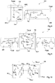
- the figure 2 schematically illustrates an embodiment of an improved random access static random access memory cell including transistors, particularly insulated gate field effect transistors more commonly referred to as MOSFET (Metal Oxide Semiconductor Field Effect). made in a stack of an electronic circuit on two levels of the stack.
- the memory cell comprises transistors located in a higher level N SUP which have a threshold voltage which can be modulated, the channel of each of these transistors being electrically coupled to a node of the electronic circuit of a lower level N INF by the Electrically conductive vias intermediate 22.
- Such a structure provides advantages especially in terms of size, and the ability to dynamically change the threshold voltage of some of the transistors to improve their performance. electrical characteristics such as stability and / or consumption.
- the Figures 3A and 3B are partial and schematic sectional views of embodiments of the SRAM cell 20, including a stack of layers.
- the layers of the stack 25 are divided into layers of the lower level N INF and layers of the upper level N SUP .
- the layer at the base of the stack is called a substrate 30.
- the substrate 30 may be a solid or semiconductor-on-insulator substrate, for example of the silicon on insulator or SOI (Silicon On Insulator) type, comprising a first a support layer which can be semiconductive and for example based on Si, covered by an insulating layer, for example based on SiO 2 , itself covered by a semiconductor layer, for example based on Si, and in which one or several active areas are likely to be formed.
- SOI Silicon On Insulator
- a first transistor T INF is formed in and on the substrate 30.
- the first transistor T INF comprises a source region 32, a drain region 34, as well as a channel zone 36, connecting the source region 32 and the region
- the first transistor T INF may optionally be formed on a SOI substrate totally deserted or partially deserted.
- the transistor T INF also comprises a gate 38 situated on a layer of dielectric material 37 of grid 38.
- the SRAM cell 20 also comprises at least one second transistor T SUP in a level N SUP of the stack higher than that of the level N INF in which the first transistor T INF is located .
- the second transistor T SUP comprises, in a semiconductor portion 50, a source region 52, a region drain 54, as well as a channel structure 56, connecting the source region 52 and the drain region 54.
- the second transistor T SUP also has a gate 58 resting on a gate dielectric layer 57.
- the second transistor T SUP is formed according to a completely depleted substrate-on-insulator technology or FDSOI (Fully Depleted Substrate On Insulator).
- the channel structure 56 is located above an electrically conductive track, preferably a metal track 60 of the last level of metallization of the lower level N INF and separated from the metal track 60 by an insulating zone Electrically 62.
- the insulating zone 62 is implemented so as to allow a coupling between the metal track 60 and the channel of the second transistor T SUP located above.
- this insulating zone 62 is in particular chosen to be much smaller than the thicknesses of the layers of interlevel dielectric materials in the electronic circuits according to the prior art, and which, in these electronic circuits, are intended to allow isolate between them different superimposed levels of components or lines of interconnections.
- the conductive track 60 thus makes it possible to control the channel potential of the transistor T SUP of the upper level N SUP .
- the entire semiconductor zone 56 of the channel of the second transistor T SUP is arranged facing the upper face or the top of the conductive track 60.
- the channel zone 56 of the second transistor T SUP may be made in a semiconductor layer of small thickness, so as to allow a static control at the inversion channel.
- small thickness it is meant that the channel region 56 of the second transistor T SUP may be formed in a semiconducting portion 50 having a thickness of, for example, between 1 nm and 100 nm, or for example between 5 nm and 20 nm.
- the thickness chosen for the semiconductor portion 50 in which the channel 56 is formed is provided in particular depending on the doping level of this layer to allow a completely depleted behavior.
- the thickness T sc of the channel zone 56 is equal to 7 nm, that the latter is made of silicon, that the thickness T ox of the dielectric zone 57 is equal to 1 nm, the latter is based on SiO 2 , Vdd is equal to 1 V, and the insulating zone 62 is SiO 2 , the insulating zone 62 is provided for example with a thickness of about 17.5 nm.
- the second transistor T SUP is formed according to a technology of the type partially on insulator depleted or PDSOI (acronym for Partially Depleted Substrate On Insulator).
- the conductive track 60 may be electrically connected to the semiconductor portion 50, for example by an electrically conductive via 64 outside the source region 52, the drain region 54, and the channel structure. 56. The conductive track 60 thus makes it possible to control the channel potential of the transistor T SUP of the upper level N SUP .
- the memory cell 20 may comprise a larger number of transistors, for example a number n (with n an integer such that n> 2) of transistors T 1 , T 2 ,..., T n superimposed, each transistor T k of a given level N k (with k an integer such that 1 ⁇ k ⁇ n) with a channel zone capable of being coupled to a conductive track of the level N k-1 less than the given level N k , this conducting track being located opposite said channel zone, at a distance sufficiently small to allow such coupling.
- the figure 4 is a circuit diagram of an embodiment of a memory cell 100 random access type 6T, that is to say with 6 transistors.
- the cell 100 comprises a plurality of transistors forming a first inverter and a second inverter, connected in a flip-flop configuration, commonly called flip-flop.
- the flip-flop comprises a first conduction transistor MD L and a second conduction transistor MD R , for example of the N-channel MOS type.
- the gate of the second conduction transistor MD R is connected to a first storage node N L of the cell 100 and the gate of the first conduction transistor MD L is connected to a second storage node N R of the cell 100.
- the sources of the conduction transistors MD L , MD R are connected to each other and to a source of a low reference potential Vss, for example mass.
- the drain of the first conduction transistor MD L is connected to the first node N L and the drain of the second conduction transistor MD R is connected to the second node N R.
- the flip-flop further comprises a first charge transistor ML L and a second charge transistor ML R , for example of the P-channel MOS type.
- the sources of the charge transistors ML L , ML R are connected to a source of charge.
- a high reference potential Vdd and the drain of the first load transistor ML L is connected to the first node N L and the drain of the second load transistor ML R is connected to the second node N R.
- the SRAM cell 100 also has a first access transistor MA L and a second access transistor MA R , for example N channel MOS transistors.
- the access transistors MA L and MA R have a grid connected to a word line WL.
- the source of the first access transistor MA L is connected to a first bit line BL L and the source of the second access transistor MA R is connected to a second bit line BL R.
- the drain of the first access transistor MA L is connected to the first storage node N L and the drain of the second access transistor MA R is connected to the second storage node N R.
- the access transistors MA L , MA R are arranged to allow access to the storage nodes N L and N R , during a read or write phase of the cell 100, and to block the access of the cell 100 when the cell 100 is in an information retention mode.
- the conduction transistors MD L , MD R and load ML L , ML R are provided to maintain a load necessary for the establishment of a given logic level, for example '0', corresponding for example to a potential equal to the potential Vss, or '1' corresponding, for example, to a potential equal to the potential Vdd, on one of the nodes N L or N R , as a function of the logic value stored in the cell 100.
- the figure 5 illustrates an embodiment of a SRAM 200 memory cell with six transistors, the transistors of which are distributed over two levels N INF and N SUP and in which a method of reading assistance is implemented.
- the SRAM memory cell 200 comprises all the elements of the memory cell 100 represented in FIG. figure 4 .
- the N-channel MOS transistors MA L , MA R , MD L and MD R are located in the lower level N INF and the P-channel MOS transistors ML L and ML R are located in the upper level N SUP .
- the channel region of the first charge transistor ML L is coupled to the second storage node N R and the channel area of the second charge transistor ML R is coupled to the first storage node N L , which which is schematically represented in figure 5 by dashed lines.
- the threshold voltage of the first load transistor ML L depends on the data stored in the second storage node N R and the threshold voltage of the second load transistor ML R depends on the data stored in the first storage node N L.
- the present embodiment allows to lower the threshold voltage of the P-channel MOS transistor used to raise the internal storage node to Vdd (and thus store the logic value '1').
- Bit lines BL L and BL R are preloaded to Vdd before the read operation.
- the word line WL is then biased to Vdd to access the data stored in the storage nodes N L , N R via the bit lines BL L and BL R.
- the access transistors MA L and MA R are then in a conductive state.
- the first node N L is at a high logic level, for example at the potential Vdd
- the second node N R is at a low logic level, for example at 0 V
- a conduction current is established between the bit line BL R and the mass Vss via the second conduction transistor MD R and the second access transistor MA R causing a discharge of the bit line BL R towards ground.
- This voltage drop on the bit line BL R causes a voltage difference between the bit lines BL L and BL R and the detection of this difference completes the reading through a sense amplifier.
- the discharge of the bit line BL R towards ground causes a rise in voltage at the second storage node N R. This rise in voltage must not change the state of the cell.
- the first load transistor ML L is made more conductive, this prevents it from being closed during the voltage rise of the second storage node N R. This improves the readability of the SRAM cell.
- the figure 6 illustrates an embodiment of a SRAM 210 memory cell with four transistors whose transistors are distributed over two levels N INF and N SUP and in which a support method for reading and retention is implemented.
- the SRAM memory cell 210 comprises all the elements of the memory cell 100 represented in FIG. figure 4 with the difference that the first conduction transistor MD L and the second conduction transistor MD R are not present.
- the N-channel MOS transistors MA L and MA R are located in the upper level N SUP and the P-channel MOS transistors ML L and ML R are located in the lower level N INF .
- the channel region of the first access transistor MA L is coupled to the second storage node N R and the channel area of the second access transistor MA R is coupled to the first storage node N L .
- the threshold voltage of the first access transistor MA L depends on the data stored in the second storage node N R and the threshold voltage of the second access transistor MA R depends on the data stored in the first storage node N L.
- the present embodiment makes it possible to increase the threshold voltage of the access transistor connected to the internal node in which the logic value '1' is stored.
- the bit lines BL L and BL R are preloaded at 0 V and the access transistors MA L and MA R are brought into a conductive state.
- the threshold voltage of the first access transistor MA L is increased, which makes it less conductive .
- the potential at node NL is then better maintained in a high logical state, thereby increasing the stability of the read operation.
- An operating mode of the cell 210 will now be described during a retention operation, that is to say in the absence of read or write operation in the cell.
- the bit lines BL L and BL R are preloaded at 0 V and the access transistors MA L and MA R are then in a blocked state.
- the first node N L is at Vdd
- the second node N R is at 0 V
- the retention time of the memory cell 210 is then increased.
- the figure 7 illustrates an embodiment of a SRAM memory cell 220 having four transistors whose transistors are distributed over two levels N INF and N SUP and in which a retention and reading assistance method is implemented.
- the SRAM memory cell 220 comprises all the elements of the memory cell 100 represented in FIG. figure 4 with the difference that the first load transistor ML L and the second load transistor ML R are not present, and that the access transistors MA L and MA R are P-channel MOS transistors.
- P-channel MOS transistors MA L and MA R are located in the upper level N SUP and the N-channel MOS transistors MD L and MD R are located in the lower level N INF .
- the channel region of the first access transistor MA L is coupled to the second storage node N R and the channel area of the second access transistor MA R is coupled to the first storage node N L .
- the threshold voltage of the first access transistor MA L depends on the data stored in the second storage node N R and the threshold voltage of the second access transistor MA R depends on the data stored in the first storage node N L.
- the present embodiment makes it possible to increase the threshold voltage of the access transistor connected to the internal node in which the logic value '0' is stored.
- the bit lines BL L and BL R are preloaded at Vdd and the access transistors MA L and MA R are brought into a conductive state.
- the first node N L is at Vdd
- the second node N R is at 0 V
- it is the threshold voltage of the second access transistor MA R P type is increased, which the makes it less conductive
- the stability of the read operation is thus improved because the node NR is better maintained at 0 V since it receives less current from the bit line BLR.
- An operating mode of the cell 220 will now be described during a retention operation, i.e. if there is no read or write operation in the cell.
- the bit lines BL L and BL R are preloaded at Vdd and the access transistors MA L and MA R are then in a blocked state.
- the first node N L is at Vdd
- the second node N R is at 0 V
- the retention time of the memory cell 220 is then increased.
- the figure 8 illustrates an embodiment of a SRAM 230 memory cell with eight transistors whose transistors are distributed over two levels and in which a read assistance method is implemented.
- the SRAM 8T 230 cell comprises the memory cell 100 represented in FIG. figure 4 and further comprises a read circuit 232 comprising two MOS transistors RPPG and RPPD which are both N-channel. Alternatively, the MOS transistors RPPG and RPPD may both be P-channel. N L storage of the SRAM 100 cell is connected to the gate of the RPPD transistor. The source of the transistor RPPD is connected to the ground Vss and the drain of the transistor RPPD is connected to the source of the transistor RPPG. The drain of the RPPG transistor is connected to a read bit line RBL and the gate of the RPPG transistor is connected to a read word line RWL.
- All the MOS transistors of the SRAM memory cell 100 are located in the lower level N INF and the MOS transistors RPPG and RPPD of the read circuit 232 are located in the upper level N SUP .
- the channel area of the MOS transistor RPPG and the channel area of the RPPD transistor are coupled to the first storage node N L. The present embodiment makes it possible to reduce the threshold voltage of the RPPG and RPPD transistors when the logic value '1' is stored in the storage node N L.
- the lines bit BL L and BL R are preloaded at Vdd and the access transistors MA L and MA R are brought into a conductive state.
- the transistor RPPD is activated and a path is created between the read bit line RBL and the ground Vss.
- the reading is completed with the detection (or not) of the voltage drop on the read bit line RBL.
- the RPPG and RPPD transistors being more conductive, this allows an accelerated discharge of the read bit line RBL in the case where the storage node N L stores the logical value '1'.
- the duration of a read operation can therefore be reduced. For a circuit containing such a memory and whose operating frequency can be limited by the duration of a reading operation in the memory, this increases the operating frequency of the circuit.
- the figure 9 illustrates an embodiment of an SRAM memory cell 240 of a content-addressable memory whose transistors are distributed over two levels and in which a reading assistance method is implemented.
- the SRAM 8T 240 cell comprises first and second memory cells 100 as represented in FIG. figure 4 and further comprises an exclusive OR logic gate 242, also called XOR gate.
- the logic gate 242 comprises two N-channel MOS transistors X1 and X3.
- the second storage node N R1 of the first SRAM cell is connected to the gate of the transistor X3.
- the source of the transistor X3 is connected to the ground Vss and the drain of the transistor X3 is connected to the source of the transistor X1.
- the gate of transistor X1 is connected to a read bit line SLT and the drain of transistor X1 is connected to a read word line ML.
- the logic gate 242 further comprises two N-channel MOS transistors X2 and X4.
- the first storage node N L2 of the second SRAM cell is connected to the gate of the transistor X4.
- the source of the transistor X4 is connected to the ground Vss and the drain of the transistor X4 is connected to the source of the transistor X2.
- the gate of transistor X2 is connected to a read bit line SLF and the drain of transistor X2 is connected to the read word line ML. All the MOS transistors of the first and second SRAM memory cells 100 are located in the lower level N INF and the MOS transistors of the logic gate 242 are located in the upper level N SUP .
- the values stored in the first and second memory cells 6T 100 determine the value stored in the memory cell 240. For example, if the logic value '0' is stored at the second storage node N R1 of the first memory cell and if the logical value '1' is stored at the first storage node N L2 of the second memory cell, then it is considered that the logic value '0' is stored in the memory cell 240. In addition, if the logic value '1' is stored at the second storage node N R1 of the first memory cell and if the logical value '0' is stored at the first storage node N L2 of the second memory cell, then it is considered that the logical value '1' is stored in the memory cell 240.
- the XOR gate 242 makes it possible to compare the value sought and the value stored in the memory cell 240.
- the value sought is transmitted to the memory cell 240 on the read bit line SLT and its complement on the bit line SLF. .
- a read operation in which the data sought corresponds to the data stored in the memory cell 240 is called a success ("match" in English) and a read operation in which the data sought does not correspond to the data stored in the cell memory 240 is called a failure ("miss" in English).
- the read word line ML is preloaded to Vdd. If a failure occurs, the read word line ML is unloaded via at least one of two branches of the XOR gate 242.
- the discharge time defines the speed of the read operation.
- the present embodiment makes it possible to reduce the threshold voltage of the transistors X1 and X2 in the case of failure, which reduces the duration of the read operation.
- the supply voltage of the memory cells can be decreased.
- the figure 10 illustrates an embodiment of a SRAM 250 memory cell with six transistors whose transistors are distributed over two levels and in which a write assistance method is implemented.
- the SRAM memory cell 250 comprises all the elements of the memory cell 200 represented in FIG. figure 5 with the difference that the channel region of the first charge transistor ML L is coupled to the second bit line BL R and the channel area of the second charge transistor ML R is coupled to the first bit line BL L.
- the threshold voltage of the first load transistor ML L depends on the data present on the second bit line BL R and the threshold voltage of the second load transistor ML R depends on the data present on the first bit line BL L.
- the present embodiment makes it possible to increase the threshold voltage of the load transistor connected to the bit line on which the logic value '0' is present and to reduce the threshold voltage of the load transistor connected to the bit line. where the logical value '1' is present.
- a write operation is to change the state of the first storage node N L from '1' to '0' and to change the state of the second storage node N R from '0' to '1'.
- the first bit line BL L is preloaded to Vss and the second bit line BL R is preloaded to Vdd.
- the access transistors MA L and MA R are then brought to the state driver.
- a conduction path is created between the first storage node N L and the first bit line BL L via the first access transistor MA L and a conduction path is created between the second storage node N R and the second line bit BL R via the second access transistor MA R.
- the first storage node N L discharges to the first bit line BL L and the second bit line BL R discharges to the second storage node N R. Since the threshold voltage of the second charge transistor ML R is reduced and the threshold voltage of the first charge transistor ML L is increased, this facilitates the closing of the first charge transistor ML L during the voltage rise of the second storage node. N R and the passing state of the second charge transistor ML R during the voltage decrease of the first storage node N L. The write stability of the SRAM cell 250 is thus increased.
- the figure 11 illustrates an embodiment of a SRAM 260 four-transistor memory cell whose transistors are distributed over two levels and in which a write assistance method is implemented.
- the SRAM memory cell 260 comprises all the elements of the memory cell 250 represented in FIG. figure 10 with the difference that the conduction transistors MD L and MD R are not present.
- the channel region of the first load transistor ML L is coupled to the second bit line BL R and the channel area of the second load transistor ML R is coupled to the first bit line BL L .
- the mode of operation of the cell 260 is the same as previously described for the memory cell 250.
- the write stability of the SRAM cell 260 is increased.
- the figure 12 illustrates an embodiment of a SRAM 270 memory cell with four transistors whose transistors are distributed over two levels and in which a write assistance method is implemented.
- the SRAM memory cell 270 comprises all the elements of the memory cell 250 represented in FIG. figure 10 with the difference that transistors ML L and ML R are not present, that the access transistors MA L and MA R are P-channel MOS transistors, that the P-channel MOS transistors MA L and MA R are located in the lower level N INF and the N-channel MOS MD L and MD R transistors are located in the upper N SUP level .
- the channel region of the first conduction transistor MD L is coupled to the second bit line BL R and the channel region of the second conduction transistor MD R is coupled to the first bit line BL L .
- the threshold voltage of the first conduction transistor MD L depends on the data present on the second bit line BL R and the threshold voltage of the second conduction transistor MD R depends on the data present on the first bit line BL L.
- the present embodiment makes it possible to increase the threshold voltage of the conduction transistor connected to the bit line on which the logic value '1' is present and to reduce the threshold voltage of the conduction transistor connected to the bit line. where the logical value '0' is present.
- the duration of a write operation can be reduced. For a circuit containing such a memory and whose operating frequency is limited by the duration of a write operation in the memory, this increases the operating frequency of the circuit.
- the figure 13 partially and schematically shows an embodiment of an SRAM memory comprising a plurality of memory cells.
- the memory cells of the memory are made in different levels Niv 1 to Niv N of a stack of layers where N is an integer, for example between 2 and 128, the level Niv 1 being the level at the base of the stack and level Niv N being the level at the top of the stack.
- Each level may comprise MOS transistors and metal tracks of at least one metallization level.
- the electrically conductive material composing the metal tracks of the last level of metallization may be different from one level of the stack to another.
- the electrically insulating material constituting the insulating layers on which the conductive tracks are formed may be different from one level of the stack to another.
- the metal tracks of the last level of metallization are made of copper and for the other levels Niv 1 to Niv N-1 , the metal tracks of the last level of metallization are in tungsten.
- the electrically insulating material constituting the insulating layers is a so-called low-k material and for the other levels Niv 1 to Niv N-1 , the electrically insulating material constituting the insulating layers is SiO 2 .
- a low-k material is a material whose dielectric constant is less than 3.9. It is generally not possible to make metal tracks from level 1 to level 1 in copper N to 1 to avoid pollution risks when forming conductive layers of a higher level.
- the figure 14 represents a circuit diagram of an example of an SRAM memory in which the SRAM memory cells are arranged in M rows and in P columns where M and P are integers.
- the memory comprises, for each row, a word line WLj, where j is an integer ranging between 0 and M-1, which is connected to all the memory cells of the row.
- the memory comprises, for each column, two bit lines BL Lk and BL Rk , k being an integer varying between 0 and P-1, which are connected to all the memory cells of the column.
- FIGs 15 and 16 represent one embodiment of a memory 300 on two levels Level 1 and Level 2 of a stack and having an equivalent circuit diagram corresponds to the diagram shown in figure 14 .
- figure 15 we have only very schematically represented two memory cells of the memory and on the figure 16 only the bit lines of the memory have been represented.
- the memory cells of the memory 300 are divided into the two levels Lvl 1 and Lvl 2 .
- the memory cells of the higher level Niv 2 are arranged in M / 2 rows and in P columns.
- k is an integer ranging from 0 to P-1
- two bit lines GBLT k and GBLF k formed by conductor tracks of the upper level Level 2 are connected to the upper level memory cells Lv 2 belonging to the column under consideration.
- the memory cells of the lower level Level 1 also belonging to the considered column are connected to bit lines GBLT k and GBLF k by interconnections LBLT k, j and lblF k, j that connect the memory cells of the lower level Level 1 to tracks Metallic Level Levels Level 2 .
- a word line WL_TOP j formed by a conductive track of the higher level Niv 2 , is connected to the upper level memory cells. 2 belonging to the row in question and a word line WL_BOT j , formed by a conductive track of the lower level Niv 1 , is connected to the memory cells of the lower level Niv 1 belonging to the row in question.
- Level 1 Level (Level 2 respectively) can itself be divided into a lower sub-level N INF and an upper sub-level N SUP.
- the transistors of a memory cell of the level Niv 1 (respectively Niv 2 ) can then be distributed on the two sub-levels N INF and N SUP according to one of the structures described above in relation to the Figures 5 to 12 .
- the memory cells are distributed on two levels Niv 1 and Niv 2 , it is clear that the cells of the memory can be distributed on more than two levels.
- the longer metal tracks of the memory 300 which correspond to the GBLT K and GBLF k word lines are advantageously formed in the upper level Lv 2 and can therefore be formed of a material which is a good electrical conductor.
- the GBLT K and GBLF k bit lines are made of copper and the LBLT k, j and LBLF k interconnections are made of tungsten. With such an organization, the access to the memory cells of the lower level N INF is not affected by the use of tungsten in the interconnections and silicon dioxide SiO 2 for the dielectric of the lower levels.
- An important advantage of the architecture realized on at least two levels, in addition to the density gains, is that it makes it possible to significantly reduce the lengths of the conductive tracks forming the bit lines and the word lines.
- the length of the GBLT k and GBLF k bit lines is reduced compared to a memory made in a single level.
- the speed of a write operation of the memory 300 represented on the Figures 14 and 15 can be increased.
- the figure 17 illustrates an embodiment of a SRAM 310 memory cell with six transistors whose transistors are distributed on two levels N INF and N SUP and in which a reading assistance method is implemented.
- the SRAM memory cell 310 comprises all the elements of the memory cell 100 represented in FIG. figure 4 .
- the N-channel MOS transistors MA L , MA R , MD L and MD R are located in the upper level N SUP and the P-channel MOS transistors ML L and ML R are located in the lower level N INF .
- an additional word line WL ' is provided in the lower level N INF and receives the same voltage as that applied on the word line WL.
- the channel regions of the first and second access transistors MA L and MA R are coupled to the additional word line WL ', which is schematically represented in FIG. figure 17 by dashed lines.
- the present embodiment makes it possible to increase the threshold voltage of the access transistors MA L and MA R when the word line WL 'is at' 0 'and to reduce the threshold voltage of the access transistors MA L and MA R when the word line WL 'is at' 1 '.
- the figure 18 illustrates an embodiment of an SRAM memory cell 320 of a content-addressable memory whose transistors are distributed over two levels N INF and N SUP and in which a reading assistance method is implemented.
- the SRAM memory cell 320 comprises all the elements of the memory cell 240 represented in FIG.
- the channel region of transistor X3 can be coupled or connected as shown in FIG. figure 9 or may alternatively be coupled to the read bit line SLT '.
- the channel region of transistor X4 can be coupled as shown in FIG. figure 9 or may alternatively be coupled to the read bit line SLF '.
- the figure 19 is a diagram similar to the figure 15 illustrating another embodiment of a SRAM 330 on two levels.
- the memory 330 comprises all the memory elements 300 represented on the Figures 15 and 16 and further comprises an additional level Level 3 wherein there is provided the two bit lines GBLT k and GBLF k, a bit SWT kj connected to the line switch GBLT k and SWF switch kj connected to the GBLF bit line k, the memory cells of the lower level Niv 2 also belonging to the column in question are respectively connected to the switches SWT kj and SWT kj by interconnections LBLT ' kj and LBLF' kj .
- the memory cells of the lower levels Niv 1 and Niv 2 belonging to the column in question are therefore connected to the GBLT k and GBLF k bit lines by the interconnects LBLT k, j , LBLF kj , LBLT ' kj , LBLF' kj which connect the cells memory of lower levels Lvl 1 and Lvl 2 at switches SWTkj and SWFkj of the higher level Lvl 3 .
- the switches SWTkj and SWFkj are controlled by a selection line WL_SEL j . This makes it possible to isolate the cells of the GBLT k and GBLF k bit lines during read and / or write operations.
- the figure 20 is a perspective view, partial and schematic, of an embodiment of the SRAM memory cell of the figure 7 on two levels N INF and N SUP .
- the couplings of the channel regions of the transistors MA L and MA R are not represented.
- the regions R correspond to active semiconductor regions
- the tracks in solid lines correspond to tracks conductors formed directly on the active regions
- the dashed tracks correspond to conductive tracks of a first metallization level
- the mixed-line track corresponds to a conductive track of a second level of metallization.
- the elements V are conductive vias connecting elements of the level N INF to elements of the level N SUP .
Landscapes
- Engineering & Computer Science (AREA)
- Microelectronics & Electronic Packaging (AREA)
- Computer Hardware Design (AREA)
- Power Engineering (AREA)
- Physics & Mathematics (AREA)
- Condensed Matter Physics & Semiconductors (AREA)
- General Physics & Mathematics (AREA)
- Semiconductor Memories (AREA)
- Static Random-Access Memory (AREA)
Applications Claiming Priority (1)
| Application Number | Priority Date | Filing Date | Title |
|---|---|---|---|
| FR1752529A FR3064396B1 (fr) | 2017-03-27 | 2017-03-27 | Cellule memoire sram |
Publications (2)
| Publication Number | Publication Date |
|---|---|
| EP3382709A1 true EP3382709A1 (de) | 2018-10-03 |
| EP3382709B1 EP3382709B1 (de) | 2020-11-18 |
Family
ID=59031144
Family Applications (1)
| Application Number | Title | Priority Date | Filing Date |
|---|---|---|---|
| EP18164392.5A Active EP3382709B1 (de) | 2017-03-27 | 2018-03-27 | Sram-speicherzelle |
Country Status (3)
| Country | Link |
|---|---|
| US (1) | US20180277197A1 (de) |
| EP (1) | EP3382709B1 (de) |
| FR (1) | FR3064396B1 (de) |
Families Citing this family (2)
| Publication number | Priority date | Publication date | Assignee | Title |
|---|---|---|---|---|
| FR3083912A1 (fr) * | 2018-07-13 | 2020-01-17 | Commissariat A L'energie Atomique Et Aux Energies Alternatives | Memoire sram / rom reconfigurable par polarisation de substrat |
| US11348928B1 (en) * | 2021-03-03 | 2022-05-31 | Micron Technology, Inc. | Thin film transistor random access memory |
Citations (4)
| Publication number | Priority date | Publication date | Assignee | Title |
|---|---|---|---|---|
| JPH04170069A (ja) * | 1990-11-02 | 1992-06-17 | Hitachi Ltd | 半導体記憶装置 |
| EP2131397A1 (de) * | 2008-06-02 | 2009-12-09 | Commissariat a L'Energie Atomique | In drei Richtungen integrierter Transistorschaltkreis mit einer dynamisch anpassbaren Schwellenspannung (VT) |
| WO2014185085A1 (ja) * | 2013-05-14 | 2014-11-20 | 株式会社 東芝 | 半導体記憶装置 |
| WO2014209278A1 (en) * | 2013-06-25 | 2014-12-31 | Intel Corporation | Monolithic three-dimensional (3d) ics with local inter-level interconnects |
Family Cites Families (6)
| Publication number | Priority date | Publication date | Assignee | Title |
|---|---|---|---|---|
| JP4038351B2 (ja) * | 2001-05-29 | 2008-01-23 | 株式会社東芝 | 半導体記憶装置 |
| JP4855786B2 (ja) * | 2006-01-25 | 2012-01-18 | 株式会社東芝 | 半導体装置 |
| US7400523B2 (en) * | 2006-06-01 | 2008-07-15 | Texas Instruments Incorporated | 8T SRAM cell with higher voltage on the read WL |
| FR2910999B1 (fr) * | 2006-12-28 | 2009-04-03 | Commissariat Energie Atomique | Cellule memoire dotee de transistors double-grille, a grilles independantes et asymetriques |
| US8395191B2 (en) * | 2009-10-12 | 2013-03-12 | Monolithic 3D Inc. | Semiconductor device and structure |
| JP5826716B2 (ja) * | 2012-06-19 | 2015-12-02 | 株式会社東芝 | 半導体装置及びその製造方法 |
-
2017
- 2017-03-27 FR FR1752529A patent/FR3064396B1/fr not_active Expired - Fee Related
-
2018
- 2018-03-27 EP EP18164392.5A patent/EP3382709B1/de active Active
- 2018-03-27 US US15/937,454 patent/US20180277197A1/en not_active Abandoned
Patent Citations (4)
| Publication number | Priority date | Publication date | Assignee | Title |
|---|---|---|---|---|
| JPH04170069A (ja) * | 1990-11-02 | 1992-06-17 | Hitachi Ltd | 半導体記憶装置 |
| EP2131397A1 (de) * | 2008-06-02 | 2009-12-09 | Commissariat a L'Energie Atomique | In drei Richtungen integrierter Transistorschaltkreis mit einer dynamisch anpassbaren Schwellenspannung (VT) |
| WO2014185085A1 (ja) * | 2013-05-14 | 2014-11-20 | 株式会社 東芝 | 半導体記憶装置 |
| WO2014209278A1 (en) * | 2013-06-25 | 2014-12-31 | Intel Corporation | Monolithic three-dimensional (3d) ics with local inter-level interconnects |
Also Published As
| Publication number | Publication date |
|---|---|
| US20180277197A1 (en) | 2018-09-27 |
| FR3064396B1 (fr) | 2019-04-19 |
| EP3382709B1 (de) | 2020-11-18 |
| FR3064396A1 (fr) | 2018-09-28 |
Similar Documents
| Publication | Publication Date | Title |
|---|---|---|
| EP2131396A1 (de) | SRAM-Speicherzelle mit auf verschiedenen Ebenen integrierten Transistoren, deren VT-Schwellenspannung dynamisch anpassbar ist | |
| EP2245632B1 (de) | Sram-speicherzelle auf basis von doppelgate-transistoren mit mittel zur erweiterung eines schreibbereichs | |
| FR2774209A1 (fr) | Procede de controle du circuit de lecture d'un plan memoire et dispositif de memoire correspondant | |
| FR2923646A1 (fr) | Cellule memoire sram dotee de transistors a structure multi-canaux verticale | |
| EP3002788B1 (de) | Vorrichtung mit sram-speicherzellen die mitteln zur polarisierung der wannen der speicherzelltransistoren umfasst | |
| EP3010022B1 (de) | Speicherzelle mit lese-transistoren vom typ tfet und mosfet | |
| EP1388896A1 (de) | Speicher vom Silizium-auf-Isolator Typ | |
| FR3074604A1 (fr) | Memoire sram a effacement rapide | |
| EP3382709B1 (de) | Sram-speicherzelle | |
| FR2517143A1 (fr) | Bascule bistable a stockage non volatil et a repositionnement dynamique | |
| EP0121464A1 (de) | Nichtflüchtige RAM Speicherzelle mit CMOS Transistoren mit gemeinsamem schwebendem Gate | |
| FR2979738A1 (fr) | Memoire sram a circuits d'acces en lecture et en ecriture separes | |
| FR2775382A1 (fr) | Procede de controle du rafraichissement d'un plan memoire d'un dispositif de memoire vive dynamique, et dispositif de memoire vive correspondant | |
| EP3373303A1 (de) | Tfet-speicherlatch ohne aktualisierung | |
| FR2884346A1 (fr) | Dispositif de memoire du type programmable une fois, et procede de programmation | |
| FR2875328A1 (fr) | Cellule memoire sram protegee contre des pics de courant ou de tension | |
| FR2955195A1 (fr) | Dispositif de comparaison de donnees dans une memoire adressable par contenu sur seoi | |
| EP3896695B1 (de) | Verfahren zum schreiben in einen nichtflüchtigen speicher in abhängigkeit von der alterung der speicherzellen und entsprechender integrierter schaltkreis | |
| EP2977988B1 (de) | Nicht-flüchtiger speicher mit programmierbarem widerstand | |
| EP4020479A1 (de) | Differentielles lesen eines rram-speichers mit geringem stromverbrauch | |
| CN110956991B (zh) | 感测放大器、存储器装置及形成存储器装置的方法 | |
| EP3451340B1 (de) | Programmierungsverfahren einer dram-speicherzelle mit einem transistor, und speichervorrichtung | |
| EP3594951B1 (de) | Sram-/rom-speicher, der durch substratvorspannung rekonfigurierbar ist | |
| EP3832719A1 (de) | 3d-speichervorrichtung mit speicherzellen vom typ sram mit einstellbarer rückseitiger polarisation | |
| FR3027442A1 (fr) | Cellule memoire a transistors tfet de memorisation polarises en inverse |
Legal Events
| Date | Code | Title | Description |
|---|---|---|---|
| PUAI | Public reference made under article 153(3) epc to a published international application that has entered the european phase |
Free format text: ORIGINAL CODE: 0009012 |
|
| STAA | Information on the status of an ep patent application or granted ep patent |
Free format text: STATUS: REQUEST FOR EXAMINATION WAS MADE |
|
| 17P | Request for examination filed |
Effective date: 20180327 |
|
| AK | Designated contracting states |
Kind code of ref document: A1 Designated state(s): AL AT BE BG CH CY CZ DE DK EE ES FI FR GB GR HR HU IE IS IT LI LT LU LV MC MK MT NL NO PL PT RO RS SE SI SK SM TR |
|
| AX | Request for extension of the european patent |
Extension state: BA ME |
|
| STAA | Information on the status of an ep patent application or granted ep patent |
Free format text: STATUS: EXAMINATION IS IN PROGRESS |
|
| 17Q | First examination report despatched |
Effective date: 20190319 |
|
| GRAP | Despatch of communication of intention to grant a patent |
Free format text: ORIGINAL CODE: EPIDOSNIGR1 |
|
| STAA | Information on the status of an ep patent application or granted ep patent |
Free format text: STATUS: GRANT OF PATENT IS INTENDED |
|
| INTG | Intention to grant announced |
Effective date: 20200715 |
|
| GRAS | Grant fee paid |
Free format text: ORIGINAL CODE: EPIDOSNIGR3 |
|
| GRAA | (expected) grant |
Free format text: ORIGINAL CODE: 0009210 |
|
| STAA | Information on the status of an ep patent application or granted ep patent |
Free format text: STATUS: THE PATENT HAS BEEN GRANTED |
|
| AK | Designated contracting states |
Kind code of ref document: B1 Designated state(s): AL AT BE BG CH CY CZ DE DK EE ES FI FR GB GR HR HU IE IS IT LI LT LU LV MC MK MT NL NO PL PT RO RS SE SI SK SM TR |
|
| REG | Reference to a national code |
Ref country code: GB Ref legal event code: FG4D Free format text: NOT ENGLISH |
|
| REG | Reference to a national code |
Ref country code: CH Ref legal event code: EP |
|
| REG | Reference to a national code |
Ref country code: IE Ref legal event code: FG4D Free format text: LANGUAGE OF EP DOCUMENT: FRENCH |
|
| REG | Reference to a national code |
Ref country code: DE Ref legal event code: R096 Ref document number: 602018009731 Country of ref document: DE |
|
| REG | Reference to a national code |
Ref country code: AT Ref legal event code: REF Ref document number: 1336642 Country of ref document: AT Kind code of ref document: T Effective date: 20201215 |
|
| REG | Reference to a national code |
Ref country code: AT Ref legal event code: MK05 Ref document number: 1336642 Country of ref document: AT Kind code of ref document: T Effective date: 20201118 |
|
| REG | Reference to a national code |
Ref country code: NL Ref legal event code: MP Effective date: 20201118 |
|
| PG25 | Lapsed in a contracting state [announced via postgrant information from national office to epo] |
Ref country code: FI Free format text: LAPSE BECAUSE OF FAILURE TO SUBMIT A TRANSLATION OF THE DESCRIPTION OR TO PAY THE FEE WITHIN THE PRESCRIBED TIME-LIMIT Effective date: 20201118 Ref country code: PT Free format text: LAPSE BECAUSE OF FAILURE TO SUBMIT A TRANSLATION OF THE DESCRIPTION OR TO PAY THE FEE WITHIN THE PRESCRIBED TIME-LIMIT Effective date: 20210318 Ref country code: RS Free format text: LAPSE BECAUSE OF FAILURE TO SUBMIT A TRANSLATION OF THE DESCRIPTION OR TO PAY THE FEE WITHIN THE PRESCRIBED TIME-LIMIT Effective date: 20201118 Ref country code: NO Free format text: LAPSE BECAUSE OF FAILURE TO SUBMIT A TRANSLATION OF THE DESCRIPTION OR TO PAY THE FEE WITHIN THE PRESCRIBED TIME-LIMIT Effective date: 20210218 Ref country code: GR Free format text: LAPSE BECAUSE OF FAILURE TO SUBMIT A TRANSLATION OF THE DESCRIPTION OR TO PAY THE FEE WITHIN THE PRESCRIBED TIME-LIMIT Effective date: 20210219 |
|
| PG25 | Lapsed in a contracting state [announced via postgrant information from national office to epo] |
Ref country code: AT Free format text: LAPSE BECAUSE OF FAILURE TO SUBMIT A TRANSLATION OF THE DESCRIPTION OR TO PAY THE FEE WITHIN THE PRESCRIBED TIME-LIMIT Effective date: 20201118 Ref country code: BG Free format text: LAPSE BECAUSE OF FAILURE TO SUBMIT A TRANSLATION OF THE DESCRIPTION OR TO PAY THE FEE WITHIN THE PRESCRIBED TIME-LIMIT Effective date: 20210218 Ref country code: IS Free format text: LAPSE BECAUSE OF FAILURE TO SUBMIT A TRANSLATION OF THE DESCRIPTION OR TO PAY THE FEE WITHIN THE PRESCRIBED TIME-LIMIT Effective date: 20210318 Ref country code: LV Free format text: LAPSE BECAUSE OF FAILURE TO SUBMIT A TRANSLATION OF THE DESCRIPTION OR TO PAY THE FEE WITHIN THE PRESCRIBED TIME-LIMIT Effective date: 20201118 Ref country code: PL Free format text: LAPSE BECAUSE OF FAILURE TO SUBMIT A TRANSLATION OF THE DESCRIPTION OR TO PAY THE FEE WITHIN THE PRESCRIBED TIME-LIMIT Effective date: 20201118 Ref country code: SE Free format text: LAPSE BECAUSE OF FAILURE TO SUBMIT A TRANSLATION OF THE DESCRIPTION OR TO PAY THE FEE WITHIN THE PRESCRIBED TIME-LIMIT Effective date: 20201118 |
|
| REG | Reference to a national code |
Ref country code: LT Ref legal event code: MG9D |
|
| PG25 | Lapsed in a contracting state [announced via postgrant information from national office to epo] |
Ref country code: HR Free format text: LAPSE BECAUSE OF FAILURE TO SUBMIT A TRANSLATION OF THE DESCRIPTION OR TO PAY THE FEE WITHIN THE PRESCRIBED TIME-LIMIT Effective date: 20201118 |
|
| PG25 | Lapsed in a contracting state [announced via postgrant information from national office to epo] |
Ref country code: SM Free format text: LAPSE BECAUSE OF FAILURE TO SUBMIT A TRANSLATION OF THE DESCRIPTION OR TO PAY THE FEE WITHIN THE PRESCRIBED TIME-LIMIT Effective date: 20201118 Ref country code: EE Free format text: LAPSE BECAUSE OF FAILURE TO SUBMIT A TRANSLATION OF THE DESCRIPTION OR TO PAY THE FEE WITHIN THE PRESCRIBED TIME-LIMIT Effective date: 20201118 Ref country code: CZ Free format text: LAPSE BECAUSE OF FAILURE TO SUBMIT A TRANSLATION OF THE DESCRIPTION OR TO PAY THE FEE WITHIN THE PRESCRIBED TIME-LIMIT Effective date: 20201118 Ref country code: LT Free format text: LAPSE BECAUSE OF FAILURE TO SUBMIT A TRANSLATION OF THE DESCRIPTION OR TO PAY THE FEE WITHIN THE PRESCRIBED TIME-LIMIT Effective date: 20201118 Ref country code: RO Free format text: LAPSE BECAUSE OF FAILURE TO SUBMIT A TRANSLATION OF THE DESCRIPTION OR TO PAY THE FEE WITHIN THE PRESCRIBED TIME-LIMIT Effective date: 20201118 Ref country code: SK Free format text: LAPSE BECAUSE OF FAILURE TO SUBMIT A TRANSLATION OF THE DESCRIPTION OR TO PAY THE FEE WITHIN THE PRESCRIBED TIME-LIMIT Effective date: 20201118 |
|
| REG | Reference to a national code |
Ref country code: DE Ref legal event code: R097 Ref document number: 602018009731 Country of ref document: DE |
|
| PG25 | Lapsed in a contracting state [announced via postgrant information from national office to epo] |
Ref country code: DK Free format text: LAPSE BECAUSE OF FAILURE TO SUBMIT A TRANSLATION OF THE DESCRIPTION OR TO PAY THE FEE WITHIN THE PRESCRIBED TIME-LIMIT Effective date: 20201118 |
|
| PLBE | No opposition filed within time limit |
Free format text: ORIGINAL CODE: 0009261 |
|
| STAA | Information on the status of an ep patent application or granted ep patent |
Free format text: STATUS: NO OPPOSITION FILED WITHIN TIME LIMIT |
|
| REG | Reference to a national code |
Ref country code: DE Ref legal event code: R119 Ref document number: 602018009731 Country of ref document: DE |
|
| 26N | No opposition filed |
Effective date: 20210819 |
|
| PG25 | Lapsed in a contracting state [announced via postgrant information from national office to epo] |
Ref country code: NL Free format text: LAPSE BECAUSE OF FAILURE TO SUBMIT A TRANSLATION OF THE DESCRIPTION OR TO PAY THE FEE WITHIN THE PRESCRIBED TIME-LIMIT Effective date: 20201118 Ref country code: AL Free format text: LAPSE BECAUSE OF FAILURE TO SUBMIT A TRANSLATION OF THE DESCRIPTION OR TO PAY THE FEE WITHIN THE PRESCRIBED TIME-LIMIT Effective date: 20201118 Ref country code: IT Free format text: LAPSE BECAUSE OF FAILURE TO SUBMIT A TRANSLATION OF THE DESCRIPTION OR TO PAY THE FEE WITHIN THE PRESCRIBED TIME-LIMIT Effective date: 20201118 Ref country code: MC Free format text: LAPSE BECAUSE OF FAILURE TO SUBMIT A TRANSLATION OF THE DESCRIPTION OR TO PAY THE FEE WITHIN THE PRESCRIBED TIME-LIMIT Effective date: 20201118 |
|
| REG | Reference to a national code |
Ref country code: CH Ref legal event code: PL |
|
| PG25 | Lapsed in a contracting state [announced via postgrant information from national office to epo] |
Ref country code: SI Free format text: LAPSE BECAUSE OF FAILURE TO SUBMIT A TRANSLATION OF THE DESCRIPTION OR TO PAY THE FEE WITHIN THE PRESCRIBED TIME-LIMIT Effective date: 20201118 |
|
| REG | Reference to a national code |
Ref country code: BE Ref legal event code: MM Effective date: 20210331 |
|
| PG25 | Lapsed in a contracting state [announced via postgrant information from national office to epo] |
Ref country code: LU Free format text: LAPSE BECAUSE OF NON-PAYMENT OF DUE FEES Effective date: 20210327 Ref country code: LI Free format text: LAPSE BECAUSE OF NON-PAYMENT OF DUE FEES Effective date: 20210331 Ref country code: IE Free format text: LAPSE BECAUSE OF NON-PAYMENT OF DUE FEES Effective date: 20210327 Ref country code: CH Free format text: LAPSE BECAUSE OF NON-PAYMENT OF DUE FEES Effective date: 20210331 Ref country code: DE Free format text: LAPSE BECAUSE OF NON-PAYMENT OF DUE FEES Effective date: 20211001 Ref country code: FR Free format text: LAPSE BECAUSE OF NON-PAYMENT OF DUE FEES Effective date: 20210331 Ref country code: ES Free format text: LAPSE BECAUSE OF FAILURE TO SUBMIT A TRANSLATION OF THE DESCRIPTION OR TO PAY THE FEE WITHIN THE PRESCRIBED TIME-LIMIT Effective date: 20201118 |
|
| PG25 | Lapsed in a contracting state [announced via postgrant information from national office to epo] |
Ref country code: IS Free format text: LAPSE BECAUSE OF FAILURE TO SUBMIT A TRANSLATION OF THE DESCRIPTION OR TO PAY THE FEE WITHIN THE PRESCRIBED TIME-LIMIT Effective date: 20210318 |
|
| PG25 | Lapsed in a contracting state [announced via postgrant information from national office to epo] |
Ref country code: BE Free format text: LAPSE BECAUSE OF NON-PAYMENT OF DUE FEES Effective date: 20210331 |
|
| GBPC | Gb: european patent ceased through non-payment of renewal fee |
Effective date: 20220327 |
|
| PG25 | Lapsed in a contracting state [announced via postgrant information from national office to epo] |
Ref country code: GB Free format text: LAPSE BECAUSE OF NON-PAYMENT OF DUE FEES Effective date: 20220327 |
|
| PG25 | Lapsed in a contracting state [announced via postgrant information from national office to epo] |
Ref country code: CY Free format text: LAPSE BECAUSE OF FAILURE TO SUBMIT A TRANSLATION OF THE DESCRIPTION OR TO PAY THE FEE WITHIN THE PRESCRIBED TIME-LIMIT Effective date: 20201118 |
|
| PG25 | Lapsed in a contracting state [announced via postgrant information from national office to epo] |
Ref country code: HU Free format text: LAPSE BECAUSE OF FAILURE TO SUBMIT A TRANSLATION OF THE DESCRIPTION OR TO PAY THE FEE WITHIN THE PRESCRIBED TIME-LIMIT; INVALID AB INITIO Effective date: 20180327 |
|
| PG25 | Lapsed in a contracting state [announced via postgrant information from national office to epo] |
Ref country code: MK Free format text: LAPSE BECAUSE OF FAILURE TO SUBMIT A TRANSLATION OF THE DESCRIPTION OR TO PAY THE FEE WITHIN THE PRESCRIBED TIME-LIMIT Effective date: 20201118 |