EP3379571B1 - Draht und verfahren zur herstellung davon - Google Patents
Draht und verfahren zur herstellung davon Download PDFInfo
- Publication number
- EP3379571B1 EP3379571B1 EP17762479.8A EP17762479A EP3379571B1 EP 3379571 B1 EP3379571 B1 EP 3379571B1 EP 17762479 A EP17762479 A EP 17762479A EP 3379571 B1 EP3379571 B1 EP 3379571B1
- Authority
- EP
- European Patent Office
- Prior art keywords
- wire
- wires
- sub
- width
- loop
- Prior art date
- Legal status (The legal status is an assumption and is not a legal conclusion. Google has not performed a legal analysis and makes no representation as to the accuracy of the status listed.)
- Active
Links
Images

Classifications
-
- H—ELECTRICITY
- H10—SEMICONDUCTOR DEVICES; ELECTRIC SOLID-STATE DEVICES NOT OTHERWISE PROVIDED FOR
- H10D—INORGANIC ELECTRIC SEMICONDUCTOR DEVICES
- H10D86/00—Integrated devices formed in or on insulating or conducting substrates, e.g. formed in silicon-on-insulator [SOI] substrates or on stainless steel or glass substrates
- H10D86/40—Integrated devices formed in or on insulating or conducting substrates, e.g. formed in silicon-on-insulator [SOI] substrates or on stainless steel or glass substrates characterised by multiple TFTs
- H10D86/441—Interconnections, e.g. scanning lines
- H10D86/443—Interconnections, e.g. scanning lines adapted for preventing breakage, peeling or short circuiting
-
- H—ELECTRICITY
- H10—SEMICONDUCTOR DEVICES; ELECTRIC SOLID-STATE DEVICES NOT OTHERWISE PROVIDED FOR
- H10D—INORGANIC ELECTRIC SEMICONDUCTOR DEVICES
- H10D86/00—Integrated devices formed in or on insulating or conducting substrates, e.g. formed in silicon-on-insulator [SOI] substrates or on stainless steel or glass substrates
- H10D86/40—Integrated devices formed in or on insulating or conducting substrates, e.g. formed in silicon-on-insulator [SOI] substrates or on stainless steel or glass substrates characterised by multiple TFTs
- H10D86/60—Integrated devices formed in or on insulating or conducting substrates, e.g. formed in silicon-on-insulator [SOI] substrates or on stainless steel or glass substrates characterised by multiple TFTs wherein the TFTs are in active matrices
-
- H—ELECTRICITY
- H10—SEMICONDUCTOR DEVICES; ELECTRIC SOLID-STATE DEVICES NOT OTHERWISE PROVIDED FOR
- H10K—ORGANIC ELECTRIC SOLID-STATE DEVICES
- H10K59/00—Integrated devices, or assemblies of multiple devices, comprising at least one organic light-emitting element covered by group H10K50/00
- H10K59/10—OLED displays
- H10K59/12—Active-matrix OLED [AMOLED] displays
- H10K59/131—Interconnections, e.g. wiring lines or terminals
-
- H—ELECTRICITY
- H10—SEMICONDUCTOR DEVICES; ELECTRIC SOLID-STATE DEVICES NOT OTHERWISE PROVIDED FOR
- H10W—GENERIC PACKAGES, INTERCONNECTIONS, CONNECTORS OR OTHER CONSTRUCTIONAL DETAILS OF DEVICES COVERED BY CLASS H10
- H10W72/00—Interconnections or connectors in packages
- H10W72/01—Manufacture or treatment
- H10W72/015—Manufacture or treatment of bond wires
-
- H—ELECTRICITY
- H10—SEMICONDUCTOR DEVICES; ELECTRIC SOLID-STATE DEVICES NOT OTHERWISE PROVIDED FOR
- H10W—GENERIC PACKAGES, INTERCONNECTIONS, CONNECTORS OR OTHER CONSTRUCTIONAL DETAILS OF DEVICES COVERED BY CLASS H10
- H10W72/00—Interconnections or connectors in packages
- H10W72/50—Bond wires
-
- H—ELECTRICITY
- H10—SEMICONDUCTOR DEVICES; ELECTRIC SOLID-STATE DEVICES NOT OTHERWISE PROVIDED FOR
- H10W—GENERIC PACKAGES, INTERCONNECTIONS, CONNECTORS OR OTHER CONSTRUCTIONAL DETAILS OF DEVICES COVERED BY CLASS H10
- H10W99/00—Subject matter not provided for in other groups of this subclass
-
- H—ELECTRICITY
- H10—SEMICONDUCTOR DEVICES; ELECTRIC SOLID-STATE DEVICES NOT OTHERWISE PROVIDED FOR
- H10D—INORGANIC ELECTRIC SEMICONDUCTOR DEVICES
- H10D86/00—Integrated devices formed in or on insulating or conducting substrates, e.g. formed in silicon-on-insulator [SOI] substrates or on stainless steel or glass substrates
- H10D86/40—Integrated devices formed in or on insulating or conducting substrates, e.g. formed in silicon-on-insulator [SOI] substrates or on stainless steel or glass substrates characterised by multiple TFTs
- H10D86/411—Integrated devices formed in or on insulating or conducting substrates, e.g. formed in silicon-on-insulator [SOI] substrates or on stainless steel or glass substrates characterised by multiple TFTs characterised by materials, geometry or structure of the substrates
-
- H—ELECTRICITY
- H10—SEMICONDUCTOR DEVICES; ELECTRIC SOLID-STATE DEVICES NOT OTHERWISE PROVIDED FOR
- H10K—ORGANIC ELECTRIC SOLID-STATE DEVICES
- H10K2102/00—Constructional details relating to the organic devices covered by this subclass
- H10K2102/301—Details of OLEDs
- H10K2102/311—Flexible OLED
-
- H—ELECTRICITY
- H10—SEMICONDUCTOR DEVICES; ELECTRIC SOLID-STATE DEVICES NOT OTHERWISE PROVIDED FOR
- H10W—GENERIC PACKAGES, INTERCONNECTIONS, CONNECTORS OR OTHER CONSTRUCTIONAL DETAILS OF DEVICES COVERED BY CLASS H10
- H10W72/00—Interconnections or connectors in packages
- H10W72/50—Bond wires
- H10W72/521—Structures or relative sizes of bond wires
-
- H—ELECTRICITY
- H10—SEMICONDUCTOR DEVICES; ELECTRIC SOLID-STATE DEVICES NOT OTHERWISE PROVIDED FOR
- H10W—GENERIC PACKAGES, INTERCONNECTIONS, CONNECTORS OR OTHER CONSTRUCTIONAL DETAILS OF DEVICES COVERED BY CLASS H10
- H10W72/00—Interconnections or connectors in packages
- H10W72/50—Bond wires
- H10W72/531—Shapes of wire connectors
- H10W72/533—Cross-sectional shape
Definitions
- the disclosure relates to the technical field of thin film transistor backplane, and in particular to a wire and a method for manufacturing a wire.
- OLED organic light-emitting diode
- the thin film transistor backplane of the OLED device includes a plurality of circuits, and different circuits are connected by wires.
- the wire will be bent at portions where need to be folded.
- the wire itself has a certain degree of ductility, too long time of folding or too many times of folding will crack the wire. Once the wire fractures, normal use of the entire OLED device will be affected.
- WO2016032175 (also published as US 9276055B1 ) discloses a flexible display, and reference can be made to figure 8a-8d.
- the diamond trace design shown in FIG.8 provides a significant electrical advantage over the single wire trace designs of the FIG.7. Splitting of the trace into multiple sub-traces may provide a backup eletrical pathway in case one of the sub-traces is damaged by cracks.
- the diamond trace design can be used for the wire traces in the bend portion, and may be particularly helpful for the wire traces within the bend allowance section subjected to severe bending stress.
- JP 2009259929A provides a flexible wiring board which is thin in mounting thickness and elastic.
- the flexible printed board 1 is provided with wiring at a base portion, and includes a hole portion 2 formed penetrating the base portion, a deformable portion 3 formed of the base portion enclosing a periphery of the hole portion 2 and capable of curving in an extension direction with tensile force to deform, and a wiring portion 6 formed at the deformable portion 3 from an input end 4 to an output end 5 while bypassing the hole portion 2.
- the hole portion 2 is shaped to have a different aspect ratio.
- a plurality of hole portions 2 are formed.
- the plurality of hole portions 2 have diagonals made longer other in the extension direction than that in the extension direction, and sides of the hole portions 2 are arranged opposite each other.
- US 20140118975A1 discloses an environmental sensitive electronic device package.
- the environmental sensitive electronic device package may include a first substrate, a second substrate, an environmental sensitive electronic device, at least one side wall barrier structure, and a filler layer.
- the first substrate has at least one predetermined flexure area.
- the second substrate is located above the first substrate.
- the environmental sensitive electronic device is located on the first substrate and between the first substrate and the second substrate.
- the side wall barrier structure is located between the first substrate and the second substrate and surrounds the environmental sensitive electronic device.
- the side wall barrier structure has at least one flexure stress dispersing structure that is located in the predetermined flexure area.
- the filler layer is located between the first substrate and the second substrate and covers the side wall barrier structure and the environmental sensitive electronic device.
- US 20140217373A1 provides a flexible display substrate, a flexible organic light emitting display device, and a method of manufacturing the same.
- the flexible display substrate comprises a flexible substrate including a display area and a non-display area extending from the display area, a first wire formed on the display area of the flexible substrate, and a second wire formed on the non-display area of the flexible substrate, wherein at least a part of the non-display area of the flexible substrate is curved in a bending direction, and the second wire formed on at least a part of the non-display area of the flexible substrate includes a first portion formed to extend in a first direction and a second portion formed to extend in a second direction.
- CN103730476A1 provides an array substrate and a display device.
- the array substrate comprises grid lines, data lines and a plurality of pixel units which are defined by intersection of the grid lines and the data lines, wherein a first anti-fracture structure is formed on each grid line, and/or a second anti-fracture structure is formed on each data line.
- the anti-fracture structures are formed on patterns of the grid lines and/or the data lines, when a flexible display device is bent, part of tension can be dispersed through the anti-fracture structures, the probability that the grid lines and the data lines are fractured when the flexible display device is bent can be reduced, and normal display of the flexible display device can be guaranteed.
- US2014/055702A1 provides a display with an active central region and a peripheral inactive region.
- the display may have one or more flexible edges in the peripheral inactive region.
- Conductive lines may pass between components in the active central region such as display pixels and touch sensor electrodes and components in the inactive peripheral region such as gate driver circuitry and patterned interconnect lines.
- Each conductive line may have an unbent segment on a portion of a display layer in the active central region and may have a segment on the bent edge of the display layer.
- the display layer may be formed from a polymer or other flexible material.
- the bent segments may be configured to be less susceptible to increases in resistance from bending than the unbent segments.
- the embodiments of the disclosure provide a wire and a method of manufacturing the same, aiming to solve the problem of OLED device unable to be normally used during folding due to wire fracture which is inevitable in the prior art.
- a wire for use in an organic light-emitting diode (OLED) device in accordance with the present invention is defined in claim 1.
- a method of manufacturing such wiring is defined in claim 2.
- the purpose of changing a wire width of a single wire is achieved, which not only has no influence on use of the wires in the OLED device, but also enhances ductility of the wires, thereby efficiently avoiding the occurrence of the problem that the OLED device cannot normally work caused by wire fracture during folding, and efficiently improving the using efficiency of the OLED.
- the embodiments of figures 1 and 2 do not form par of the present invention but are useful to understand it.
- the embodiment of figure 3 corresponds to the embodiment of the present invention.
- the embodiment of figure 4 is directed to the manufacture of the wiring of figure 3 .
- the embodiments of the disclosure provide a wire for use in an organic light-emitting diode (OLED) device and a method for manufacturing the wire, wherein the wire comprises three parts, and a first part and a third part are located at both ends of the wire respectively and each of the first part and third part is a single wire; a second part is located between the first part and the third part and is a composite wire, wherein the composite wire comprises at least two wires.
- OLED organic light-emitting diode
- the purpose of changing a wire width of a single wire is achieved, which not only has no influence on use of the wire in the OLED device, but also enhances ductility of the wire, thereby efficiently avoiding the occurrence of the problem that the OLED device cannot normally work caused by wire fracture during folding, and efficiently improving the using efficiency of the OLED.
- FIG. 1 is a structural schematic view of a wire provided in a first embodiment of the present disclosure not forming part of the present invention but useful to understand it.
- the wire comprises three parts, wherein a first part 11 and a third part 13 are located at both ends of the wire respectively and each of the first part 11 and third part 13 is a single wire; a second part 12 is located between the first part and the third part and is a composite wire, wherein the composite wire comprises at least two wires.
- a wire as a relatively important element inside the OLED device, determines whether the OLED device is able to work normally.
- Table 1 3 ⁇ m 5 ⁇ m 10 ⁇ m Folded wire 65000 times 10000 times 5000 times Straight wire 75000 times 65000 times 30000 times Curved wire 95000 times 70000 times 35000 times
- the both ends for making the wire to be fixed i.e., the first part and the third part
- the first part and the third part use a single wire
- the second wire uses a composite wire, so as to prolong the bending lives of the wires inside the OLED device.
- a middle part uses a smooth curve.
- the stress distribution may become even, thereby avoiding a phenomenon of stress concentration and effectively avoiding the occurrence of the wire fracture.
- FIG.2 is a structural schematic view of a wire provided in a second embodiment of the present disclosure not forming part of the present invention but useful to understand it.
- cross-sectional areas of the first part and the third part of the wire are S, and a cross-sectional area of the second part is S/2; wherein the shape of the second part of the wire is elliptical.
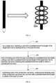
- FIG.3 is a structural schematic view of a wire provided in a third embodiment of the present disclosure which represents the present invention.
- cross-sectional areas of the first part and the third part of the wire are S, and a cross-sectional area of the second part is S/4; wherein the shape of the second part of the wire is elliptical and circular.
- the wires shown in FIG.2 and FIG.3 not only have no effect on use of the wires in the OLED device, but also enhance ductility of the wires, and the parts having been folded and curved of the wires are made into elliptical shape, the problem that the OLED device cannot normally work caused by wire fracture during folding can be avoided efficiently, thereby efficiently improving the using life of the OLED.
- the embodiments of the disclosure provide a wire for use in an organic light-emitting diode (OLED) device, wherein the wire comprises three parts, and a first part and a third part are located at both ends of the wire respectively and each of the first part and the third part is a single wire; a second part is located between the first part and the third part and is a composite wire, wherein the composite wire comprises at least two wires.
- OLED organic light-emitting diode
- the purpose of changing a wire width of a single wire is achieved, which not only has no influence on use of the wires in the OLED device, but also enhances ductility of the wires, thereby efficiently avoiding the occurrence of the problem that the OLED device cannot normally work caused by wire fracture during folding, and efficiently improving the using life of the OLED.
- FIG.4 is a schematic flowchart of a method for manufacturing a wire provided in an embodiment of the disclosure. The method may be as follows.
- Step 401 for a target wire, selecting a predetermined first length of the target wire from a starting end as a first part of the target wire.
- the predetermined length here may be set according to requirements for the OLED device and is not limited by the embodiment of the disclosure.
- Step 402 cutting the wire with a predetermined second length into at least two sub-wires satisfying the predetermined wire width may be made by adopting a manner of photo etching or other manners, and may also be made by employing a mask with a pattern of this wire to manufacture directly, which is not limited herein.
- Step 403 at finishing ends of the at least two sub-wires, combining the finishing ends of the at least two sub-wires into one wire to obtain a third part of the target wire.
- the solution of manufacturing a wire provided by the embodiment of the disclosure not only has no influence on use of the wires in the OLED device, but also enhance ductility of the wires, thereby efficiently avoiding the occurrence of the problem that the OLED device cannot normally work caused by wire fracture during folding, and efficiently improving the using efficiency of the OLED.
Landscapes
- Engineering & Computer Science (AREA)
- Microelectronics & Electronic Packaging (AREA)
- Electroluminescent Light Sources (AREA)
- Manufacturing & Machinery (AREA)
Claims (2)
- Draht zur Verwendung in einer organischen Leuchtdiode (OLED), wobei der Draht einen ersten Teil (11), einen zweiten Teil (12) und einen dritten Teil (13) umfasst, die miteinander verbunden sind, wobei sich der erste Teil (11) und der dritte Teil (13) jeweils an beiden Enden des Drahtes befinden, wobei sowohl der erste Teil (11) als auch der dritte Teil (13) ein einzelner Draht ist; undder zweite Teil (12) sich zwischen dem ersten Teil (11) und dem dritten Teil (13) befindet und ein Verbunddraht ist, wobei der Verbunddraht mindestens zwei Unterdrähte umfasst;dadurch gekennzeichnet, dass der Verbunddraht erste, zweite, dritte und vierte Unterdrähte umfasst, die auseinander laufen und konvergieren, um in einer Reihe mehrere Schleifen zu bilden, die miteinander verbunden sind und den ersten Teil mit dem dritten Teil verbinden, wobei jede Schleife umfassend den ersten und den vierten Unterdraht eine äußere Schleife mit einer elliptischen Form bildet, die eine innere Schleife mit einer kreisförmigen Form umgibt, die durch den zweiten und den dritten Unterdraht gebildet wird, wobei die Breite (S/4) jedes der ersten bis vierten Unterdrähte einem Viertel der Breite (s) des Drahtes am ersten Teil und am dritten Teil gleich ist, wobei die Drähte am ersten Teil und am dritten Teil die gleiche Breite (s) aufweisen,wobei die äußere Schleife den gleichen Durchmesser wie die innere Schleife in einer Längsrichtung des Drahtes aufweist und einen größeren Durchmesser als der Durchmesser der innere Schleife in einer Querrichtung senkrecht zu der Längsrichtung des Drahtes aufweist.
- Verfahren zur Herstellung eines Drahtes nach Anspruch 1, das Verfahren umfassend:Auswählen (401), für einen Zieldraht, einer vorbestimmten ersten Länge des Zieldrahtes ausgehend von einem Anfangsende als ein erster Teil (11) des Zieldrahtes;Schneiden (402) des Drahts mit einer vorbestimmten zweiten Länge in die ersten bis vierten Unterdrähte ausgehend von einem Abschlussende des ersten Teils (11) nach einem vorbestimmten Breite des Drahtes, wobei die Breite (S/4) jedes der ersten bis vierten Unterdrähte einem Viertel der Breite (s) des Drahts am ersten Teil (11) und am dritten Teil (13) gleich ist, um einen zweiten Teil (12) des Zieldrahts zu erhalten;Kombinieren (403), an den Abschlussenden des ersten bis vierten Unterdrahtes, der Abschlussenden des ersten bis vierten Teildrahtes zu einem Draht, um einen dritten Teil (13) des Zieldrahtes zu erhalten;wobei das Herstellen des Verbunddrahtes erste, zweite, dritte und vierte Unterdrähte umfasst, die auseinander laufen und konvergieren, um in einer Reihe mehrere Schleifen zu bilden, die miteinander verbunden sind und den ersten Teil mit dem dritten Teil verbinden, wobei jede Schleife umfassend die ersten und vierten Unterdrähte eine äußere Schleife mit einer elliptischen Form bildet, die eine innere Schleife mit einer kreisförmigen Form umgibt und die durch die zweiten und dritten Unterdrähte gebildet wird, wobei die Breite (S/4) jedes der ersten bis vierten Teildrähte einem Viertel der Breite des Drahtes am ersten Teil und am dritten Teil gleich ist, wobei die Drähte am ersten Teil und am dritten Teil die gleiche Breite aufweisen,wobei die äußere Schleife den gleichen Durchmesser wie die innere Schleife in einer Längsrichtung des Drahtes aufweist und einen größeren Durchmesser als der Durchmesser der innere Schleife in einer Querrichtung senkrecht zu der Längsrichtung des Drahtes aufweist.
Applications Claiming Priority (2)
| Application Number | Priority Date | Filing Date | Title |
|---|---|---|---|
| CN201610132850.6A CN107180808B (zh) | 2016-03-09 | 2016-03-09 | 一种导线及制作导线的方法 |
| PCT/CN2017/075070 WO2017152793A1 (zh) | 2016-03-09 | 2017-02-27 | 一种导线及制作导线的方法 |
Publications (3)
| Publication Number | Publication Date |
|---|---|
| EP3379571A1 EP3379571A1 (de) | 2018-09-26 |
| EP3379571A4 EP3379571A4 (de) | 2019-04-03 |
| EP3379571B1 true EP3379571B1 (de) | 2025-06-25 |
Family
ID=59789017
Family Applications (1)
| Application Number | Title | Priority Date | Filing Date |
|---|---|---|---|
| EP17762479.8A Active EP3379571B1 (de) | 2016-03-09 | 2017-02-27 | Draht und verfahren zur herstellung davon |
Country Status (7)
| Country | Link |
|---|---|
| US (1) | US10483130B2 (de) |
| EP (1) | EP3379571B1 (de) |
| JP (1) | JP6743157B2 (de) |
| KR (1) | KR102113782B1 (de) |
| CN (1) | CN107180808B (de) |
| TW (1) | TWI649907B (de) |
| WO (1) | WO2017152793A1 (de) |
Families Citing this family (3)
| Publication number | Priority date | Publication date | Assignee | Title |
|---|---|---|---|---|
| CN108320864A (zh) * | 2017-12-11 | 2018-07-24 | 芜湖航天特种电缆厂股份有限公司 | 机载设备线束组件及其生产工艺 |
| CN110942708B (zh) * | 2018-09-21 | 2021-08-27 | 元太科技工业股份有限公司 | 导电结构、线路设计及显示器 |
| JP2024010491A (ja) * | 2022-07-12 | 2024-01-24 | 株式会社ジャパンディスプレイ | ストレッチャブルアレイ基板 |
Citations (2)
| Publication number | Priority date | Publication date | Assignee | Title |
|---|---|---|---|---|
| US20140055702A1 (en) * | 2012-08-21 | 2014-02-27 | Young Bae Park | Displays with Bent Signal Lines |
| CN103730476A (zh) * | 2013-12-27 | 2014-04-16 | 京东方科技集团股份有限公司 | 阵列基板及显示装置 |
Family Cites Families (14)
| Publication number | Priority date | Publication date | Assignee | Title |
|---|---|---|---|---|
| JP5240827B2 (ja) * | 2008-04-15 | 2013-07-17 | Necカシオモバイルコミュニケーションズ株式会社 | フレキシブル配線基板、及び電子機器 |
| TWI394255B (zh) | 2008-10-14 | 2013-04-21 | 德州儀器公司 | 具有用以局限焊料毛細現象之溝槽式導線的半導體裝置 |
| JP5446790B2 (ja) * | 2009-12-02 | 2014-03-19 | セイコーエプソン株式会社 | 電気光学装置および電子機器 |
| KR20110125931A (ko) * | 2010-05-14 | 2011-11-22 | 삼성모바일디스플레이주식회사 | 유기 발광 표시 장치 및 그 제조 방법 |
| CN201788721U (zh) | 2010-08-04 | 2011-04-06 | 珠海格力电器股份有限公司 | Ito薄膜及具有该ito薄膜的透明触摸按键 |
| TWI453520B (zh) | 2011-08-16 | 2014-09-21 | Au Optronics Corp | 具有可修補導線的層疊結構之平面顯示面板及其修補方法 |
| US8933335B2 (en) | 2011-10-14 | 2015-01-13 | Varian Semiconductor Equipment Associates, Inc. | Current lead with a configuration to reduce heat load transfer in an alternating electrical current environment |
| CN103794733A (zh) * | 2012-10-31 | 2014-05-14 | 财团法人工业技术研究院 | 环境敏感电子元件封装体 |
| KR102097150B1 (ko) * | 2013-02-01 | 2020-04-03 | 엘지디스플레이 주식회사 | 플렉서블 디스플레이 기판, 플렉서블 유기 발광 표시 장치 및 플렉서블 유기 발광 표시 장치 제조 방법 |
| TWI790673B (zh) * | 2013-03-07 | 2023-01-21 | 日商半導體能源研究所股份有限公司 | 電子裝置 |
| US9544994B2 (en) * | 2014-08-30 | 2017-01-10 | Lg Display Co., Ltd. | Flexible display device with side crack protection structure and manufacturing method for the same |
| US9276055B1 (en) * | 2014-08-31 | 2016-03-01 | Lg Display Co., Ltd. | Display device with micro cover layer and manufacturing method for the same |
| CN105047676A (zh) * | 2015-09-06 | 2015-11-11 | 京东方科技集团股份有限公司 | 一种封装用柔性基板及封装体 |
| CN205406511U (zh) * | 2016-03-09 | 2016-07-27 | 昆山工研院新型平板显示技术中心有限公司 | 一种导线 |
-
2016
- 2016-03-09 CN CN201610132850.6A patent/CN107180808B/zh active Active
-
2017
- 2017-02-27 US US16/062,489 patent/US10483130B2/en active Active
- 2017-02-27 KR KR1020187023470A patent/KR102113782B1/ko active Active
- 2017-02-27 JP JP2018540022A patent/JP6743157B2/ja active Active
- 2017-02-27 WO PCT/CN2017/075070 patent/WO2017152793A1/zh not_active Ceased
- 2017-02-27 EP EP17762479.8A patent/EP3379571B1/de active Active
- 2017-03-03 TW TW106107097A patent/TWI649907B/zh active
Patent Citations (2)
| Publication number | Priority date | Publication date | Assignee | Title |
|---|---|---|---|---|
| US20140055702A1 (en) * | 2012-08-21 | 2014-02-27 | Young Bae Park | Displays with Bent Signal Lines |
| CN103730476A (zh) * | 2013-12-27 | 2014-04-16 | 京东方科技集团股份有限公司 | 阵列基板及显示装置 |
Also Published As
| Publication number | Publication date |
|---|---|
| EP3379571A1 (de) | 2018-09-26 |
| US10483130B2 (en) | 2019-11-19 |
| US20180366345A1 (en) | 2018-12-20 |
| KR20180105171A (ko) | 2018-09-27 |
| JP6743157B2 (ja) | 2020-08-19 |
| WO2017152793A1 (zh) | 2017-09-14 |
| CN107180808B (zh) | 2019-07-19 |
| KR102113782B1 (ko) | 2020-06-26 |
| JP2019506748A (ja) | 2019-03-07 |
| TWI649907B (zh) | 2019-02-01 |
| CN107180808A (zh) | 2017-09-19 |
| EP3379571A4 (de) | 2019-04-03 |
| TW201803180A (zh) | 2018-01-16 |
Similar Documents
| Publication | Publication Date | Title |
|---|---|---|
| KR102697421B1 (ko) | 표시 패널 | |
| KR102668243B1 (ko) | 보강된 부분을 갖는 배선을 포함하는 플렉서블 디스플레이 디바이스 및 이의 제조 방법 | |
| KR102739075B1 (ko) | 유기 발광 표시 장치 | |
| KR20240034720A (ko) | 디스플레이 장치 | |
| JP2023510055A (ja) | 支持プレート及び折り畳みディスプレイ | |
| KR102326122B1 (ko) | 터치 패널 및 이를 포함하는 화상 표시 장치 | |
| US11119536B2 (en) | Flexible electronic device and manufacturing method therefor | |
| CN110444575A (zh) | 可拉伸显示背板、可拉伸显示装置 | |
| TWI504969B (zh) | 顯示面板以及顯示裝置 | |
| US11226526B2 (en) | Wiring structure, display substrate and display device | |
| WO2021022583A1 (zh) | 柔性显示面板 | |
| US11114518B2 (en) | Wiring structure, display substrate and display device | |
| US10903444B2 (en) | OLED package substrate having a conductor attached to electrode on an array substrate | |
| KR102026829B1 (ko) | 칩 온 필름, 이를 갖는 플렉시블 디스플레이 장치, 및 그 제조 방법 | |
| KR102825873B1 (ko) | 디스플레이용 기판 및 이를 포함하는 디스플레이 장치 | |
| US12004392B2 (en) | Display panel and display device | |
| US11139355B2 (en) | Display panel having stress releasing structure and method for manufacturing same | |
| US10788944B2 (en) | Touch display panel, method of manufacturing touch display panel, and display apparatus | |
| EP3379571A1 (de) | Draht und verfahren zur herstellung davon | |
| WO2020107337A1 (zh) | 显示面板及显示装置 | |
| US10340295B2 (en) | Flexible display device and border unit thereof | |
| US9773961B1 (en) | Display panel | |
| TW202103528A (zh) | 軟硬複合電路板外框的應力消除結構 | |
| US20250003577A1 (en) | Light-emitting substrate, light-emitting apparatus and lighting apparatus | |
| CN107305904B (zh) | 显示面板 |
Legal Events
| Date | Code | Title | Description |
|---|---|---|---|
| STAA | Information on the status of an ep patent application or granted ep patent |
Free format text: STATUS: THE INTERNATIONAL PUBLICATION HAS BEEN MADE |
|
| PUAI | Public reference made under article 153(3) epc to a published international application that has entered the european phase |
Free format text: ORIGINAL CODE: 0009012 |
|
| STAA | Information on the status of an ep patent application or granted ep patent |
Free format text: STATUS: REQUEST FOR EXAMINATION WAS MADE |
|
| 17P | Request for examination filed |
Effective date: 20180619 |
|
| AK | Designated contracting states |
Kind code of ref document: A1 Designated state(s): AL AT BE BG CH CY CZ DE DK EE ES FI FR GB GR HR HU IE IS IT LI LT LU LV MC MK MT NL NO PL PT RO RS SE SI SK SM TR |
|
| AX | Request for extension of the european patent |
Extension state: BA ME |
|
| A4 | Supplementary search report drawn up and despatched |
Effective date: 20190306 |
|
| RIC1 | Information provided on ipc code assigned before grant |
Ipc: H01L 21/48 20060101ALI20190228BHEP Ipc: H01L 23/00 20060101ALI20190228BHEP Ipc: H01L 23/49 20060101AFI20190228BHEP Ipc: H01L 51/52 20060101ALI20190228BHEP Ipc: H01L 27/32 20060101ALI20190228BHEP |
|
| DAV | Request for validation of the european patent (deleted) | ||
| DAX | Request for extension of the european patent (deleted) | ||
| STAA | Information on the status of an ep patent application or granted ep patent |
Free format text: STATUS: EXAMINATION IS IN PROGRESS |
|
| 17Q | First examination report despatched |
Effective date: 20210506 |
|
| REG | Reference to a national code |
Ref country code: DE Ref legal event code: R079 Free format text: PREVIOUS MAIN CLASS: H01L0023490000 Ipc: H10K0059131000 Ref country code: DE Ref legal event code: R079 Ref document number: 602017090134 Country of ref document: DE Free format text: PREVIOUS MAIN CLASS: H01L0023490000 Ipc: H10K0059131000 |
|
| RIC1 | Information provided on ipc code assigned before grant |
Ipc: H01L 23/49 20060101ALI20230324BHEP Ipc: H01L 27/12 20060101ALI20230324BHEP Ipc: H10K 59/131 20230101AFI20230324BHEP |
|
| GRAP | Despatch of communication of intention to grant a patent |
Free format text: ORIGINAL CODE: EPIDOSNIGR1 |
|
| STAA | Information on the status of an ep patent application or granted ep patent |
Free format text: STATUS: GRANT OF PATENT IS INTENDED |
|
| RIC1 | Information provided on ipc code assigned before grant |
Ipc: H10K 102/00 20230101ALN20250115BHEP Ipc: H10D 86/60 20250101ALI20250115BHEP Ipc: H01L 23/49 20060101ALI20250115BHEP Ipc: H10D 86/40 20250101ALI20250115BHEP Ipc: H10K 59/131 20230101AFI20250115BHEP |
|
| INTG | Intention to grant announced |
Effective date: 20250204 |
|
| GRAS | Grant fee paid |
Free format text: ORIGINAL CODE: EPIDOSNIGR3 |
|
| GRAA | (expected) grant |
Free format text: ORIGINAL CODE: 0009210 |
|
| STAA | Information on the status of an ep patent application or granted ep patent |
Free format text: STATUS: THE PATENT HAS BEEN GRANTED |
|
| AK | Designated contracting states |
Kind code of ref document: B1 Designated state(s): AL AT BE BG CH CY CZ DE DK EE ES FI FR GB GR HR HU IE IS IT LI LT LU LV MC MK MT NL NO PL PT RO RS SE SI SK SM TR |
|
| REG | Reference to a national code |
Ref country code: GB Ref legal event code: FG4D |
|
| REG | Reference to a national code |
Ref country code: CH Ref legal event code: EP |
|
| REG | Reference to a national code |
Ref country code: CH Ref legal event code: EP |
|
| REG | Reference to a national code |
Ref country code: IE Ref legal event code: FG4D |
|
| REG | Reference to a national code |
Ref country code: DE Ref legal event code: R096 Ref document number: 602017090134 Country of ref document: DE |
|
| PG25 | Lapsed in a contracting state [announced via postgrant information from national office to epo] |
Ref country code: FI Free format text: LAPSE BECAUSE OF FAILURE TO SUBMIT A TRANSLATION OF THE DESCRIPTION OR TO PAY THE FEE WITHIN THE PRESCRIBED TIME-LIMIT Effective date: 20250625 |
|
| REG | Reference to a national code |
Ref country code: LT Ref legal event code: MG9D |
|
| PG25 | Lapsed in a contracting state [announced via postgrant information from national office to epo] |
Ref country code: GR Free format text: LAPSE BECAUSE OF FAILURE TO SUBMIT A TRANSLATION OF THE DESCRIPTION OR TO PAY THE FEE WITHIN THE PRESCRIBED TIME-LIMIT Effective date: 20250926 Ref country code: NO Free format text: LAPSE BECAUSE OF FAILURE TO SUBMIT A TRANSLATION OF THE DESCRIPTION OR TO PAY THE FEE WITHIN THE PRESCRIBED TIME-LIMIT Effective date: 20250925 |
|
| PG25 | Lapsed in a contracting state [announced via postgrant information from national office to epo] |
Ref country code: BG Free format text: LAPSE BECAUSE OF FAILURE TO SUBMIT A TRANSLATION OF THE DESCRIPTION OR TO PAY THE FEE WITHIN THE PRESCRIBED TIME-LIMIT Effective date: 20250625 |
|
| PG25 | Lapsed in a contracting state [announced via postgrant information from national office to epo] |
Ref country code: HR Free format text: LAPSE BECAUSE OF FAILURE TO SUBMIT A TRANSLATION OF THE DESCRIPTION OR TO PAY THE FEE WITHIN THE PRESCRIBED TIME-LIMIT Effective date: 20250625 |
|
| PG25 | Lapsed in a contracting state [announced via postgrant information from national office to epo] |
Ref country code: RS Free format text: LAPSE BECAUSE OF FAILURE TO SUBMIT A TRANSLATION OF THE DESCRIPTION OR TO PAY THE FEE WITHIN THE PRESCRIBED TIME-LIMIT Effective date: 20250925 |
|
| PG25 | Lapsed in a contracting state [announced via postgrant information from national office to epo] |
Ref country code: LV Free format text: LAPSE BECAUSE OF FAILURE TO SUBMIT A TRANSLATION OF THE DESCRIPTION OR TO PAY THE FEE WITHIN THE PRESCRIBED TIME-LIMIT Effective date: 20250625 |
|
| REG | Reference to a national code |
Ref country code: NL Ref legal event code: MP Effective date: 20250625 |
|
| PG25 | Lapsed in a contracting state [announced via postgrant information from national office to epo] |
Ref country code: NL Free format text: LAPSE BECAUSE OF FAILURE TO SUBMIT A TRANSLATION OF THE DESCRIPTION OR TO PAY THE FEE WITHIN THE PRESCRIBED TIME-LIMIT Effective date: 20250625 |
|
| PG25 | Lapsed in a contracting state [announced via postgrant information from national office to epo] |
Ref country code: PT Free format text: LAPSE BECAUSE OF FAILURE TO SUBMIT A TRANSLATION OF THE DESCRIPTION OR TO PAY THE FEE WITHIN THE PRESCRIBED TIME-LIMIT Effective date: 20251027 |
|
| REG | Reference to a national code |
Ref country code: AT Ref legal event code: MK05 Ref document number: 1808083 Country of ref document: AT Kind code of ref document: T Effective date: 20250625 |
|
| PG25 | Lapsed in a contracting state [announced via postgrant information from national office to epo] |
Ref country code: IS Free format text: LAPSE BECAUSE OF FAILURE TO SUBMIT A TRANSLATION OF THE DESCRIPTION OR TO PAY THE FEE WITHIN THE PRESCRIBED TIME-LIMIT Effective date: 20251025 |
|
| PG25 | Lapsed in a contracting state [announced via postgrant information from national office to epo] |
Ref country code: AT Free format text: LAPSE BECAUSE OF FAILURE TO SUBMIT A TRANSLATION OF THE DESCRIPTION OR TO PAY THE FEE WITHIN THE PRESCRIBED TIME-LIMIT Effective date: 20250625 Ref country code: SM Free format text: LAPSE BECAUSE OF FAILURE TO SUBMIT A TRANSLATION OF THE DESCRIPTION OR TO PAY THE FEE WITHIN THE PRESCRIBED TIME-LIMIT Effective date: 20250625 |
|
| PG25 | Lapsed in a contracting state [announced via postgrant information from national office to epo] |
Ref country code: CZ Free format text: LAPSE BECAUSE OF FAILURE TO SUBMIT A TRANSLATION OF THE DESCRIPTION OR TO PAY THE FEE WITHIN THE PRESCRIBED TIME-LIMIT Effective date: 20250625 |
|
| PG25 | Lapsed in a contracting state [announced via postgrant information from national office to epo] |
Ref country code: PL Free format text: LAPSE BECAUSE OF FAILURE TO SUBMIT A TRANSLATION OF THE DESCRIPTION OR TO PAY THE FEE WITHIN THE PRESCRIBED TIME-LIMIT Effective date: 20250625 |
|
| PG25 | Lapsed in a contracting state [announced via postgrant information from national office to epo] |
Ref country code: EE Free format text: LAPSE BECAUSE OF FAILURE TO SUBMIT A TRANSLATION OF THE DESCRIPTION OR TO PAY THE FEE WITHIN THE PRESCRIBED TIME-LIMIT Effective date: 20250625 |
|
| PG25 | Lapsed in a contracting state [announced via postgrant information from national office to epo] |
Ref country code: RO Free format text: LAPSE BECAUSE OF FAILURE TO SUBMIT A TRANSLATION OF THE DESCRIPTION OR TO PAY THE FEE WITHIN THE PRESCRIBED TIME-LIMIT Effective date: 20250625 Ref country code: SK Free format text: LAPSE BECAUSE OF FAILURE TO SUBMIT A TRANSLATION OF THE DESCRIPTION OR TO PAY THE FEE WITHIN THE PRESCRIBED TIME-LIMIT Effective date: 20250625 |
|
| PG25 | Lapsed in a contracting state [announced via postgrant information from national office to epo] |
Ref country code: ES Free format text: LAPSE BECAUSE OF FAILURE TO SUBMIT A TRANSLATION OF THE DESCRIPTION OR TO PAY THE FEE WITHIN THE PRESCRIBED TIME-LIMIT Effective date: 20250625 |
|
| PG25 | Lapsed in a contracting state [announced via postgrant information from national office to epo] |
Ref country code: DK Free format text: LAPSE BECAUSE OF FAILURE TO SUBMIT A TRANSLATION OF THE DESCRIPTION OR TO PAY THE FEE WITHIN THE PRESCRIBED TIME-LIMIT Effective date: 20250625 |
|
| PGFP | Annual fee paid to national office [announced via postgrant information from national office to epo] |
Ref country code: DE Payment date: 20260206 Year of fee payment: 10 |
|
| PG25 | Lapsed in a contracting state [announced via postgrant information from national office to epo] |
Ref country code: IT Free format text: LAPSE BECAUSE OF FAILURE TO SUBMIT A TRANSLATION OF THE DESCRIPTION OR TO PAY THE FEE WITHIN THE PRESCRIBED TIME-LIMIT Effective date: 20250625 |
|
| PLBE | No opposition filed within time limit |
Free format text: ORIGINAL CODE: 0009261 |
|
| STAA | Information on the status of an ep patent application or granted ep patent |
Free format text: STATUS: NO OPPOSITION FILED WITHIN TIME LIMIT |
|
| REG | Reference to a national code |
Ref country code: CH Ref legal event code: L10 Free format text: ST27 STATUS EVENT CODE: U-0-0-L10-L00 (AS PROVIDED BY THE NATIONAL OFFICE) Effective date: 20260507 |