EP3378089B1 - Electron beam source and method for operating the same - Google Patents
Electron beam source and method for operating the same Download PDFInfo
- Publication number
- EP3378089B1 EP3378089B1 EP16781437.5A EP16781437A EP3378089B1 EP 3378089 B1 EP3378089 B1 EP 3378089B1 EP 16781437 A EP16781437 A EP 16781437A EP 3378089 B1 EP3378089 B1 EP 3378089B1
- Authority
- EP
- European Patent Office
- Prior art keywords
- electron beam
- cathode
- beam source
- heating power
- predetermined
- Prior art date
- Legal status (The legal status is an assumption and is not a legal conclusion. Google has not performed a legal analysis and makes no representation as to the accuracy of the status listed.)
- Active
Links
- 238000010894 electron beam technology Methods 0.000 title claims description 144
- 238000000034 method Methods 0.000 title claims description 32
- 239000000843 powder Substances 0.000 claims description 66
- 238000010438 heat treatment Methods 0.000 claims description 63
- 238000003860 storage Methods 0.000 claims description 27
- 239000000463 material Substances 0.000 claims description 20
- 238000004590 computer program Methods 0.000 claims description 12
- 230000003247 decreasing effect Effects 0.000 claims description 6
- 238000000151 deposition Methods 0.000 claims description 3
- 238000001914 filtration Methods 0.000 claims 2
- 238000004519 manufacturing process Methods 0.000 description 16
- 238000004891 communication Methods 0.000 description 15
- 230000006870 function Effects 0.000 description 15
- 238000012545 processing Methods 0.000 description 13
- 239000000654 additive Substances 0.000 description 12
- 230000000996 additive effect Effects 0.000 description 12
- 238000010586 diagram Methods 0.000 description 12
- 230000008901 benefit Effects 0.000 description 8
- 238000009826 distribution Methods 0.000 description 8
- 230000000903 blocking effect Effects 0.000 description 6
- 239000000758 substrate Substances 0.000 description 6
- 230000004927 fusion Effects 0.000 description 5
- 230000015572 biosynthetic process Effects 0.000 description 4
- 230000008859 change Effects 0.000 description 4
- 238000005259 measurement Methods 0.000 description 4
- 230000001360 synchronised effect Effects 0.000 description 4
- 238000012986 modification Methods 0.000 description 3
- 230000004048 modification Effects 0.000 description 3
- 230000003287 optical effect Effects 0.000 description 3
- 239000007787 solid Substances 0.000 description 3
- 238000004846 x-ray emission Methods 0.000 description 3
- PXHVJJICTQNCMI-UHFFFAOYSA-N Nickel Chemical compound [Ni] PXHVJJICTQNCMI-UHFFFAOYSA-N 0.000 description 2
- 238000003491 array Methods 0.000 description 2
- 238000011109 contamination Methods 0.000 description 2
- 238000013461 design Methods 0.000 description 2
- 230000009977 dual effect Effects 0.000 description 2
- 238000010100 freeform fabrication Methods 0.000 description 2
- 229910052746 lanthanum Inorganic materials 0.000 description 2
- FZLIPJUXYLNCLC-UHFFFAOYSA-N lanthanum atom Chemical compound [La] FZLIPJUXYLNCLC-UHFFFAOYSA-N 0.000 description 2
- 230000033001 locomotion Effects 0.000 description 2
- 238000002844 melting Methods 0.000 description 2
- 230000008018 melting Effects 0.000 description 2
- 230000008569 process Effects 0.000 description 2
- 238000013515 script Methods 0.000 description 2
- 230000011664 signaling Effects 0.000 description 2
- IRLPACMLTUPBCL-KQYNXXCUSA-N 5'-adenylyl sulfate Chemical compound C1=NC=2C(N)=NC=NC=2N1[C@@H]1O[C@H](COP(O)(=O)OS(O)(=O)=O)[C@@H](O)[C@H]1O IRLPACMLTUPBCL-KQYNXXCUSA-N 0.000 description 1
- 229910000838 Al alloy Inorganic materials 0.000 description 1
- 229910000599 Cr alloy Inorganic materials 0.000 description 1
- 241000258963 Diplopoda Species 0.000 description 1
- 108010083687 Ion Pumps Proteins 0.000 description 1
- 229910001069 Ti alloy Inorganic materials 0.000 description 1
- RTAQQCXQSZGOHL-UHFFFAOYSA-N Titanium Chemical compound [Ti] RTAQQCXQSZGOHL-UHFFFAOYSA-N 0.000 description 1
- 229910052782 aluminium Inorganic materials 0.000 description 1
- XAGFODPZIPBFFR-UHFFFAOYSA-N aluminium Chemical compound [Al] XAGFODPZIPBFFR-UHFFFAOYSA-N 0.000 description 1
- 238000010420 art technique Methods 0.000 description 1
- 238000005452 bending Methods 0.000 description 1
- 230000009286 beneficial effect Effects 0.000 description 1
- 239000003990 capacitor Substances 0.000 description 1
- 239000000919 ceramic Substances 0.000 description 1
- 229920001940 conductive polymer Polymers 0.000 description 1
- 238000012937 correction Methods 0.000 description 1
- 238000013480 data collection Methods 0.000 description 1
- 238000013500 data storage Methods 0.000 description 1
- 230000000694 effects Effects 0.000 description 1
- 238000005516 engineering process Methods 0.000 description 1
- 238000007667 floating Methods 0.000 description 1
- 238000007499 fusion processing Methods 0.000 description 1
- 238000013507 mapping Methods 0.000 description 1
- 229910052751 metal Inorganic materials 0.000 description 1
- 239000002184 metal Substances 0.000 description 1
- 229910001092 metal group alloy Inorganic materials 0.000 description 1
- 150000002739 metals Chemical class 0.000 description 1
- 238000010295 mobile communication Methods 0.000 description 1
- 230000006855 networking Effects 0.000 description 1
- 229910052759 nickel Inorganic materials 0.000 description 1
- 229910052710 silicon Inorganic materials 0.000 description 1
- 239000010703 silicon Substances 0.000 description 1
- 238000005245 sintering Methods 0.000 description 1
- 239000010935 stainless steel Substances 0.000 description 1
- 229910001220 stainless steel Inorganic materials 0.000 description 1
- 230000003068 static effect Effects 0.000 description 1
- 229910000601 superalloy Inorganic materials 0.000 description 1
- -1 titanium Chemical class 0.000 description 1
- 239000010936 titanium Substances 0.000 description 1
- 229910052719 titanium Inorganic materials 0.000 description 1
- 238000012546 transfer Methods 0.000 description 1
Images

Classifications
-
- H—ELECTRICITY
- H01—ELECTRIC ELEMENTS
- H01J—ELECTRIC DISCHARGE TUBES OR DISCHARGE LAMPS
- H01J37/00—Discharge tubes with provision for introducing objects or material to be exposed to the discharge, e.g. for the purpose of examination or processing thereof
- H01J37/02—Details
- H01J37/04—Arrangements of electrodes and associated parts for generating or controlling the discharge, e.g. electron-optical arrangement or ion-optical arrangement
- H01J37/06—Electron sources; Electron guns
- H01J37/07—Eliminating deleterious effects due to thermal effects or electric or magnetic fields
-
- B—PERFORMING OPERATIONS; TRANSPORTING
- B22—CASTING; POWDER METALLURGY
- B22F—WORKING METALLIC POWDER; MANUFACTURE OF ARTICLES FROM METALLIC POWDER; MAKING METALLIC POWDER; APPARATUS OR DEVICES SPECIALLY ADAPTED FOR METALLIC POWDER
- B22F10/00—Additive manufacturing of workpieces or articles from metallic powder
- B22F10/20—Direct sintering or melting
- B22F10/28—Powder bed fusion, e.g. selective laser melting [SLM] or electron beam melting [EBM]
-
- B—PERFORMING OPERATIONS; TRANSPORTING
- B22—CASTING; POWDER METALLURGY
- B22F—WORKING METALLIC POWDER; MANUFACTURE OF ARTICLES FROM METALLIC POWDER; MAKING METALLIC POWDER; APPARATUS OR DEVICES SPECIALLY ADAPTED FOR METALLIC POWDER
- B22F3/00—Manufacture of workpieces or articles from metallic powder characterised by the manner of compacting or sintering; Apparatus specially adapted therefor ; Presses and furnaces
- B22F3/10—Sintering only
- B22F3/1017—Multiple heating or additional steps
-
- B—PERFORMING OPERATIONS; TRANSPORTING
- B23—MACHINE TOOLS; METAL-WORKING NOT OTHERWISE PROVIDED FOR
- B23K—SOLDERING OR UNSOLDERING; WELDING; CLADDING OR PLATING BY SOLDERING OR WELDING; CUTTING BY APPLYING HEAT LOCALLY, e.g. FLAME CUTTING; WORKING BY LASER BEAM
- B23K15/00—Electron-beam welding or cutting
- B23K15/0046—Welding
- B23K15/0086—Welding welding for purposes other than joining, e.g. built-up welding
-
- B—PERFORMING OPERATIONS; TRANSPORTING
- B23—MACHINE TOOLS; METAL-WORKING NOT OTHERWISE PROVIDED FOR
- B23K—SOLDERING OR UNSOLDERING; WELDING; CLADDING OR PLATING BY SOLDERING OR WELDING; CUTTING BY APPLYING HEAT LOCALLY, e.g. FLAME CUTTING; WORKING BY LASER BEAM
- B23K15/00—Electron-beam welding or cutting
- B23K15/02—Control circuits therefor
-
- B—PERFORMING OPERATIONS; TRANSPORTING
- B29—WORKING OF PLASTICS; WORKING OF SUBSTANCES IN A PLASTIC STATE IN GENERAL
- B29C—SHAPING OR JOINING OF PLASTICS; SHAPING OF MATERIAL IN A PLASTIC STATE, NOT OTHERWISE PROVIDED FOR; AFTER-TREATMENT OF THE SHAPED PRODUCTS, e.g. REPAIRING
- B29C64/00—Additive manufacturing, i.e. manufacturing of three-dimensional [3D] objects by additive deposition, additive agglomeration or additive layering, e.g. by 3D printing, stereolithography or selective laser sintering
- B29C64/10—Processes of additive manufacturing
- B29C64/141—Processes of additive manufacturing using only solid materials
- B29C64/153—Processes of additive manufacturing using only solid materials using layers of powder being selectively joined, e.g. by selective laser sintering or melting
-
- B—PERFORMING OPERATIONS; TRANSPORTING
- B29—WORKING OF PLASTICS; WORKING OF SUBSTANCES IN A PLASTIC STATE IN GENERAL
- B29C—SHAPING OR JOINING OF PLASTICS; SHAPING OF MATERIAL IN A PLASTIC STATE, NOT OTHERWISE PROVIDED FOR; AFTER-TREATMENT OF THE SHAPED PRODUCTS, e.g. REPAIRING
- B29C64/00—Additive manufacturing, i.e. manufacturing of three-dimensional [3D] objects by additive deposition, additive agglomeration or additive layering, e.g. by 3D printing, stereolithography or selective laser sintering
- B29C64/30—Auxiliary operations or equipment
- B29C64/386—Data acquisition or data processing for additive manufacturing
- B29C64/393—Data acquisition or data processing for additive manufacturing for controlling or regulating additive manufacturing processes
-
- B—PERFORMING OPERATIONS; TRANSPORTING
- B33—ADDITIVE MANUFACTURING TECHNOLOGY
- B33Y—ADDITIVE MANUFACTURING, i.e. MANUFACTURING OF THREE-DIMENSIONAL [3-D] OBJECTS BY ADDITIVE DEPOSITION, ADDITIVE AGGLOMERATION OR ADDITIVE LAYERING, e.g. BY 3-D PRINTING, STEREOLITHOGRAPHY OR SELECTIVE LASER SINTERING
- B33Y10/00—Processes of additive manufacturing
-
- B—PERFORMING OPERATIONS; TRANSPORTING
- B33—ADDITIVE MANUFACTURING TECHNOLOGY
- B33Y—ADDITIVE MANUFACTURING, i.e. MANUFACTURING OF THREE-DIMENSIONAL [3-D] OBJECTS BY ADDITIVE DEPOSITION, ADDITIVE AGGLOMERATION OR ADDITIVE LAYERING, e.g. BY 3-D PRINTING, STEREOLITHOGRAPHY OR SELECTIVE LASER SINTERING
- B33Y30/00—Apparatus for additive manufacturing; Details thereof or accessories therefor
-
- B—PERFORMING OPERATIONS; TRANSPORTING
- B33—ADDITIVE MANUFACTURING TECHNOLOGY
- B33Y—ADDITIVE MANUFACTURING, i.e. MANUFACTURING OF THREE-DIMENSIONAL [3-D] OBJECTS BY ADDITIVE DEPOSITION, ADDITIVE AGGLOMERATION OR ADDITIVE LAYERING, e.g. BY 3-D PRINTING, STEREOLITHOGRAPHY OR SELECTIVE LASER SINTERING
- B33Y50/00—Data acquisition or data processing for additive manufacturing
- B33Y50/02—Data acquisition or data processing for additive manufacturing for controlling or regulating additive manufacturing processes
-
- H—ELECTRICITY
- H01—ELECTRIC ELEMENTS
- H01J—ELECTRIC DISCHARGE TUBES OR DISCHARGE LAMPS
- H01J37/00—Discharge tubes with provision for introducing objects or material to be exposed to the discharge, e.g. for the purpose of examination or processing thereof
- H01J37/02—Details
- H01J37/04—Arrangements of electrodes and associated parts for generating or controlling the discharge, e.g. electron-optical arrangement or ion-optical arrangement
- H01J37/06—Electron sources; Electron guns
- H01J37/075—Electron guns using thermionic emission from cathodes heated by particle bombardment or by irradiation, e.g. by laser
-
- H—ELECTRICITY
- H01—ELECTRIC ELEMENTS
- H01J—ELECTRIC DISCHARGE TUBES OR DISCHARGE LAMPS
- H01J37/00—Discharge tubes with provision for introducing objects or material to be exposed to the discharge, e.g. for the purpose of examination or processing thereof
- H01J37/02—Details
- H01J37/24—Circuit arrangements not adapted to a particular application of the tube and not otherwise provided for
- H01J37/242—Filament heating power supply or regulation circuits
-
- B—PERFORMING OPERATIONS; TRANSPORTING
- B22—CASTING; POWDER METALLURGY
- B22F—WORKING METALLIC POWDER; MANUFACTURE OF ARTICLES FROM METALLIC POWDER; MAKING METALLIC POWDER; APPARATUS OR DEVICES SPECIALLY ADAPTED FOR METALLIC POWDER
- B22F10/00—Additive manufacturing of workpieces or articles from metallic powder
- B22F10/30—Process control
- B22F10/32—Process control of the atmosphere, e.g. composition or pressure in a building chamber
-
- B—PERFORMING OPERATIONS; TRANSPORTING
- B22—CASTING; POWDER METALLURGY
- B22F—WORKING METALLIC POWDER; MANUFACTURE OF ARTICLES FROM METALLIC POWDER; MAKING METALLIC POWDER; APPARATUS OR DEVICES SPECIALLY ADAPTED FOR METALLIC POWDER
- B22F10/00—Additive manufacturing of workpieces or articles from metallic powder
- B22F10/30—Process control
- B22F10/36—Process control of energy beam parameters
- B22F10/364—Process control of energy beam parameters for post-heating, e.g. remelting
-
- B—PERFORMING OPERATIONS; TRANSPORTING
- B22—CASTING; POWDER METALLURGY
- B22F—WORKING METALLIC POWDER; MANUFACTURE OF ARTICLES FROM METALLIC POWDER; MAKING METALLIC POWDER; APPARATUS OR DEVICES SPECIALLY ADAPTED FOR METALLIC POWDER
- B22F12/00—Apparatus or devices specially adapted for additive manufacturing; Auxiliary means for additive manufacturing; Combinations of additive manufacturing apparatus or devices with other processing apparatus or devices
- B22F12/10—Auxiliary heating means
- B22F12/13—Auxiliary heating means to preheat the material
-
- B—PERFORMING OPERATIONS; TRANSPORTING
- B22—CASTING; POWDER METALLURGY
- B22F—WORKING METALLIC POWDER; MANUFACTURE OF ARTICLES FROM METALLIC POWDER; MAKING METALLIC POWDER; APPARATUS OR DEVICES SPECIALLY ADAPTED FOR METALLIC POWDER
- B22F12/00—Apparatus or devices specially adapted for additive manufacturing; Auxiliary means for additive manufacturing; Combinations of additive manufacturing apparatus or devices with other processing apparatus or devices
- B22F12/10—Auxiliary heating means
- B22F12/17—Auxiliary heating means to heat the build chamber or platform
-
- B—PERFORMING OPERATIONS; TRANSPORTING
- B22—CASTING; POWDER METALLURGY
- B22F—WORKING METALLIC POWDER; MANUFACTURE OF ARTICLES FROM METALLIC POWDER; MAKING METALLIC POWDER; APPARATUS OR DEVICES SPECIALLY ADAPTED FOR METALLIC POWDER
- B22F12/00—Apparatus or devices specially adapted for additive manufacturing; Auxiliary means for additive manufacturing; Combinations of additive manufacturing apparatus or devices with other processing apparatus or devices
- B22F12/40—Radiation means
- B22F12/49—Scanners
-
- B—PERFORMING OPERATIONS; TRANSPORTING
- B22—CASTING; POWDER METALLURGY
- B22F—WORKING METALLIC POWDER; MANUFACTURE OF ARTICLES FROM METALLIC POWDER; MAKING METALLIC POWDER; APPARATUS OR DEVICES SPECIALLY ADAPTED FOR METALLIC POWDER
- B22F12/00—Apparatus or devices specially adapted for additive manufacturing; Auxiliary means for additive manufacturing; Combinations of additive manufacturing apparatus or devices with other processing apparatus or devices
- B22F12/50—Means for feeding of material, e.g. heads
- B22F12/52—Hoppers
-
- B—PERFORMING OPERATIONS; TRANSPORTING
- B22—CASTING; POWDER METALLURGY
- B22F—WORKING METALLIC POWDER; MANUFACTURE OF ARTICLES FROM METALLIC POWDER; MAKING METALLIC POWDER; APPARATUS OR DEVICES SPECIALLY ADAPTED FOR METALLIC POWDER
- B22F12/00—Apparatus or devices specially adapted for additive manufacturing; Auxiliary means for additive manufacturing; Combinations of additive manufacturing apparatus or devices with other processing apparatus or devices
- B22F12/50—Means for feeding of material, e.g. heads
- B22F12/55—Two or more means for feeding material
-
- B—PERFORMING OPERATIONS; TRANSPORTING
- B22—CASTING; POWDER METALLURGY
- B22F—WORKING METALLIC POWDER; MANUFACTURE OF ARTICLES FROM METALLIC POWDER; MAKING METALLIC POWDER; APPARATUS OR DEVICES SPECIALLY ADAPTED FOR METALLIC POWDER
- B22F2998/00—Supplementary information concerning processes or compositions relating to powder metallurgy
- B22F2998/10—Processes characterised by the sequence of their steps
-
- B—PERFORMING OPERATIONS; TRANSPORTING
- B22—CASTING; POWDER METALLURGY
- B22F—WORKING METALLIC POWDER; MANUFACTURE OF ARTICLES FROM METALLIC POWDER; MAKING METALLIC POWDER; APPARATUS OR DEVICES SPECIALLY ADAPTED FOR METALLIC POWDER
- B22F2999/00—Aspects linked to processes or compositions used in powder metallurgy
-
- H—ELECTRICITY
- H01—ELECTRIC ELEMENTS
- H01J—ELECTRIC DISCHARGE TUBES OR DISCHARGE LAMPS
- H01J2237/00—Discharge tubes exposing object to beam, e.g. for analysis treatment, etching, imaging
- H01J2237/06—Sources
- H01J2237/063—Electron sources
- H01J2237/06308—Thermionic sources
-
- H—ELECTRICITY
- H01—ELECTRIC ELEMENTS
- H01J—ELECTRIC DISCHARGE TUBES OR DISCHARGE LAMPS
- H01J2237/00—Discharge tubes exposing object to beam, e.g. for analysis treatment, etching, imaging
- H01J2237/06—Sources
- H01J2237/065—Source emittance characteristics
-
- Y—GENERAL TAGGING OF NEW TECHNOLOGICAL DEVELOPMENTS; GENERAL TAGGING OF CROSS-SECTIONAL TECHNOLOGIES SPANNING OVER SEVERAL SECTIONS OF THE IPC; TECHNICAL SUBJECTS COVERED BY FORMER USPC CROSS-REFERENCE ART COLLECTIONS [XRACs] AND DIGESTS
- Y02—TECHNOLOGIES OR APPLICATIONS FOR MITIGATION OR ADAPTATION AGAINST CLIMATE CHANGE
- Y02P—CLIMATE CHANGE MITIGATION TECHNOLOGIES IN THE PRODUCTION OR PROCESSING OF GOODS
- Y02P10/00—Technologies related to metal processing
- Y02P10/25—Process efficiency
Definitions
- the present invention relates to an electron beam source and a method for prolonging the lifetime of an electron beam source.
- Freeform fabrication or additive manufacturing is a method for forming three-dimensional articles through successive fusion of chosen parts of powder layers applied to a worktable.
- An additive manufacturing apparatus may comprise a work table on which the three-dimensional article is to be formed, a powder dispenser or powder distributor, arranged to lay down a thin layer of powder on the work table for the formation of a powder bed, a high energy beam for delivering energy to the powder whereby fusion of the powder takes place, elements for control of the energy given off by the energy beam over the powder bed for the formation of a cross section of the three-dimensional article through fusion of parts of the powder bed, and a controlling computer, in which information is stored concerning consecutive cross sections of the three-dimensional article.
- a three-dimensional article is formed through consecutive fusions of consecutively formed cross sections of powder layers, successively laid down by the powder dispenser. Reference is made to, for example, to EP 2 911 181 A1 .
- the life time of the cathode element is one thing which constantly requires service in form of exchange when being worn out. It is desirable to extend the lifetime of the cathode element.
- Today the electron beam source settings is mainly performed manually which may introduce settings which reduces the lifetime from the very outset and/or after a period of time when the performance of the cathode element has changed. Reference is made to, for example, JP 2005 024343 A .
- An object of various embodiments of the invention is to provide a method which prolongs the lifetime of an electron beam source.
- the above-mentioned object is achieved by the features recited in the claims provided herein.
- a method for prolonging lifetime of at least one electron beam source comprising the steps of: providing the at least one electron beam source emitting an electron beam, where the electron beam source comprises a cathode, an anode, and a grid between the cathode and anode; setting an electron beam current, a cathode heating power, a grid potential Ug and a cathode potential Uc to predetermined start values, reducing the cathode heating power with a predetermined value and decreasing a Uc - Ug potential difference for maintaining the predetermined electron beam current, detecting an X-ray signal emanating from the electron beam source with at least one X-ray detector, repeating step c and d (the last two steps) until the detected X-ray signal is above a predetermined value, and increasing the cathode heating power by a predetermined safety value from a threshold heating power value which resulted in x-ray signals, emanating from the electron beam source,
- An exemplary advantage of various embodiments of the present invention is that it gives much better control of the heating power of the cathode element than prior art technique. Another advantage is that it is possible to adjust the heating power depending on the actual hours the cathode element has been used. Yet another advantage of the present invention is that the heating power may be set optimally individually for different additive manufacturing machines.
- the start value of the electron beam current is between 20-50mA.
- An exemplary advantage of at least these embodiments is that the method works for any suitable electron beam current which may be sued during additive manufacturing.
- the present invention further comprising the step of arranging the X-ray detector in the electron beam source.
- An exemplary advantage of at least these embodiments is that the detector is arranged for receiving x-rays emanating from the electron beam source only. In case of any background x-ray signal emanating from any other place in the additive manufacturing machine such X-rays may be filtered away easily.
- three-dimensional structures and the like as used herein refer generally to intended or actually fabricated three-dimensional configurations (e.g., of structural material or materials) that are intended to be used for a particular purpose. Such structures, etc. may, for example, be designed with the aid of a three-dimensional CAD system.
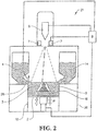
- Figure 2 depicts an embodiment of a freeform fabrication or additive manufacturing apparatus 21 in which the inventive method according to the present invention may be implemented.
- the apparatus 21 comprising an electron beam gun 6; deflection coils 7; two powder hoppers 4, 14; a build platform 2; a build tank 10; a powder distributor 28; a powder bed 5; and a vacuum chamber 20.
- the vacuum chamber 20 is capable of maintaining a vacuum environment via a vacuum system, which system may comprise a turbo molecular pump, a scroll pump, an ion pump and one or more valves which are well known to a skilled person in the art and therefore need no further explanation in this context.
- the vacuum system is controlled by a control unit 8.
- the electron beam gun 6 is generating an electron beam which is used for pre heating of the powder, melting or fusing together powder material provided on the build platform 2 or post heat treatment of the already fused powder material. At least a portion of the electron beam gun 6 may be provided in the vacuum chamber 20.
- the control unit 8 may be used for controlling and managing the electron beam emitted from the electron beam gun 6. At least one focusing coil (not shown), at least one deflection coil 7, an optional coil for astigmatic correction (not shown) and an electron beam power supply (not shown) may be electrically connected to the control unit 8.
- the electron beam gun 6 may generate a focusable electron beam with an accelerating voltage of about 15-60kV and with a beam power in the range of 3-10kW.
- the pressure in the vacuum chamber may be 10 -3 mbar or lower when building the three-dimensional article by fusing the powder layer by layer with the energy beam.
- the powder hoppers 4, 14 comprise the powder material to be provided on the build platform 2 in the build tank 10.
- the powder material may for instance be pure metals or metal alloys such as titanium, titanium alloys, aluminum, aluminum alloys, stainless steel, Co-Cr alloys, nickel based super alloys, etc.
- the powder distributor 28 is arranged to lay down a thin layer of the powder material on the build platform 2.
- the build platform 2 will be lowered successively in relation to a fixed point in the vacuum chamber.
- the build platform 2 is in one embodiment of the invention arranged movably in vertical direction, i.e., in the direction indicated by arrow P. This means that the build platform 2 starts in an initial position, in which a first powder material layer of necessary thickness has been laid down.
- Means for lowering the build platform 2 may for instance be through a servo engine equipped with a gear, adjusting screws, etc.
- the servo engine may be connected to the control unit 8.
- An electron beam may be directed over the build platform 2 causing the first powder layer to fuse in selected locations to form a first cross section of the three-dimensional article 3.
- the beam is directed over the build platform 2 from instructions given by the control unit 8.
- instructions for how to control the electron beam for each layer of the three-dimensional article is stored.
- the first layer of the three dimensional article 3 may be built on the build platform 2, which may be removable, in the powder bed 5 or on an optional start plate 16.
- the start plate 16 may be arranged directly on the build platform 2 or on top of a powder bed 5 which is provided on the build platform 2.
- a second powder layer is provided on the build platform 2.
- the thickness of the second layer may be determined by the distance the build platform is lowered in relation to the position where the first layer was built.
- the second powder layer is in various embodiments distributed according to the same manner as the previous layer.
- a first layer may be provided via a first powder distributor 28, a second layer may be provided by another powder distributor.
- the design of the powder distributor is automatically changed according to instructions from the control unit 8.
- a powder distributor 28 in the form of a single rake system, i.e., where one rake is catching powder fallen down from both a left powder hopper 4 and a right powder hopper 14, the rake as such can change design.
- the energy beam is directed over the work table causing the second powder layer to fuse in selected locations to form a second cross section of the three-dimensional article.
- Fused portions in the second layer may be bonded to fused portions of the first layer.
- the fused portions in the first and second layer may be melted together by melting not only the powder in the uppermost layer but also remelting at least a fraction of a thickness of a layer directly below the uppermost layer.
- the charge distribution density depends on the following parameters: beam current, electron velocity (which is given by the accelerating voltage), beam scanning velocity, powder material and electrical conductivity of the powder, i.e., mainly the electrical conductivity between the powder grains.
- beam current electron velocity (which is given by the accelerating voltage)
- electron scanning velocity powder material
- electrical conductivity of the powder i.e., mainly the electrical conductivity between the powder grains.
- the latter is in turn a function of several parameters, such as the non-limiting examples of temperature, degree of sintering and powder grain size/size distribution.
- the electrical conductivity of the powder can gradually be increased by increasing the temperature of the powder.
- a powder that has a high temperature obtains a considerably higher conductivity which results in a lower density of the charge distribution since the charges quickly can diffuse over a large region. This effect is enhanced if the powder is allowed to be slightly sintered during a pre-heating process.
- the powder can be fused together, i.e., melted or fully sintered, with predetermined values of the beam current and beam scanning velocity.
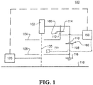
- FIG. 1 depicts, in a schematic view, an exemplary embodiment of an electron beam source in which the inventive method may be implemented.
- the electron beam source 100 comprises a cathode 102, a grid 104 and an anode 106. Electrons emitted at the cathode 102 being on negative potential are accelerated towards the anode 106 and finally a target surface 118.
- a grid 104 is set at a predetermined distance from the cathode 102.
- the cathode 102 may be provided with a heating power which may cause the cathode to heat up, where upon the cathode 102 releases electrons by thermionic emission.
- the heating power is typically around 5W for a lanthanum hexaboride (LaB6) cathode element.
- LaB6 lanthanum hexaboride
- An accelerator voltage 160 is provided between the cathode and the anode 106.
- the accelerator voltage 160 causes the emitted electrons from the cathode 102 to accelerate towards the anode 106 thus establishing an electron beam 120.
- the electron beam 120 may impinge on a substrate surface 118, which may be a powder layer in an additive manufacturing process.
- a substrate surface 118 which may be a powder layer in an additive manufacturing process.
- there may further be arranged at least one focusing coil and at least one deflection coil.
- the grid 104 is provided between the cathode 102 and the anode 106.
- the grid 104 may be arranged as a plate having an aperture.
- the aperture may be aligned with the cathode 102.
- the size of the aperture in the grid 104 may correspond to a cross section of the electron beam 120 at the position of the grid 104.
- a grid voltage 180 may be provided between the grid 104 and the cathode 102 and may be adjusted between a negative blocking voltage and a full power voltage and thereby adjusting an electron beam current between 0 - maximum electron beam current.
- the cathode 102 may be provided with a negative potential Uc of -20kV to -100kY.
- a first connection point 110 of the accelerator voltage 160 and a first connection point 114 of the grid voltage 180 may be fixed to the same potential of -20kV to -100kV.
- a second connection point 108 of the accelerator voltage 160 may be provided with ground potential.
- a second connection point 112 of the grid voltage 180 may be varied between the negative blocking voltage and the full power voltage.
- a second control unit 150 may be controlling the negative potential Ug on the second connection point 112 of the grid voltage in order to adjust the electron beam current to a desired value.
- the second control unit 150 may be a physically separate control unit in connection with the control unit 8 or fully integrated in the control unit 8.
- the target surface 118 may be set to ground potential or a positive potential.
- the electron beam source 100 may also comprise means 170 for detecting the actual electron beam current.
- An example means for detecting the electron beam current on the target surface may be to detect the actual loading of the high voltage source providing the accelerator voltage 160, indicated by box 170 in Figure 1 . This may be done by simply measuring the electron beam passing between the first and second connection points 110 and 108 respectively. If the cathode is provided with a fixed negative voltage of -60kV the negative blocking voltage may be around -61kV, i.e., the second connection point 112 of the grid voltage is set at -61kV and the first connection point 114 is set to -60kV, for blocking the electrons by the grid 104.
- the electron beam current may vary from 0mA - maximum electron beam current which may be 25mA for a predetermined size and shape of the cathode and a predetermined size and shape of the aperture in the grid 104.
- Other accelerator voltages and/or other size, shape and emissivity of the cathode and/or other size and shape of the aperture in the grid may affect the maximum electron beam current to be higher or lower than the exemplified 25mA.
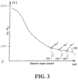
- Figure 3 depicts the grid potential - cathode potential as a function of electron beam current for different emissivity of a filament.
- the grid voltage 180 is at a sufficiently high negative potential, i.e., the potential on connection point 112 is provided with a sufficient negative potential (negative blocking potential) compared to the negative potential on connection point 114, the electrons emanating from the cathode 102 will be blocked (repelled) by the negative potential on the grid 104 resulting in no electrons passing through the aperture in the grid 104.
- the potential difference between the cathode 102 and grid 104 is decreasing the electron beam current is increasing, i.e., we are moving to the right in the graph in Figure 3 .
- Uc represents the cathode potential and U G represents the grid potential.
- a cathode 102 at different temperatures may emanate different amounts of electrons.
- FIG 3 it is illustrated 4 different graphs 310, 320, 330 and 340.
- a first graph 310 may represent a cathode at a first temperature.
- a second graph 320 may represent a cathode at a second temperature.
- a third graph 330 may represent a cathode at a third temperature.
- a fourth graph 310 may represent a cathode at a fourth temperature.
- the first temperature ⁇ the second temperature ⁇ the third temperature ⁇ the fourth temperature.
- the temperature of the cathode may not be the only parameter that affects the numbers of emanating electrons.
- FIG. 3 An unused cathode may be represented by graph 340. The more the cathode 102 is used the last portion of the graph is shifted to the left. A combination of a change in temperature of the cathode and the degree of use may also be represented by the different graphs in Figure 3 , i.e., for relatively cold cathodes and well used the last portion will be shifted to the left and for a relatively hot and new cathode the graph will be shifted to the right.
- the graph in Figure 3 may be defined by applying a predetermined number of different Uc - Ug potentials and measuring the resulting electron beam current for the Uc - Ug potentials.
- the graph may be approximated by a mathematical expression, for instance a polynomial which is fitted to the graph.
- the invention is how to prolong the life time of the cathode element. If providing an excessive amount of heating power the lifetime of the cathode element is heavily reduced.
- the invention is about how to determine the lowest acceptable heating power of the cathode element without affecting the electron beam current range of the electron beam source. If looking at figure 3 , one needs to determine when the Uc-Ug starts to change abruptly for a specific electron beam current denoted by 310', 320', 330'. Since x-rays are created instantly as the electron beam hits the internal structure of the electron beam source it is a very good measure of an electron beam path within the electron beam source which is not correct. A very small amount of the electron beam is needed for creating a detectable X-ray signal.
- the internal structure of the electron beam source may be a grid plate, an electron tube arranged as a last/final component in the electron beam source, or any component in the electron beam source.
- the idea is to use an X-ray detector 190 provided in the electron beam source for detecting X-rays emanating from the electron beam source. Obviously x-rays are created when the electron beam is hitting the substrate 118 but the X-ray detector is out of sight from the x-rays and/or the x-rays emanating from the substrate will only create a background X-ray noise which is known and can be eliminated from the detected x-ray signal in detector 190.
- the electron beam source is set to a predetermined electron beam current using a predetermined cathode hating power together with a predetermined grid potential Ug and a predetermined cathode potential Uc.
- the cathode potential may be kept constant throughout the determination of the heating power of the cathode element.
- An X-ray signal is detected by the X-ray detector 190. If the X-ray signal is below a predetermined value the cathode heating power may be reduced by a predetermined heating power step. In order to keep the electron beam current constant when the heating power is reduced the Uc-Ug potential needs to be decreased.
- the heating power step may for instance be 0.05W.
- the X-ray detector is again detecting the X-ray signal.
- the X-ray signal is still below the predetermined value a further decrease in heating power is performed together with a new decrease in Uc-Ug potential and yet a new X-ray measurement is made.
- the X-ray signal is above a predetermined value, it means that the heating power is too low for creating a predetermined electron beam current.
- the Uc-Ug potential is also reduced in order to maintain the constant electron beam current.
- the Uc-Ug potential will be so low that electron emissions from the cathode element will hit internal elements within the electron beam source and thereby create X-ray emission.
- a relatively low grid potential from a relatively "cold" cathode element will result in electron emission in direction not only towards the substrate but also electron emission which will hit internal elements within the electron beam source.
- X-rays detected by the detector 190 are mainly emanating from the electron beam source as such. This means that when the electron beam hits the internal structure of the electron beam source before the electron beam is leaving the electron beam source.
- One or a plurality of detectors may be used.
- a detector may be arranged for receiving x-rays signals from a particular area of the electron beam source. If the complete electron beam source is to be detected more than one x-ray detector may be needed.
- the risk of hitting the internal structure with the complete electron beam is reduced and/or eliminated if the starting value of the heating power is chosen in a safe interval where one knows by experience that no x-rays should be detected.
- a Uc-Ug of about 300 V or higher and a heating power above 5w may be a good starting point for a lanthanum hexaboride cathode element. If the heating power is reduced by predetermined steps closely enough spaced apart the method will prohibit full impact of the electron beam into the internal structure of the electron beam source. This may reduce the contamination of cathode element and thereby further increase its lifetime.
- the constant electron beam current used may be the maximum current to be used in the additive manufacturing process. If the heating power is determined not to create x-ray emissions above a predetermined level for the maximum electron beam current, then electron beam currents lower than the maximum electron beam current will also not create X-ray emission above the level.
- a predetermined safety value is added to a threshold heating power, which threshold heating power resulted in the X-ray signal above the predetermined value.
- the X-ray measurement may be done prior to starting to additively manufacture a three dimensional article.
- the x-ray measurement may also be made during preheating powder material during a build or post heat treatment of already fused material during a build.
- the X-ray measurement is made during powder distribution.
- the x-ray emanating from the electron beam source may also be detected during the fusion process.
- a usable range of heating powers of a cathode element of the electron beam source may be defined as follows.
- a lowest value in the range may be the heating power of the cathode element for a given electron beam current which creates an X-ray signal from the electron beam source which is lower than a predetermined value.
- the predetermined value may be 0.0001mSv.
- the upper limit may be chosen arbitrary. However, the higher the heating power above the lowest value the shorter the life time of the cathode element.
- a sign of a worn out cathode element may be a too large deviation from the previous cathode heating power setting. This may be used as a warning for the operator of the additive manufacturing machine that the cathode element needs to be replaced if the heating power is increased above a predetermined percentage of the previous heating power setting. In an example embodiment a maximum value in which the heating power may be increased from the previous setting without having to be replaced may be 0.3W.
- X-rays emanating from the electron beam source including electron beam bending coils, may be a measure of good or bad electron beam path.
- An X-ray signal may be a sign of an electron beam hitting the internal structure of the electron beam source before it is leaving the electron beam source.
- the start value of the electron beam current may be 20-50mA.
- An updating of the heating power may be performed regularly during the manufacturing of the three-dimensional article.
- the updating of the heating power may be performed in regular time intervals of for instance 5 minutes.
- the updating is performed only during specific process steps such as powder distribution, preheating of powder material in order to reach a predetermined temperature interval or post heat treatment of already fused powder material in order to maintain the temperature of the three-dimensional article within a predetermined temperature interval.
- the heating power is in an example embodiment reduced in steps of 0.05W.
- a larger step may introduce a risk of hitting the internal structure with a too large amount of the electron beam which may cause unwanted contamination and reduced lifetime of the cathode element.
- a too small step may require too much time before knowing which heating power to use.
- a triod electron beam source may be used for forming a three-dimensional article through successively depositing individual layers of powder material that are fused together so as to form the article.
- the triod electron beam source comprises an anode, a cathode and a grid.
- a cathode heating power is kept at a predetermined value above a threshold heating value which threshold heating value creates a predetermined X-ray signal emanating from the triod electron beam source.
- the three dimensional article may be fused using the cathode heating power kept at the predetermined value above the threshold heating value.
- a program element configured and arranged when executed on a computer to implement a method for forming a three-dimensional article through successively depositing individual layers of powder material that are fused together so as to form the article, the method comprising the steps of: providing at least one electron beam source emitting an electron beam for heating and/or fusing the powder material, where the electron beam source comprising a cathode, an anode, and a grid between the cathode and anode, controlling the electron beam source in a first mode when the formation of the three dimensional article is in a first process step, controlling the electron beam source in a second mode when the formation of the three dimensional article is in a second process step, wherein an electron beam current from the electron beam source is controlled in a feed-forward mode in the first mode and the electron beam current is controlled in a feed-back mode in the second mode.
- the program may be installed in a computer readable storage medium.
- the computer readable storage medium may be the control unit 8, the control unit 150, or another separate and distinct control unit.
- the computer readable storage medium and the program element, which may comprise computer-readable program code portions embodied therein, may further be contained within a non-transitory computer program product. Further details regarding these features and configurations are provided, in turn, below.
- a computer program product may include a non-transitory computer-readable storage medium storing applications, programs, program modules, scripts, source code, program code, object code, byte code, compiled code, interpreted code, machine code, executable instructions, and/or the like (also referred to herein as executable instructions, instructions for execution, program code, and/or similar terms used herein interchangeably).
- Such non-transitory computer-readable storage media include all computer-readable media (including volatile and non-volatile media).
- a non-volatile computer-readable storage medium may include a floppy disk, flexible disk, hard disk, solid-state storage (SSS) (e.g., a solid state drive (SSD), solid state card (SSC), solid state module (SSM)), enterprise flash drive, magnetic tape, or any other non-transitory magnetic medium, and/or the like.
- SSD solid state drive
- SSC solid state card
- SSM solid state module
- a non-volatile computer-readable storage medium may also include a punch card, paper tape, optical mark sheet (or any other physical medium with patterns of holes or other optically recognizable indicia), compact disc read only memory (CD-ROM), compact disc compact disc-rewritable (CD-RW), digital versatile disc (DVD), Blu-ray disc (BD), any other non-transitory optical medium, and/or the like.
- CD-ROM compact disc read only memory
- CD-RW compact disc compact disc-rewritable
- DVD digital versatile disc
- BD Blu-ray disc
- Such a non-volatile computer-readable storage medium may also include read-only memory (ROM), programmable read-only memory (PROM), erasable programmable read-only memory (EPROM), electrically erasable programmable read-only memory (EEPROM), flash memory (e.g., Serial, NAND, NOR, and/or the like), multimedia memory cards (MMC), secure digital (SD) memory cards, SmartMedia cards, CompactFlash (CF) cards, Memory Sticks, and/or the like.
- ROM read-only memory
- PROM programmable read-only memory
- EPROM erasable programmable read-only memory
- EEPROM electrically erasable programmable read-only memory
- flash memory e.g., Serial, NAND, NOR, and/or the like
- MMC multimedia memory cards
- SD secure digital
- SmartMedia cards SmartMedia cards
- CompactFlash (CF) cards Memory Sticks, and/or the like.
- a non-volatile computer-readable storage medium may also include conductive-bridging random access memory (CBRAM), phase-change random access memory (PRAM), ferroelectric random-access memory (FeRAM), non-volatile random-access memory (NVRAM), magnetoresistive random-access memory (MRAM), resistive random-access memory (RRAM), Silicon-Oxide-Nitride-Oxide-Silicon memory (SONOS), floating junction gate random access memory (FJG RAM), Millipede memory, racetrack memory, and/or the like.
- CBRAM conductive-bridging random access memory
- PRAM phase-change random access memory
- FeRAM ferroelectric random-access memory
- NVRAM non-volatile random-access memory
- MRAM magnetoresistive random-access memory
- RRAM resistive random-access memory
- SONOS Silicon-Oxide-Nitride-Oxide-Silicon memory
- FJG RAM floating junction gate random access memory
- Millipede memory racetrack memory
- a volatile computer-readable storage medium may include random access memory (RAM), dynamic random access memory (DRAM), static random access memory (SRAM), fast page mode dynamic random access memory (FPM DRAM), extended data-out dynamic random access memory (EDO DRAM), synchronous dynamic random access memory (SDRAM), double data rate synchronous dynamic random access memory (DDR SDRAM), double data rate type two synchronous dynamic random access memory (DDR2 SDRAM), double data rate type three synchronous dynamic random access memory (DDR3 SDRAM), Rambus dynamic random access memory (RDRAM), Twin Transistor RAM (TTRAM), Thyristor RAM (T-RAM), Zero-capacitor (Z-RAM), Rambus in-line memory module (RIMM), dual in-line memory module (DIMM), single in-line memory module (SIMM), video random access memory VRAM, cache memory (including various levels), flash memory, register memory, and/or the like.
- RAM random access memory
- DRAM dynamic random access memory
- SRAM static random access memory
- FPM DRAM fast page mode dynamic random access memory
- embodiments of the present invention may also be implemented as methods, apparatus, systems, computing devices, computing entities, and/or the like, as have been described elsewhere herein.
- embodiments of the present invention may take the form of an apparatus, system, computing device, computing entity, and/or the like executing instructions stored on a computer-readable storage medium to perform certain steps or operations.
- embodiments of the present invention may also take the form of an entirely hardware embodiment performing certain steps or operations.
- retrieval, loading, and/or execution may be performed in parallel such that multiple instructions are retrieved, loaded, and/or executed together.
- such embodiments can produce specifically-configured machines performing the steps or operations specified in the block diagrams and flowchart illustrations. Accordingly, the block diagrams and flowchart illustrations support various combinations of embodiments for performing the specified instructions, operations, or steps.
- These computer program instructions may also be stored in a computer-readable memory that can direct a computer or other programmable data processing apparatus to function in a particular manner, such that the instructions stored in the computer-readable memory produce an article of manufacture including computer-readable instructions for implementing the functionality specified in the flowchart block or blocks.
- the computer program instructions may also be loaded onto a computer or other programmable data processing apparatus to cause a series of operational steps to be performed on the computer or other programmable apparatus to produce a computer-implemented process such that the instructions that execute on the computer or other programmable apparatus provide operations for implementing the functions specified in the flowchart block or blocks.
- blocks of the block diagrams and flowchart illustrations support various combinations for performing the specified functions, combinations of operations for performing the specified functions and program instructions for performing the specified functions. It should also be understood that each block of the block diagrams and flowchart illustrations, and combinations of blocks in the block diagrams and flowchart illustrations, could be implemented by special purpose hardware-based computer systems that perform the specified functions or operations, or combinations of special purpose hardware and computer instructions.
- Figure 4 is a block diagram of an exemplary system 1020 that can be used in conjunction with various embodiments of the present invention.
- the system 1020 may include one or more central computing devices 1110, one or more distributed computing devices 1120, and one or more distributed handheld or mobile devices 1300, all configured in communication with a central server 1200 (or control unit) via one or more networks 1130.
- Figure 4 illustrates the various system entities as separate, standalone entities, the various embodiments are not limited to this particular architecture.
- the one or more networks 1130 may be capable of supporting communication in accordance with any one or more of a number of second-generation (2G), 2.5G, third-generation (3G), and/or fourth-generation (4G) mobile communication protocols, or the like. More particularly, the one or more networks 1130 may be capable of supporting communication in accordance with 2G wireless communication protocols IS-136 (TDMA), GSM, and IS-95 (CDMA). Also, for example, the one or more networks 1130 may be capable of supporting communication in accordance with 2.5G wireless communication protocols GPRS, Enhanced Data GSM Environment (EDGE), or the like.
- the one or more networks 1130 may be capable of supporting communication in accordance with 3G wireless communication protocols such as Universal Mobile Telephone System (UMTS) network employing Wideband Code Division Multiple Access (WCDMA) radio access technology.
- UMTS Universal Mobile Telephone System
- WCDMA Wideband Code Division Multiple Access
- Some narrow-band AMPS (NAMPS), as well as TACS, network(s) may also benefit from embodiments of the present invention, as should dual or higher mode mobile stations (e.g., digital/analog or TDMA/CDMA/analog phones).
- each of the components of the system 5 may be configured to communicate with one another in accordance with techniques such as, for example, radio frequency (RF), BluetoothTM, infrared (IrDA), or any of a number of different wired or wireless networking techniques, including a wired or wireless Personal Area Network (“PAN”), Local Area Network (“LAN”), Metropolitan Area Network (“MAN”), Wide Area Network (“WAN”), or the like.
- RF radio frequency
- IrDA infrared
- PAN Personal Area Network
- LAN Local Area Network
- MAN Metropolitan Area Network
- WAN Wide Area Network
- the device(s) 1110-1300 are illustrated in Figure 4 as communicating with one another over the same network 1130, these devices may likewise communicate over multiple, separate networks.
- the distributed devices 1110, 1120, and/or 1300 may be further configured to collect and transmit data on their own.
- the devices 1110, 1120, and/or 1300 may be capable of receiving data via one or more input units or devices, such as a keypad, touchpad, barcode scanner, radio frequency identification (RFID) reader, interface card (e.g., modem, etc.) or receiver.
- RFID radio frequency identification
- the devices 1110, 1120, and/or 1300 may further be capable of storing data to one or more volatile or non-volatile memory modules, and outputting the data via one or more output units or devices, for example, by displaying data to the user operating the device, or by transmitting data, for example over the one or more networks 1130.
- the server 1200 includes various systems for performing one or more functions in accordance with various embodiments of the present invention, including those more particularly shown and described herein. It should be understood, however, that the server 1200 might include a variety of alternative devices for performing one or more like functions, without departing from the spirit and scope of the present invention. For example, at least a portion of the server 1200, in certain embodiments, may be located on the distributed device(s) 1110, 1120, and/or the handheld or mobile device(s) 1300, as may be desirable for particular applications.
- the handheld or mobile device(s) 1300 may contain one or more mobile applications 1330 which may be configured so as to provide a user interface for communication with the server 1200, all as will be likewise described in further detail below.
- FIG. 5A is a schematic diagram of the server 1200 according to various embodiments.
- the server 1200 includes a processor 1230 that communicates with other elements within the server via a system interface or bus 1235. Also included in the server 1200 is a display/input device 1250 for receiving and displaying data. This display/input device 1250 may be, for example, a keyboard or pointing device that is used in combination with a monitor.
- the server 1200 further includes memory 1220, which preferably includes both read only memory (ROM) 1226 and random access memory (RAM) 1222.
- the server's ROM 1226 is used to store a basic input/output system 1224 (BIOS), containing the basic routines that help to transfer information between elements within the server 1200.
- BIOS basic input/output system
- the server 1200 includes at least one storage device or program storage 210, such as a hard disk drive, a floppy disk drive, a CD Rom drive, or optical disk drive, for storing information on various computer-readable media, such as a hard disk, a removable magnetic disk, or a CD-ROM disk.
- each of these storage devices 1210 are connected to the system bus 1235 by an appropriate interface.
- the storage devices 1210 and their associated computer-readable media provide nonvolatile storage for a personal computer.
- the computer-readable media described above could be replaced by any other type of computer-readable media known in the art. Such media include, for example, magnetic cassettes, flash memory cards, digital video disks, and Bernoulli cartridges.
- the storage device 1210 and/or memory of the server 1200 may further provide the functions of a data storage device, which may store historical and/or current delivery data and delivery conditions that may be accessed by the server 1200.
- the storage device 1210 may comprise one or more databases.
- database refers to a structured collection of records or data that is stored in a computer system, such as via a relational database, hierarchical database, or network database and as such, should not be construed in a limiting fashion.
- a number of program modules (e.g., exemplary modules 1400-1700 ) comprising, for example, one or more computer-readable program code portions executable by the processor 1230, may be stored by the various storage devices 1210 and within RAM 1222. Such program modules may also include an operating system 1280.
- the various modules 1400, 1500, 1600, 1700 control certain aspects of the operation of the server 1200 with the assistance of the processor 1230 and operating system 1280.
- one or more additional and/or alternative modules may also be provided, without departing from the scope and nature of the present invention.
- the program modules 1400, 1500, 1600, 1700 are executed by the server 1200 and are configured to generate one or more graphical user interfaces, reports, instructions, and/or notifications/alerts, all accessible and/or transmittable to various users of the system 1020.
- the user interfaces, reports, instructions, and/or notifications/alerts may be accessible via one or more networks 1130, which may include the Internet or other feasible communications network, as previously discussed.
- one or more of the modules 1400, 1500, 1600, 1700 may be alternatively and/or additionally (e.g., in duplicate) stored locally on one or more of the devices 1110, 1120, and/or 1300 and may be executed by one or more processors of the same.
- the modules 1400, 1500, 1600, 1700 may send data to, receive data from, and utilize data contained in one or more databases, which may be comprised of one or more separate, linked and/or networked databases.
- a network interface 1260 for interfacing and communicating with other elements of the one or more networks 1130. It will be appreciated by one of ordinary skill in the art that one or more of the server 1200 components may be located geographically remotely from other server components. Furthermore, one or more of the server 1200 components may be combined, and/or additional components performing functions described herein may also be included in the server.
- the server 1200 may comprise multiple processors operating in conjunction with one another to perform the functionality described herein.
- the processor 1230 can also be connected to at least one interface or other means for displaying, transmitting and/or receiving data, content or the like.
- the interface(s) can include at least one communication interface or other means for transmitting and/or receiving data, content or the like, as well as at least one user interface that can include a display and/or a user input interface, as will be described in further detail below.
- the user input interface in turn, can comprise any of a number of devices allowing the entity to receive data from a user, such as a keypad, a touch display, a joystick or other input device.
- the processing element 305 may be embodied in a number of different ways.
- the processing element or processor may be embodied as one or more complex programmable logic devices (CPLDs), microprocessors, multi-core processors, coprocessing entities, application-specific instruction-set processors (ASIPs), and/or controllers.
- CPLDs complex programmable logic devices
- ASIPs application-specific instruction-set processors
- the processing element may be embodied as one or more other processing devices or circuitry.
- the term circuitry may refer to an entirely hardware embodiment or a combination of hardware and computer program products.
- the processing element may be embodied as integrated circuits, application specific integrated circuits (ASICs), field programmable gate arrays (FPGAs), programmable logic arrays (PLAs), hardware accelerators, other circuitry, and/or the like.
- ASICs application specific integrated circuits
- FPGAs field programmable gate arrays
- PLAs programmable logic arrays
- the processing element may be configured for a particular use or configured to execute instructions stored in volatile or non-volatile media or otherwise accessible to the processing element.
- the processing element may be capable of performing steps or operations according to embodiments of the present invention when configured accordingly.
- embodiments of the present invention are not limited to traditionally defined server architectures. Still further, the system of embodiments of the present invention is not limited to a single server, or similar network entity or mainframe computer system. Other similar architectures including one or more network entities operating in conjunction with one another to provide the functionality described herein may likewise be used without departing from the spirit and scope of embodiments of the present invention. For example, a mesh network of two or more personal computers (PCs), similar electronic devices, or handheld portable devices, collaborating with one another to provide the functionality described herein in association with the server 1200 may likewise be used without departing from the spirit and scope of embodiments of the present invention.
- PCs personal computers
- similar electronic devices or handheld portable devices
- many individual steps of a process may or may not be carried out utilizing the computer systems and/or servers described herein, and the degree of computer implementation may vary, as may be desirable and/or beneficial for one or more particular applications.
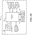
- FIG. 5B provides an illustrative schematic representative of a mobile device 1300 that can be used in conjunction with various embodiments of the present invention.
- Mobile devices 1300 can be operated by various parties.
- a mobile device 1300 may include an antenna 1312, a transmitter 1304 (e.g., radio), a receiver 1306 (e.g., radio), and a processing element 1308 that provides signals to and receives signals from the transmitter 1304 and receiver 1306, respectively.
- a transmitter 1304 e.g., radio
- a receiver 1306 e.g., radio
- a processing element 1308 that provides signals to and receives signals from the transmitter 1304 and receiver 1306, respectively.
- the signals provided to and received from the transmitter 1304 and the receiver 1306, respectively, may include signaling data in accordance with an air interface standard of applicable wireless systems to communicate with various entities, such as the server 1200, the distributed devices 1110, 1120, and/or the like.
- the mobile device 1300 may be capable of operating with one or more air interface standards, communication protocols, modulation types, and access types. More particularly, the mobile device 1300 may operate in accordance with any of a number of wireless communication standards and protocols.
- the mobile device 1300 may operate in accordance with multiple wireless communication standards and protocols, such as GPRS, UMTS, CDMA2000, 1xRTT, WCDMA, TD-SCDMA, LTE, E-UTRAN, EVDO, HSPA, HSDPA, Wi-Fi, WiMAX, UWB, IR protocols, Bluetooth protocols, USB protocols, and/or any other wireless protocol.
- multiple wireless communication standards and protocols such as GPRS, UMTS, CDMA2000, 1xRTT, WCDMA, TD-SCDMA, LTE, E-UTRAN, EVDO, HSPA, HSDPA, Wi-Fi, WiMAX, UWB, IR protocols, Bluetooth protocols, USB protocols, and/or any other wireless protocol.
- the mobile device 1300 may according to various embodiments communicate with various other entities using concepts such as Unstructured Supplementary Service data (USSD), Short Message Service (SMS), Multimedia Messaging Service (MMS), Dual-Tone Multi-Frequency Signaling (DTMF), and/or Subscriber Identity Module Dialer (SIM dialer).
- USSD Unstructured Supplementary Service data
- SMS Short Message Service
- MMS Multimedia Messaging Service
- DTMF Dual-Tone Multi-Frequency Signaling
- SIM dialer Subscriber Identity Module Dialer
- the mobile device 1300 can also download changes, add-ons, and updates, for instance, to its firmware, software (e.g., including executable instructions, applications, program modules), and operating system.
- the mobile device 1300 may include a location determining device and/or functionality.
- the mobile device 1300 may include a GPS module adapted to acquire, for example, latitude, longitude, altitude, geocode, course, and/or speed data.
- the GPS module acquires data, sometimes known as ephemeris data, by identifying the number of satellites in view and the relative positions of those satellites.
- the mobile device 1300 may also comprise a user interface (that can include a display 1316 coupled to a processing element 1308 ) and/or a user input interface (coupled to a processing element 308 ).
- the user input interface can comprise any of a number of devices allowing the mobile device 1300 to receive data, such as a keypad 1318 (hard or soft), a touch display, voice or motion interfaces, or other input device.
- the keypad can include (or cause display of) the conventional numeric (0-9) and related keys (#, *), and other keys used for operating the mobile device 1300 and may include a full set of alphabetic keys or set of keys that may be activated to provide a full set of alphanumeric keys.
- the user input interface can be used, for example, to activate or deactivate certain functions, such as screen savers and/or sleep modes.
- the mobile device 1300 can also include volatile storage or memory 1322 and/or non-volatile storage or memory 1324, which can be embedded and/or may be removable.
- the non-volatile memory may be ROM, PROM, EPROM, EEPROM, flash memory, MMCs, SD memory cards, Memory Sticks, CBRAM, PRAM, FeRAM, RRAM, SONOS, racetrack memory, and/or the like.
- the volatile memory may be RAM, DRAM, SRAM, FPM DRAM, EDO DRAM, SDRAM, DDR SDRAM, DDR2 SDRAM, DDR3 SDRAM, RDRAM, RIMM, DIMM, SIMM, VRAM, cache memory, register memory, and/or the like.
- the volatile and non-volatile storage or memory can store databases, database instances, database mapping systems, data, applications, programs, program modules, scripts, source code, object code, byte code, compiled code, interpreted code, machine code, executable instructions, and/or the like to implement the functions of the mobile device 1300.
- the mobile device 1300 may also include one or more of a camera 1326 and a mobile application 1330.
- the camera 1326 may be configured according to various embodiments as an additional and/or alternative data collection feature, whereby one or more items may be read, stored, and/or transmitted by the mobile device 1300 via the camera.
- the mobile application 1330 may further provide a feature via which various tasks may be performed with the mobile device 1300.
- Various configurations may be provided, as may be desirable for one or more users of the mobile device 1300 and the system 1020 as a whole.
Landscapes
- Chemical & Material Sciences (AREA)
- Engineering & Computer Science (AREA)
- Materials Engineering (AREA)
- Manufacturing & Machinery (AREA)
- Physics & Mathematics (AREA)
- Optics & Photonics (AREA)
- Mechanical Engineering (AREA)
- Analytical Chemistry (AREA)
- Plasma & Fusion (AREA)
- Powder Metallurgy (AREA)
Description
- The present invention relates to an electron beam source and a method for prolonging the lifetime of an electron beam source.
- Freeform fabrication or additive manufacturing is a method for forming three-dimensional articles through successive fusion of chosen parts of powder layers applied to a worktable.
- An additive manufacturing apparatus may comprise a work table on which the three-dimensional article is to be formed, a powder dispenser or powder distributor, arranged to lay down a thin layer of powder on the work table for the formation of a powder bed, a high energy beam for delivering energy to the powder whereby fusion of the powder takes place, elements for control of the energy given off by the energy beam over the powder bed for the formation of a cross section of the three-dimensional article through fusion of parts of the powder bed, and a controlling computer, in which information is stored concerning consecutive cross sections of the three-dimensional article. A three-dimensional article is formed through consecutive fusions of consecutively formed cross sections of powder layers, successively laid down by the powder dispenser. Reference is made to, for example, to
EP 2 911 181 A1 - In additive manufacturing a short manufacturing time and high quality of the finalized product is of outmost importance. What is also important is to reduce servicing of the additive manufacturing apparatus as much as possible. The life time of the cathode element is one thing which constantly requires service in form of exchange when being worn out. It is desirable to extend the lifetime of the cathode element. Today the electron beam source settings is mainly performed manually which may introduce settings which reduces the lifetime from the very outset and/or after a period of time when the performance of the cathode element has changed. Reference is made to, for example,
JP 2005 024343 A - An object of various embodiments of the invention is to provide a method which prolongs the lifetime of an electron beam source. The above-mentioned object is achieved by the features recited in the claims provided herein.
- In a first aspect of various embodiments of the invention it is provided a method for prolonging lifetime of at least one electron beam source, the method comprising the steps of: providing the at least one electron beam source emitting an electron beam, where the electron beam source comprises a cathode, an anode, and a grid between the cathode and anode; setting an electron beam current, a cathode heating power, a grid potential Ug and a cathode potential Uc to predetermined start values, reducing the cathode heating power with a predetermined value and decreasing a Uc - Ug potential difference for maintaining the predetermined electron beam current, detecting an X-ray signal emanating from the electron beam source with at least one X-ray detector, repeating step c and d (the last two steps) until the detected X-ray signal is above a predetermined value, and increasing the cathode heating power by a predetermined safety value from a threshold heating power value which resulted in x-ray signals, emanating from the electron beam source, above the predetermined value.
- An exemplary advantage of various embodiments of the present invention is that it gives much better control of the heating power of the cathode element than prior art technique. Another advantage is that it is possible to adjust the heating power depending on the actual hours the cathode element has been used. Yet another advantage of the present invention is that the heating power may be set optimally individually for different additive manufacturing machines.
- In various example embodiments of the present invention the start value of the electron beam current is between 20-50mA. An exemplary advantage of at least these embodiments is that the method works for any suitable electron beam current which may be sued during additive manufacturing.
- In various example embodiments of the present invention further comprising the step of arranging the X-ray detector in the electron beam source. An exemplary advantage of at least these embodiments is that the detector is arranged for receiving x-rays emanating from the electron beam source only. In case of any background x-ray signal emanating from any other place in the additive manufacturing machine such X-rays may be filtered away easily.
- All examples and exemplary embodiments described herein are non-limiting in nature and thus should not be construed as limiting the scope of the invention described herein. Still further, the advantages described herein, even where identified with respect to a particular exemplary embodiment, should not be necessarily construed in such a limiting fashion.
- The invention will be further described in the following, in a non-limiting way with reference to the accompanying drawings. Same characters of reference are employed to indicate corresponding similar parts throughout the several figures of the drawings:
-
FIG. 1 depicts, in a schematic view, an example embodiment of an electron beam source in which the inventive method may be implemented; -
FIG. 2 depicts, in a schematic view, an example embodiment of an apparatus for producing a three dimensional product which may have an electron beam source according tofigure 1 ; -
FIG. 3 depicts the Cathode potential - grid potential as a function of electron beam current for different emissivity of a filament in an electron beam source; -
FIG. 4 is a block diagram of anexemplary system 1020 according to various embodiments; -
FIG. 5A is a schematic block diagram of aserver 1200 according to various embodiments; and -
FIG. 5B is a schematic block diagram of an exemplarymobile device 1300 according to various embodiments. - Various embodiments of the present invention will now be described more fully hereinafter with reference to the accompanying drawings, in which some, but not all embodiments of the invention are shown. Indeed, embodiments of the invention may be embodied in many different forms and should not be construed as limited to the embodiments set forth herein. Rather, these embodiments are provided so that this disclosure will satisfy applicable legal requirements. Unless otherwise defined, all technical and scientific terms used herein have the same meaning as commonly known and understood by one of ordinary skill in the art to which the invention relates. The term "or" is used herein in both the alternative and conjunctive sense, unless otherwise indicated. Like numbers refer to like elements throughout.
- Still further, to facilitate the understanding of this invention, a number of terms are defined below. Terms defined herein have meanings as commonly understood by a person of ordinary skill in the areas relevant to the present invention. Terms such as "a", "an" and "the" are not intended to refer to only a singular entity, but include the general class of which a specific example may be used for illustration. The terminology herein is used to describe specific embodiments of the invention, but their usage does not delimit the invention, except as outlined in the claims.
- The term "three-dimensional structures" and the like as used herein refer generally to intended or actually fabricated three-dimensional configurations (e.g., of structural material or materials) that are intended to be used for a particular purpose. Such structures, etc. may, for example, be designed with the aid of a three-dimensional CAD system.
-
Figure 2 depicts an embodiment of a freeform fabrication oradditive manufacturing apparatus 21 in which the inventive method according to the present invention may be implemented. - The
apparatus 21 comprising anelectron beam gun 6;deflection coils 7; twopowder hoppers build platform 2; abuild tank 10; apowder distributor 28; apowder bed 5; and avacuum chamber 20. - The
vacuum chamber 20 is capable of maintaining a vacuum environment via a vacuum system, which system may comprise a turbo molecular pump, a scroll pump, an ion pump and one or more valves which are well known to a skilled person in the art and therefore need no further explanation in this context. The vacuum system is controlled by acontrol unit 8. - The
electron beam gun 6 is generating an electron beam which is used for pre heating of the powder, melting or fusing together powder material provided on thebuild platform 2 or post heat treatment of the already fused powder material. At least a portion of theelectron beam gun 6 may be provided in thevacuum chamber 20. Thecontrol unit 8 may be used for controlling and managing the electron beam emitted from theelectron beam gun 6. At least one focusing coil (not shown), at least onedeflection coil 7, an optional coil for astigmatic correction (not shown) and an electron beam power supply (not shown) may be electrically connected to thecontrol unit 8. In an example embodiment of the invention theelectron beam gun 6 may generate a focusable electron beam with an accelerating voltage of about 15-60kV and with a beam power in the range of 3-10kW. The pressure in the vacuum chamber may be 10-3 mbar or lower when building the three-dimensional article by fusing the powder layer by layer with the energy beam. - The
powder hoppers build platform 2 in thebuild tank 10. The powder material may for instance be pure metals or metal alloys such as titanium, titanium alloys, aluminum, aluminum alloys, stainless steel, Co-Cr alloys, nickel based super alloys, etc. - The
powder distributor 28 is arranged to lay down a thin layer of the powder material on thebuild platform 2. During a work cycle thebuild platform 2 will be lowered successively in relation to a fixed point in the vacuum chamber. In order to make this movement possible, thebuild platform 2 is in one embodiment of the invention arranged movably in vertical direction, i.e., in the direction indicated by arrow P. This means that thebuild platform 2 starts in an initial position, in which a first powder material layer of necessary thickness has been laid down. Means for lowering thebuild platform 2 may for instance be through a servo engine equipped with a gear, adjusting screws, etc. The servo engine may be connected to thecontrol unit 8. - An electron beam may be directed over the
build platform 2 causing the first powder layer to fuse in selected locations to form a first cross section of the three-dimensional article 3. The beam is directed over thebuild platform 2 from instructions given by thecontrol unit 8. In thecontrol unit 8 instructions for how to control the electron beam for each layer of the three-dimensional article is stored. The first layer of the threedimensional article 3 may be built on thebuild platform 2, which may be removable, in thepowder bed 5 or on anoptional start plate 16. Thestart plate 16 may be arranged directly on thebuild platform 2 or on top of apowder bed 5 which is provided on thebuild platform 2. - After a first layer is finished, i.e., the fusion of powder material for making a first layer of the three-dimensional article, a second powder layer is provided on the
build platform 2. The thickness of the second layer may be determined by the distance the build platform is lowered in relation to the position where the first layer was built. The second powder layer is in various embodiments distributed according to the same manner as the previous layer. However, there might be alternative methods in the same additive manufacturing machine for distributing powder onto the work table. For instance, a first layer may be provided via afirst powder distributor 28, a second layer may be provided by another powder distributor. The design of the powder distributor is automatically changed according to instructions from thecontrol unit 8. Apowder distributor 28 in the form of a single rake system, i.e., where one rake is catching powder fallen down from both aleft powder hopper 4 and aright powder hopper 14, the rake as such can change design. - After having distributed the second powder layer on the build platform, the energy beam is directed over the work table causing the second powder layer to fuse in selected locations to form a second cross section of the three-dimensional article. Fused portions in the second layer may be bonded to fused portions of the first layer. The fused portions in the first and second layer may be melted together by melting not only the powder in the uppermost layer but also remelting at least a fraction of a thickness of a layer directly below the uppermost layer.
- Sometimes it may be necessary to consider the charge distribution that is created in the powder as the electrons hit the
powder bed 5. The charge distribution density depends on the following parameters: beam current, electron velocity (which is given by the accelerating voltage), beam scanning velocity, powder material and electrical conductivity of the powder, i.e., mainly the electrical conductivity between the powder grains. The latter is in turn a function of several parameters, such as the non-limiting examples of temperature, degree of sintering and powder grain size/size distribution. - Thus, for a given powder, i.e., a powder of a certain material with a certain grain size distribution, and a given accelerating voltage, it is possible, by varying the beam current (and thus the beam power) and the beam scanning velocity, to affect the charge distribution.
- By varying these parameters in a controlled way, the electrical conductivity of the powder can gradually be increased by increasing the temperature of the powder. A powder that has a high temperature obtains a considerably higher conductivity which results in a lower density of the charge distribution since the charges quickly can diffuse over a large region. This effect is enhanced if the powder is allowed to be slightly sintered during a pre-heating process. When the conductivity has become sufficiently high, the powder can be fused together, i.e., melted or fully sintered, with predetermined values of the beam current and beam scanning velocity.
-
Figure 1 depicts, in a schematic view, an exemplary embodiment of an electron beam source in which the inventive method may be implemented. Theelectron beam source 100 comprises acathode 102, agrid 104 and ananode 106. Electrons emitted at thecathode 102 being on negative potential are accelerated towards theanode 106 and finally a target surface 118. Agrid 104 is set at a predetermined distance from thecathode 102. Thecathode 102 may be provided with a heating power which may cause the cathode to heat up, where upon thecathode 102 releases electrons by thermionic emission. The heating power is typically around 5W for a lanthanum hexaboride (LaB6) cathode element. - An
accelerator voltage 160 is provided between the cathode and theanode 106. Theaccelerator voltage 160 causes the emitted electrons from thecathode 102 to accelerate towards theanode 106 thus establishing anelectron beam 120. Theelectron beam 120 may impinge on a substrate surface 118, which may be a powder layer in an additive manufacturing process. In order to guide and focus the electron beam there may further be arranged at least one focusing coil and at least one deflection coil. - In the
electron beam source 100 thegrid 104 is provided between thecathode 102 and theanode 106. Thegrid 104 may be arranged as a plate having an aperture. The aperture may be aligned with thecathode 102. The size of the aperture in thegrid 104 may correspond to a cross section of theelectron beam 120 at the position of thegrid 104. - A
grid voltage 180 may be provided between thegrid 104 and thecathode 102 and may be adjusted between a negative blocking voltage and a full power voltage and thereby adjusting an electron beam current between 0 - maximum electron beam current. InFigure 1 thecathode 102 may be provided with a negative potential Uc of -20kV to -100kY. Afirst connection point 110 of theaccelerator voltage 160 and afirst connection point 114 of thegrid voltage 180 may be fixed to the same potential of -20kV to -100kV. Asecond connection point 108 of theaccelerator voltage 160 may be provided with ground potential. Asecond connection point 112 of thegrid voltage 180 may be varied between the negative blocking voltage and the full power voltage. Asecond control unit 150 may be controlling the negative potential Ug on thesecond connection point 112 of the grid voltage in order to adjust the electron beam current to a desired value. Thesecond control unit 150 may be a physically separate control unit in connection with thecontrol unit 8 or fully integrated in thecontrol unit 8. - The target surface 118 may be set to ground potential or a positive potential. The
electron beam source 100 may also comprise means 170 for detecting the actual electron beam current. An example means for detecting the electron beam current on the target surface may be to detect the actual loading of the high voltage source providing theaccelerator voltage 160, indicated bybox 170 inFigure 1 . This may be done by simply measuring the electron beam passing between the first and second connection points 110 and 108 respectively. If the cathode is provided with a fixed negative voltage of -60kV the negative blocking voltage may be around -61kV, i.e., thesecond connection point 112 of the grid voltage is set at -61kV and thefirst connection point 114 is set to -60kV, for blocking the electrons by thegrid 104. If starting to decrease the negative blocking voltage at thesecond connection point 112, some of the electrons emitted from the cathode will be allowed to pass thegrid 104. By varying the grid voltage in this example embodiment between -61kV to ∼-60kV, when the cathode is provided with a fixed negative potential of -60kV, the electron beam current may vary from 0mA - maximum electron beam current which may be 25mA for a predetermined size and shape of the cathode and a predetermined size and shape of the aperture in thegrid 104. Other accelerator voltages and/or other size, shape and emissivity of the cathode and/or other size and shape of the aperture in the grid may affect the maximum electron beam current to be higher or lower than the exemplified 25mA. -
Figure 3 depicts the grid potential - cathode potential as a function of electron beam current for different emissivity of a filament. When thegrid voltage 180 is at a sufficiently high negative potential, i.e., the potential onconnection point 112 is provided with a sufficient negative potential (negative blocking potential) compared to the negative potential onconnection point 114, the electrons emanating from thecathode 102 will be blocked (repelled) by the negative potential on thegrid 104 resulting in no electrons passing through the aperture in thegrid 104. In such a case we are at the leftmost position in the graph inFigure 3 , i.e., zero electron beam current. As the potential difference between thecathode 102 andgrid 104 is decreasing the electron beam current is increasing, i.e., we are moving to the right in the graph inFigure 3 . Uc represents the cathode potential and UG represents the grid potential. - A
cathode 102 at different temperatures may emanate different amounts of electrons. InFigure 3 it is illustrated 4different graphs first graph 310 may represent a cathode at a first temperature. Asecond graph 320 may represent a cathode at a second temperature. Athird graph 330 may represent a cathode at a third temperature. Afourth graph 310 may represent a cathode at a fourth temperature. The first temperature < the second temperature < the third temperature < the fourth temperature. Notably the temperature of the cathode may not be the only parameter that affects the numbers of emanating electrons. When the cathode is used its emissivity of electron may change in a similar manner as depicted inFigure 3 . An unused cathode may be represented bygraph 340. The more thecathode 102 is used the last portion of the graph is shifted to the left. A combination of a change in temperature of the cathode and the degree of use may also be represented by the different graphs inFigure 3 , i.e., for relatively cold cathodes and well used the last portion will be shifted to the left and for a relatively hot and new cathode the graph will be shifted to the right. - The graph in
Figure 3 may be defined by applying a predetermined number of different Uc - Ug potentials and measuring the resulting electron beam current for the Uc - Ug potentials. The graph may be approximated by a mathematical expression, for instance a polynomial which is fitted to the graph. - The invention is how to prolong the life time of the cathode element. If providing an excessive amount of heating power the lifetime of the cathode element is heavily reduced. The invention is about how to determine the lowest acceptable heating power of the cathode element without affecting the electron beam current range of the electron beam source. If looking at
figure 3 , one needs to determine when the Uc-Ug starts to change abruptly for a specific electron beam current denoted by 310', 320', 330'. Since x-rays are created instantly as the electron beam hits the internal structure of the electron beam source it is a very good measure of an electron beam path within the electron beam source which is not correct. A very small amount of the electron beam is needed for creating a detectable X-ray signal. - For purposes of clarity, it is noted that the internal structure of the electron beam source, as reference above and herein-throughout may be a grid plate, an electron tube arranged as a last/final component in the electron beam source, or any component in the electron beam source.
- The idea is to use an
X-ray detector 190 provided in the electron beam source for detecting X-rays emanating from the electron beam source. Obviously x-rays are created when the electron beam is hitting the substrate 118 but the X-ray detector is out of sight from the x-rays and/or the x-rays emanating from the substrate will only create a background X-ray noise which is known and can be eliminated from the detected x-ray signal indetector 190. - In a first step the electron beam source is set to a predetermined electron beam current using a predetermined cathode hating power together with a predetermined grid potential Ug and a predetermined cathode potential Uc. The cathode potential may be kept constant throughout the determination of the heating power of the cathode element. An X-ray signal is detected by the
X-ray detector 190. If the X-ray signal is below a predetermined value the cathode heating power may be reduced by a predetermined heating power step. In order to keep the electron beam current constant when the heating power is reduced the Uc-Ug potential needs to be decreased. The heating power step may for instance be 0.05W. The X-ray detector is again detecting the X-ray signal. If the X-ray signal is still below the predetermined value a further decrease in heating power is performed together with a new decrease in Uc-Ug potential and yet a new X-ray measurement is made. However, if the X-ray signal is above a predetermined value, it means that the heating power is too low for creating a predetermined electron beam current. As the heating power is reduced the Uc-Ug potential is also reduced in order to maintain the constant electron beam current. At a certain point the Uc-Ug potential will be so low that electron emissions from the cathode element will hit internal elements within the electron beam source and thereby create X-ray emission. A relatively low grid potential from a relatively "cold" cathode element will result in electron emission in direction not only towards the substrate but also electron emission which will hit internal elements within the electron beam source. - X-rays detected by the
detector 190 are mainly emanating from the electron beam source as such. This means that when the electron beam hits the internal structure of the electron beam source before the electron beam is leaving the electron beam source. One or a plurality of detectors may be used. A detector may be arranged for receiving x-rays signals from a particular area of the electron beam source. If the complete electron beam source is to be detected more than one x-ray detector may be needed. - The risk of hitting the internal structure with the complete electron beam is reduced and/or eliminated if the starting value of the heating power is chosen in a safe interval where one knows by experience that no x-rays should be detected. In the exemplified embodiment a Uc-Ug of about 300 V or higher and a heating power above 5w may be a good starting point for a lanthanum hexaboride cathode element. If the heating power is reduced by predetermined steps closely enough spaced apart the method will prohibit full impact of the electron beam into the internal structure of the electron beam source. This may reduce the contamination of cathode element and thereby further increase its lifetime.
- The constant electron beam current used may be the maximum current to be used in the additive manufacturing process. If the heating power is determined not to create x-ray emissions above a predetermined level for the maximum electron beam current, then electron beam currents lower than the maximum electron beam current will also not create X-ray emission above the level.
- A predetermined safety value is added to a threshold heating power, which threshold heating power resulted in the X-ray signal above the predetermined value.
- The X-ray measurement may be done prior to starting to additively manufacture a three dimensional article. The x-ray measurement may also be made during preheating powder material during a build or post heat treatment of already fused material during a build. In another example embodiment the X-ray measurement is made during powder distribution. The x-ray emanating from the electron beam source may also be detected during the fusion process.
- A usable range of heating powers of a cathode element of the electron beam source may be defined as follows. A lowest value in the range may be the heating power of the cathode element for a given electron beam current which creates an X-ray signal from the electron beam source which is lower than a predetermined value. The predetermined value may be 0.0001mSv. The upper limit may be chosen arbitrary. However, the higher the heating power above the lowest value the shorter the life time of the cathode element.
- A sign of a worn out cathode element may be a too large deviation from the previous cathode heating power setting. This may be used as a warning for the operator of the additive manufacturing machine that the cathode element needs to be replaced if the heating power is increased above a predetermined percentage of the previous heating power setting. In an example embodiment a maximum value in which the heating power may be increased from the previous setting without having to be replaced may be 0.3W.
- In an arrangement where the electron beam is bent in order to impinge perpendicular onto the substrate, i.e., in a case where the electron beams emanating from the electron beam source is travelling in a direction at an angle different to 90 degrees from a substrate surface 118. X-rays emanating from the electron beam source including electron beam bending coils, may be a measure of good or bad electron beam path. An X-ray signal may be a sign of an electron beam hitting the internal structure of the electron beam source before it is leaving the electron beam source.
- The start value of the electron beam current may be 20-50mA.
- An updating of the heating power may be performed regularly during the manufacturing of the three-dimensional article. In an example embodiment the updating of the heating power may be performed in regular time intervals of for
instance 5 minutes. In an alternative embodiment the updating is performed only during specific process steps such as powder distribution, preheating of powder material in order to reach a predetermined temperature interval or post heat treatment of already fused powder material in order to maintain the temperature of the three-dimensional article within a predetermined temperature interval. - The heating power is in an example embodiment reduced in steps of 0.05W. A larger step may introduce a risk of hitting the internal structure with a too large amount of the electron beam which may cause unwanted contamination and reduced lifetime of the cathode element. A too small step may require too much time before knowing which heating power to use.
- In an example embodiment a triod electron beam source may be used for forming a three-dimensional article through successively depositing individual layers of powder material that are fused together so as to form the article. The triod electron beam source comprises an anode, a cathode and a grid. A cathode heating power is kept at a predetermined value above a threshold heating value which threshold heating value creates a predetermined X-ray signal emanating from the triod electron beam source. The three dimensional article may be fused using the cathode heating power kept at the predetermined value above the threshold heating value.
- In another aspect of the invention it is provided a program element configured and arranged when executed on a computer to implement a method for forming a three-dimensional article through successively depositing individual layers of powder material that are fused together so as to form the article, the method comprising the steps of: providing at least one electron beam source emitting an electron beam for heating and/or fusing the powder material, where the electron beam source comprising a cathode, an anode, and a grid between the cathode and anode, controlling the electron beam source in a first mode when the formation of the three dimensional article is in a first process step, controlling the electron beam source in a second mode when the formation of the three dimensional article is in a second process step, wherein an electron beam current from the electron beam source is controlled in a feed-forward mode in the first mode and the electron beam current is controlled in a feed-back mode in the second mode. The program may be installed in a computer readable storage medium. The computer readable storage medium may be the
control unit 8, thecontrol unit 150, or another separate and distinct control unit. The computer readable storage medium and the program element, which may comprise computer-readable program code portions embodied therein, may further be contained within a non-transitory computer program product. Further details regarding these features and configurations are provided, in turn, below. - As mentioned, various embodiments of the present invention may be implemented in various ways, including as non-transitory computer program products. A computer program product may include a non-transitory computer-readable storage medium storing applications, programs, program modules, scripts, source code, program code, object code, byte code, compiled code, interpreted code, machine code, executable instructions, and/or the like (also referred to herein as executable instructions, instructions for execution, program code, and/or similar terms used herein interchangeably). Such non-transitory computer-readable storage media include all computer-readable media (including volatile and non-volatile media).
- In one embodiment, a non-volatile computer-readable storage medium may include a floppy disk, flexible disk, hard disk, solid-state storage (SSS) (e.g., a solid state drive (SSD), solid state card (SSC), solid state module (SSM)), enterprise flash drive, magnetic tape, or any other non-transitory magnetic medium, and/or the like. A non-volatile computer-readable storage medium may also include a punch card, paper tape, optical mark sheet (or any other physical medium with patterns of holes or other optically recognizable indicia), compact disc read only memory (CD-ROM), compact disc compact disc-rewritable (CD-RW), digital versatile disc (DVD), Blu-ray disc (BD), any other non-transitory optical medium, and/or the like. Such a non-volatile computer-readable storage medium may also include read-only memory (ROM), programmable read-only memory (PROM), erasable programmable read-only memory (EPROM), electrically erasable programmable read-only memory (EEPROM), flash memory (e.g., Serial, NAND, NOR, and/or the like), multimedia memory cards (MMC), secure digital (SD) memory cards, SmartMedia cards, CompactFlash (CF) cards, Memory Sticks, and/or the like. Further, a non-volatile computer-readable storage medium may also include conductive-bridging random access memory (CBRAM), phase-change random access memory (PRAM), ferroelectric random-access memory (FeRAM), non-volatile random-access memory (NVRAM), magnetoresistive random-access memory (MRAM), resistive random-access memory (RRAM), Silicon-Oxide-Nitride-Oxide-Silicon memory (SONOS), floating junction gate random access memory (FJG RAM), Millipede memory, racetrack memory, and/or the like.
- In one embodiment, a volatile computer-readable storage medium may include random access memory (RAM), dynamic random access memory (DRAM), static random access memory (SRAM), fast page mode dynamic random access memory (FPM DRAM), extended data-out dynamic random access memory (EDO DRAM), synchronous dynamic random access memory (SDRAM), double data rate synchronous dynamic random access memory (DDR SDRAM), double data rate type two synchronous dynamic random access memory (DDR2 SDRAM), double data rate type three synchronous dynamic random access memory (DDR3 SDRAM), Rambus dynamic random access memory (RDRAM), Twin Transistor RAM (TTRAM), Thyristor RAM (T-RAM), Zero-capacitor (Z-RAM), Rambus in-line memory module (RIMM), dual in-line memory module (DIMM), single in-line memory module (SIMM), video random access memory VRAM, cache memory (including various levels), flash memory, register memory, and/or the like. It will be appreciated that where embodiments are described to use a computer-readable storage medium, other types of computer-readable storage media may be substituted for or used in addition to the computer-readable storage media described above.
- As should be appreciated, various embodiments of the present invention may also be implemented as methods, apparatus, systems, computing devices, computing entities, and/or the like, as have been described elsewhere herein. As such, embodiments of the present invention may take the form of an apparatus, system, computing device, computing entity, and/or the like executing instructions stored on a computer-readable storage medium to perform certain steps or operations. However, embodiments of the present invention may also take the form of an entirely hardware embodiment performing certain steps or operations.
- Various embodiments are described below with reference to block diagrams and flowchart illustrations of apparatuses, methods, systems, and computer program products. Thus, it should be understood that each block of the block diagrams and flowchart illustrations may be implemented in the form of a computer program product, an entirely hardware embodiment, a combination of hardware and computer program products, and/or apparatus, systems, computing devices, computing entities, and/or the like carrying out instructions, operations, steps, and similar words used interchangeably (e.g., the executable instructions, instructions for execution, program code, and/or the like) on a computer-readable storage medium for execution. For example, retrieval, loading, and execution of code may be performed sequentially such that one instruction is retrieved, loaded, and executed at a time. In some exemplary embodiments, retrieval, loading, and/or execution may be performed in parallel such that multiple instructions are retrieved, loaded, and/or executed together. Thus, such embodiments can produce specifically-configured machines performing the steps or operations specified in the block diagrams and flowchart illustrations. Accordingly, the block diagrams and flowchart illustrations support various combinations of embodiments for performing the specified instructions, operations, or steps.
- These computer program instructions may also be stored in a computer-readable memory that can direct a computer or other programmable data processing apparatus to function in a particular manner, such that the instructions stored in the computer-readable memory produce an article of manufacture including computer-readable instructions for implementing the functionality specified in the flowchart block or blocks. The computer program instructions may also be loaded onto a computer or other programmable data processing apparatus to cause a series of operational steps to be performed on the computer or other programmable apparatus to produce a computer-implemented process such that the instructions that execute on the computer or other programmable apparatus provide operations for implementing the functions specified in the flowchart block or blocks.
- Accordingly, blocks of the block diagrams and flowchart illustrations support various combinations for performing the specified functions, combinations of operations for performing the specified functions and program instructions for performing the specified functions. It should also be understood that each block of the block diagrams and flowchart illustrations, and combinations of blocks in the block diagrams and flowchart illustrations, could be implemented by special purpose hardware-based computer systems that perform the specified functions or operations, or combinations of special purpose hardware and computer instructions.
-
Figure 4 is a block diagram of anexemplary system 1020 that can be used in conjunction with various embodiments of the present invention. In at least the illustrated embodiment, thesystem 1020 may include one or morecentral computing devices 1110, one or more distributedcomputing devices 1120, and one or more distributed handheld ormobile devices 1300, all configured in communication with a central server 1200 (or control unit) via one ormore networks 1130. WhileFigure 4 illustrates the various system entities as separate, standalone entities, the various embodiments are not limited to this particular architecture. - According to various embodiments of the present invention, the one or
more networks 1130 may be capable of supporting communication in accordance with any one or more of a number of second-generation (2G), 2.5G, third-generation (3G), and/or fourth-generation (4G) mobile communication protocols, or the like. More particularly, the one ormore networks 1130 may be capable of supporting communication in accordance with 2G wireless communication protocols IS-136 (TDMA), GSM, and IS-95 (CDMA). Also, for example, the one ormore networks 1130 may be capable of supporting communication in accordance with 2.5G wireless communication protocols GPRS, Enhanced Data GSM Environment (EDGE), or the like. In addition, for example, the one ormore networks 1130 may be capable of supporting communication in accordance with 3G wireless communication protocols such as Universal Mobile Telephone System (UMTS) network employing Wideband Code Division Multiple Access (WCDMA) radio access technology. Some narrow-band AMPS (NAMPS), as well as TACS, network(s) may also benefit from embodiments of the present invention, as should dual or higher mode mobile stations (e.g., digital/analog or TDMA/CDMA/analog phones). As yet another example, each of the components of thesystem 5 may be configured to communicate with one another in accordance with techniques such as, for example, radio frequency (RF), Bluetooth™, infrared (IrDA), or any of a number of different wired or wireless networking techniques, including a wired or wireless Personal Area Network ("PAN"), Local Area Network ("LAN"), Metropolitan Area Network ("MAN"), Wide Area Network ("WAN"), or the like. - Although the device(s) 1110-1300 are illustrated in
Figure 4 as communicating with one another over thesame network 1130, these devices may likewise communicate over multiple, separate networks. - According to one embodiment, in addition to receiving data from the
server 1200, the distributeddevices devices devices more networks 1130. - In various embodiments, the
server 1200 includes various systems for performing one or more functions in accordance with various embodiments of the present invention, including those more particularly shown and described herein. It should be understood, however, that theserver 1200 might include a variety of alternative devices for performing one or more like functions, without departing from the spirit and scope of the present invention. For example, at least a portion of theserver 1200, in certain embodiments, may be located on the distributed device(s) 1110, 1120, and/or the handheld or mobile device(s) 1300, as may be desirable for particular applications. As will be described in further detail below, in at least one embodiment, the handheld or mobile device(s) 1300 may contain one or moremobile applications 1330 which may be configured so as to provide a user interface for communication with theserver 1200, all as will be likewise described in further detail below. -
Figure 5A is a schematic diagram of theserver 1200 according to various embodiments. Theserver 1200 includes aprocessor 1230 that communicates with other elements within the server via a system interface orbus 1235. Also included in theserver 1200 is a display/input device 1250 for receiving and displaying data. This display/input device 1250 may be, for example, a keyboard or pointing device that is used in combination with a monitor. Theserver 1200 further includes memory 1220, which preferably includes both read only memory (ROM) 1226 and random access memory (RAM) 1222. The server'sROM 1226 is used to store a basic input/output system 1224 (BIOS), containing the basic routines that help to transfer information between elements within theserver 1200. Various ROM and RAM configurations have been previously described herein. - In addition, the
server 1200 includes at least one storage device or program storage 210, such as a hard disk drive, a floppy disk drive, a CD Rom drive, or optical disk drive, for storing information on various computer-readable media, such as a hard disk, a removable magnetic disk, or a CD-ROM disk. As will be appreciated by one of ordinary skill in the art, each of thesestorage devices 1210 are connected to thesystem bus 1235 by an appropriate interface. Thestorage devices 1210 and their associated computer-readable media provide nonvolatile storage for a personal computer. As will be appreciated by one of ordinary skill in the art, the computer-readable media described above could be replaced by any other type of computer-readable media known in the art. Such media include, for example, magnetic cassettes, flash memory cards, digital video disks, and Bernoulli cartridges. - Although not shown, according to an embodiment, the
storage device 1210 and/or memory of theserver 1200 may further provide the functions of a data storage device, which may store historical and/or current delivery data and delivery conditions that may be accessed by theserver 1200. In this regard, thestorage device 1210 may comprise one or more databases. The term "database" refers to a structured collection of records or data that is stored in a computer system, such as via a relational database, hierarchical database, or network database and as such, should not be construed in a limiting fashion. - A number of program modules (e.g., exemplary modules 1400-1700) comprising, for example, one or more computer-readable program code portions executable by the
processor 1230, may be stored by thevarious storage devices 1210 and within RAM 1222. Such program modules may also include anoperating system 1280. In these and other embodiments, thevarious modules server 1200 with the assistance of theprocessor 1230 andoperating system 1280. In still other embodiments, it should be understood that one or more additional and/or alternative modules may also be provided, without departing from the scope and nature of the present invention. - In various embodiments, the
program modules server 1200 and are configured to generate one or more graphical user interfaces, reports, instructions, and/or notifications/alerts, all accessible and/or transmittable to various users of thesystem 1020. In certain embodiments, the user interfaces, reports, instructions, and/or notifications/alerts may be accessible via one ormore networks 1130, which may include the Internet or other feasible communications network, as previously discussed. - In various embodiments, it should also be understood that one or more of the
modules devices modules - Also located within the
server 1200 is anetwork interface 1260 for interfacing and communicating with other elements of the one ormore networks 1130. It will be appreciated by one of ordinary skill in the art that one or more of theserver 1200 components may be located geographically remotely from other server components. Furthermore, one or more of theserver 1200 components may be combined, and/or additional components performing functions described herein may also be included in the server. - While the foregoing describes a
single processor 1230, as one of ordinary skill in the art will recognize, theserver 1200 may comprise multiple processors operating in conjunction with one another to perform the functionality described herein. In addition to the memory 1220, theprocessor 1230 can also be connected to at least one interface or other means for displaying, transmitting and/or receiving data, content or the like. In this regard, the interface(s) can include at least one communication interface or other means for transmitting and/or receiving data, content or the like, as well as at least one user interface that can include a display and/or a user input interface, as will be described in further detail below. The user input interface, in turn, can comprise any of a number of devices allowing the entity to receive data from a user, such as a keypad, a touch display, a joystick or other input device. - As will be understood, the processing element 305 may be embodied in a number of different ways. For example, the processing element or processor may be embodied as one or more complex programmable logic devices (CPLDs), microprocessors, multi-core processors, coprocessing entities, application-specific instruction-set processors (ASIPs), and/or controllers. Further, the processing element may be embodied as one or more other processing devices or circuitry. The term circuitry may refer to an entirely hardware embodiment or a combination of hardware and computer program products. Thus, the processing element may be embodied as integrated circuits, application specific integrated circuits (ASICs), field programmable gate arrays (FPGAs), programmable logic arrays (PLAs), hardware accelerators, other circuitry, and/or the like. As will therefore be understood, the processing element may be configured for a particular use or configured to execute instructions stored in volatile or non-volatile media or otherwise accessible to the processing element. As such, whether configured by hardware or computer program products, or by a combination thereof, the processing element may be capable of performing steps or operations according to embodiments of the present invention when configured accordingly.
- Still further, while reference is made to the "server" 1200, as one of ordinary skill in the art will recognize, embodiments of the present invention are not limited to traditionally defined server architectures. Still further, the system of embodiments of the present invention is not limited to a single server, or similar network entity or mainframe computer system. Other similar architectures including one or more network entities operating in conjunction with one another to provide the functionality described herein may likewise be used without departing from the spirit and scope of embodiments of the present invention. For example, a mesh network of two or more personal computers (PCs), similar electronic devices, or handheld portable devices, collaborating with one another to provide the functionality described herein in association with the
server 1200 may likewise be used without departing from the spirit and scope of embodiments of the present invention. - According to various embodiments, many individual steps of a process may or may not be carried out utilizing the computer systems and/or servers described herein, and the degree of computer implementation may vary, as may be desirable and/or beneficial for one or more particular applications.
-
Figure 5B provides an illustrative schematic representative of amobile device 1300 that can be used in conjunction with various embodiments of the present invention.Mobile devices 1300 can be operated by various parties. As shown inFigure 5B , amobile device 1300 may include anantenna 1312, a transmitter 1304 (e.g., radio), a receiver 1306 (e.g., radio), and aprocessing element 1308 that provides signals to and receives signals from thetransmitter 1304 andreceiver 1306, respectively. - The signals provided to and received from the
transmitter 1304 and thereceiver 1306, respectively, may include signaling data in accordance with an air interface standard of applicable wireless systems to communicate with various entities, such as theserver 1200, the distributeddevices mobile device 1300 may be capable of operating with one or more air interface standards, communication protocols, modulation types, and access types. More particularly, themobile device 1300 may operate in accordance with any of a number of wireless communication standards and protocols. In a particular embodiment, themobile device 1300 may operate in accordance with multiple wireless communication standards and protocols, such as GPRS, UMTS, CDMA2000, 1xRTT, WCDMA, TD-SCDMA, LTE, E-UTRAN, EVDO, HSPA, HSDPA, Wi-Fi, WiMAX, UWB, IR protocols, Bluetooth protocols, USB protocols, and/or any other wireless protocol. - Via these communication standards and protocols, the
mobile device 1300 may according to various embodiments communicate with various other entities using concepts such as Unstructured Supplementary Service data (USSD), Short Message Service (SMS), Multimedia Messaging Service (MMS), Dual-Tone Multi-Frequency Signaling (DTMF), and/or Subscriber Identity Module Dialer (SIM dialer). Themobile device 1300 can also download changes, add-ons, and updates, for instance, to its firmware, software (e.g., including executable instructions, applications, program modules), and operating system. - According to one embodiment, the
mobile device 1300 may include a location determining device and/or functionality. For example, themobile device 1300 may include a GPS module adapted to acquire, for example, latitude, longitude, altitude, geocode, course, and/or speed data. In one embodiment, the GPS module acquires data, sometimes known as ephemeris data, by identifying the number of satellites in view and the relative positions of those satellites. - The
mobile device 1300 may also comprise a user interface (that can include adisplay 1316 coupled to a processing element 1308) and/or a user input interface (coupled to a processing element 308). The user input interface can comprise any of a number of devices allowing themobile device 1300 to receive data, such as a keypad 1318 (hard or soft), a touch display, voice or motion interfaces, or other input device. In embodiments including akeypad 1318, the keypad can include (or cause display of) the conventional numeric (0-9) and related keys (#, *), and other keys used for operating themobile device 1300 and may include a full set of alphabetic keys or set of keys that may be activated to provide a full set of alphanumeric keys. In addition to providing input, the user input interface can be used, for example, to activate or deactivate certain functions, such as screen savers and/or sleep modes. - The
mobile device 1300 can also include volatile storage ormemory 1322 and/or non-volatile storage ormemory 1324, which can be embedded and/or may be removable. For example, the non-volatile memory may be ROM, PROM, EPROM, EEPROM, flash memory, MMCs, SD memory cards, Memory Sticks, CBRAM, PRAM, FeRAM, RRAM, SONOS, racetrack memory, and/or the like. The volatile memory may be RAM, DRAM, SRAM, FPM DRAM, EDO DRAM, SDRAM, DDR SDRAM, DDR2 SDRAM, DDR3 SDRAM, RDRAM, RIMM, DIMM, SIMM, VRAM, cache memory, register memory, and/or the like. The volatile and non-volatile storage or memory can store databases, database instances, database mapping systems, data, applications, programs, program modules, scripts, source code, object code, byte code, compiled code, interpreted code, machine code, executable instructions, and/or the like to implement the functions of themobile device 1300. - The
mobile device 1300 may also include one or more of acamera 1326 and amobile application 1330. Thecamera 1326 may be configured according to various embodiments as an additional and/or alternative data collection feature, whereby one or more items may be read, stored, and/or transmitted by themobile device 1300 via the camera. Themobile application 1330 may further provide a feature via which various tasks may be performed with themobile device 1300. Various configurations may be provided, as may be desirable for one or more users of themobile device 1300 and thesystem 1020 as a whole. - It will be appreciated that many variations of the above systems and methods are possible, and that deviation from the above embodiments are possible, but yet within the scope of the claims. Many modifications and other embodiments of the invention set forth herein will come to mind to one skilled in the art to which these inventions pertain having the benefit of the teachings presented in the foregoing descriptions and the associated drawings. Such modifications may, for example, other materials than metallic powder, such as the non-limiting examples of: electrically conductive polymers and powder of electrically conductive ceramics. Therefore, it is to be understood that the inventions are not to be limited to the specific
embodiments disclosed and that modifications and other embodiments are intended to be included within the scope of the appended claims. Although specific terms are employed herein, they are used in a generic and descriptive sense only and not for purposes of limitation.
Claims (13)
- A method for prolonging lifetime of at least one electron beam source, the method comprising the steps of:providing the at least one electron beam source emitting an electron beam, wherein the electron beam source comprises a cathode, an anode, and a grid between the cathode and anode;setting an electron beam current, a cathode heating power, a grid potential Ug and a cathode potential Uc to predetermined start values;reducing the cathode heating power with a predetermined value and decreasing a Uc-Ug potential difference for maintaining the predetermined electron beam current;detecting an X-ray signal emanating from the electron beam source with at least one X-ray detector;repeating said reducing and detecting steps until the detected X-ray signal is above a predetermined value; andincreasing the cathode heating power by a predetermined safety value from a threshold heating power value which resulted in x-ray signals, emanating from the electron beam source, above the predetermined value.
- The method according to claim 1, wherein the start value of the electron beam current is between 20-50mA.
- The method according to claim 1, further comprising the step of arranging the X-ray detector in the electron beam source.
- The method according to claim 1, wherein the start value of the cathode heating power is about 5W.
- The method according to claim 1, wherein the predetermined value in which the cathode heating power is reduced is in steps of 0.05W.
- The method according to claim 1, wherein the predetermined safety value is between 0.4 - 0.8W.
- The method according to claim 1, further comprising the step of filtering out any x-ray signal not emanating from the electron beam source.
- An electron beam source emitting an electron beam, where the electron beam source comprises a cathode (102), an anode (106), and a grid (104) between the cathode and anode; an X-ray detector (190) for detecting x-rays emanating from the at least one electron beam source; and
at least one control unit (150), the at least one control unit being configured for:setting an electron beam current, a cathode heating power, a grid potential Ug and a cathode potential Uc to predetermined start values,reducing the cathode heating power with a predetermined value and decreasing a Uc-Ug potential difference for maintaining the predetermined electron beam current,detecting, via the at least one X-ray detector, X-ray signals emanating from the electron beam source,repeating the reducing and detecting steps until the detected X-ray signal is above a predetermined value, andincreasing the cathode heating power by a predetermined safety value from a threshold heating power value which resulted in x-ray signals, emanating from the electron beam source, above the predetermined value, so as to establish a usable range of heating powers of a cathode element of the electron beam source. - The electron beam source according to claim 8, wherein the start value of the electron beam current is between 20-50mA.
- The electron beam source according to claim 8, wherein the X-ray detector is positioned in the electron beam source.
- The electron beam source according to claim 8, wherein at least one of:the start value of the cathode heating power is about 5W;the predetermined safety value is between 0.4 - 0.8W; orthe predetermined value in which the cathode heating power is reduced is in steps of 0.05W.
- A computer program product comprising at least one non-transitory computer-readable storage medium having computer-readable program code portions embodied therein, the computer-readable program code portions comprising at least one executable portion configured for:setting an electron beam current, a cathode heating power, a grid potential Ug and a cathode potential Uc to predetermined start values;reducing the cathode heating power with a predetermined value and decreasing a Uc-Ug potential difference for maintaining the predetermined electron beam currentdetecting X-ray signal from the electron beam source with an X-ray detector;repeating the reducing and detecting step until the detected X-ray signal is above a predetermined value; andincreasing the cathode heating power by a predetermined value from the value which resulted in x-ray signals above the predetermined value and using the electron beam for forming a three-dimensional article through successively depositing individual layers of powder material that are fused together so as to form the article.
- The computer program product of Claim 12, wherein the at least one executable portion is further configured for filtering out any x-ray signal not emanating from the electron beam source.
Applications Claiming Priority (3)
| Application Number | Priority Date | Filing Date | Title |
|---|---|---|---|
| US201562256525P | 2015-11-17 | 2015-11-17 | |
| US15/290,635 US10525531B2 (en) | 2015-11-17 | 2016-10-11 | Additive manufacturing of three-dimensional articles |
| PCT/EP2016/074575 WO2017084811A1 (en) | 2015-11-17 | 2016-10-13 | Additive manufacturing of three-dimensional articles |
Publications (2)
| Publication Number | Publication Date |
|---|---|
| EP3378089A1 EP3378089A1 (en) | 2018-09-26 |
| EP3378089B1 true EP3378089B1 (en) | 2019-09-18 |
Family
ID=58690478
Family Applications (1)
| Application Number | Title | Priority Date | Filing Date |
|---|---|---|---|
| EP16781437.5A Active EP3378089B1 (en) | 2015-11-17 | 2016-10-13 | Electron beam source and method for operating the same |
Country Status (5)
| Country | Link |
|---|---|
| US (1) | US10525531B2 (en) |
| EP (1) | EP3378089B1 (en) |
| JP (1) | JP6793191B2 (en) |
| CN (1) | CN108541332B (en) |
| WO (1) | WO2017084811A1 (en) |
Families Citing this family (47)
| Publication number | Priority date | Publication date | Assignee | Title |
|---|---|---|---|---|
| EP2231352B1 (en) | 2008-01-03 | 2013-10-16 | Arcam Ab | Method and apparatus for producing three-dimensional objects |
| KR101596432B1 (en) | 2009-07-15 | 2016-02-22 | 아르켐 에이비 | Method and apparatus for producing three-dimensional objects |
| EP2477768B1 (en) | 2009-09-17 | 2019-04-17 | Sciaky Inc. | Electron beam layer manufacturing |
| EP2555902B1 (en) | 2010-03-31 | 2018-04-25 | Sciaky Inc. | Raster methodology for electron beam layer manufacturing using closed loop control |
| EP2797730B2 (en) | 2011-12-28 | 2020-03-04 | Arcam Ab | Method and apparatus for detecting defects in freeform fabrication |
| US10189086B2 (en) | 2011-12-28 | 2019-01-29 | Arcam Ab | Method and apparatus for manufacturing porous three-dimensional articles |
| CN104853901B (en) | 2012-12-17 | 2018-06-05 | 阿卡姆股份公司 | Added material manufacturing method and equipment |
| US9550207B2 (en) | 2013-04-18 | 2017-01-24 | Arcam Ab | Method and apparatus for additive manufacturing |
| US9676032B2 (en) | 2013-09-20 | 2017-06-13 | Arcam Ab | Method for additive manufacturing |
| US10434572B2 (en) | 2013-12-19 | 2019-10-08 | Arcam Ab | Method for additive manufacturing |
| US9802253B2 (en) | 2013-12-16 | 2017-10-31 | Arcam Ab | Additive manufacturing of three-dimensional articles |
| US10130993B2 (en) | 2013-12-18 | 2018-11-20 | Arcam Ab | Additive manufacturing of three-dimensional articles |
| US9789563B2 (en) | 2013-12-20 | 2017-10-17 | Arcam Ab | Method for additive manufacturing |
| US9789541B2 (en) | 2014-03-07 | 2017-10-17 | Arcam Ab | Method for additive manufacturing of three-dimensional articles |
| US20150283613A1 (en) | 2014-04-02 | 2015-10-08 | Arcam Ab | Method for fusing a workpiece |
| US9341467B2 (en) | 2014-08-20 | 2016-05-17 | Arcam Ab | Energy beam position verification |
| US20160167303A1 (en) | 2014-12-15 | 2016-06-16 | Arcam Ab | Slicing method |
| US9721755B2 (en) | 2015-01-21 | 2017-08-01 | Arcam Ab | Method and device for characterizing an electron beam |
| US11014161B2 (en) | 2015-04-21 | 2021-05-25 | Arcam Ab | Method for additive manufacturing |
| US10807187B2 (en) | 2015-09-24 | 2020-10-20 | Arcam Ab | X-ray calibration standard object |
| US11571748B2 (en) | 2015-10-15 | 2023-02-07 | Arcam Ab | Method and apparatus for producing a three-dimensional article |
| US10610930B2 (en) | 2015-11-18 | 2020-04-07 | Arcam Ab | Additive manufacturing of three-dimensional articles |
| US11247274B2 (en) | 2016-03-11 | 2022-02-15 | Arcam Ab | Method and apparatus for forming a three-dimensional article |
| US11325191B2 (en) | 2016-05-24 | 2022-05-10 | Arcam Ab | Method for additive manufacturing |
| US10549348B2 (en) | 2016-05-24 | 2020-02-04 | Arcam Ab | Method for additive manufacturing |
| US10525547B2 (en) | 2016-06-01 | 2020-01-07 | Arcam Ab | Additive manufacturing of three-dimensional articles |
| US10792757B2 (en) | 2016-10-25 | 2020-10-06 | Arcam Ab | Method and apparatus for additive manufacturing |
| US10987752B2 (en) | 2016-12-21 | 2021-04-27 | Arcam Ab | Additive manufacturing of three-dimensional articles |
| US11059123B2 (en) | 2017-04-28 | 2021-07-13 | Arcam Ab | Additive manufacturing of three-dimensional articles |
| US11292062B2 (en) | 2017-05-30 | 2022-04-05 | Arcam Ab | Method and device for producing three-dimensional objects |
| JP6842380B2 (en) * | 2017-07-20 | 2021-03-17 | 株式会社アドバンテスト | Manufacturing equipment, manufacturing methods, and programs |
| US20190099809A1 (en) | 2017-09-29 | 2019-04-04 | Arcam Ab | Method and apparatus for additive manufacturing |
| JP7007152B2 (en) | 2017-10-19 | 2022-01-24 | 株式会社アドバンテスト | Three-dimensional laminated modeling equipment and laminated modeling method |
| US10529070B2 (en) | 2017-11-10 | 2020-01-07 | Arcam Ab | Method and apparatus for detecting electron beam source filament wear |
| US10821721B2 (en) | 2017-11-27 | 2020-11-03 | Arcam Ab | Method for analysing a build layer |
| US11072117B2 (en) | 2017-11-27 | 2021-07-27 | Arcam Ab | Platform device |
| US11517975B2 (en) | 2017-12-22 | 2022-12-06 | Arcam Ab | Enhanced electron beam generation |
| FR3075673B1 (en) * | 2017-12-26 | 2019-12-20 | Addup | SELECTIVE ADDITIVE MANUFACTURING APPARATUS WITH ELECTRON SOURCE HAVING INDIRECT HEATING CATHODE |
| US11267051B2 (en) | 2018-02-27 | 2022-03-08 | Arcam Ab | Build tank for an additive manufacturing apparatus |
| US11458682B2 (en) | 2018-02-27 | 2022-10-04 | Arcam Ab | Compact build tank for an additive manufacturing apparatus |
| US11400519B2 (en) | 2018-03-29 | 2022-08-02 | Arcam Ab | Method and device for distributing powder material |
| US10502701B2 (en) * | 2018-03-30 | 2019-12-10 | General Electric Company | Method and system using x-ray pinhole camera for in-situ monitoring of electron beam manufacturing process |
| US11167375B2 (en) | 2018-08-10 | 2021-11-09 | The Research Foundation For The State University Of New York | Additive manufacturing processes and additively manufactured products |
| JP7485309B2 (en) * | 2019-01-29 | 2024-05-16 | フリーメルト エービー | Additive manufacturing method and beam dump device |
| JP7018418B2 (en) * | 2019-10-07 | 2022-02-10 | 日本電子株式会社 | Electron gun, electron microscope, three-dimensional laminated modeling device, and current adjustment method for electron gun |
| US11577320B2 (en) | 2020-06-15 | 2023-02-14 | Thermo Electron Scientific Instruments Llc | Shutter assembly for x-ray detection |
| CN114425624A (en) * | 2021-12-20 | 2022-05-03 | 中南大学 | Method for improving comprehensive performance of additive manufacturing nickel-based superalloy and nickel-based superalloy powder |
Family Cites Families (248)
| Publication number | Priority date | Publication date | Assignee | Title |
|---|---|---|---|---|
| US2264968A (en) | 1938-02-14 | 1941-12-02 | Magnafiux Corp | Apparatus for measuring wall thickness |
| US2323715A (en) | 1941-10-17 | 1943-07-06 | Gen Electric | Thermal testing apparatus |
| US3634644A (en) | 1968-12-30 | 1972-01-11 | Ogden Eng Corp | Method and apparatus for welding together beam components |
| US3882477A (en) | 1973-03-26 | 1975-05-06 | Peter H Mueller | Smoke and heat detector incorporating an improved smoke chamber |
| US3838496A (en) | 1973-04-09 | 1974-10-01 | C Kelly | Welding apparatus and method |
| US3906229A (en) | 1973-06-12 | 1975-09-16 | Raytheon Co | High energy spatially coded image detecting systems |
| US3908124A (en) | 1974-07-01 | 1975-09-23 | Us Energy | Phase contrast in high resolution electron microscopy |
| US4348576A (en) | 1979-01-12 | 1982-09-07 | Steigerwald Strahltechnik Gmbh | Position regulation of a charge carrier beam |
| US4314134A (en) | 1979-11-23 | 1982-02-02 | Ford Motor Company | Beam position control for electron beam welder |
| JPS56156767A (en) | 1980-05-02 | 1981-12-03 | Sumitomo Electric Ind Ltd | Highly hard substance covering material |
| US4352565A (en) | 1981-01-12 | 1982-10-05 | Rowe James M | Speckle pattern interferometer |
| US4541055A (en) | 1982-09-01 | 1985-09-10 | Westinghouse Electric Corp. | Laser machining system |
| JPS60141061U (en) * | 1984-02-29 | 1985-09-18 | 日本電子株式会社 | Electron gun stabilization device using a thermionic emission cathode |
| JPS60181638A (en) | 1984-02-29 | 1985-09-17 | Toshiba Corp | Photography method of radiation image |
| JPS61176042A (en) * | 1985-01-29 | 1986-08-07 | Mitsubishi Electric Corp | Method and equipment for monitoring cathode of electron beam processing device |
| IL84936A (en) | 1987-12-23 | 1997-02-18 | Cubital Ltd | Three-dimensional modelling apparatus |
| JPS6321734A (en) * | 1986-07-15 | 1988-01-29 | Mitsubishi Electric Corp | Electron beam processing apparatus |
| US4863538A (en) | 1986-10-17 | 1989-09-05 | Board Of Regents, The University Of Texas System | Method and apparatus for producing parts by selective sintering |
| US4818562A (en) | 1987-03-04 | 1989-04-04 | Westinghouse Electric Corp. | Casting shapes |
| EP0289116A1 (en) | 1987-03-04 | 1988-11-02 | Westinghouse Electric Corporation | Method and device for casting powdered materials |
| US4927992A (en) | 1987-03-04 | 1990-05-22 | Westinghouse Electric Corp. | Energy beam casting of metal articles |
| DE3736391C1 (en) | 1987-10-28 | 1989-02-16 | Du Pont Deutschland | Process for coating surface areas previously made tacky |
| US4958431A (en) | 1988-03-14 | 1990-09-25 | Westinghouse Electric Corp. | More creep resistant turbine rotor, and procedures for repair welding of low alloy ferrous turbine components |
| US4888490A (en) | 1988-05-24 | 1989-12-19 | University Of Southern California | Optical proximity apparatus and method using light sources being modulated at different frequencies |
| US5876550A (en) | 1988-10-05 | 1999-03-02 | Helisys, Inc. | Laminated object manufacturing apparatus and method |
| DE3923899A1 (en) | 1989-07-19 | 1991-01-31 | Leybold Ag | METHOD FOR REGULATING THE HIT POSITIONS OF SEVERAL ELECTRON BEAMS ON A MOLT BATH |
| US5182170A (en) | 1989-09-05 | 1993-01-26 | Board Of Regents, The University Of Texas System | Method of producing parts by selective beam interaction of powder with gas phase reactant |
| US5135695A (en) | 1989-12-04 | 1992-08-04 | Board Of Regents The University Of Texas System | Positioning, focusing and monitoring of gas phase selective beam deposition |
| US5204055A (en) | 1989-12-08 | 1993-04-20 | Massachusetts Institute Of Technology | Three-dimensional printing techniques |
| US5118192A (en) | 1990-07-11 | 1992-06-02 | Robotic Vision Systems, Inc. | System for 3-D inspection of objects |
| JPH04332537A (en) | 1991-05-03 | 1992-11-19 | Horiba Ltd | Method for measuring osteosalt |
| JPH0574395A (en) * | 1991-09-18 | 1993-03-26 | Hitachi Ltd | Electron source system and its control meth0d |
| US5252264A (en) | 1991-11-08 | 1993-10-12 | Dtm Corporation | Apparatus and method for producing parts with multi-directional powder delivery |
| JP3100209B2 (en) | 1991-12-20 | 2000-10-16 | 三菱重工業株式会社 | Deflection electron gun for vacuum deposition |
| US5393482A (en) | 1993-10-20 | 1995-02-28 | United Technologies Corporation | Method for performing multiple beam laser sintering employing focussed and defocussed laser beams |
| US5483036A (en) | 1993-10-28 | 1996-01-09 | Sandia Corporation | Method of automatic measurement and focus of an electron beam and apparatus therefor |
| DE4400523C2 (en) | 1994-01-11 | 1996-07-11 | Eos Electro Optical Syst | Method and device for producing a three-dimensional object |
| US5906863A (en) | 1994-08-08 | 1999-05-25 | Lombardi; John | Methods for the preparation of reinforced three-dimensional bodies |
| US5572431A (en) | 1994-10-19 | 1996-11-05 | Bpm Technology, Inc. | Apparatus and method for thermal normalization in three-dimensional article manufacturing |
| US5511103A (en) | 1994-10-19 | 1996-04-23 | Seiko Instruments Inc. | Method of X-ray mapping analysis |
| DE19511772C2 (en) | 1995-03-30 | 1997-09-04 | Eos Electro Optical Syst | Device and method for producing a three-dimensional object |
| US5595670A (en) | 1995-04-17 | 1997-01-21 | The Twentyfirst Century Corporation | Method of high speed high power welding |
| US5837960A (en) | 1995-08-14 | 1998-11-17 | The Regents Of The University Of California | Laser production of articles from powders |
| DE19606128A1 (en) | 1996-02-20 | 1997-08-21 | Eos Electro Optical Syst | Device and method for producing a three-dimensional object |
| US5883357A (en) | 1996-03-25 | 1999-03-16 | Case Western Reserve University | Selective vacuum gripper |
| US6046426A (en) | 1996-07-08 | 2000-04-04 | Sandia Corporation | Method and system for producing complex-shape objects |
| DE19846478C5 (en) | 1998-10-09 | 2004-10-14 | Eos Gmbh Electro Optical Systems | Laser-sintering machine |
| DE19853947C1 (en) | 1998-11-23 | 2000-02-24 | Fraunhofer Ges Forschung | Process chamber for selective laser fusing of material powder comprises a raised section in the cover surface above the structure volume, in which a window is arranged for the coupling in of the laser beam |
| US6162378A (en) | 1999-02-25 | 2000-12-19 | 3D Systems, Inc. | Method and apparatus for variably controlling the temperature in a selective deposition modeling environment |
| FR2790418B1 (en) | 1999-03-01 | 2001-05-11 | Optoform Sarl Procedes De Prot | RAPID PROTOTYPING PROCESS ALLOWING THE USE OF PASTY MATERIALS, AND DEVICE FOR IMPLEMENTING SAME |
| US6204469B1 (en) | 1999-03-04 | 2001-03-20 | Honda Giken Kogyo Kabushiki Kaisha | Laser welding system |
| US6811744B2 (en) | 1999-07-07 | 2004-11-02 | Optomec Design Company | Forming structures from CAD solid models |
| US6391251B1 (en) | 1999-07-07 | 2002-05-21 | Optomec Design Company | Forming structures from CAD solid models |
| DE19939616C5 (en) | 1999-08-20 | 2008-05-21 | Eos Gmbh Electro Optical Systems | Device for the generative production of a three-dimensional object |
| US6537052B1 (en) | 1999-08-23 | 2003-03-25 | Richard J. Adler | Method and apparatus for high speed electron beam rapid prototyping |
| DE19952998B4 (en) | 1999-11-04 | 2004-04-15 | Exner, Horst, Prof. Dr.-Ing. | Device for the direct production of bodies in the layer structure of pulverulent substances |
| SE521124C2 (en) | 2000-04-27 | 2003-09-30 | Arcam Ab | Device and method for making a three-dimensional product |
| WO2001091924A1 (en) | 2000-06-01 | 2001-12-06 | Board Of Regents, The University Of Texas System | Direct selective laser sintering of metals |
| SE520565C2 (en) | 2000-06-16 | 2003-07-29 | Ivf Industriforskning Och Utve | Method and apparatus for making objects by FFF |
| AU2001273693A1 (en) | 2000-07-26 | 2002-02-05 | Aeromet Corporation | Tubular body with deposited features and method of manufacture therefor |
| US6751516B1 (en) | 2000-08-10 | 2004-06-15 | Richardson Technologies, Inc. | Method and system for direct writing, editing and transmitting a three dimensional part and imaging systems therefor |
| DE10047615A1 (en) | 2000-09-26 | 2002-04-25 | Generis Gmbh | Swap bodies |
| DE10058748C1 (en) | 2000-11-27 | 2002-07-25 | Markus Dirscherl | Method for producing a component and device for carrying out the method |
| US6456019B1 (en) | 2001-02-03 | 2002-09-24 | Nikon Corporation | Real time measurement of leakage current in high voltage electron guns |
| US6492651B2 (en) | 2001-02-08 | 2002-12-10 | 3D Systems, Inc. | Surface scanning system for selective deposition modeling |
| EP1234625A1 (en) | 2001-02-21 | 2002-08-28 | Trumpf Werkzeugmaschinen GmbH + Co. KG | Process and apparatus for producing a shaped body by selective laser sintering |
| US6732943B2 (en) | 2001-04-05 | 2004-05-11 | Aradigm Corporation | Method of generating uniform pores in thin polymer films |
| US6656410B2 (en) | 2001-06-22 | 2003-12-02 | 3D Systems, Inc. | Recoating system for using high viscosity build materials in solid freeform fabrication |
| US6419203B1 (en) | 2001-07-20 | 2002-07-16 | Chi Hung Dang | Vibration isolator with parallelogram mechanism |
| US7275925B2 (en) | 2001-08-30 | 2007-10-02 | Micron Technology, Inc. | Apparatus for stereolithographic processing of components and assemblies |
| DE10157647C5 (en) | 2001-11-26 | 2012-03-08 | Cl Schutzrechtsverwaltungs Gmbh | Method for producing three-dimensional workpieces in a laser material processing system or a stereolithography system |
| JP2003241394A (en) | 2002-02-21 | 2003-08-27 | Pioneer Electronic Corp | Electron beam lithography system |
| JP3724437B2 (en) | 2002-02-25 | 2005-12-07 | 松下電工株式会社 | Manufacturing method and manufacturing apparatus for three-dimensional shaped object |
| US20040012124A1 (en) | 2002-07-10 | 2004-01-22 | Xiaochun Li | Apparatus and method of fabricating small-scale devices |
| DE10219984C1 (en) | 2002-05-03 | 2003-08-14 | Bego Medical Ag | Device for producing freely formed products through a build-up of layers of powder-form material, has powder spread over a lowerable table, and then solidified in layers by a laser energy source |
| US20050282300A1 (en) | 2002-05-29 | 2005-12-22 | Xradia, Inc. | Back-end-of-line metallization inspection and metrology microscopy system and method using x-ray fluorescence |
| JP4126484B2 (en) * | 2002-06-10 | 2008-07-30 | 株式会社島津製作所 | X-ray equipment |
| US7667379B2 (en) * | 2002-06-27 | 2010-02-23 | Kaufman & Robinson, Inc. | Industrial hollow cathode with radiation shield structure |
| US6746506B2 (en) | 2002-07-12 | 2004-06-08 | Extrude Hone Corporation | Blended powder solid-supersolidus liquid phase sintering |
| DE10235434A1 (en) | 2002-08-02 | 2004-02-12 | Eos Gmbh Electro Optical Systems | Device for producing a three-dimensional object by e.g. selective laser sintering comprises a support and a material-distributing unit which move relative to each other |
| DE10236697A1 (en) | 2002-08-09 | 2004-02-26 | Eos Gmbh Electro Optical Systems | Method and device for producing a three-dimensional object by means of sintering |
| JP2004095981A (en) * | 2002-09-03 | 2004-03-25 | Nikon Corp | Method and device for charged particle beam exposure |
| US7020539B1 (en) | 2002-10-01 | 2006-03-28 | Southern Methodist University | System and method for fabricating or repairing a part |
| US20040084814A1 (en) | 2002-10-31 | 2004-05-06 | Boyd Melissa D. | Powder removal system for three-dimensional object fabricator |
| AU2003261497B2 (en) | 2002-11-08 | 2009-02-26 | Howmedica Osteonics Corp. | Laser-produced porous surface |
| US20060147332A1 (en) | 2004-12-30 | 2006-07-06 | Howmedica Osteonics Corp. | Laser-produced porous structure |
| US7239933B2 (en) | 2002-11-11 | 2007-07-03 | Micron Technology, Inc. | Substrate supports for use with programmable material consolidation apparatus and systems |
| SE524467C2 (en) | 2002-12-13 | 2004-08-10 | Arcam Ab | Apparatus for manufacturing a three-dimensional product, the apparatus comprising a housing |
| SE524420C2 (en) | 2002-12-19 | 2004-08-10 | Arcam Ab | Apparatus and method for making a three-dimensional product |
| SE524439C2 (en) | 2002-12-19 | 2004-08-10 | Arcam Ab | Apparatus and method for making a three-dimensional product |
| SE524432C2 (en) | 2002-12-19 | 2004-08-10 | Arcam Ab | Apparatus and method for making a three-dimensional product |
| SE524421C2 (en) | 2002-12-19 | 2004-08-10 | Arcam Ab | Apparatus and method for making a three-dimensional product |
| US6724001B1 (en) | 2003-01-08 | 2004-04-20 | International Business Machines Corporation | Electron beam lithography apparatus with self actuated vacuum bypass valve |
| KR100697217B1 (en) | 2003-02-25 | 2007-03-21 | 마츠시다 덴코 가부시키가이샤 | Three dimensional structure producing method and producing device |
| DE20305843U1 (en) | 2003-02-26 | 2003-06-26 | Laserinstitut Mittelsachsen e.V., 09648 Mittweida | Mechanism for manufacturing miniature or microstructure bodies with at least one support for bodies |
| DE10310385B4 (en) | 2003-03-07 | 2006-09-21 | Daimlerchrysler Ag | Method for the production of three-dimensional bodies by means of powder-based layer-building methods |
| US6815636B2 (en) | 2003-04-09 | 2004-11-09 | 3D Systems, Inc. | Sintering using thermal image feedback |
| US7008454B2 (en) | 2003-04-09 | 2006-03-07 | Biomedical Engineering Trust I | Prosthetic knee with removable stop pin for limiting anterior sliding movement of bearing |
| JP2004335420A (en) * | 2003-05-12 | 2004-11-25 | Japan Science & Technology Agency | Fe type x-ray radiography system and method of manufacturing fe emitter used in the same |
| EP1628831A2 (en) | 2003-05-23 | 2006-03-01 | Z Corporation | Apparatus and methods for 3d printing |
| US7435072B2 (en) | 2003-06-02 | 2008-10-14 | Hewlett-Packard Development Company, L.P. | Methods and systems for producing an object through solid freeform fabrication |
| GB0312909D0 (en) | 2003-06-05 | 2003-07-09 | Univ Liverpool | Apparatus for manufacturing three dimensional items |
| JP4140464B2 (en) | 2003-06-30 | 2008-08-27 | 岩崎電気株式会社 | Electron beam irradiation apparatus and electron beam emission tube |
| GB0317387D0 (en) | 2003-07-25 | 2003-08-27 | Univ Loughborough | Method and apparatus for combining particulate material |
| CA2436267C (en) | 2003-07-30 | 2010-07-27 | Control And Metering Limited | Vibrating table assembly for bag filling apparatus |
| US20050173380A1 (en) | 2004-02-09 | 2005-08-11 | Carbone Frank L. | Directed energy net shape method and apparatus |
| DE102004009127A1 (en) | 2004-02-25 | 2005-09-15 | Bego Medical Ag | Method and device for producing products by sintering and / or melting |
| DE102004009126A1 (en) | 2004-02-25 | 2005-09-22 | Bego Medical Ag | Method and device for generating control data sets for the production of products by free-form sintering or melting and device for this production |
| JP4130813B2 (en) | 2004-05-26 | 2008-08-06 | 松下電工株式会社 | Three-dimensional shaped object manufacturing apparatus and light beam irradiation position and processing position correction method thereof |
| GB0421469D0 (en) | 2004-09-27 | 2004-10-27 | Dt Assembly & Test Europ Ltd | Apparatus for monitoring engine exhaust |
| US7521652B2 (en) | 2004-12-07 | 2009-04-21 | 3D Systems, Inc. | Controlled cooling methods and apparatus for laser sintering part-cake |
| US7569174B2 (en) | 2004-12-07 | 2009-08-04 | 3D Systems, Inc. | Controlled densification of fusible powders in laser sintering |
| KR20060075922A (en) | 2004-12-29 | 2006-07-04 | 동부일렉트로닉스 주식회사 | X-ray detecting device and apparatus for analysing a sample using the same |
| WO2006091097A2 (en) | 2005-01-14 | 2006-08-31 | Cam Implants B.V. | Two-dimensional and three-dimensional structures with a pattern identical to that of e.g. cancellous bone |
| DE102005014483B4 (en) | 2005-03-30 | 2019-06-27 | Realizer Gmbh | Device for the production of articles by layering of powdered material |
| DE102005015870B3 (en) | 2005-04-06 | 2006-10-26 | Eos Gmbh Electro Optical Systems | Device and method for producing a three-dimensional object |
| DE102005016940B4 (en) * | 2005-04-12 | 2007-03-15 | Eos Gmbh Electro Optical Systems | Apparatus and method for applying layers of powdered material to a surface |
| US7807947B2 (en) | 2005-05-09 | 2010-10-05 | 3D Systems, Inc. | Laser sintering process chamber gas curtain window cleansing in a laser sintering system |
| CN101410208B (en) | 2005-05-11 | 2011-07-27 | 阿卡姆股份公司 | System for applying powder |
| JP2006332296A (en) | 2005-05-26 | 2006-12-07 | Hitachi High-Technologies Corp | Focus correction method in electronic beam applied circuit pattern inspection |
| US7690909B2 (en) | 2005-09-30 | 2010-04-06 | 3D Systems, Inc. | Rapid prototyping and manufacturing system and method |
| DE102005056260B4 (en) | 2005-11-25 | 2008-12-18 | Prometal Rct Gmbh | Method and device for the surface application of flowable material |
| US7557491B2 (en) | 2006-02-09 | 2009-07-07 | Citizen Holdings Co., Ltd. | Electronic component package |
| DE102006014694B3 (en) | 2006-03-28 | 2007-10-31 | Eos Gmbh Electro Optical Systems | Process chamber and method for processing a material with a directed beam of electromagnetic radiation, in particular for a laser sintering device |
| DE102006023484A1 (en) | 2006-05-18 | 2007-11-22 | Eos Gmbh Electro Optical Systems | Apparatus and method for layering a three-dimensional object from a powdery building material |
| WO2007147221A1 (en) | 2006-06-20 | 2007-12-27 | Katholieke Universiteit Leuven | Procedure and apparatus for in-situ monitoring and feedback control of selective laser powder processing |
| WO2008013483A1 (en) | 2006-07-27 | 2008-01-31 | Arcam Ab | Method and device for producing three-dimensional objects |
| ATE525429T1 (en) | 2006-11-09 | 2011-10-15 | Valspar Sourcing Inc | POWDER COMPOSITIONS AND METHOD FOR PRODUCING ARTICLES THEREFROM |
| DE102006055052A1 (en) | 2006-11-22 | 2008-05-29 | Eos Gmbh Electro Optical Systems | Apparatus for layering a three-dimensional object |
| DE102006055078A1 (en) | 2006-11-22 | 2008-06-05 | Eos Gmbh Electro Optical Systems | Apparatus for layering a three-dimensional object |
| DE102006059851B4 (en) | 2006-12-15 | 2009-07-09 | Cl Schutzrechtsverwaltungs Gmbh | Method for producing a three-dimensional component |
| US8691329B2 (en) | 2007-01-31 | 2014-04-08 | General Electric Company | Laser net shape manufacturing using an adaptive toolpath deposition method |
| US20080236738A1 (en) | 2007-03-30 | 2008-10-02 | Chi-Fung Lo | Bonded sputtering target and methods of manufacture |
| JP2008251300A (en) * | 2007-03-30 | 2008-10-16 | Shimadzu Corp | X-ray inspection device |
| DE102007018126A1 (en) | 2007-04-16 | 2008-10-30 | Eads Deutschland Gmbh | Production method for high-temperature components and component produced therewith |
| DE102007018601B4 (en) | 2007-04-18 | 2013-05-23 | Cl Schutzrechtsverwaltungs Gmbh | Device for producing three-dimensional objects |
| WO2008147306A1 (en) | 2007-05-15 | 2008-12-04 | Arcam Ab | Method and device for producing three-dimensional objects |
| DE102007029052A1 (en) | 2007-06-21 | 2009-01-02 | Fraunhofer-Gesellschaft zur Förderung der angewandten Forschung e.V. | Method and device for producing a component based on three-dimensional data of the component |
| GB0712027D0 (en) | 2007-06-21 | 2007-08-01 | Materials Solutions | Rotating build plate |
| DE102007029142A1 (en) | 2007-06-25 | 2009-01-02 | 3D-Micromac Ag | Layer application device for electrostatic layer application of a powdery material and apparatus and method for producing a three-dimensional object |
| JP4916392B2 (en) | 2007-06-26 | 2012-04-11 | パナソニック株式会社 | Manufacturing method and manufacturing apparatus for three-dimensional shaped object |
| EP2011631B1 (en) | 2007-07-04 | 2012-04-18 | Envisiontec GmbH | Process and device for producing a three-dimensional object |
| DE102007056984A1 (en) | 2007-11-27 | 2009-05-28 | Eos Gmbh Electro Optical Systems | Method for producing a three-dimensional object by means of laser sintering |
| WO2009072935A1 (en) | 2007-12-06 | 2009-06-11 | Arcam Ab | Apparatus and method for producing a three-dimensional object. |
| EP2231352B1 (en) | 2008-01-03 | 2013-10-16 | Arcam Ab | Method and apparatus for producing three-dimensional objects |
| US20090206056A1 (en) | 2008-02-14 | 2009-08-20 | Songlin Xu | Method and Apparatus for Plasma Process Performance Matching in Multiple Wafer Chambers |
| DE102008012064B4 (en) | 2008-02-29 | 2015-07-09 | Cl Schutzrechtsverwaltungs Gmbh | Method and device for producing a hybrid molding produced by a hybrid process and hybrid molding produced by the process |
| DE202008005417U1 (en) | 2008-04-17 | 2008-07-03 | Hochschule Mittweida (Fh) | Device for producing objects from powder particles for the safe handling of a quantity of powder particles |
| US8550802B2 (en) | 2008-04-21 | 2013-10-08 | Panasonic Corporation | Stacked-layers forming device |
| US20090283501A1 (en) | 2008-05-15 | 2009-11-19 | General Electric Company | Preheating using a laser beam |
| US8144832B2 (en) * | 2008-05-22 | 2012-03-27 | Vladimir Balakin | X-ray tomography method and apparatus used in conjunction with a charged particle cancer therapy system |
| EP2337668B1 (en) | 2008-10-20 | 2013-03-20 | Technische Universität Wien | Method and device for processing light-polymerizable material for building up an object in layers |
| US8308466B2 (en) | 2009-02-18 | 2012-11-13 | Arcam Ab | Apparatus for producing a three-dimensional object |
| US8452073B2 (en) | 2009-04-08 | 2013-05-28 | The United States Of America As Represented By The Administrator Of The National Aeronautics And Space Administration | Closed-loop process control for electron beam freeform fabrication and deposition processes |
| EP2424706B2 (en) | 2009-04-28 | 2022-02-09 | BAE Systems PLC | Additive layer fabrication method |
| US8449283B2 (en) | 2009-06-12 | 2013-05-28 | Corning Incorporated | Dies for forming extrusions with thick and thin walls |
| FR2948044B1 (en) | 2009-07-15 | 2014-02-14 | Phenix Systems | THIN-LAYERING DEVICE AND METHOD OF USING SUCH A DEVICE |
| KR101596432B1 (en) | 2009-07-15 | 2016-02-22 | 아르켐 에이비 | Method and apparatus for producing three-dimensional objects |
| CN101607311B (en) | 2009-07-22 | 2011-09-14 | 华中科技大学 | Fast forming method of fusion of metal powder of three beams of laser compound scanning |
| US9002496B2 (en) | 2009-07-29 | 2015-04-07 | Zydex Pty Ltd | 3D printing on a rotating cylindrical surface |
| EP2292357B1 (en) | 2009-08-10 | 2016-04-06 | BEGO Bremer Goldschlägerei Wilh.-Herbst GmbH & Co KG | Ceramic article and methods for producing such article |
| CN101635210B (en) | 2009-08-24 | 2011-03-09 | 西安理工大学 | Method for repairing defect in tungsten copper-copper integral electric contact material |
| EP2289652B2 (en) | 2009-08-25 | 2022-09-28 | BEGO Medical GmbH | Device and method for generative production |
| FR2949667B1 (en) | 2009-09-09 | 2011-08-19 | Obl | POROUS STRUCTURE WITH A CONTROLLED PATTERN, REPEAT IN SPACE, FOR THE PRODUCTION OF SURGICAL IMPLANTS |
| EP2477768B1 (en) | 2009-09-17 | 2019-04-17 | Sciaky Inc. | Electron beam layer manufacturing |
| DE102009043597A1 (en) | 2009-09-25 | 2011-04-07 | Siemens Aktiengesellschaft | Method for producing a marked object |
| DE102009053190A1 (en) | 2009-11-08 | 2011-07-28 | FIT Fruth Innovative Technologien GmbH, 92331 | Apparatus and method for producing a three-dimensional body |
| BR112012011406A2 (en) | 2009-11-12 | 2016-05-03 | Smith & Nephew Inc | controlled randomized porous structures and methods to do the same |
| US8598523B2 (en) | 2009-11-13 | 2013-12-03 | Sciaky, Inc. | Electron beam layer manufacturing using scanning electron monitored closed loop control |
| DE102010011059A1 (en) | 2010-03-11 | 2011-09-15 | Global Beam Technologies Ag | Method and device for producing a component |
| EP2555902B1 (en) | 2010-03-31 | 2018-04-25 | Sciaky Inc. | Raster methodology for electron beam layer manufacturing using closed loop control |
| US8487534B2 (en) | 2010-03-31 | 2013-07-16 | General Electric Company | Pierce gun and method of controlling thereof |
| DE102010020416A1 (en) | 2010-05-12 | 2011-11-17 | Eos Gmbh Electro Optical Systems | Construction space changing device and a device for producing a three-dimensional object with a construction space changing device |
| CN201693176U (en) | 2010-06-13 | 2011-01-05 | 华南理工大学 | Quick forming flexible preset metal powder spreading device |
| DE102010050531A1 (en) | 2010-09-08 | 2012-03-08 | Mtu Aero Engines Gmbh | Generatively producing portion of component, which is constructed from individual powder layers, comprises heating powder layer locally on melting temperature, forming molten bath, reheating zone downstream to the molten bath |
| DE102010041284A1 (en) | 2010-09-23 | 2012-03-29 | Siemens Aktiengesellschaft | Method for selective laser sintering and equipment suitable for this method for selective laser sintering |
| DE102010049521B3 (en) | 2010-10-25 | 2012-04-12 | Fraunhofer-Gesellschaft zur Förderung der angewandten Forschung e.V. | Device for generating an electron beam |
| DE102011009624A1 (en) | 2011-01-28 | 2012-08-02 | Mtu Aero Engines Gmbh | Method and device for process monitoring |
| US9073265B2 (en) | 2011-01-28 | 2015-07-07 | Arcam Ab | Method for production of a three-dimensional body |
| US8319181B2 (en) | 2011-01-30 | 2012-11-27 | Fei Company | System and method for localization of large numbers of fluorescent markers in biological samples |
| JP2012177579A (en) * | 2011-02-25 | 2012-09-13 | Panasonic Corp | X-ray sensor, x-ray diagnostic apparatus using x-ray sensor, and method of maintaining vacuum state of x-ray sensor |
| US8568124B2 (en) | 2011-04-21 | 2013-10-29 | The Ex One Company | Powder spreader |
| US8831179B2 (en) * | 2011-04-21 | 2014-09-09 | Carl Zeiss X-ray Microscopy, Inc. | X-ray source with selective beam repositioning |
| DE102011105045B3 (en) | 2011-06-20 | 2012-06-21 | Fraunhofer-Gesellschaft zur Förderung der angewandten Forschung e.V. | Producing a component by a layered structure using selective laser melting, comprises for each layer fusing a powdery component material corresponding to a desired geometry of the component, using a laser beam and solidifying by cooling |
| FR2980380B1 (en) | 2011-09-23 | 2015-03-06 | Snecma | STRATEGY FOR MANUFACTURING A METAL PIECE BY SELECTIVE FUSION OF A POWDER |
| FR2984779B1 (en) | 2011-12-23 | 2015-06-19 | Michelin Soc Tech | METHOD AND APPARATUS FOR REALIZING THREE DIMENSIONAL OBJECTS |
| US10189086B2 (en) | 2011-12-28 | 2019-01-29 | Arcam Ab | Method and apparatus for manufacturing porous three-dimensional articles |
| EP2797730B2 (en) | 2011-12-28 | 2020-03-04 | Arcam Ab | Method and apparatus for detecting defects in freeform fabrication |
| KR102182567B1 (en) | 2011-12-28 | 2020-11-24 | 아르켐 에이비 | Method and apparatus for increasing the resolution in additively manufactured three-dimensional articles |
| TWI472427B (en) | 2012-01-20 | 2015-02-11 | 財團法人工業技術研究院 | Device and method for powder distribution and additive manufacturing method using the same |
| JP2013171925A (en) | 2012-02-20 | 2013-09-02 | Canon Inc | Charged particle beam device and article manufacturing method using the same |
| GB201205591D0 (en) | 2012-03-29 | 2012-05-16 | Materials Solutions | Apparatus and methods for additive-layer manufacturing of an article |
| WO2013159811A1 (en) | 2012-04-24 | 2013-10-31 | Arcam Ab | Safety protection method and apparatus for additive manufacturing device |
| US9064671B2 (en) | 2012-05-09 | 2015-06-23 | Arcam Ab | Method and apparatus for generating electron beams |
| DE112012006355B4 (en) | 2012-05-11 | 2023-05-11 | Arcam Ab | Powder distribution in additive manufacturing |
| FR2991208B1 (en) | 2012-06-01 | 2014-06-06 | Michelin & Cie | MACHINE AND PROCESS FOR ADDITIVE MANUFACTURE OF POWDER |
| CN104781022B (en) | 2012-11-06 | 2017-10-17 | 阿卡姆股份公司 | The powder pre-treating manufactured for addition |
| WO2014092651A1 (en) | 2012-12-16 | 2014-06-19 | Blacksmith Group Pte. Ltd. | A 3d printer with a controllable rotary surface and method for 3d printing with controllable rotary surface |
| WO2014095208A1 (en) | 2012-12-17 | 2014-06-26 | Arcam Ab | Method and apparatus for additive manufacturing |
| CN104853901B (en) | 2012-12-17 | 2018-06-05 | 阿卡姆股份公司 | Added material manufacturing method and equipment |
| JP2014125643A (en) | 2012-12-25 | 2014-07-07 | Honda Motor Co Ltd | Apparatus for three-dimensional shaping and method for three-dimensional shaping |
| US9364995B2 (en) | 2013-03-15 | 2016-06-14 | Matterrise, Inc. | Three-dimensional printing and scanning system and method |
| US9550207B2 (en) | 2013-04-18 | 2017-01-24 | Arcam Ab | Method and apparatus for additive manufacturing |
| US9676031B2 (en) | 2013-04-23 | 2017-06-13 | Arcam Ab | Method and apparatus for forming a three-dimensional article |
| CN103337443B (en) * | 2013-04-27 | 2016-05-18 | 中国人民解放军北京军区总医院 | Medical science detects with x-ray source and mobile CT scanner |
| US9415443B2 (en) | 2013-05-23 | 2016-08-16 | Arcam Ab | Method and apparatus for additive manufacturing |
| DE102013210242A1 (en) | 2013-06-03 | 2014-12-04 | Siemens Aktiengesellschaft | Plant for selective laser melting with rotating relative movement between powder bed and powder distributor |
| US20140363326A1 (en) | 2013-06-10 | 2014-12-11 | Grid Logic Incorporated | System and method for additive manufacturing |
| GB201310762D0 (en) | 2013-06-17 | 2013-07-31 | Rolls Royce Plc | An additive layer manufacturing method |
| US9468973B2 (en) | 2013-06-28 | 2016-10-18 | Arcam Ab | Method and apparatus for additive manufacturing |
| CN203509463U (en) | 2013-07-30 | 2014-04-02 | 华南理工大学 | Composite manufacturing device with conformal cooling channel injection mold |
| GB201313840D0 (en) | 2013-08-02 | 2013-09-18 | Rolls Royce Plc | Method of Manufacturing a Component |
| JP2015038237A (en) | 2013-08-19 | 2015-02-26 | 独立行政法人産業技術総合研究所 | Laminated molding, powder laminate molding apparatus, and powder laminate molding method |
| US9505057B2 (en) | 2013-09-06 | 2016-11-29 | Arcam Ab | Powder distribution in additive manufacturing of three-dimensional articles |
| US9676032B2 (en) | 2013-09-20 | 2017-06-13 | Arcam Ab | Method for additive manufacturing |
| GB201316815D0 (en) | 2013-09-23 | 2013-11-06 | Renishaw Plc | Additive manufacturing apparatus and method |
| TWI624350B (en) | 2013-11-08 | 2018-05-21 | 財團法人工業技術研究院 | Powder shaping method and apparatus thereof |
| KR101480769B1 (en) * | 2013-11-28 | 2015-01-22 | 한국생산기술연구원 | Apparatus for Manufacturing Three-Dimensional Structure and Method for the same |
| US10434572B2 (en) | 2013-12-19 | 2019-10-08 | Arcam Ab | Method for additive manufacturing |
| US9802253B2 (en) | 2013-12-16 | 2017-10-31 | Arcam Ab | Additive manufacturing of three-dimensional articles |
| US10130993B2 (en) | 2013-12-18 | 2018-11-20 | Arcam Ab | Additive manufacturing of three-dimensional articles |
| US9789563B2 (en) | 2013-12-20 | 2017-10-17 | Arcam Ab | Method for additive manufacturing |
| US20170008126A1 (en) | 2014-02-06 | 2017-01-12 | United Technologies Corporation | An additive manufacturing system with a multi-energy beam gun and method of operation |
| JP6437316B2 (en) * | 2014-02-14 | 2018-12-12 | 日本電子株式会社 | Electron gun, three-dimensional additive manufacturing apparatus, and electron gun control method |
| US9789541B2 (en) | 2014-03-07 | 2017-10-17 | Arcam Ab | Method for additive manufacturing of three-dimensional articles |
| US9770869B2 (en) | 2014-03-18 | 2017-09-26 | Stratasys, Inc. | Additive manufacturing with virtual planarization control |
| JP2015174423A (en) * | 2014-03-18 | 2015-10-05 | 日本電子株式会社 | Three-dimensional laminate molding apparatus and three-dimensional laminate molding method |
| JP2015193866A (en) | 2014-03-31 | 2015-11-05 | 日本電子株式会社 | Three-dimensional lamination molding device, three-dimensional lamination molding system and three-dimensional lamination molding method |
| US20150283613A1 (en) | 2014-04-02 | 2015-10-08 | Arcam Ab | Method for fusing a workpiece |
| CN108436082A (en) | 2014-06-20 | 2018-08-24 | 维洛3D公司 | Equipment, system and method for 3 D-printing |
| US9341467B2 (en) | 2014-08-20 | 2016-05-17 | Arcam Ab | Energy beam position verification |
| US20160052056A1 (en) | 2014-08-22 | 2016-02-25 | Arcam Ab | Enhanced electron beam generation |
| US20160052079A1 (en) | 2014-08-22 | 2016-02-25 | Arcam Ab | Enhanced additive manufacturing |
| US20160059314A1 (en) | 2014-09-03 | 2016-03-03 | Arcam Ab | Method for improved material properties in additive manufacturing |
| US20160129501A1 (en) | 2014-11-06 | 2016-05-12 | Arcam Ab | Method for improved powder layer quality in additive manufacturing |
| US20160167303A1 (en) | 2014-12-15 | 2016-06-16 | Arcam Ab | Slicing method |
| US9721755B2 (en) | 2015-01-21 | 2017-08-01 | Arcam Ab | Method and device for characterizing an electron beam |
| US20160279735A1 (en) | 2015-03-27 | 2016-09-29 | Arcam Ab | Method for additive manufacturing |
| US11014161B2 (en) | 2015-04-21 | 2021-05-25 | Arcam Ab | Method for additive manufacturing |
| US10807187B2 (en) * | 2015-09-24 | 2020-10-20 | Arcam Ab | X-ray calibration standard object |
| US11571748B2 (en) | 2015-10-15 | 2023-02-07 | Arcam Ab | Method and apparatus for producing a three-dimensional article |
| US10610930B2 (en) | 2015-11-18 | 2020-04-07 | Arcam Ab | Additive manufacturing of three-dimensional articles |
| US10286603B2 (en) | 2015-12-10 | 2019-05-14 | Velo3D, Inc. | Skillful three-dimensional printing |
| US11247274B2 (en) | 2016-03-11 | 2022-02-15 | Arcam Ab | Method and apparatus for forming a three-dimensional article |
| US10549348B2 (en) | 2016-05-24 | 2020-02-04 | Arcam Ab | Method for additive manufacturing |
| US11325191B2 (en) | 2016-05-24 | 2022-05-10 | Arcam Ab | Method for additive manufacturing |
| US20170348792A1 (en) | 2016-06-01 | 2017-12-07 | Arcam Ab | Method for additive manufacturing |
| US10525547B2 (en) | 2016-06-01 | 2020-01-07 | Arcam Ab | Additive manufacturing of three-dimensional articles |
-
2016
- 2016-10-11 US US15/290,635 patent/US10525531B2/en active Active
- 2016-10-13 JP JP2018524788A patent/JP6793191B2/en active Active
- 2016-10-13 CN CN201680079171.5A patent/CN108541332B/en active Active
- 2016-10-13 EP EP16781437.5A patent/EP3378089B1/en active Active
- 2016-10-13 WO PCT/EP2016/074575 patent/WO2017084811A1/en active Application Filing
Non-Patent Citations (1)
| Title |
|---|
| None * |
Also Published As
| Publication number | Publication date |
|---|---|
| CN108541332A (en) | 2018-09-14 |
| EP3378089A1 (en) | 2018-09-26 |
| WO2017084811A1 (en) | 2017-05-26 |
| US10525531B2 (en) | 2020-01-07 |
| JP6793191B2 (en) | 2020-12-02 |
| US20170136541A1 (en) | 2017-05-18 |
| JP2019501284A (en) | 2019-01-17 |
| CN108541332B (en) | 2020-06-16 |
Similar Documents
| Publication | Publication Date | Title |
|---|---|---|
| EP3378089B1 (en) | Electron beam source and method for operating the same | |
| US10099289B2 (en) | Additive manufacturing of three-dimensional articles | |
| EP3465726B1 (en) | Additive manufacturing of three-dimensional articles | |
| US11623282B2 (en) | Additive manufacturing of three-dimensional articles | |
| US11247274B2 (en) | Method and apparatus for forming a three-dimensional article | |
| EP3183739B1 (en) | Enhanced electron beam generation | |
| US11517975B2 (en) | Enhanced electron beam generation | |
| EP3126088A1 (en) | Method for fusing a workpiece | |
| EP3559975B1 (en) | Additive manufacturing of three-dimensional articles | |
| EP3707743B1 (en) | Method and apparatus for detecting electron beam source filament wear | |
| US20190193193A1 (en) | Electron beam source and the use of the same |
Legal Events
| Date | Code | Title | Description |
|---|---|---|---|
| STAA | Information on the status of an ep patent application or granted ep patent |
Free format text: STATUS: THE INTERNATIONAL PUBLICATION HAS BEEN MADE |
|
| PUAI | Public reference made under article 153(3) epc to a published international application that has entered the european phase |
Free format text: ORIGINAL CODE: 0009012 |
|
| STAA | Information on the status of an ep patent application or granted ep patent |
Free format text: STATUS: REQUEST FOR EXAMINATION WAS MADE |
|
| 17P | Request for examination filed |
Effective date: 20180503 |
|
| AK | Designated contracting states |
Kind code of ref document: A1 Designated state(s): AL AT BE BG CH CY CZ DE DK EE ES FI FR GB GR HR HU IE IS IT LI LT LU LV MC MK MT NL NO PL PT RO RS SE SI SK SM TR |
|
| AX | Request for extension of the european patent |
Extension state: BA ME |
|
| DAV | Request for validation of the european patent (deleted) | ||
| DAX | Request for extension of the european patent (deleted) | ||
| GRAP | Despatch of communication of intention to grant a patent |
Free format text: ORIGINAL CODE: EPIDOSNIGR1 |
|
| STAA | Information on the status of an ep patent application or granted ep patent |
Free format text: STATUS: GRANT OF PATENT IS INTENDED |
|
| RIC1 | Information provided on ipc code assigned before grant |
Ipc: B22F 3/105 20060101ALI20190321BHEP Ipc: H01J 37/07 20060101ALI20190321BHEP Ipc: B33Y 30/00 20150101ALN20190321BHEP Ipc: H01J 37/24 20060101ALI20190321BHEP Ipc: B29C 64/393 20170101ALN20190321BHEP Ipc: B29C 67/00 20170101ALI20190321BHEP Ipc: B33Y 10/00 20150101ALN20190321BHEP Ipc: B29C 64/153 20170101ALN20190321BHEP Ipc: H01J 37/075 20060101AFI20190321BHEP Ipc: B33Y 50/02 20150101ALN20190321BHEP |
|
| RIC1 | Information provided on ipc code assigned before grant |
Ipc: H01J 37/24 20060101ALI20190328BHEP Ipc: B29C 64/393 20170101ALN20190328BHEP Ipc: B33Y 10/00 20150101ALN20190328BHEP Ipc: H01J 37/075 20060101AFI20190328BHEP Ipc: B29C 64/153 20170101ALN20190328BHEP Ipc: H01J 37/07 20060101ALI20190328BHEP Ipc: B33Y 50/02 20150101ALN20190328BHEP Ipc: B33Y 30/00 20150101ALN20190328BHEP Ipc: B22F 3/105 20060101ALI20190328BHEP Ipc: B29C 67/00 20170101ALI20190328BHEP |
|
| INTG | Intention to grant announced |
Effective date: 20190408 |
|
| GRAS | Grant fee paid |
Free format text: ORIGINAL CODE: EPIDOSNIGR3 |
|
| GRAA | (expected) grant |
Free format text: ORIGINAL CODE: 0009210 |
|
| STAA | Information on the status of an ep patent application or granted ep patent |
Free format text: STATUS: THE PATENT HAS BEEN GRANTED |
|
| AK | Designated contracting states |
Kind code of ref document: B1 Designated state(s): AL AT BE BG CH CY CZ DE DK EE ES FI FR GB GR HR HU IE IS IT LI LT LU LV MC MK MT NL NO PL PT RO RS SE SI SK SM TR |
|
| REG | Reference to a national code |
Ref country code: GB Ref legal event code: FG4D |
|
| REG | Reference to a national code |
Ref country code: CH Ref legal event code: EP |
|
| REG | Reference to a national code |
Ref country code: DE Ref legal event code: R096 Ref document number: 602016020960 Country of ref document: DE |
|
| REG | Reference to a national code |
Ref country code: AT Ref legal event code: REF Ref document number: 1182298 Country of ref document: AT Kind code of ref document: T Effective date: 20191015 |
|
| REG | Reference to a national code |
Ref country code: IE Ref legal event code: FG4D |
|
| REG | Reference to a national code |
Ref country code: NL Ref legal event code: MP Effective date: 20190918 |
|
| PG25 | Lapsed in a contracting state [announced via postgrant information from national office to epo] |
Ref country code: FI Free format text: LAPSE BECAUSE OF FAILURE TO SUBMIT A TRANSLATION OF THE DESCRIPTION OR TO PAY THE FEE WITHIN THE PRESCRIBED TIME-LIMIT Effective date: 20190918 Ref country code: LT Free format text: LAPSE BECAUSE OF FAILURE TO SUBMIT A TRANSLATION OF THE DESCRIPTION OR TO PAY THE FEE WITHIN THE PRESCRIBED TIME-LIMIT Effective date: 20190918 Ref country code: HR Free format text: LAPSE BECAUSE OF FAILURE TO SUBMIT A TRANSLATION OF THE DESCRIPTION OR TO PAY THE FEE WITHIN THE PRESCRIBED TIME-LIMIT Effective date: 20190918 Ref country code: SE Free format text: LAPSE BECAUSE OF FAILURE TO SUBMIT A TRANSLATION OF THE DESCRIPTION OR TO PAY THE FEE WITHIN THE PRESCRIBED TIME-LIMIT Effective date: 20190918 Ref country code: BG Free format text: LAPSE BECAUSE OF FAILURE TO SUBMIT A TRANSLATION OF THE DESCRIPTION OR TO PAY THE FEE WITHIN THE PRESCRIBED TIME-LIMIT Effective date: 20191218 Ref country code: NO Free format text: LAPSE BECAUSE OF FAILURE TO SUBMIT A TRANSLATION OF THE DESCRIPTION OR TO PAY THE FEE WITHIN THE PRESCRIBED TIME-LIMIT Effective date: 20191218 |
|
| REG | Reference to a national code |
Ref country code: LT Ref legal event code: MG4D |
|
| PG25 | Lapsed in a contracting state [announced via postgrant information from national office to epo] |
Ref country code: GR Free format text: LAPSE BECAUSE OF FAILURE TO SUBMIT A TRANSLATION OF THE DESCRIPTION OR TO PAY THE FEE WITHIN THE PRESCRIBED TIME-LIMIT Effective date: 20191219 Ref country code: LV Free format text: LAPSE BECAUSE OF FAILURE TO SUBMIT A TRANSLATION OF THE DESCRIPTION OR TO PAY THE FEE WITHIN THE PRESCRIBED TIME-LIMIT Effective date: 20190918 Ref country code: RS Free format text: LAPSE BECAUSE OF FAILURE TO SUBMIT A TRANSLATION OF THE DESCRIPTION OR TO PAY THE FEE WITHIN THE PRESCRIBED TIME-LIMIT Effective date: 20190918 Ref country code: AL Free format text: LAPSE BECAUSE OF FAILURE TO SUBMIT A TRANSLATION OF THE DESCRIPTION OR TO PAY THE FEE WITHIN THE PRESCRIBED TIME-LIMIT Effective date: 20190918 |
|
| REG | Reference to a national code |
Ref country code: AT Ref legal event code: MK05 Ref document number: 1182298 Country of ref document: AT Kind code of ref document: T Effective date: 20190918 |
|
| PG25 | Lapsed in a contracting state [announced via postgrant information from national office to epo] |
Ref country code: IT Free format text: LAPSE BECAUSE OF FAILURE TO SUBMIT A TRANSLATION OF THE DESCRIPTION OR TO PAY THE FEE WITHIN THE PRESCRIBED TIME-LIMIT Effective date: 20190918 Ref country code: NL Free format text: LAPSE BECAUSE OF FAILURE TO SUBMIT A TRANSLATION OF THE DESCRIPTION OR TO PAY THE FEE WITHIN THE PRESCRIBED TIME-LIMIT Effective date: 20190918 Ref country code: AT Free format text: LAPSE BECAUSE OF FAILURE TO SUBMIT A TRANSLATION OF THE DESCRIPTION OR TO PAY THE FEE WITHIN THE PRESCRIBED TIME-LIMIT Effective date: 20190918 Ref country code: EE Free format text: LAPSE BECAUSE OF FAILURE TO SUBMIT A TRANSLATION OF THE DESCRIPTION OR TO PAY THE FEE WITHIN THE PRESCRIBED TIME-LIMIT Effective date: 20190918 Ref country code: RO Free format text: LAPSE BECAUSE OF FAILURE TO SUBMIT A TRANSLATION OF THE DESCRIPTION OR TO PAY THE FEE WITHIN THE PRESCRIBED TIME-LIMIT Effective date: 20190918 Ref country code: ES Free format text: LAPSE BECAUSE OF FAILURE TO SUBMIT A TRANSLATION OF THE DESCRIPTION OR TO PAY THE FEE WITHIN THE PRESCRIBED TIME-LIMIT Effective date: 20190918 Ref country code: PT Free format text: LAPSE BECAUSE OF FAILURE TO SUBMIT A TRANSLATION OF THE DESCRIPTION OR TO PAY THE FEE WITHIN THE PRESCRIBED TIME-LIMIT Effective date: 20200120 Ref country code: PL Free format text: LAPSE BECAUSE OF FAILURE TO SUBMIT A TRANSLATION OF THE DESCRIPTION OR TO PAY THE FEE WITHIN THE PRESCRIBED TIME-LIMIT Effective date: 20190918 |
|
| PG25 | Lapsed in a contracting state [announced via postgrant information from national office to epo] |
Ref country code: SK Free format text: LAPSE BECAUSE OF FAILURE TO SUBMIT A TRANSLATION OF THE DESCRIPTION OR TO PAY THE FEE WITHIN THE PRESCRIBED TIME-LIMIT Effective date: 20190918 Ref country code: SM Free format text: LAPSE BECAUSE OF FAILURE TO SUBMIT A TRANSLATION OF THE DESCRIPTION OR TO PAY THE FEE WITHIN THE PRESCRIBED TIME-LIMIT Effective date: 20190918 Ref country code: IS Free format text: LAPSE BECAUSE OF FAILURE TO SUBMIT A TRANSLATION OF THE DESCRIPTION OR TO PAY THE FEE WITHIN THE PRESCRIBED TIME-LIMIT Effective date: 20200224 Ref country code: CZ Free format text: LAPSE BECAUSE OF FAILURE TO SUBMIT A TRANSLATION OF THE DESCRIPTION OR TO PAY THE FEE WITHIN THE PRESCRIBED TIME-LIMIT Effective date: 20190918 |
|
| REG | Reference to a national code |
Ref country code: CH Ref legal event code: PL |
|
| REG | Reference to a national code |
Ref country code: DE Ref legal event code: R097 Ref document number: 602016020960 Country of ref document: DE |
|
| PLBE | No opposition filed within time limit |
Free format text: ORIGINAL CODE: 0009261 |
|
| STAA | Information on the status of an ep patent application or granted ep patent |
Free format text: STATUS: NO OPPOSITION FILED WITHIN TIME LIMIT |
|
| PG2D | Information on lapse in contracting state deleted |
Ref country code: IS |
|
| PG25 | Lapsed in a contracting state [announced via postgrant information from national office to epo] |
Ref country code: LU Free format text: LAPSE BECAUSE OF NON-PAYMENT OF DUE FEES Effective date: 20191013 Ref country code: DK Free format text: LAPSE BECAUSE OF FAILURE TO SUBMIT A TRANSLATION OF THE DESCRIPTION OR TO PAY THE FEE WITHIN THE PRESCRIBED TIME-LIMIT Effective date: 20190918 Ref country code: LI Free format text: LAPSE BECAUSE OF NON-PAYMENT OF DUE FEES Effective date: 20191031 Ref country code: CH Free format text: LAPSE BECAUSE OF NON-PAYMENT OF DUE FEES Effective date: 20191031 Ref country code: IS Free format text: LAPSE BECAUSE OF FAILURE TO SUBMIT A TRANSLATION OF THE DESCRIPTION OR TO PAY THE FEE WITHIN THE PRESCRIBED TIME-LIMIT Effective date: 20200119 |
|
| REG | Reference to a national code |
Ref country code: BE Ref legal event code: MM Effective date: 20191031 |
|
| 26N | No opposition filed |
Effective date: 20200619 |
|
| PG25 | Lapsed in a contracting state [announced via postgrant information from national office to epo] |
Ref country code: MC Free format text: LAPSE BECAUSE OF FAILURE TO SUBMIT A TRANSLATION OF THE DESCRIPTION OR TO PAY THE FEE WITHIN THE PRESCRIBED TIME-LIMIT Effective date: 20190918 Ref country code: SI Free format text: LAPSE BECAUSE OF FAILURE TO SUBMIT A TRANSLATION OF THE DESCRIPTION OR TO PAY THE FEE WITHIN THE PRESCRIBED TIME-LIMIT Effective date: 20190918 Ref country code: BE Free format text: LAPSE BECAUSE OF NON-PAYMENT OF DUE FEES Effective date: 20191031 |
|
| PG25 | Lapsed in a contracting state [announced via postgrant information from national office to epo] |
Ref country code: IE Free format text: LAPSE BECAUSE OF NON-PAYMENT OF DUE FEES Effective date: 20191013 |
|
| PG25 | Lapsed in a contracting state [announced via postgrant information from national office to epo] |
Ref country code: CY Free format text: LAPSE BECAUSE OF FAILURE TO SUBMIT A TRANSLATION OF THE DESCRIPTION OR TO PAY THE FEE WITHIN THE PRESCRIBED TIME-LIMIT Effective date: 20190918 |
|
| PG25 | Lapsed in a contracting state [announced via postgrant information from national office to epo] |
Ref country code: MT Free format text: LAPSE BECAUSE OF FAILURE TO SUBMIT A TRANSLATION OF THE DESCRIPTION OR TO PAY THE FEE WITHIN THE PRESCRIBED TIME-LIMIT Effective date: 20190918 Ref country code: HU Free format text: LAPSE BECAUSE OF FAILURE TO SUBMIT A TRANSLATION OF THE DESCRIPTION OR TO PAY THE FEE WITHIN THE PRESCRIBED TIME-LIMIT; INVALID AB INITIO Effective date: 20161013 |
|
| PG25 | Lapsed in a contracting state [announced via postgrant information from national office to epo] |
Ref country code: TR Free format text: LAPSE BECAUSE OF FAILURE TO SUBMIT A TRANSLATION OF THE DESCRIPTION OR TO PAY THE FEE WITHIN THE PRESCRIBED TIME-LIMIT Effective date: 20190918 |
|
| PG25 | Lapsed in a contracting state [announced via postgrant information from national office to epo] |
Ref country code: MK Free format text: LAPSE BECAUSE OF FAILURE TO SUBMIT A TRANSLATION OF THE DESCRIPTION OR TO PAY THE FEE WITHIN THE PRESCRIBED TIME-LIMIT Effective date: 20190918 |
|
| P01 | Opt-out of the competence of the unified patent court (upc) registered |
Effective date: 20230516 |
|
| P02 | Opt-out of the competence of the unified patent court (upc) changed |
Effective date: 20230626 |
|
| PGFP | Annual fee paid to national office [announced via postgrant information from national office to epo] |
Ref country code: GB Payment date: 20230920 Year of fee payment: 8 |
|
| PGFP | Annual fee paid to national office [announced via postgrant information from national office to epo] |
Ref country code: FR Payment date: 20230920 Year of fee payment: 8 |
|
| PGFP | Annual fee paid to national office [announced via postgrant information from national office to epo] |
Ref country code: DE Payment date: 20230920 Year of fee payment: 8 |