EP3376209B1 - Method for surface plasmon resonance fluorescence analysis and device for surface plasmon resonance fluorescence analysis - Google Patents
Method for surface plasmon resonance fluorescence analysis and device for surface plasmon resonance fluorescence analysis Download PDFInfo
- Publication number
- EP3376209B1 EP3376209B1 EP16864052.2A EP16864052A EP3376209B1 EP 3376209 B1 EP3376209 B1 EP 3376209B1 EP 16864052 A EP16864052 A EP 16864052A EP 3376209 B1 EP3376209 B1 EP 3376209B1
- Authority
- EP
- European Patent Office
- Prior art keywords
- excitation light
- light
- fluorescence
- chip
- analysis chip
- Prior art date
- Legal status (The legal status is an assumption and is not a legal conclusion. Google has not performed a legal analysis and makes no representation as to the accuracy of the status listed.)
- Active
Links
- 238000002198 surface plasmon resonance spectroscopy Methods 0.000 title claims description 46
- 238000000034 method Methods 0.000 title claims description 38
- 238000012921 fluorescence analysis Methods 0.000 title claims description 33
- 230000005284 excitation Effects 0.000 claims description 367
- 238000004458 analytical method Methods 0.000 claims description 184
- 230000001678 irradiating effect Effects 0.000 claims description 154
- 238000001514 detection method Methods 0.000 claims description 116
- 238000012545 processing Methods 0.000 claims description 94
- 229910052751 metal Inorganic materials 0.000 claims description 86
- 239000002184 metal Substances 0.000 claims description 86
- 239000000126 substance Substances 0.000 claims description 71
- 238000005259 measurement Methods 0.000 claims description 44
- 239000000463 material Substances 0.000 claims description 41
- 230000015572 biosynthetic process Effects 0.000 claims description 25
- 238000002372 labelling Methods 0.000 claims description 17
- 239000010408 film Substances 0.000 description 109
- 239000007788 liquid Substances 0.000 description 65
- 230000003287 optical effect Effects 0.000 description 36
- 238000006243 chemical reaction Methods 0.000 description 25
- 230000007246 mechanism Effects 0.000 description 24
- 238000002310 reflectometry Methods 0.000 description 22
- 239000012488 sample solution Substances 0.000 description 21
- 230000005856 abnormality Effects 0.000 description 17
- 239000000243 solution Substances 0.000 description 15
- 230000002159 abnormal effect Effects 0.000 description 10
- 125000006850 spacer group Chemical group 0.000 description 10
- 238000005406 washing Methods 0.000 description 9
- 230000035945 sensitivity Effects 0.000 description 8
- 239000000427 antigen Substances 0.000 description 6
- 102000036639 antigens Human genes 0.000 description 6
- 108091007433 antigens Proteins 0.000 description 6
- 230000008859 change Effects 0.000 description 6
- 239000003795 chemical substances by application Substances 0.000 description 6
- 230000000694 effects Effects 0.000 description 6
- 230000003020 moisturizing effect Effects 0.000 description 6
- 239000011347 resin Substances 0.000 description 6
- 229920005989 resin Polymers 0.000 description 6
- 238000010517 secondary reaction Methods 0.000 description 6
- PCHJSUWPFVWCPO-UHFFFAOYSA-N gold Chemical compound [Au] PCHJSUWPFVWCPO-UHFFFAOYSA-N 0.000 description 5
- 229910052737 gold Inorganic materials 0.000 description 5
- 239000010931 gold Substances 0.000 description 5
- 238000009434 installation Methods 0.000 description 5
- 239000003153 chemical reaction reagent Substances 0.000 description 4
- 239000000523 sample Substances 0.000 description 4
- 238000007493 shaping process Methods 0.000 description 4
- 238000003860 storage Methods 0.000 description 4
- 238000004140 cleaning Methods 0.000 description 3
- 238000012423 maintenance Methods 0.000 description 3
- 230000010287 polarization Effects 0.000 description 3
- 230000009467 reduction Effects 0.000 description 3
- 229920006395 saturated elastomer Polymers 0.000 description 3
- -1 DNA and RNA) Chemical class 0.000 description 2
- 238000000018 DNA microarray Methods 0.000 description 2
- 239000000853 adhesive Substances 0.000 description 2
- 230000032683 aging Effects 0.000 description 2
- 210000004369 blood Anatomy 0.000 description 2
- 239000008280 blood Substances 0.000 description 2
- 239000003086 colorant Substances 0.000 description 2
- 238000012937 correction Methods 0.000 description 2
- 238000013461 design Methods 0.000 description 2
- 239000000428 dust Substances 0.000 description 2
- 238000002474 experimental method Methods 0.000 description 2
- 239000007850 fluorescent dye Substances 0.000 description 2
- 238000001215 fluorescent labelling Methods 0.000 description 2
- 239000011521 glass Substances 0.000 description 2
- 238000005304 joining Methods 0.000 description 2
- 229920003229 poly(methyl methacrylate) Polymers 0.000 description 2
- 239000004926 polymethyl methacrylate Substances 0.000 description 2
- 102000004169 proteins and genes Human genes 0.000 description 2
- 108090000623 proteins and genes Proteins 0.000 description 2
- 238000003466 welding Methods 0.000 description 2
- RYGMFSIKBFXOCR-UHFFFAOYSA-N Copper Chemical compound [Cu] RYGMFSIKBFXOCR-UHFFFAOYSA-N 0.000 description 1
- 229920000089 Cyclic olefin copolymer Polymers 0.000 description 1
- 108020003215 DNA Probes Proteins 0.000 description 1
- 239000003298 DNA probe Substances 0.000 description 1
- WQZGKKKJIJFFOK-GASJEMHNSA-N Glucose Natural products OC[C@H]1OC(O)[C@H](O)[C@@H](O)[C@@H]1O WQZGKKKJIJFFOK-GASJEMHNSA-N 0.000 description 1
- 102000015636 Oligopeptides Human genes 0.000 description 1
- 108010038807 Oligopeptides Proteins 0.000 description 1
- BQCADISMDOOEFD-UHFFFAOYSA-N Silver Chemical compound [Ag] BQCADISMDOOEFD-UHFFFAOYSA-N 0.000 description 1
- 229910045601 alloy Inorganic materials 0.000 description 1
- 239000000956 alloy Substances 0.000 description 1
- 229910052782 aluminium Inorganic materials 0.000 description 1
- XAGFODPZIPBFFR-UHFFFAOYSA-N aluminium Chemical compound [Al] XAGFODPZIPBFFR-UHFFFAOYSA-N 0.000 description 1
- 150000001413 amino acids Chemical class 0.000 description 1
- WQZGKKKJIJFFOK-VFUOTHLCSA-N beta-D-glucose Chemical compound OC[C@H]1O[C@@H](O)[C@H](O)[C@@H](O)[C@@H]1O WQZGKKKJIJFFOK-VFUOTHLCSA-N 0.000 description 1
- 230000008033 biological extinction Effects 0.000 description 1
- 210000001124 body fluid Anatomy 0.000 description 1
- 239000007853 buffer solution Substances 0.000 description 1
- 229910052802 copper Inorganic materials 0.000 description 1
- 239000010949 copper Substances 0.000 description 1
- 230000008878 coupling Effects 0.000 description 1
- 238000010168 coupling process Methods 0.000 description 1
- 238000005859 coupling reaction Methods 0.000 description 1
- 230000001419 dependent effect Effects 0.000 description 1
- 238000000151 deposition Methods 0.000 description 1
- 230000008021 deposition Effects 0.000 description 1
- 238000011161 development Methods 0.000 description 1
- 230000018109 developmental process Effects 0.000 description 1
- 238000009792 diffusion process Methods 0.000 description 1
- 238000006073 displacement reaction Methods 0.000 description 1
- 238000009826 distribution Methods 0.000 description 1
- 230000005684 electric field Effects 0.000 description 1
- 238000001917 fluorescence detection Methods 0.000 description 1
- 238000001506 fluorescence spectroscopy Methods 0.000 description 1
- 239000012634 fragment Substances 0.000 description 1
- 239000003574 free electron Substances 0.000 description 1
- IXZISFNWUWKBOM-ARQDHWQXSA-N fructosamine Chemical compound NC[C@@]1(O)OC[C@@H](O)[C@@H](O)[C@@H]1O IXZISFNWUWKBOM-ARQDHWQXSA-N 0.000 description 1
- 239000008103 glucose Substances 0.000 description 1
- 238000005286 illumination Methods 0.000 description 1
- 239000012535 impurity Substances 0.000 description 1
- 230000003993 interaction Effects 0.000 description 1
- 238000009533 lab test Methods 0.000 description 1
- 230000031700 light absorption Effects 0.000 description 1
- 150000002632 lipids Chemical class 0.000 description 1
- QSHDDOUJBYECFT-UHFFFAOYSA-N mercury Chemical compound [Hg] QSHDDOUJBYECFT-UHFFFAOYSA-N 0.000 description 1
- 229910052753 mercury Inorganic materials 0.000 description 1
- 238000012986 modification Methods 0.000 description 1
- 230000004048 modification Effects 0.000 description 1
- 239000003607 modifier Substances 0.000 description 1
- 210000003097 mucus Anatomy 0.000 description 1
- 230000007935 neutral effect Effects 0.000 description 1
- 108020004707 nucleic acids Proteins 0.000 description 1
- 102000039446 nucleic acids Human genes 0.000 description 1
- 150000007523 nucleic acids Chemical class 0.000 description 1
- 210000002381 plasma Anatomy 0.000 description 1
- 238000007747 plating Methods 0.000 description 1
- 239000004417 polycarbonate Substances 0.000 description 1
- 229920000515 polycarbonate Polymers 0.000 description 1
- 229920001184 polypeptide Polymers 0.000 description 1
- 102000004196 processed proteins & peptides Human genes 0.000 description 1
- 108090000765 processed proteins & peptides Proteins 0.000 description 1
- 210000003296 saliva Anatomy 0.000 description 1
- 210000000582 semen Anatomy 0.000 description 1
- 210000002966 serum Anatomy 0.000 description 1
- 229910052709 silver Inorganic materials 0.000 description 1
- 239000004332 silver Substances 0.000 description 1
- 238000004544 sputter deposition Methods 0.000 description 1
- 239000010409 thin film Substances 0.000 description 1
- 238000002604 ultrasonography Methods 0.000 description 1
- 210000002700 urine Anatomy 0.000 description 1
Images


Classifications
-
- G—PHYSICS
- G01—MEASURING; TESTING
- G01N—INVESTIGATING OR ANALYSING MATERIALS BY DETERMINING THEIR CHEMICAL OR PHYSICAL PROPERTIES
- G01N21/00—Investigating or analysing materials by the use of optical means, i.e. using sub-millimetre waves, infrared, visible or ultraviolet light
- G01N21/62—Systems in which the material investigated is excited whereby it emits light or causes a change in wavelength of the incident light
- G01N21/63—Systems in which the material investigated is excited whereby it emits light or causes a change in wavelength of the incident light optically excited
- G01N21/64—Fluorescence; Phosphorescence
- G01N21/645—Specially adapted constructive features of fluorimeters
- G01N21/648—Specially adapted constructive features of fluorimeters using evanescent coupling or surface plasmon coupling for the excitation of fluorescence
-
- G—PHYSICS
- G01—MEASURING; TESTING
- G01N—INVESTIGATING OR ANALYSING MATERIALS BY DETERMINING THEIR CHEMICAL OR PHYSICAL PROPERTIES
- G01N21/00—Investigating or analysing materials by the use of optical means, i.e. using sub-millimetre waves, infrared, visible or ultraviolet light
- G01N21/01—Arrangements or apparatus for facilitating the optical investigation
- G01N21/13—Moving of cuvettes or solid samples to or from the investigating station
-
- G—PHYSICS
- G01—MEASURING; TESTING
- G01N—INVESTIGATING OR ANALYSING MATERIALS BY DETERMINING THEIR CHEMICAL OR PHYSICAL PROPERTIES
- G01N21/00—Investigating or analysing materials by the use of optical means, i.e. using sub-millimetre waves, infrared, visible or ultraviolet light
- G01N21/17—Systems in which incident light is modified in accordance with the properties of the material investigated
- G01N21/41—Refractivity; Phase-affecting properties, e.g. optical path length
-
- G—PHYSICS
- G01—MEASURING; TESTING
- G01N—INVESTIGATING OR ANALYSING MATERIALS BY DETERMINING THEIR CHEMICAL OR PHYSICAL PROPERTIES
- G01N21/00—Investigating or analysing materials by the use of optical means, i.e. using sub-millimetre waves, infrared, visible or ultraviolet light
- G01N21/17—Systems in which incident light is modified in accordance with the properties of the material investigated
- G01N21/55—Specular reflectivity
- G01N21/552—Attenuated total reflection
- G01N21/553—Attenuated total reflection and using surface plasmons
-
- G—PHYSICS
- G01—MEASURING; TESTING
- G01N—INVESTIGATING OR ANALYSING MATERIALS BY DETERMINING THEIR CHEMICAL OR PHYSICAL PROPERTIES
- G01N21/00—Investigating or analysing materials by the use of optical means, i.e. using sub-millimetre waves, infrared, visible or ultraviolet light
- G01N21/84—Systems specially adapted for particular applications
- G01N2021/845—Objects on a conveyor
- G01N2021/8455—Objects on a conveyor and using position detectors
Definitions
- the present invention relates to a surface plasmon resonance fluorescence analysis method and a surface plasmon resonance fluorescence analysis apparatus that detect a detection object substance in a sample solution with use of surface plasmon resonance (SPR).
- SPR surface plasmon resonance
- the SPFS uses a prism including a metal film disposed on a predetermined surface.
- a prism including a metal film disposed on a predetermined surface.
- excitation light from an excitation light irradiating section through the prism at an angle that causes a surface plasmon resonance
- localized light enhanced electric field
- a fluorescence material labelling the detection object substance captured on the metal film is excited, and therefore the presence or the amount of the detection object substance can be detected by detecting the fluorescence emitted from the fluorescence material.
- WO 2015/064704 A1 discloses that excitation light is irradiated onto an analysis chip that has been placed in a chip holder, reflected light or transmitted light from the analysis chip is detected, and as a result the position information of the analysis chip is obtained. On the basis of this position information, the chip holder is moved by a conveyance stage and thereby moved to a measurement position. Excitation light is irradiated onto the analysis chip that is disposed at the measurement position, and fluorescence emitted from a fluorescent substance that marks the substance to be detected is detected.
- JP 2012 098256 A discloses that a prism is prepared in which a metal film is formed on a predetermined face, a sample solution containing a specimen is flown onto the metal film, and excitation light is made incident into the prism in such a manner that the excitation light is reflected on the metal film to cause surface plasmon resonance to occur on the metal film.
- a P-wave light quantity the excitation light made incident to the metal film is measured from the quantity of the excitation light made incident into the prism and the quantity of reflection excitation light that is excitation light reflected on the metal film, and on the basis of the measurement of the P-wave light quantity, at least either the quantity or a deflection direction of the excitation light with which the prism is irradiated, is adjusted.
- WO 2013/027544 A1 discloses that an illumination mechanism radiates excitation light at a prism.
- a measurement mechanism measures the amount of surface plasmon excitation fluorescence radiated from an antigen trapping film.
- a duct is formed at a duct-forming body.
- the antigen trapping film is affixed to the first primary surface of a gold film, and a gold film is adhered to the second primary surface of the gold film.
- the antigen trapping film is exposed within the duct, and traps antigens.
- the prism is molded from a resin.
- the refractive index of the prism is at least 1.5.
- the photoelastic coefficient of the prism is no greater than 5x10 -12 Pa -1 .
- the amount of autofluorescence radiated from the prism is less than the amount of surface plasmon excitation fluorescence radiated from the antigen trapping film.
- WO 2006/047192 A1 discloses that a system for measuring light absorption levels for a liquid for use in a printing system includes a light source adapted to provide a divergent beam of light, a liquid container with a hole that acts as a focusing lens, and a prism disposed over the hole to split the divergent beam of light into a reference beam and a measurement beam.
- the systems include a measurement detector to measure the intensity of the focused beam to produce a liquid measurement signal.
- a reference detector measures the intensity of the reference beam for compensating the effects of temperature and light source variations on the system signals.
- a device calculates signal ratios and stores the ratios so that the signal ratios of subsequent colored liquids can be converted into colorant concentrations from a look-up table or through calculations using a signal ratio/colorant concentration.
- US 6 201 607 B1 discloses that light from sources, such as LEDs, is used to detect the levels of glucose and fructosamine in the blood exposed reagent.
- a special optical arrangement is used to obtain optical signals indicative of the optically sensitive chemicals in the reagent.
- the optical beams from respective LEDs are directed at a common surface of an optical element used to redirect the light onto the reagent and reflect portions onto a reference detector.
- a main detector is strategically located adjacent a surface of the optical element to detect reflections from the reagent.
- a control circuit is described with which the light from the LED light sources can be held at substantially constant levels despite factors tending to cause light level changes.
- JP 2007 047110 A discloses that a reflection plate on the surface of a light-transmissive DNA chip is irradiated with excitation light from the back side, and reflected light by the reflection plate is received by a photomultiplier, and the light intensity is measured. A light intensity measured value is compared with a light intensity reference value stored beforehand. The output intensity of a laser light generator is adjusted corresponding to the comparison result. Then, excitation light is irradiated toward a DNA probe of the DNA chip, and fluorescence from the excited fluorescent material is received by the photomultiplier. A specimen is analyzed based on its fluorescence detection pattern.
- the SPFS apparatus is provided with a light receiving sensor for measuring excitation light, and whether the excitation light irradiating section is in a normal condition is checked from the viewpoint of preventing detection errors due to a lowered power of an excitation light irradiating section.
- a light receiving sensor for example, a photodiode (PD)
- a high-power for example, 1 m W/mm 2 or greater
- a light quantity adjustment means such as a neutral density (ND) filter and a light diffusion plate are used together with the light receiving sensor.
- the above-mentioned light quantity adjustment means is influenced by aging, dust in the use environment, and the like. Therefore, to perform precise measurement, maintenance of the light quantity adjustment means such as replacing and cleaning of the light quantity adjustment means has to be periodically performed to eliminate the influence.
- An object of the present invention is to provide a surface plasmon resonance fluorescence analysis method and a surface plasmon resonance fluorescence analysis apparatus that can correctly determine whether an excitation light irradiating section is in a normal condition without separately using a light quantity adjustment means in the case where a high-power light source is used.
- the present invention it is possible to correctly determine whether an excitation light irradiating section is in a normal condition without separately using a light quantity adjustment means in the case where a high-power light source is used, and it is thus possible to prevent detection errors due to abnormality in the excitation light irradiating section.
- the task and the cost for maintenance such as replacing and cleaning of a light quantity adjusting component can be reduced.
- SPFS apparatus surface plasmon resonance fluorescence analysis apparatus
- FIG. 1 is a schematic view illustrating a configuration of SPFS device 100.
- SPFS apparatus 100 includes excitation light irradiating unit (excitation light irradiating section) 110, excitation light detecting unit (excitation light detecting section) 120, fluorescence detecting unit (fluorescence detecting section) 130, liquid feeding unit 140, conveyance unit 150 and control processing section (processing section) 160.
- SPFS device 100 is used in a state where analysis chip 10 is attached to chip holder 154 of conveyance unit 150. For such a configuration, analysis chip 10 is described first, and each component of SPFS device 100 is described after the description of analysis chip 10.
- Analysis chip 10 includes prism 20 including incidence surface 21, film formation surface 22 and emission surface 23, metal film 30 formed on film formation surface 22, and channel closure 40 disposed on film formation surface 22 or metal film 30. Normally, analysis chip 10 is replaced for each analysis. Analysis chip 10 is preferably a structure with each side of several millimeters to several centimeters, but may be a smaller structure or a larger structure that are not categorized as "chip.”
- Prism 20 is a dielectric that is transparent to excitation light ⁇ .
- Prism 20 includes incidence surface 21, film formation surface 22 and emission surface 23.
- Incidence surface 21 allows a large part of excitation light ⁇ from excitation light irradiating unit 110 to enter prism 20, and reflects a part of excitation light ⁇ from excitation light irradiating unit 110.
- the proportion in light quantity (reflectivity) of excitation light ⁇ that is reflected by incidence surface 21 depends on the refractive index of prism 20, the refractive index of the gas around prism 20, and the incident angle of excitation light ⁇ to incidence surface 21 (see the reference experiment described later).
- reflection light ⁇ depends on the refractive index of prism 20, the refractive index of the gas around prism 20, and the incident angle of excitation light ⁇ to incidence surface 21 (see the reference experiment described later).
- prism 20 is surrounded by air, and accordingly the reflectivity is substantially constant when the same the material of prism 20 and the same the incident angle of excitation light ⁇ are used.
- the material of prism 20 is a resin whose refractive index is 1.4 to 1.6, the reflectivity is approximately 4.2%.
- Metal film 30 is disposed on film formation surface 22. Excitation light ⁇ having entered prism 20 is reflected by the rear surface of metal film 30. To be more specific, excitation light ⁇ is reflected by an interface (film formation surface 22) between prism 20 and metal film 30. Emission surface 23 is a surface through which excitation light ⁇ reflected by metal film 30 is emitted out of prism 20.
- the shape of prism 20 is not limited.
- the shape of prism 20 has a columnar shape whose bottom surface has a trapezoidal shape.
- the surface corresponding to one leg is incidence surface 21, and the surface corresponding to the other leg is emission surface 23.
- the trapezoid serving as the bottom surface is an isosceles trapezoid.
- Incidence surface 21 is formed such that excitation light ⁇ does not return to excitation light irradiating unit 110.
- excitation light ⁇ returns to a laser diode (hereinafter also referred to as "LD") in the case where the light source of excitation light ⁇ is the LD, the excitation state of the LD is disturbed, and the wavelength and the output of excitation light ⁇ are varied.
- the angle of incidence surface 21 is set within a scanning range around the ideal enhancement angle such that that excitation light ⁇ is not perpendicularly incident on incidence surface 21.
- the "enhancement angle” is an incident angle at which the quantity of scattering light (hereinafter referred to as "plasmon scattering light") ⁇ having a wavelength equal to that of excitation light ⁇ emitted upward of analysis chip 10 is maximized when the incident angle of excitation light ⁇ with respect to metal film 30 is scanned.
- each of the angle between incidence surface 21 and film formation surface 22 and the angle between film formation surface 22 and emission surface 23 is approximately 80 degrees.
- the enhancement angle (and the resonance angle in the close vicinity thereof) largely depends on the design of analysis chip 10.
- the design factors are the refractive index of prism 20, the refractive index of metal film 30, the film thickness of metal film 30, the extinction coefficient of metal film 30, the wavelength of excitation light ⁇ , and the like. While the enhancement angle and the resonance angle are shifted by the detection object substance fixed on metal film 30, the shift amount is smaller than several degrees.
- the "resonance angle” is an incident angle at which the quantity of reflection light (not illustrated in the drawing) that is reflected by film formation surface 22 and emitted from emission surface 23 is minimized when the incident angle of excitation light ⁇ with respect to metal film 30 is scanned.
- Prism 20 has a birefringence property to a certain degree.
- the material of prism 20 include a resin and glass.
- the resin of prism 20 include polymethylmethacrylate (PMMA), polycarbonate (PC), and cycloolefin polymer.
- the material of prism 20 is a resin that has a refractive index of 1.4 to 1.6 and causes a small birefringence.
- Metal film 30 is disposed on film formation surface 22 of prism 20. With this configuration, interaction (surface plasmon resonance) is caused between the photon of excitation light ⁇ incident on film formation surface 22 under the total reflection condition and the free electron in metal film 30, and thus localized-field light can be generated on the surface of metal film 30.
- the material of metal film 30 is not limited as long as a surface plasmon resonance can be caused.
- Examples of the material of metal film 30 include gold, silver, copper, aluminum, and their alloys.
- metal film 30 is a thin film formed of gold.
- the formation method for metal film 30 is not limited. Examples of the formation method for metal film 30 include sputtering, deposition, and plating. Preferably, the thickness of metal film 30 is, but not limited to, 30 to 70 nm.
- a capturing body for capturing a detection object substance is fixed on the surface of metal film 30 that faces away from prism 20 (the front surface of metal film 30). By fixing the capturing body, the detection object substance can be selectively detected.
- the capturing body is uniformly fixed in a predetermined region (reaction site) on metal film 30.
- the type of the capturing body is not limited as long as the detection object substance can be captured.
- the capturing body is an antibody that can be specifically coupled with the detection object substance or a fragment of the antibody. In the reaction site, reactions such as a coupling between the capturing body and the detection object substance (primary reaction), and fluorescent labeling of the detection object substance (secondary reaction) are performed.
- Channel closure 40 is disposed on metal film 30.
- channel closure 40 may be disposed on film formation surface 22.
- a channel groove is formed on the rear surface of channel closure 40. Together with metal film 30 (and prism 20), channel closure 40 forms channel 41 through which liquid flows.
- the capturing body fixed on metal film 30 is exposed to the interior of channel 41. Both ends of channel 41 are respectively connected to an inlet and an outlet, which are formed on the top surface of channel closure 40 and are not illustrated in the drawing. When liquid is injected into channel 41, the liquid makes contact with the capturing body.
- channel closure 40 is formed of a material that is transparent to light (fluorescence ⁇ and plasmon scattering light ⁇ ) emitted from metal film 30.
- the material of channel closure 40 include a resin.
- Other parts of channel closure 40 may be formed of an opaque material as long as the material is transparent to the above-mentioned light.
- Channel closure 40 is joined to metal film 30 or prism 20 by bonding with a double-sided tape, an adhesive agent and the like, laser welding, ultrasound welding, pressure bonding with a clamp member and the like, for example.
- the type of the liquid that flows through channel 41 is not limited.
- the liquid include a sample containing a detection object substance, a fluorescent labeling solution containing a fluorescence material, and a buffer solution.
- the types of the sample and the detection object substance are not limited.
- the sample include bodily fluids such as blood, serum, plasma, urine, nasal mucus, saliva, and semen, and their diluted solutions.
- the detection object substance include nucleic acid (such as DNA and RNA), protein (such as polypeptides and oligopeptides), amino acid, glucide, lipid and their modifier molecules.
- excitation light ⁇ enters prism 20 from incidence surface 21. At this time, a part of excitation light ⁇ is reflected by incidence surface 21 and becomes reflection light ⁇ .
- Excitation light ⁇ having entered prism 20 hits metal film 30 at a total reflection angle (an angle at which a surface plasmon resonance is caused).
- a total reflection angle an angle at which a surface plasmon resonance is caused.
- localized light also generally called “evanescent light” or "near-field light”
- the fluorescence material labelling the detection object substance placed on metal film 30 is excited, and fluorescence ⁇ is emitted.
- SPFS device 100 By detecting the quantity (intensity) of fluorescence ⁇ emitted from the fluorescence material, SPFS device 100 detects the presence or the amount of the detection object substance. In addition, as elaborated later, SPFS apparatus 100 can acquire the position information of analysis chip 10 and the output information of excitation light irradiating unit 110 by detecting the quantity (intensity) of reflection light ⁇ .
- SPFS apparatus 100 includes excitation light irradiating unit (excitation light irradiating section) 110, excitation light detecting unit (excitation light detecting section) 120, fluorescence detecting unit 130, liquid feeding unit 140, conveyance unit 150 and control processing section (processing section) 160.
- Excitation light irradiating unit 110 applies excitation light ⁇ to analysis chip 10 held by chip holder 154.
- excitation light irradiating unit 110 emits only P wave with respect to metal film 30 toward incidence surface 21 such that the incident angle to metal film 30 is an angle at which a surface plasmon resonance is caused.
- excitation light is light that directly or indirectly excites the fluorescence material.
- excitation light ⁇ is light that generates localized light that excites the fluorescence material on the surface of metal film 30 when it is emitted to metal film 30 through prism 20 at an angle that causes a surface plasmon resonance.
- SPFS apparatus 100 uses excitation light ⁇ also for positioning of analysis chip 10 and for detection of abnormality in excitation light irradiating unit 110.
- Excitation light irradiating unit 110 includes a configuration for emitting excitation light ⁇ toward prism 20, and a configuration for scanning the incident angle of excitation light ⁇ to the rear surface of metal film 30.
- excitation light irradiating unit 110 includes light source unit 111, angle adjusting mechanism 112 and light source controlling section 113.
- Light source unit 111 emits collimated excitation light ⁇ having a constant wavelength and a constant quantity (intensity) such that the irradiation spot on the rear surface of metal film 30 has a substantially circular shape.
- Light source unit 111 includes, for example, a light source of excitation light ⁇ , a beam shaping optical system, and a temperature adjusting mechanism (not illustrated).
- the light source be a high-power light source from the viewpoint of the use of a light detector that does not have high sensitivity such as a photodiode (PD) as second light receiving sensor 137.
- the light source is a laser diode (LD).
- Other examples of the light source include a light-emitting diode, a mercury lamp, and other laser light sources.
- the light emitted from the light source is converted to a beam by a lens, a mirror, a slit and the like.
- the light emitted from the light source is converted to monochromatic light by a diffraction grid and the like.
- the light emitted from the light source is converted to linear polarized light by a polarizer and the like.
- the beam shaping optical system includes a collimator, a band pass filter, a linear polarization filter, a half-wave plate, a slit, a zooming unit and the like, for example.
- the beam shaping optical system may include one or more of the above-mentioned components.
- the collimator collimates excitation light ⁇ emitted from the light source.
- the band pass filter changes excitation light ⁇ emitted from the light source to narrowband light composed only of a central wavelength.
- excitation light ⁇ from the light source has a slight wavelength distribution width.
- the linear polarization filter changes excitation light ⁇ emitted from the light source to completely linearly polarized light.
- the half-wave plate adjusts the polarization direction of excitation light ⁇ such that the P wave component hits on metal film 30.
- the slit and the zooming unit adjust the beam diameter, the outline shape and the like of excitation light ⁇ such that the shape of the irradiation spot on the rear surface of metal film 30 has a circular shape of a predetermined size.
- the temperature adjusting mechanism is composed of a heater, a Peltier device, or the like, for example.
- the wavelength and the energy of the light emitted from the light source can vary depending on the temperature. Therefore, the temperature of the light source is maintained at a constant value by the temperature adjusting mechanism to control the wavelength and the energy of the light emitted from the light source at a constant value.
- Angle adjusting mechanism 112 adjusts the incident angle of excitation light ⁇ to metal film 30 (the interface between prism 20 and metal film 30 (film formation surface 22)). Angle adjusting mechanism 112 relatively rotates the optical axis of excitation light ⁇ and chip holder 154 to emit excitation light ⁇ at a predetermined incident angle toward a predetermined position in metal film 30 through prism 20.
- angle adjusting mechanism 112 turns light source unit 111 around an axis (an axis perpendicular to the plane of FIG. 1 ) orthogonal to the optical axis of excitation light ⁇ .
- the position of the rotation axis is set such that the position of the irradiation spot on metal film 30 is not substantially moved when the incident angle is scanned.
- the enhancement angle is an angle at which a maximum quantity of plasmon scattering light ⁇ is obtained, among the incident angles of excitation light ⁇ with respect to metal film 30.
- the incident angle of excitation light ⁇ is set to the enhancement angle or an angle approximately equal to the enhancement angle, fluorescence ⁇ having a high intensity can be detected.
- the basic incident condition of excitation light ⁇ is determined by the material and the shape of prism 20 of analysis chip 10, the film thickness of metal film 30, the refractive index of the liquid in the channel and the like
- the optimum incident condition slightly varies depending on the type and the amount of the fluorescence material in the channel, shaping errors of prism 20 and the like. Therefore, it is preferable to determine the optimum enhancement angle in each measurement.
- the preferable emission angle of excitation light ⁇ to the normal of metal film 30 is approximately 70 degrees.
- Light source controlling section 113 controls the components included in light source unit 111 to control the output of emission light (excitation light ⁇ ) of light source unit 111.
- Light source controlling section 113 is composed of a publicly known computer, microcomputer, or the like including a computation device, a control device, a storage device, and an inputting device, for example.
- Excitation light detecting unit 120 detects reflection light ⁇ generated by irradiation of analysis chip 10 with excitation light ⁇ for the purpose of the detection of abnormality in excitation light irradiating unit 110 and the positioning of analysis chip 10 at the time of optical measurement (for example, detection of the enhancement angle, measurement of the optical blank value, detection of fluorescence ⁇ and the like).
- excitation light detecting unit 120 detects reflection light ⁇ for the purpose of positioning of analysis chip 10 and the detection of abnormality in excitation light irradiating unit 110.
- the first optical measurement is the detection of the enhancement angle, and it is therefore preferable to detect reflection light ⁇ before the detection of the enhancement angle.
- reflection light ⁇ is detected before the measurement of the optical blank value.
- reflection light ⁇ is detected before the detection of fluorescence ⁇ .
- the detection of reflection light ⁇ for detecting abnormality in excitation light irradiating unit 110, and the detection of reflection light ⁇ for positioning of analysis chip 10 may be simultaneously performed, or separately performed. In the present embodiment, the detection of reflection light ⁇ for detecting abnormality in excitation light irradiating unit 110 and the detection of reflection light ⁇ for positioning of analysis chip 10 are simultaneously performed.
- Excitation light detecting unit 120 includes first light receiving sensor 121 and first sensor controlling section 122.
- First light receiving sensor 121 detects reflection light ⁇ of excitation light ⁇ .
- the type of first light receiving sensor 121 is not limited as long as reflection light ⁇ of excitation light ⁇ can be detected.
- first light receiving sensor 121 is a photodiode (PD), a position detection device (PSD), or the like.
- the size of the light reception surface of first light receiving sensor 121 is greater than the beam diameter of excitation light ⁇ .
- the length of each side of the light reception surface of first light receiving sensor 121 is preferably 3 mm or greater.
- First light receiving sensor 121 is disposed at a position where reflection light ⁇ of excitation light ⁇ reaches.
- first light receiving sensor 121 is disposed at a position where reflection light ⁇ from incidence surface 21 reaches.
- first light receiving sensor 121 is disposed at a position where reflection light ⁇ of excitation light ⁇ emitted at an angle equal to or approximately equal to the angle for the detection of fluorescence ⁇ reaches.
- the irradiation position (irradiation direction) of excitation light ⁇ slightly varies depending on variation of the incident angle, and therefore, by setting the incident angle of excitation light ⁇ for the positioning of analysis chip 10 and the incident angle of excitation light ⁇ for the detection of fluorescence ⁇ to values equal to or approximately equal to each other, the accuracy of the positioning in the detection of fluorescence ⁇ can be enhanced.
- the emission angle of excitation light ⁇ to the normal of metal film 30 (straight line along the z-axis direction in FIG. 1 ) is approximately 70 degrees
- reflection light ⁇ from incidence surface 21 advances in a direction approximately parallel to the travelling direction of the conveyance stage (x-axis direction in FIG. 1 ). Accordingly, first light receiving sensor 121 is disposed at a position where the reflection light ⁇ that travels in parallel reaches (see FIG. 4C ).
- First sensor controlling section 122 controls the detection of the output value of first light receiving sensor 121, the management of the sensitivity of first light receiving sensor 121 according to the detected output value, the changing of the sensitivity of first light receiving sensor 121 for acquiring an appropriate output value, and the like.
- First sensor controlling section 122 is composed of a publicly known computer, microcomputer, or the like including a computation device, a control device, a storage device, and an inputting device, for example.
- Fluorescence detecting unit 130 detects fluorescence ⁇ generated by irradiation of metal film 30 with excitation light ⁇ . In addition, as necessary, fluorescence detecting unit 130 also detects plasmon scattering light ⁇ generated by irradiation of metal film 30 with excitation light ⁇ . Fluorescence detecting unit 130 includes light receiving unit 131, position switching mechanism 132 and second sensor controlling section 133, for example.
- Light receiving unit 131 is disposed in the normal direction of metal film 30 of analysis chip 10 (the z-axis direction in FIG. 1 ).
- Light receiving unit 131 includes first lens 134, optical filter 135, second lens 136 and second light receiving sensor 137.
- First lens 134 is, for example, a condenser lens, and condenses the light emitted from metal film 30.
- Second lens 136 is, for example, an image forming lens, and images the light condensed by first lens 134 on the light reception surface of second light receiving sensor 137. The light paths between the lenses are substantially parallel to each other.
- Optical filter 135 is disposed between first lens 134 and second lens 136.
- optical filter 135 allows only the fluorescence component of the light incident on optical filter 135 to pass therethrough, while removing the excitation light component (plasmon scattering light ⁇ ). With this configuration, it is possible to guide only the fluorescence component to second light receiving sensor 137 to detect fluorescence ⁇ with a high S/N ratio.
- the type of optical filter 135 include an excitation light reflection filter, a short wavelength cut filter and a band pass filter.
- optical filter 135 include a filter including a multi-layer film that reflects a predetermined light component and a color glass filter that absorbs a predetermined light component.
- Second light receiving sensor 137 detects fluorescence ⁇ and plasmon scattering light ⁇ emitted from analysis chip 10.
- Examples of second light receiving sensor 137 include a photodiode (PD), a photomultiplier tube (PMT) and an avalanche photodiode (APD).
- PD photodiode
- PMT photomultiplier tube
- APD avalanche photodiode
- Position switching mechanism 132 switches the position of optical filter 135 between a position on the light path and a position outside the light path in light receiving unit 131.
- optical filter 135 is disposed on the light path of light receiving unit 131 when second light receiving sensor 137 detects fluorescence ⁇
- optical filter 135 is disposed at a position outside the light path of light receiving unit 131 when second light receiving sensor 137 detects plasmon scattering light ⁇ .
- Position switching mechanism 132 is composed of a rotation driving section, and a publicly known mechanism (such as a turntable and a rack-and-pinion) that laterally moves optical filter 135 by utilizing a rotational movement, for example.
- Second sensor controlling section 133 controls the detection of the output value of second light receiving sensor 137, the management of the sensitivity of second light receiving sensor 137 according to the detected output value, the changing of the sensitivity of second light receiving sensor 137 for acquiring an appropriate output value and the like.
- Second sensor controlling section 133 is composed of a publicly known computer, microcomputer, or the like including a computation device, a control device, a storage device, and an inputting device, for example.
- Liquid feeding unit 140 supplies sample solution, labeling solution, washing solution and the like into channel 41 of analysis chip 10 held by chip holder 154.
- Liquid feeding unit 140 includes chemical liquid chip 141, syringe pump 142 and liquid feed pump driving mechanism 143.
- Chemical liquid chip 141 is a vessel for housing liquid such as sample solution, labeling solution, and washing solution. Normally, as chemical liquid chip 141, a plurality of vessels corresponding to the types of the liquid are disposed, or a chip composed of a plurality of integrated vessels is disposed.
- Syringe pump 142 is composed of syringe 144, and plunger 145 that can reciprocate in syringe 144. Through reciprocation of plunger 145, suction and discharge of the liquid is quantitatively performed. In the case where syringe 144 is replaceable, washing of syringe 144 is unnecessary. Such a configuration is preferable from the viewpoint of preventing entry of impurities. In the case where syringe 144 is not replaceable, it is possible to use syringe 144 without replacing syringe 144 by additionally providing a configuration for washing the interior of syringe 144.
- Liquid feed pump driving mechanism 143 includes a device for driving plunger 145, and a device for moving syringe pump 142.
- the driving device for syringe pump 142 is a device for reciprocating plunger 145, and includes a stepping motor, for example.
- a driving device including a stepping motor can manage the liquid feed amount of syringe pump 142 and the liquid feed speed, and is therefore preferable from the viewpoint of managing the amount of the residual liquid of analysis chip 10.
- the device for moving syringe pump 142 freely moves syringe pump 142 in the axial direction (for example, a vertical direction) of syringe 144 and a direction (for example, a lateral direction) crossing the axial direction, for example.
- the device for moving syringe pump 142 is composed of a robot arm, a biaxial stage or a vertically movable turntable, for example.
- liquid feeding unit 140 further includes a device that detects the position of an end of syringe 144 from the viewpoint of adjusting the relative heights of syringe 144 and analysis chip 10 to constant values, and managing the amount of the residual liquid in analysis chip 10 at a constant value.
- Liquid feeding unit 140 sucks various kinds of liquid from chemical liquid chip 141, and supplies the liquid into channel 41 of analysis chip 10. At this time, when plunger 145 is moved, the liquid reciprocates in channel 41 in analysis chip 10, thus agitating the liquid in channel 41. In this manner, the density of the liquid can be uniformized, and reaction (for example, antigen-antibody reaction) in channel 41 can be facilitated. From the view point of performing the above-mentioned operations, it is preferable that analysis chip 10 and syringe 144 be configured such that the inlet of analysis chip 10 is protected with a multi-layer film and that the inlet can be tightly sealed when syringe 144 penetrates the multi-layer film.
- the liquid in channel 41 is again sucked by syringe pump 142, and ejected to chemical liquid chip 141 and the like.
- reaction, washing and the like of various kinds of liquid can be performed, and a detection object substance labeled with a fluorescence material can be placed at a reaction site in channel 41.
- Conveyance unit 150 conveys analysis chip 10 to an installation position, a measurement position or a liquid feeding position, and fixes analysis chip 10.
- the "installation position” is a position for installing analysis chip 10 to SPFS apparatus 100 (i.e. chip holder 154).
- the "measurement position” is a position where fluorescence detecting unit 130 detects fluorescence ⁇ that is generated when excitation light irradiating unit 110 applies excitation light ⁇ to analysis chip 10.
- the "liquid feeding position” is a position where liquid feeding unit 140 supplies liquid into channel 41 of analysis chip 10, or removes the liquid in channel 41 of analysis chip 10.
- Conveyance unit 150 includes conveyance stage 152 and chip holder 154.
- Conveyance stage 152 moves chip holder 154 in a specific direction (x-axis direction in FIG. 1 ) and a direction opposite to the specific direction. Conveyance stage 152 is driven by a stepping motor and the like, for example.
- Chip holder 154 is fixed to conveyance stage 152 so as to detachably hold analysis chip 10.
- Chip holder 154 has a shape that can hold analysis chip 10 and does not block the light paths of excitation light ⁇ , reflection light ⁇ , fluorescence ⁇ and the like.
- chip holder 154 is provided with an opening through which these lights pass.
- Control processing section 160 controls angle adjusting mechanism 112, light source controlling section 113, first sensor controlling section 122, position switching mechanism 132, second sensor controlling section 133, liquid feed pump driving mechanism 143 and conveyance stage 152. In addition, on the basis of the detection result of excitation light detecting unit 120, control processing section 160 acquires the position information of analysis chip 10 and the output information of excitation light irradiating unit 110. Then, on the basis of the acquired position information, control processing section 160 specifies the position of analysis chip 10 held by chip holder 154. In addition, in control processing section 160, preliminarily acquired output information that serves as a reference of excitation light irradiating unit 110 is stored.
- control processing section 160 compares the acquired output information with the output information that serves as a reference to determine whether excitation light irradiating unit 110 is in a normal condition.
- the output information of excitation light irradiating unit 110 is information relating to the power of excitation light irradiating unit 110 and/or information relating to the irradiation direction of excitation light ⁇ .
- the output information that serves as a reference is the output information of excitation light irradiating unit 110 in a normal condition, and is, for example, excitation light irradiating unit 110 in the initial state.
- the output information of excitation light irradiating unit 110 is information relating to the power of excitation light irradiating unit 110.
- Control processing section 160 is composed of a publicly known computer, microcomputer, or the like including a computation device, a control device, a storage device, and an inputting device, for example.
- SPFS apparatus 100 surface plasmon resonance fluorescence analysis method according to the present embodiment (also referred to simply as “analysis method”)) is described.
- SPFS apparatus 100 can perform two operations described below, for example.
- SPFS apparatus 100 acquires information relating to the power of excitation light irradiating unit 110 as the output information of excitation light irradiating unit 110. Then, when it is determined that the power of excitation light irradiating unit 110 is abnormal, SPFS apparatus 100 adjusts the power of excitation light irradiating unit 110.
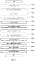
- FIG. 2 is a flowchart of an exemplary procedure of a first operation of SPFS apparatus 100.
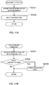
- FIG. 3 is a flowchart of steps in a step of adjusting the position and the output (step S120) illustrated in FIG. 2 .
- an abnormality detection step step S1202 is included in the step of adjusting the position and the output (step S120).
- analysis chip 10 is installed at an installation position of SPFS apparatus 100 (step S100). To be more specific, analysis chip 10 is installed in chip holder 154 of SPFS apparatus 100.
- control processing section 160 operates conveyance stage 152 to move analysis chip 10 to a liquid feeding position (step S105).
- control processing section 160 operates liquid feeding unit 140 to introduce the sample solution in chemical liquid chip 141 into channel 41 of analysis chip 10 (step S110).
- channel 41 the detection object substance is captured on metal film 30 by an antigen-antibody reaction (primary reaction).
- the sample solution in channel 41 is removed, and the interior of channel 41 is washed with the washing solution. It is to be noted that when moisturizing agent is present in channel 41 of analysis chip 10, the interior of channel 41 is washed prior to the introduction of the sample solution to remove the moisturizing agent so that the capturing body can properly capture the detection object substance.
- control processing section 160 operates conveyance stage 152 to move analysis chip 10 to a position near the measurement position (step S115).
- control processing section 160 operates excitation light irradiating unit 110, excitation light detecting unit 120 and conveyance stage 152 to acquire the position information of analysis chip 10 and the output information of excitation light irradiating unit 110.
- Control processing section 160 adjusts the position of analysis chip 10 on the basis of the acquired position information.
- control processing section 160 determines whether excitation light irradiating unit 110 is in a normal condition on the basis of the acquired output information. Then, when it is determined that the power of excitation light irradiating unit 110 is abnormal, control processing section 160 adjusts the power of excitation light irradiating unit 110 on the basis of the acquired output information (step S120).
- step S1201 analysis chip 10 held by chip holder 154 is irradiated with excitation light ⁇ , and reflection light ⁇ of excitation light ⁇ reflected by the surface of analysis chip 10 is detected, thereby acquiring the position information of analysis chip 10 and the output information of excitation light irradiating unit 110 (information relating to the power) (step S1201).
- control processing section 160 determines whether the power of excitation light irradiating unit 110 (i.e. light source unit 111) is normal (step S1202).
- information relating to the power of excitation light irradiating unit 110 of the initial state is stored.
- the intensity of reflection light ⁇ , from the surface of analysis chip 10, of excitation light ⁇ emitted from excitation light irradiating unit 110 of the initial state (hereinafter referred to as simply as "initial value”) is stored.
- Control processing section 160 compares the detection value of reflection light ⁇ detected in step S121 with the initial value preliminarily stored in control processing section 160 to determine whether the power of excitation light irradiating unit 110 is normal. For example, the difference between the initial value and the detection value is greater than a predetermined reference value (threshold), control processing section 160 determines that the power of excitation light irradiating unit 110 is abnormal.
- the reference value (threshold) is appropriately set in accordance with the accuracy required for the analysis.
- control processing section 160 adjusts the output of excitation light irradiating unit 110 to a desired power (step S1203).
- control processing section 160 continues the subsequent operations.
- control processing section 160 adjusts the position of analysis chip 10 (step S1204).
- control processing section 160 can specify the degree of the positional displacement of analysis chip 10 from the measurement position on the basis of the position information.
- control processing section 160 operates conveyance stage 152 to move chip holder 154, and dispose analysis chip 10 at an appropriate measurement position.
- FIGS. 4A and 4B are schematic views for describing a step of acquiring the position information of analysis chip 10 and the output information of excitation light irradiating unit 110 (step S1201).
- step S1201 First, as illustrated in FIG. 4A , in the case where analysis chip 10 is located at a position remote from light source unit 111, when light source unit 111 emits excitation light ⁇ , the excitation light ⁇ is reflected by channel closure 40 and travels toward the lower side (conveyance stage 152 side). Thus, reflection light ⁇ from the surface of analysis chip 10 is not incident on first light receiving sensor 121 of excitation light detecting unit 120.
- excitation light ⁇ from light source unit 111 reaches the boundary (hereinafter referred to as "edge") between prism 20 and channel closure 40.
- edge the boundary between prism 20 and channel closure 40.
- excitation light ⁇ (reflection light ⁇ ) reflected by channel closure 40 does not enter first light receiving sensor 121
- excitation light ⁇ (reflection light ⁇ ) reflected by incidence surface 21 enters first light receiving sensor 121.
- a part of reflection light ⁇ from analysis chip 10 enters first light receiving sensor 121.
- FIGS. 5A and 5B are graphs showing examples of detection results of reflection light ⁇ by first light receiving sensor 121.
- the intensity of reflection light ⁇ was measured with first light receiving sensor 121 while moving analysis chip 10 by conveyance stage 152 in one direction (x-axis direction) in units of 100 ⁇ m.
- the beam diameter of excitation light ⁇ is approximately 1 to 1.5 mm.
- FIG. 5A shows only detection results, and FIG. 5B shows also three approximation lines.
- the intensity of reflection light ⁇ incident on first light receiving sensor 121 is almost constant and maximized.
- the reason for this is that the entirety of reflection light ⁇ enters first light receiving sensor 121 (see FIG. 4C ).
- the inclined part (moving distance: approximately 1,000 ⁇ m to approximately 2,000 ⁇ m) in the graph corresponds to the edge.
- the width of the inclined part corresponds to the beam diameter (approximately 1 mm to approximately 1.5 mm) of excitation light ⁇ in the x-axis direction.
- the horizontal part in the former half (moving distance: 0 to approximately 1,000 ⁇ m), the inclined part (moving distance: approximately 1,000 ⁇ m to approximately 2,000 ⁇ m), and the horizontal part in the latter half (moving distance: greater than approximately 2,000 ⁇ m) are each approximated by a straight line.
- point A is the intersection of the approximation straight line of the horizontal part in the former half and the approximation straight line of the inclined part.
- Point B is the intersection of the approximation straight line of the inclined part and the approximation straight line of the horizontal part in the latter half.
- Point C is the middle point between point A and point B.
- Point A corresponds to a minimum value of the intensity of reflection light ⁇ .
- Point B corresponds to a maximum value of the intensity of reflection light ⁇ .
- Point C corresponds to an intermediate value of the intensity of reflection light ⁇ .
- points A to C may be used to specify the position of analysis chip 10.
- Point A and point B indicate points where the end of the beam of excitation light ⁇ reaches the edge. Accordingly, the position of the edge can be specified by considering the beam diameter of excitation light ⁇ , and as a result, the position of analysis chip 10 can be specified.
- point C indicates a point where the center of the beam of excitation light ⁇ reaches the edge.
- point C is utilized, the position of the edge can be specified without considering the beam diameter of excitation light ⁇ , and as a result, the position of analysis chip 10 can be specified. Accordingly, from the viewpoint of suppressing the influence of the beam diameter of excitation light ⁇ , it is preferable to use the intermediate value of the intensity of reflection light ⁇ of excitation light ⁇ for specifying the position of analysis chip 10.
- point B may be used to acquire information relating to the power of excitation light irradiating unit 110.
- Point B is a maximum value of the intensity of reflection light ⁇ of excitation light ⁇ emitted from excitation light irradiating unit 110, and is an output value of excitation light ⁇ emitted from irradiation light irradiating unit 110. Accordingly, by comparing the initial value and the maximum value of the intensity of reflection light ⁇ , whether the power of excitation light irradiating unit 110 (light source unit 111) is lowered can be determined.
- the position of analysis chip 10 can be specified by irradiating analysis chip 10 with excitation light ⁇ , and detecting reflection light ⁇ of excitation light ⁇ reflected by the surface of analysis chip 10.
- first light receiving sensor 121 is disposed at a position where reflection light ⁇ from channel closure 40 reached but reflection light ⁇ from incidence surface 2 does not reach as illustrated in FIG. 6A , an effect similar to those of the exemplary cases illustrated in FIGS. 4A to 4C is achieved (the intensity of reflection light ⁇ is high when the moving distance is short, and the intensity of reflection light ⁇ is low when the moving distance is long).
- incidence surface 21 since the position of incidence surface 21 is an important factor, it is preferable to irradiate incidence surface 21 and a surface adjacent to incidence surface 21 (in the present embodiment, the rear surface of channel closure 40) of analysis chip 10 with excitation light ⁇ when two adjacent surfaces of analysis chip 10 are irradiated with excitation light ⁇ . Then, incidence surface 21 of prism 20 and the bottom surface of prism 20 may be irradiated with excitation light ⁇ as illustrated in FIG. 6B . In the example illustrated in FIG. 6B , however, analysis chip 10 is closer to light source unit 111 relative to the measurement position at the time of specifying the position of analysis chip 10 (step S120).
- chip holder 154 is required to be moved in an opposite direction by conveyance stage 152 when moving analysis chip 10 to the measurement position (step S142).
- This operation of conveyance stage 152 in two directions might lead to reduction in operation accuracy in comparison with the case where conveyance stage 152 is operated in only one direction.
- chip holder 154 is not required to be moved in opposite directions by conveyance stage 152 in the exemplary cases illustrated in FIGS. 4A to 4C and FIG. 6A .
- step S1201 it is preferable to move chip holder 154 by conveyance stage 152 only in a direction (x-axis direction) toward the light source of excitation light ⁇ (light source unit 111) in the step of acquiring the position information of analysis chip 10 (step S1201) and the step of moving the analysis chip to the measurement position (step S1204).
- the "two adjacent surfaces of analysis chip 10" include two substantially adjacent surfaces.
- analysis chip 10' including prism 20, metal film 30 disposed on film formation surface 22 of the prism, spacer 42 disposed on metal film 30, and channel closure 40 disposed on spacer 42 is used as illustrated in FIG. 7 .
- the shape of channel 41 is defined by spacer 42, and channel closure 40 is a transparent flat plate. Strictly speaking, in this case, since the side surface of spacer 42 extends between incidence surface 21 of prism 20 and the bottom surface of channel closure 40, incidence surface 21 and the bottom surface of channel closure 40 are not adjacent to each other.
- incidence surface 21 and the bottom surface of channel closure 40 can be considered to be substantially adjacent to each other. Accordingly, in this case, reflection light ⁇ from incidence surface 21 and the bottom surface of channel closure 40 that are substantially adjacent to each other is detected to detect the edge.
- joining members such as adhesive agent and a double-sided tape, metal film 30, and the like are also negligible.
- the thickness of the above-mentioned members (for example, spacer 42) that are negligible in detection of reflection light ⁇ is equal to or smaller than 1/5 of the beam diameter of excitation light ⁇ , preferably, equal to or smaller than 1/10 of the beam diameter of excitation light ⁇ .
- the most part of (4/5 or more, or 9/10 or more) of reflection light ⁇ from the surface of analysis chip 10' is reflection light ⁇ from incidence surface 21 or the bottom surface of channel closure 40, and is utilized for the position detection.
- the position of analysis chip 10' can be specified without being influenced by spacer 42.
- a member such as spacer 42, a joining member and metal film 30
- whose thickness is equal to or smaller than 1/5 of the beam diameter of excitation light ⁇ is negligible in detection of reflection light ⁇ . That is, incidence surface 21 and the bottom surface of channel closure 40 of analysis chip 10' can be regarded as two substantially adjacent surfaces.
- FIGS. 8A and 8B are schematic views for describing a step (step S1204) of disposing analysis chip 10 to an appropriate measurement position.
- step S1204 the position of the edge is specified as illustrated in FIG. 8A .
- the distance between the position of the edge and the region to which excitation light ⁇ should be applied in the rear surface of metal film 30 (the region on the rear side of the reaction site) is determined.
- FIG. 8B by controlling conveyance stage 152 to move chip holder 154 by a predetermined distance, analysis chip 10 can be disposed at an appropriate measurement position.
- analysis chip 10 can be disposed at an appropriate measurement position.
- a case is assumed in which the position of the edge is specified as illustrated in FIG. 9A .
- the position of analysis chip 10 is shifted in the x-axis direction in comparison with the case (indicated with the broken line in the drawing) where analysis chip 10 is not shifted in the z-axis direction.
- analysis chip 10 can be disposed at an appropriate measurement position by moving chip holder 154 by a predetermined distance by conveyance stage 152 on the basis of the position of the edge.
- control processing section 160 operates excitation light irradiating unit 110 and fluorescence detecting unit 130 to irradiate analysis chip 10 disposed at an appropriate measurement position with excitation light ⁇ , and detects plasmon scattering light ⁇ whose wavelength is identical to that of excitation light ⁇ , thereby detecting the enhancement angle (step S125).
- control processing section 160 operates excitation light irradiating unit 110 to scan the incident angle of excitation light ⁇ to metal film 30, while operating fluorescence detecting unit 130 to detect plasmon scattering light ⁇ .
- control processing section 160 operates position switching mechanism 132 to dispose optical filter 135 at a position outside the light path of light receiving unit 131. Then, control processing section 160 determines, to be the enhancement angle, the incident angle of excitation light ⁇ at which the quantity of the plasmon scattering light ⁇ is maximized.
- control processing section 160 operates excitation light irradiating unit 110 and fluorescence detecting unit 130 to irradiate analysis chip 10 disposed at an appropriate measurement position with excitation light ⁇ , and records an output value (optical blank value) of second light receiving sensor 137 (step S130).
- control processing section 160 operates angle adjusting mechanism 112 to set the incident angle of excitation light ⁇ to the enhancement angle.
- control processing section 160 controls position switching mechanism 132 to dispose optical filter 135 at a position on the light path of light receiving unit 131.
- control processing section 160 operates conveyance stage 152 to move analysis chip 10 to a liquid feeding position (step S135).
- control processing section 160 operates liquid feeding unit 140 to introduce liquid (labeling solution) containing a secondary antibody labeled with a fluorescence material into channel 41 of analysis chip 10 (step S140).
- liquid (labeling solution) containing a secondary antibody labeled with a fluorescence material into channel 41 of analysis chip 10
- an antigen-antibody reaction secondary reaction
- a detection object substance captured on metal film 30 is labeled with the fluorescence material.
- the labeling solution in channel 41 is removed, and the interior of the channel is washed with washing solution.
- control processing section 160 operates conveyance stage 152 to move analysis chip 10 to an appropriate measurement position determined in step S120 (step S145).
- control processing section 160 operates excitation light irradiating unit 110 and fluorescence detecting unit 130 to irradiate analysis chip 10 disposed at an appropriate measurement position with excitation light ⁇ , and detects fluorescence ⁇ emitted from the fluorescence material labelling the detection object substance captured by the capturing body (step S150).
- control processing section 160 subtracts the optical blank value from the detection value of fluorescence ⁇ to calculate the intensity of the fluorescence correlating with the amount of the detection object substance (step S155).
- the intensity of the calculated fluorescence is converted to the amount, the concentration, and the like of the detection object substance as necessary.
- the presence or the amount of the detection object substance in the sample solution can be detected.
- SPFS apparatus 100 acquires information relating to the power of excitation light irradiating unit 110 as the output information of excitation light irradiating unit 110.
- SPFS apparatus 100 corrects the detection value of fluorescence ⁇ in accordance with the value of the power of excitation light irradiating unit 110.
- FIG. 10 is a flowchart of an exemplary procedure of the second operation of SPFS apparatus 100.
- FIG. 11A is a flowchart of steps in the position adjustment step (step S220) illustrated in FIG. 10
- FIG. 11B is a flowchart of steps in the step of calculating the fluorescence intensity correlating with the amount of the detection object substance (step S255) illustrated in FIG. 10 .
- an abnormality detection step step S2552 is included in the step of calculating the amount of the detection object substance and the like (step S255).
- analysis chip 10 is installed at an installation position of SPFS apparatus 100 (step S200). To be more specific, analysis chip 10 is installed in chip holder 154 of SPFS apparatus 100.
- control processing section 160 operates conveyance stage 152 to move analysis chip 10 to a liquid feeding position (step S205).
- control processing section 160 operates liquid feeding unit 140 to introduce the sample solution in chemical liquid chip 141 into channel 41 of analysis chip 10 (step S210).
- channel 41 a detection object substance is captured on metal film 30 by an antigen-antibody reaction (primary reaction). Thereafter, the sample solution in channel 41 is removed, and the interior of channel 41 is washed with the washing solution. It is to be noted that when moisturizing agent is present in channel 41 of analysis chip 10, the interior of channel 41 is washed prior to the introduction of the sample solution to remove the moisturizing agent so that the capturing body can appropriately capture the detection object substance.
- control processing section 160 operates conveyance stage 152 to move analysis chip 10 to a position near the measurement position (step S215).
- control processing section 160 operates excitation light irradiating unit 110, excitation light detecting unit 120 and conveyance stage 152 to acquire the position information of analysis chip 10 and the output information of excitation light irradiating unit 110. On the basis of the acquired position information, control processing section 160 adjusts the position of analysis chip 10 (step S220).
- step S2201 analysis chip 10 held by chip holder 154 is irradiated with excitation light ⁇ , and reflection light ⁇ of excitation light ⁇ reflected by the surface of analysis chip 10 is detected, thereby acquiring the position information of analysis chip 10 and the output information of excitation light irradiating unit 110 (information relating to the power) (step S2201).
- the output information acquired at this time is recorded in control processing section 160.
- control processing section 160 adjusts the position of analysis chip 10 (step S2202).
- the step of acquiring the position information of analysis chip 10 and the output information of excitation light irradiating unit 110 (step S2201) is similar to step S1201, and the step of disposing analysis chip 10 at an appropriate measurement position on the basis of the acquired position information (step S2202) is similar to step S1204, and therefore, the descriptions thereof will be omitted.
- control processing section 160 detects the enhancement angle as in step S125 (step S225).
- control processing section 160 measures and records the optical blank value as in step S130 (step S230).
- control processing section 160 operates conveyance stage 152 to move analysis chip 10 to a liquid feeding position (step S235).
- control processing section 160 labels the detection object substance captured on metal film 30 with the fluorescence material as in step S140 (step S240).
- control processing section 160 operates conveyance stage 152 to move analysis chip 10 to an appropriate measurement position determined in step S220 (step S245).
- control processing section 160 detects fluorescence ⁇ emitted from the fluorescence material labelling the detection object substance captured by the capturing body as in step S150 (step S250).
- control processing section 160 calculates the amount, the concentration and the like of the detection object substance (step S255).
- the optical blank value is subtracted from the detection value of fluorescence ⁇ , and the fluorescence intensity correlating with the amount of the detection object substance is calculated (step S2551).
- control processing section 160 determines whether the power of excitation light irradiating unit 110 is normal (step S2552).
- the detection value of reflection light ⁇ detected in step S2201 and the initial value of reflection light ⁇ are stored.
- Control processing section 160 compares the detection value and the initial value to determine whether the power of excitation light irradiating unit 110 is normal.
- control processing section 160 corrects the fluorescence intensity calculated in step S2551 (step S2553).
- control processing section 160 calculates the degree of the reduction of the power of excitation light irradiating unit 110, and multiplies the fluorescence intensity calculated in step S2551 by a correction coefficient (for example, 100/70 when the power of excitation light irradiating unit 110 is lowered to 70%) configured to make up the power reduction. In this manner, control processing section 160 corrects the calculated fluorescence intensity.
- the corrected fluorescence intensity is converted to the amount, the concentration, and the like of the detection object substance as necessary.
- the presence or the amount of the detection object substance in the sample solution can be detected.
- the surface plasmon resonance fluorescence analysis method and the surface plasmon resonance fluorescence analysis apparatus (SPFS apparatus 100) can acquire the output information (information relating to the power) of excitation light irradiating unit 110 by detecting reflection light ⁇ of excitation light ⁇ .
- Reflection light ⁇ that is reflected at the surface (in the present embodiment, incidence surface 21) of analysis chip 10 is approximately several percent of excitation light ⁇ from excitation light irradiating unit 110, and therefore first light receiving sensor 121 is not saturated.
- the analysis method and SPFS apparatus 100 can correctly determine whether excitation light irradiating unit 110 is in a normal condition, and can prevent detection errors due to abnormality in excitation light irradiating unit 110, without separately using a light quantity adjustment means.
- the task and the cost for maintenance such as replacing and cleaning of a light quantity adjusting component can be reduced.
- analysis chip 10 is replaced for each analysis and excitation light ⁇ from excitation light irradiating unit 110 is always reflected by a clean surface, there is no influence of the aging of the reflecting surface, dust, and the like. Also in view of this, it is possible to correctly determine whether excitation light irradiating unit 110 is in a normal condition.
- an SPFS apparatus that can acquire information relating to the power of excitation light irradiating unit 110 and the irradiation direction of excitation light ⁇ as output information of the excitation light irradiating unit (excitation light irradiating section) is described.
- SPFS apparatus 200 is different from SPFS apparatus 100 according to the previously described example only in configuration of first light receiving sensor 221 of excitation light detecting unit 220.
- first light receiving sensor 221 in SPFS apparatus 200 is described below, and the components identical to those of SPFS apparatus 100 according to the previously described example are denoted with the same reference numerals, and, the description thereof will be omitted.
- analysis chip 10 used in SPFS apparatus 200 according to the invention is identical to analysis chip 10 used in SPFS apparatus 100 according to the previously described example, and therefore the description thereof will be omitted.
- FIG. 1 is a schematic view illustrating a configuration of a surface plasmon resonance fluorescence analysis apparatus (SPFS apparatus) 100 according to the present invention.
- SPFS apparatus 100 includes excitation light irradiating unit (excitation light irradiating section) 110, excitation light detecting unit (excitation light detecting section) 220, fluorescence detecting unit (fluorescence detecting section) 130, liquid feeding unit 140, conveyance unit 150 and control processing section (processing section) 160.
- Excitation light detecting unit 220 includes first light receiving sensor 221 and first sensor controlling section 122.
- First light receiving sensor 221 detects the quantity and the position of reflection light ⁇ .
- light receiving sensor 221 is a position detection device (PSD) or a photodiode (PD) including a plurality of light reception surfaces.
- PSD position detection device
- PD photodiode
- the number of the light reception surfaces of first light receiving sensor 221 is preferably, but not limited to, four or more.
- first light receiving sensor 221 is a PD including four light reception surfaces.
- first light receiving sensor 221 is a PSD
- the size of the light reception surface of first light receiving sensor 221 is set to a size greater than the beam diameter of excitation light ⁇ from the viewpoint of correctly detecting the irradiation position of excitation light ⁇ .
- the length of one side of the light reception surface of first light receiving sensor 221 is preferably 3 mm or greater.
- First light receiving sensor 221 is disposed at a position where reflection light ⁇ of excitation light ⁇ reaches.
- first light receiving sensor 221 is disposed at a position where reflection light ⁇ from incidence surface 21 reaches.
- first light receiving sensor 221 is disposed at a position where reflection light ⁇ of excitation light ⁇ emitted at an angle for the detection of fluorescence ⁇ or an angle approximately equal to the angle for the detection of fluorescence ⁇ reaches.
- the irradiation position of excitation light ⁇ slightly varies depending on variation of the incident angle, and therefore, by setting the incident angle of excitation light ⁇ for positioning of analysis chip 10 and the incident angle of excitation light ⁇ for detection of fluorescence ⁇ to values equal to or approximately equal to each other, the accuracy of positioning at the time of detection of fluorescence ⁇ can be enhanced.
- the emission angle of excitation light ⁇ to the normal of metal film 30 (straight line along the z-axis direction in FIG. 1 ) is approximately 70 degrees
- reflection light ⁇ from incidence surface 21 advances in a direction approximately parallel to the travelling direction of the conveyance stage (x-axis direction in FIG. 1 ). Accordingly, first light receiving sensor 221 is disposed at a position where the reflection light ⁇ that travels in parallel reaches.
- SPFS apparatus 200 acquires information relating to the power of excitation light irradiating unit 110 and the irradiation direction of excitation light ⁇ as output information of excitation light irradiating unit 110. Then, when it is determined that the power of excitation light irradiating unit 110 is abnormal, SPFS apparatus 200 adjusts the power of excitation light irradiating unit 110. In addition, when it is determined that the irradiation direction of excitation light ⁇ is abnormal, excitation light irradiating unit 110 stops the subsequent operations.
- FIG. 12 is a flowchart of an exemplary procedure of an operation of SPFS apparatus 200.
- FIG. 13 is a flowchart of steps in the step of adjusting the position and the output illustrated in FIG. 12 (step S320).
- the abnormality detection step (step S3202 and step S3203) is included in the step of adjusting the position and the output (step S320).
- analysis chip 10 is installed at an installation position of SPFS apparatus 200 (step S300). To be more specific, analysis chip 10 is installed in chip holder 154 of SPFS apparatus 200.
- control processing section 160 operates conveyance stage 152 to move analysis chip 10 to a liquid feeding position (step S305).
- control processing section 160 operates liquid feeding unit 140 to introduce the sample solution in chemical liquid chip 141 into channel 41 of analysis chip 10 (step S310).
- channel 41 a detection object substance is captured on metal film 30 by an antigen-antibody reaction (primary reaction). Thereafter, the sample solution in channel 41 is removed, and the interior of channel 41 is washed with the washing solution. It is to be noted that when moisturizing agent is present in channel 41 of analysis chip 10, the interior of channel 41 is washed prior to the introduction of the sample solution to remove the moisturizing agent so that the capturing body can appropriately capture the detection object substance.
- control processing section 160 operates conveyance stage 152 to move analysis chip 10 to a position near the measurement position (step S315).
- control processing section 160 operates excitation light irradiating unit 110, excitation light detecting unit 220 and conveyance stage 152 to acquire the position information of analysis chip 10 and the output information of excitation light irradiating unit 110.
- Control processing section 160 adjusts the position of analysis chip 10 on the basis of the acquired position information, and adjusts the output of excitation light irradiating unit 110 on the basis of the acquired output information (step S320).
- control processing section 160 stops the subsequent steps.
- control processing section 160 determines whether the irradiation direction of excitation light ⁇ from excitation light irradiating unit 110 is normal (step S3202).
- information relating to the irradiation direction of excitation light ⁇ of excitation light irradiating unit 110 in the initial state is stored.
- information relating to the irradiation position of reflection light ⁇ with respect to first light receiving sensor 221 (hereinafter referred to also simply as "initial position") is stored.
- control processing section 160 compares the position of the irradiation spot on first light receiving sensor 221 of reflection light ⁇ detected in step S3201 with the initial position preliminarily stored in control processing section 160 to determine whether the irradiation direction of excitation light ⁇ from excitation light irradiating unit 110 is normal.
- control processing section 160 When it is determined that the irradiation direction of excitation light ⁇ is normal, control processing section 160 continues the subsequent operations, whereas when it is determined that the irradiation direction of excitation light ⁇ is shifted from the desired direction (abnormal), control processing section 160 terminates the operation.
- step S3203 The step of detecting abnormality in the power (step S3203), the step of adjusting the power of excitation light irradiating unit 110 (step S3204), the step of disposing analysis chip 10 at an appropriate measurement position on the basis of the position information of analysis chip 10 (step S3205) are respectively similar to steps S1202 to S1204 of the previously described example, and therefore the descriptions thereof will be omitted.
- FIG. 14 is a schematic view for describing the step (step S3201) of acquiring the output information of excitation light irradiating unit 110 (information relating to the power and the irradiation direction of excitation light ⁇ ) in the case where a PD including four light reception surfaces is used.
- the dotted area indicates an irradiation spot of excitation light ⁇ applied to light reception surfaces 221a to 221d of first light receiving sensor 221.
- first light receiving sensor 221 is a PD including four light reception surfaces, 221a to 221d.
- photoelectric currents I a to I d corresponding to the quantity of applied reflection light ⁇ are generated in light reception surfaces 221a to 221d, respectively.
- the irradiation positions of excitation light ⁇ in light reception surfaces 221a to 221d in the plane direction can be specified.
- control processing section 160 can acquire information relating to the irradiation direction of excitation light ⁇ .
- the irradiation position of reflection light ⁇ in the vertical direction in FIG. 14 can be specified on the basis of the ratio of (I a +I b ):(I c +I d ), and the irradiation positions of reflection light ⁇ in the lateral direction in FIG. 14 can be specified on the basis of the ratio of (I a +I c ):(I b +I d ).
- control processing section 160 photoelectric current values I a to I d output from light reception surfaces 221a to 221d of first light receiving sensor 221 are stored as the initial position, and control processing section 160 can determine whether the irradiation direction of excitation light ⁇ is shifted by comparing photoelectric current values I a to I d measured in step S3201 with preliminarily stored photoelectric current values I a to I d .
- control processing section 160 can measure the intensity of reflection light ⁇ on the basis of the sum (I a +I b +I c +I d ) of photoelectric currents I a to I d output from light reception surfaces 221a to 221d, and can acquire information relating to the power of excitation light irradiating unit 110.
- Control processing section 160 can determine whether the power of excitation light irradiating unit 110 is lowered by comparing the sum (I a +I b +I c +I d ) of photoelectric currents I a to I d measured in step S3201 with the sum (I a +I b +I c +I d ) of preliminarily stored photoelectric currents I a to I d .
- step S3202 the order of the step of detecting abnormality in the irradiation direction of excitation light ⁇ (step S3202) and the step of detecting abnormality in the power of excitation light irradiating unit 110 (step S3203) is not limited to the above-mentioned order, and the step of detecting abnormality in the irradiation direction of excitation light ⁇ (step S3202) may be performed after the step of detecting abnormality in the power (step S3203).
- the output information of excitation light irradiating unit 110 (information relating to power and the irradiation direction of excitation light ⁇ ) can be acquired.
- a PD including a plurality of divided light reception surfaces reflection light ⁇ incident on a region between adjacent light reception surfaces (region where excitation light ⁇ is not received) is not detected, and consequently the quantity of reflection light ⁇ cannot be wholly detected.
- the quantity of reflection light ⁇ can be wholly detected since the light reception surface of a PSD is one continuous surface. It is therefore preferable to use a PSD as first light receiving sensor 221 from the viewpoint of more correctly detecting the quantity of reflection light ⁇ .
- control processing section 160 detects the enhancement angle as in step S125 (step S325).
- control processing section 160 measures and records the optical blank value as in step S130 (step S330).
- control processing section 160 operates conveyance stage 152 to move analysis chip 10 to a liquid feeding position (step S335).
- control processing section 160 labels the detection object substance captured on metal film 30 with the fluorescence material as in step S140 (step S340).
- control processing section 160 operates conveyance stage 152 to move analysis chip 10 to an appropriate measurement position determined in step S320 (step S345).
- control processing section 160 detects fluorescence ⁇ emitted from the fluorescence material labelling the detection object substance captured by the capturing body as in step S150 (step S350).
- control processing section 160 subtracts the optical blank value from the detection value of fluorescence ⁇ to calculate the fluorescence intensity correlating with the amount of the detection object substance (step S355).
- the intensity of the detected fluorescence is converted to the amount, the concentration, and the like of the detection object substance as necessary.
- the presence or the amount of the detection object substance in the sample solution can be detected.
- the analysis method and the SPFS apparatus according to the invention can detect abnormality in the irradiation direction of excitation light ⁇ from excitation light irradiating unit 110 while achieving the effect of the previously described example.
- FIG. 15 is a graph for describing another method for acquiring information relating to the power of the excitation light irradiating unit, in which the information relating to the power of excitation light irradiating unit 110 is acquired on the basis of the inclination of a straight line between point A and point C (a ratio of a variation of a reflection light intensity to a variation of a moving distance of analysis chip 10) instead of the point B in FIG. 5B .
- control processing section 160 the inclination of the straight line between point A and point C is stored as the information relating to the power of excitation light irradiating unit 110.
- the black circle ( ⁇ ) indicates a detection result of reflection light by the first light receiving sensor in the case where excitation light irradiating unit 110 of the initial state is used
- the white circle ( ⁇ ) indicates a detection result of reflection light by the first light receiving sensor in the case where excitation light irradiating unit 110 in a low power state is used.
- a result of the case where the power of excitation light irradiating unit 110 is lowered to 1/2 of the power of the initial state is illustrated. As illustrated in FIG.
- the maximum value of reflection light ⁇ obtained with excitation light irradiating unit 110 in a low power state is halved.
- the inclination of the inclined part (moving distance: approximately 2320 to approximately 2380 ⁇ m) is also halved.
- the information relating to the power of excitation light irradiating unit 110 can be acquired also on the basis of a ratio of a variation of a reflection light intensity to a variation of a moving distance of analysis chip 10.
- the position of analysis chip 10 may be adjusted before the power of excitation light irradiating unit 110 is adjusted, or after the power of excitation light irradiating unit 110 is adjusted, or, while the power of excitation light irradiating unit 110 is adjusted.
- the enhancement angle may be detected (steps S125, S225, S325) before the primary reaction (steps S110, S210, S310).
- the adjustment of the position (position and output) (steps S120, S220, S320) is also performed before the primary reaction (steps S110, S210, S310).
- step S105, S205, S305 the positional accuracy in the step of moving analysis chip 10 to the liquid feeding position prior to the primary reaction (steps S120, S220, S320) is enhanced, and, in the primary reaction (steps S120, S220, S320) and the secondary reaction (steps S140, S240, S340), an end of syringe 144 of liquid feeding unit 140 can be more surely inserted into analysis chip 10.
- step S100, S200, S300 thus improving usability.
- the timing when the detection object substance is labeled with the fluorescence material is not limited.
- the labeling solution may be added to the sample solution to preliminarily label the detection object substance with the fluorescence material before the sample solution is introduced into the channel of analysis chip 10.
- the sample solution and the labeling solution may be simultaneously injected into the channel of analysis chip 10.
- both the primary reaction and the secondary reaction can be completed (one step method).
- the detection of the enhancement angle step S125, S225, S325
- the adjustment of the position is performed (steps S120, S220, S320) before the detection of the enhancement angle.
- the surface plasmon resonance fluorescence analysis method and the surface plasmon resonance fluorescence analysis apparatus are not limited to this.
- the surface plasmon resonance fluorescence analysis method and the surface plasmon resonance fluorescence analysis apparatus according to the embodiments of present invention may be used only for acquiring the output information.
- FIGS. 16A and 16B are graphs showing a relationship between the incident angle and the reflectivity of excitation light.
- FIG. 16A shows a result of the case where excitation light hits the surface of the prism from the outside of the prism
- FIG. 16B shows a result of the case where excitation light hits the surface of the prism from the inside of the prism.
- the solid line indicates p-polarized light
- the broken line indicates s-polarized light.
- the relationship between the refractive index of the prism and the reflectivity of p-polarized light of excitation light was calculated.
- the incident angle of the excitation light to the incidence surface was set to 9 degrees (0.158 rad) such that the incident angle to the metal film is 71 degrees.
- the reflectivity of the excitation light in the case where the refractive index is varied by ⁇ 0.002 from the reference refractive index, and the reflectivity of the excitation light in the case where the refractive index is varied by ⁇ 0.003 from the reference refractive index were calculated. Results of the calculation are shown in Table 1.
- the refractive index variation is a variation in refractive index with respect to the reference refractive index 1.527.
- the change rate of reflectivity [%] is a change rate with respect to a reference reflectivity obtained with a prism having a refractive index of 1.527.
- [Table 1] Refractive index Refractive index variation Reflectivity of p-polarized light [%] Change rate of reflectivity [%] 1.527 0 4.2067 0 1.529 +0.002 4.2322 +0.61 1.525 -0.002 4.1813 -0.61 1.530 +0.003 4.2450 +0.91 1.524 -0.003 4.1686 -0.91
- the reflectivity of the p-polarized light of the excitation light was approximately 4.2%.
- the variation of the refractive index was ⁇ 0.002
- the change rate of the reflectivity was approximately ⁇ 0.61%
- the variation of the refractive index was ⁇ 0.003
- the change rate of the reflectivity was approximately ⁇ 0.91%. That is, it was confirmed that as long as the variation of the refractive index is approximately ⁇ 0.003, the change rate of the reflectivity is 1% or lower and the reflectivity is substantially constant.
- abnormality in the power can be correctly detected by detecting reflection light of excitation light from the prism so as to acquire information relating to the power of the excitation light irradiating unit since, when the incident angle of the excitation light to the prism is small, the reflectivity of the excitation light is substantially constant as long as the prism is made of the same material.
- the surface plasmon resonance fluorescence analysis method and the surface plasmon resonance fluorescence analysis apparatus according to the embodiments of the present invention can detect a detection object substance with high reliability, and therefore is suitable for laboratory test and the like, for example.
Description
- The present invention relates to a surface plasmon resonance fluorescence analysis method and a surface plasmon resonance fluorescence analysis apparatus that detect a detection object substance in a sample solution with use of surface plasmon resonance (SPR).
- When trace substances can be quantitatively detected with high sensitivity in measurement for detection of biological substances such as protein and DNA, determination of the patient's condition and treatment can be promptly carried out. In view of this, an analysis method and an analysis apparatus for quantitatively detecting weak light generated by a very small amount detection object substance with high sensitivity are demanded. As an example of a method of detecting a detection object substance with high sensitivity, a surface plasmon resonance fluorescence analysis method (Surface Plasmon-field enhanced Fluorescence Spectroscopy (SPFS)) is known (see, for example, PTL 1).
- The SPFS uses a prism including a metal film disposed on a predetermined surface. When the metal film is irradiated with excitation light from an excitation light irradiating section through the prism at an angle that causes a surface plasmon resonance, localized light (enhanced electric field) can be generated on the surface of the metal film. With the localized light, a fluorescence material labelling the detection object substance captured on the metal film is excited, and therefore the presence or the amount of the detection object substance can be detected by detecting the fluorescence emitted from the fluorescence material.
- PTL 1
WO2012/172987 -
WO 2015/064704 A1 discloses that excitation light is irradiated onto an analysis chip that has been placed in a chip holder, reflected light or transmitted light from the analysis chip is detected, and as a result the position information of the analysis chip is obtained. On the basis of this position information, the chip holder is moved by a conveyance stage and thereby moved to a measurement position. Excitation light is irradiated onto the analysis chip that is disposed at the measurement position, and fluorescence emitted from a fluorescent substance that marks the substance to be detected is detected. -
JP 2012 098256 A -
WO 2013/027544 A1 discloses that an illumination mechanism radiates excitation light at a prism. A measurement mechanism measures the amount of surface plasmon excitation fluorescence radiated from an antigen trapping film. A duct is formed at a duct-forming body. The antigen trapping film is affixed to the first primary surface of a gold film, and a gold film is adhered to the second primary surface of the gold film. The antigen trapping film is exposed within the duct, and traps antigens. The prism is molded from a resin. The refractive index of the prism is at least 1.5. The photoelastic coefficient of the prism is no greater than 5x10-12 Pa-1. When excitation light is radiated to the prism and a sample liquid containing a quantity of antigens that is the lower limit of detection is filling the duct, the amount of autofluorescence radiated from the prism is less than the amount of surface plasmon excitation fluorescence radiated from the antigen trapping film. -
WO 2006/047192 A1 discloses that a system for measuring light absorption levels for a liquid for use in a printing system includes a light source adapted to provide a divergent beam of light, a liquid container with a hole that acts as a focusing lens, and a prism disposed over the hole to split the divergent beam of light into a reference beam and a measurement beam. The systems include a measurement detector to measure the intensity of the focused beam to produce a liquid measurement signal. A reference detector measures the intensity of the reference beam for compensating the effects of temperature and light source variations on the system signals. A device calculates signal ratios and stores the ratios so that the signal ratios of subsequent colored liquids can be converted into colorant concentrations from a look-up table or through calculations using a signal ratio/colorant concentration. -
US 6 201 607 B1 discloses that light from sources, such as LEDs, is used to detect the levels of glucose and fructosamine in the blood exposed reagent. A special optical arrangement is used to obtain optical signals indicative of the optically sensitive chemicals in the reagent. The optical beams from respective LEDs are directed at a common surface of an optical element used to redirect the light onto the reagent and reflect portions onto a reference detector. A main detector is strategically located adjacent a surface of the optical element to detect reflections from the reagent. A control circuit is described with which the light from the LED light sources can be held at substantially constant levels despite factors tending to cause light level changes. -
JP 2007 047110 A - In general, in an SPFS, the SPFS apparatus is provided with a light receiving sensor for measuring excitation light, and whether the excitation light irradiating section is in a normal condition is checked from the viewpoint of preventing detection errors due to a lowered power of an excitation light irradiating section. In the case where a light receiving sensor (for example, a photodiode (PD)) and a high-power (for example, 1 m W/mm2 or greater) excitation light source are used, when the power of the light source is excessively high, an excessively large quantity of excitation light is detected and consequently the light receiving sensor is saturated in some situation. When the light receiving sensor is saturated in this manner, the linearity of the output of light receiving sensor is lost, and accurate measurement cannot be performed. As a result, whether the excitation light irradiating section is in a normal condition cannot be correctly determined in some situation. In view of this, to prevent the saturation of the light receiving sensor, a light quantity adjustment means such as a neutral density (ND) filter and a light diffusion plate are used together with the light receiving sensor.
- However, the above-mentioned light quantity adjustment means is influenced by aging, dust in the use environment, and the like. Therefore, to perform precise measurement, maintenance of the light quantity adjustment means such as replacing and cleaning of the light quantity adjustment means has to be periodically performed to eliminate the influence.
- An object of the present invention is to provide a surface plasmon resonance fluorescence analysis method and a surface plasmon resonance fluorescence analysis apparatus that can correctly determine whether an excitation light irradiating section is in a normal condition without separately using a light quantity adjustment means in the case where a high-power light source is used.
- Accordingly, there is provided a surface plasmon resonance fluorescence analysis method as set out in independent claim 1 and a surface plasmon resonance fluorescence analysis apparatus as set out in independent claim 7. Advantageous developments are defined in the dependent claims.
- According to the present invention, it is possible to correctly determine whether an excitation light irradiating section is in a normal condition without separately using a light quantity adjustment means in the case where a high-power light source is used, and it is thus possible to prevent detection errors due to abnormality in the excitation light irradiating section. In addition, the task and the cost for maintenance such as replacing and cleaning of a light quantity adjusting component can be reduced.
-
-
FIG. 1 schematically illustrates a configuration of an SPFS apparatus according to the present invention; -
FIG. 2 is a flowchart of an exemplary procedure of a first operation of the SPFS apparatus according to an example useful for understanding the present invention; -
FIG. 3 is a flowchart of steps in a position adjustment step (step S120) illustrated inFIG. 2 ; -
FIGS. 4A to 4C are schematic views for describing a step of acquiring position information of an analysis chip and output information of an excitation light irradiating unit (step S1201); -
FIGS. 5A and 5B are graphs showing exemplary detection results of reflection light by a first light receiving sensor; -
FIGS. 6A and 6B are schematic views for describing a modification of the step of acquiring the position information of the analysis chip and the output information of the excitation light irradiating unit (step S1201); -
FIG. 7 is a sectional view illustrating another exemplary analysis chip; -
FIGS. 8A and 8B are schematic views for describing a step of disposing the analysis chip at a measurement position (step S1204); -
FIGS. 9A and 9B are schematic views for describing the step of disposing the analysis chip at the measurement position (step S1204); -
FIG. 10 is a flowchart of an exemplary procedure of a second operation of the SPFS apparatus according to an example useful for understanding the present invention; -
FIG. 11A is a flowchart of steps in a position adjustment step (step S220) illustrated inFIG. 10 , andFIG. 11B is a flowchart of steps in a calculation and correction step (step S255) illustrated inFIG. 10 ; -
FIG. 12 is a flowchart of an exemplary procedure of an operation of the SPFS apparatus according to the present invention; -
FIG. 13 is a flowchart of steps in a step of adjusting the position and the output (step S320) illustrated inFIG. 12 ; -
FIG. 14 is a schematic view for describing a step of acquiring output information of the excitation light irradiating unit (step S3201) in the case where a PD including four light reception surfaces is used; -
FIG. 15 is a graph for describing another method for acquiring information relating to the power of the excitation light irradiating unit; and -
FIGS. 16A and 16B are graphs showing a relationship between the incident angle and the reflectivity of excitation light. - The present invention is elaborated below with reference to the accompanying drawings.
- In an example useful for understanding the invention, a surface plasmon resonance fluorescence analysis apparatus (SPFS apparatus) that can acquire, as output information of an excitation light irradiating unit (excitation light irradiating section), information relating to the power of the excitation light irradiating unit is described.
-
FIG. 1 is a schematic view illustrating a configuration ofSPFS device 100. As illustrated inFIG. 1 ,SPFS apparatus 100 includes excitation light irradiating unit (excitation light irradiating section) 110, excitation light detecting unit (excitation light detecting section) 120, fluorescence detecting unit (fluorescence detecting section) 130,liquid feeding unit 140,conveyance unit 150 and control processing section (processing section) 160.SPFS device 100 is used in a state whereanalysis chip 10 is attached tochip holder 154 ofconveyance unit 150. For such a configuration,analysis chip 10 is described first, and each component ofSPFS device 100 is described after the description ofanalysis chip 10. -
Analysis chip 10 includesprism 20 includingincidence surface 21,film formation surface 22 andemission surface 23,metal film 30 formed onfilm formation surface 22, andchannel closure 40 disposed onfilm formation surface 22 ormetal film 30. Normally,analysis chip 10 is replaced for each analysis.Analysis chip 10 is preferably a structure with each side of several millimeters to several centimeters, but may be a smaller structure or a larger structure that are not categorized as "chip." -
Prism 20 is a dielectric that is transparent to excitation light α.Prism 20 includesincidence surface 21,film formation surface 22 andemission surface 23.Incidence surface 21 allows a large part of excitation light α from excitationlight irradiating unit 110 to enterprism 20, and reflects a part of excitation light α from excitationlight irradiating unit 110. In excitation light α from excitationlight irradiating unit 110, the proportion in light quantity (reflectivity) of excitation light α that is reflected by incidence surface 21 (hereinafter referred to also as "reflection light β") depends on the refractive index ofprism 20, the refractive index of the gas aroundprism 20, and the incident angle of excitation light α to incidence surface 21 (see the reference experiment described later). Normally,prism 20 is surrounded by air, and accordingly the reflectivity is substantially constant when the same the material ofprism 20 and the same the incident angle of excitation light α are used. For example, when the material ofprism 20 is a resin whose refractive index is 1.4 to 1.6, the reflectivity is approximately 4.2%.Metal film 30 is disposed onfilm formation surface 22. Excitation light α having enteredprism 20 is reflected by the rear surface ofmetal film 30. To be more specific, excitation light α is reflected by an interface (film formation surface 22) betweenprism 20 andmetal film 30.Emission surface 23 is a surface through which excitation light α reflected bymetal film 30 is emitted out ofprism 20. - The shape of
prism 20 is not limited. In the present embodiment, the shape ofprism 20 has a columnar shape whose bottom surface has a trapezoidal shape. The surface corresponding to one leg isincidence surface 21, and the surface corresponding to the other leg isemission surface 23. Preferably, the trapezoid serving as the bottom surface is an isosceles trapezoid. With such a configuration,incidence surface 21 andemission surface 23 are symmetrical, and the S wave component of excitation light α does not easily remain inprism 20. -
Incidence surface 21 is formed such that excitation light α does not return to excitationlight irradiating unit 110. When excitation light α returns to a laser diode (hereinafter also referred to as "LD") in the case where the light source of excitation light α is the LD, the excitation state of the LD is disturbed, and the wavelength and the output of excitation light α are varied. In view of this, the angle ofincidence surface 21 is set within a scanning range around the ideal enhancement angle such that that excitation light α is not perpendicularly incident onincidence surface 21. Here, the "enhancement angle" is an incident angle at which the quantity of scattering light (hereinafter referred to as "plasmon scattering light") δ having a wavelength equal to that of excitation light α emitted upward ofanalysis chip 10 is maximized when the incident angle of excitation light α with respect tometal film 30 is scanned. In the present embodiment, each of the angle betweenincidence surface 21 andfilm formation surface 22 and the angle betweenfilm formation surface 22 andemission surface 23 is approximately 80 degrees. - It is to be noted that the enhancement angle (and the resonance angle in the close vicinity thereof) largely depends on the design of
analysis chip 10. The design factors are the refractive index ofprism 20, the refractive index ofmetal film 30, the film thickness ofmetal film 30, the extinction coefficient ofmetal film 30, the wavelength of excitation light α, and the like. While the enhancement angle and the resonance angle are shifted by the detection object substance fixed onmetal film 30, the shift amount is smaller than several degrees. Here, the "resonance angle" is an incident angle at which the quantity of reflection light (not illustrated in the drawing) that is reflected byfilm formation surface 22 and emitted fromemission surface 23 is minimized when the incident angle of excitation light α with respect tometal film 30 is scanned. -
Prism 20 has a birefringence property to a certain degree. Examples of the material ofprism 20 include a resin and glass. Examples of the resin ofprism 20 include polymethylmethacrylate (PMMA), polycarbonate (PC), and cycloolefin polymer. Preferably, the material ofprism 20 is a resin that has a refractive index of 1.4 to 1.6 and causes a small birefringence. -
Metal film 30 is disposed onfilm formation surface 22 ofprism 20. With this configuration, interaction (surface plasmon resonance) is caused between the photon of excitation light α incident onfilm formation surface 22 under the total reflection condition and the free electron inmetal film 30, and thus localized-field light can be generated on the surface ofmetal film 30. - The material of
metal film 30 is not limited as long as a surface plasmon resonance can be caused. Examples of the material ofmetal film 30 include gold, silver, copper, aluminum, and their alloys. In the present embodiment,metal film 30 is a thin film formed of gold. The formation method formetal film 30 is not limited. Examples of the formation method formetal film 30 include sputtering, deposition, and plating. Preferably, the thickness ofmetal film 30 is, but not limited to, 30 to 70 nm. - In addition, although not illustrated in
FIG. 1 , a capturing body for capturing a detection object substance is fixed on the surface ofmetal film 30 that faces away from prism 20 (the front surface of metal film 30). By fixing the capturing body, the detection object substance can be selectively detected. In the present embodiment, the capturing body is uniformly fixed in a predetermined region (reaction site) onmetal film 30. The type of the capturing body is not limited as long as the detection object substance can be captured. In the present embodiment, the capturing body is an antibody that can be specifically coupled with the detection object substance or a fragment of the antibody. In the reaction site, reactions such as a coupling between the capturing body and the detection object substance (primary reaction), and fluorescent labeling of the detection object substance (secondary reaction) are performed. -
Channel closure 40 is disposed onmetal film 30. Whenmetal film 30 is partly formed onfilm formation surface 22 ofprism 20,channel closure 40 may be disposed onfilm formation surface 22. A channel groove is formed on the rear surface ofchannel closure 40. Together with metal film 30 (and prism 20),channel closure 40 forms channel 41 through which liquid flows. The capturing body fixed onmetal film 30 is exposed to the interior ofchannel 41. Both ends ofchannel 41 are respectively connected to an inlet and an outlet, which are formed on the top surface ofchannel closure 40 and are not illustrated in the drawing. When liquid is injected intochannel 41, the liquid makes contact with the capturing body. - Preferably,
channel closure 40 is formed of a material that is transparent to light (fluorescence γ and plasmon scattering light δ) emitted frommetal film 30. Examples of the material ofchannel closure 40 include a resin. Other parts ofchannel closure 40 may be formed of an opaque material as long as the material is transparent to the above-mentioned light.Channel closure 40 is joined tometal film 30 orprism 20 by bonding with a double-sided tape, an adhesive agent and the like, laser welding, ultrasound welding, pressure bonding with a clamp member and the like, for example. - The type of the liquid that flows through
channel 41 is not limited. Examples of the liquid include a sample containing a detection object substance, a fluorescent labeling solution containing a fluorescence material, and a buffer solution. The types of the sample and the detection object substance are not limited. Examples of the sample include bodily fluids such as blood, serum, plasma, urine, nasal mucus, saliva, and semen, and their diluted solutions. Examples of the detection object substance include nucleic acid (such as DNA and RNA), protein (such as polypeptides and oligopeptides), amino acid, glucide, lipid and their modifier molecules. - As illustrated in
FIG. 1 , a large part of excitation light α entersprism 20 fromincidence surface 21. At this time, a part of excitation light α is reflected byincidence surface 21 and becomes reflection light β. Excitation light α having enteredprism 20hits metal film 30 at a total reflection angle (an angle at which a surface plasmon resonance is caused). By irradiatingmetal film 30 with excitation light α at an angle that causes a surface plasmon resonance in the above-mentioned manner, localized light (also generally called "evanescent light" or "near-field light") can be generated onmetal film 30. With this localized light, the fluorescence material labelling the detection object substance placed onmetal film 30 is excited, and fluorescence γ is emitted. By detecting the quantity (intensity) of fluorescence γ emitted from the fluorescence material,SPFS device 100 detects the presence or the amount of the detection object substance. In addition, as elaborated later,SPFS apparatus 100 can acquire the position information ofanalysis chip 10 and the output information of excitationlight irradiating unit 110 by detecting the quantity (intensity) of reflection light β. - Next, the components of
SPFS device 100 are described. As described above,SPFS apparatus 100 includes excitation light irradiating unit (excitation light irradiating section) 110, excitation light detecting unit (excitation light detecting section) 120,fluorescence detecting unit 130,liquid feeding unit 140,conveyance unit 150 and control processing section (processing section) 160. - Excitation
light irradiating unit 110 applies excitation light α toanalysis chip 10 held bychip holder 154. When detecting fluorescence γ, excitationlight irradiating unit 110 emits only P wave with respect tometal film 30 towardincidence surface 21 such that the incident angle tometal film 30 is an angle at which a surface plasmon resonance is caused. Here, "excitation light" is light that directly or indirectly excites the fluorescence material. For example, excitation light α is light that generates localized light that excites the fluorescence material on the surface ofmetal film 30 when it is emitted tometal film 30 throughprism 20 at an angle that causes a surface plasmon resonance.SPFS apparatus 100 according to the present embodiment uses excitation light α also for positioning ofanalysis chip 10 and for detection of abnormality in excitationlight irradiating unit 110. - Excitation
light irradiating unit 110 includes a configuration for emitting excitation light α towardprism 20, and a configuration for scanning the incident angle of excitation light α to the rear surface ofmetal film 30. In the present embodiment, excitationlight irradiating unit 110 includeslight source unit 111,angle adjusting mechanism 112 and lightsource controlling section 113. -
Light source unit 111 emits collimated excitation light α having a constant wavelength and a constant quantity (intensity) such that the irradiation spot on the rear surface ofmetal film 30 has a substantially circular shape.Light source unit 111 includes, for example, a light source of excitation light α, a beam shaping optical system, and a temperature adjusting mechanism (not illustrated). - While the type of the light source is not limited, it is preferable that the light source be a high-power light source from the viewpoint of the use of a light detector that does not have high sensitivity such as a photodiode (PD) as second
light receiving sensor 137. In the present embodiment, the light source is a laser diode (LD). Other examples of the light source include a light-emitting diode, a mercury lamp, and other laser light sources. In the case where the light emitted from the light source is not a beam, the light emitted from the light source is converted to a beam by a lens, a mirror, a slit and the like. In addition, in the case where the light emitted from the light source is not monochromatic light, the light emitted from the light source is converted to monochromatic light by a diffraction grid and the like. Further, in the case where the light emitted from the light source is not linear polarized light, the light emitted from the light source is converted to linear polarized light by a polarizer and the like. - The beam shaping optical system includes a collimator, a band pass filter, a linear polarization filter, a half-wave plate, a slit, a zooming unit and the like, for example. The beam shaping optical system may include one or more of the above-mentioned components.
- The collimator collimates excitation light α emitted from the light source.
- The band pass filter changes excitation light α emitted from the light source to narrowband light composed only of a central wavelength. The reason for this is that excitation light α from the light source has a slight wavelength distribution width.
- The linear polarization filter changes excitation light α emitted from the light source to completely linearly polarized light. The half-wave plate adjusts the polarization direction of excitation light α such that the P wave component hits on
metal film 30. - The slit and the zooming unit adjust the beam diameter, the outline shape and the like of excitation light α such that the shape of the irradiation spot on the rear surface of
metal film 30 has a circular shape of a predetermined size. - The temperature adjusting mechanism is composed of a heater, a Peltier device, or the like, for example. The wavelength and the energy of the light emitted from the light source can vary depending on the temperature. Therefore, the temperature of the light source is maintained at a constant value by the temperature adjusting mechanism to control the wavelength and the energy of the light emitted from the light source at a constant value.
-
Angle adjusting mechanism 112 adjusts the incident angle of excitation light α to metal film 30 (the interface betweenprism 20 and metal film 30 (film formation surface 22)).Angle adjusting mechanism 112 relatively rotates the optical axis of excitation light α andchip holder 154 to emit excitation light α at a predetermined incident angle toward a predetermined position inmetal film 30 throughprism 20. - For example,
angle adjusting mechanism 112 turnslight source unit 111 around an axis (an axis perpendicular to the plane ofFIG. 1 ) orthogonal to the optical axis of excitation light α. At this time, the position of the rotation axis is set such that the position of the irradiation spot onmetal film 30 is not substantially moved when the incident angle is scanned. By setting the position of the rotation center at a position near the intersection of the optical axes of two rays of excitation light α at both ends of the scanning range of the incident angle (at a position between the irradiation position onfilm formation surface 22 and incidence surface 21), the shift of the irradiation position can be minimized. - As described above, the enhancement angle is an angle at which a maximum quantity of plasmon scattering light δ is obtained, among the incident angles of excitation light α with respect to
metal film 30. By setting the incident angle of excitation light α to the enhancement angle or an angle approximately equal to the enhancement angle, fluorescence γ having a high intensity can be detected. While the basic incident condition of excitation light α is determined by the material and the shape ofprism 20 ofanalysis chip 10, the film thickness ofmetal film 30, the refractive index of the liquid in the channel and the like, the optimum incident condition slightly varies depending on the type and the amount of the fluorescence material in the channel, shaping errors ofprism 20 and the like. Therefore, it is preferable to determine the optimum enhancement angle in each measurement. In the present embodiment, the preferable emission angle of excitation light α to the normal of metal film 30 (straight line along the z-axis direction inFIG. 1 ) is approximately 70 degrees. - Light
source controlling section 113 controls the components included inlight source unit 111 to control the output of emission light (excitation light α) oflight source unit 111. Lightsource controlling section 113 is composed of a publicly known computer, microcomputer, or the like including a computation device, a control device, a storage device, and an inputting device, for example. - Excitation
light detecting unit 120 detects reflection light β generated by irradiation ofanalysis chip 10 with excitation light α for the purpose of the detection of abnormality in excitationlight irradiating unit 110 and the positioning ofanalysis chip 10 at the time of optical measurement (for example, detection of the enhancement angle, measurement of the optical blank value, detection of fluorescence γ and the like). - Preferably, before the first optical measurement, excitation
light detecting unit 120 detects reflection light β for the purpose of positioning ofanalysis chip 10 and the detection of abnormality in excitationlight irradiating unit 110. In many cases, the first optical measurement is the detection of the enhancement angle, and it is therefore preferable to detect reflection light β before the detection of the enhancement angle. In the case where the detection of the enhancement angle is not performed, reflection light β is detected before the measurement of the optical blank value. In the case where the detection of the enhancement angle or the measurement of the optical blank value is not performed, reflection light β is detected before the detection of fluorescence γ. - The detection of reflection light β for detecting abnormality in excitation
light irradiating unit 110, and the detection of reflection light β for positioning ofanalysis chip 10 may be simultaneously performed, or separately performed. In the present embodiment, the detection of reflection light β for detecting abnormality in excitationlight irradiating unit 110 and the detection of reflection light β for positioning ofanalysis chip 10 are simultaneously performed. - Excitation
light detecting unit 120 includes firstlight receiving sensor 121 and firstsensor controlling section 122. - First
light receiving sensor 121 detects reflection light β of excitation light α. The type of firstlight receiving sensor 121 is not limited as long as reflection light β of excitation light α can be detected. For example, firstlight receiving sensor 121 is a photodiode (PD), a position detection device (PSD), or the like. Preferably, the size of the light reception surface of firstlight receiving sensor 121 is greater than the beam diameter of excitation light α. For example, in the case where the beam diameter of excitation light α is approximately 1 mm to 1.5 mm, the length of each side of the light reception surface of firstlight receiving sensor 121 is preferably 3 mm or greater. - First
light receiving sensor 121 is disposed at a position where reflection light β of excitation light α reaches. In the present embodiment, firstlight receiving sensor 121 is disposed at a position where reflection light β fromincidence surface 21 reaches. Preferably, firstlight receiving sensor 121 is disposed at a position where reflection light β of excitation light α emitted at an angle equal to or approximately equal to the angle for the detection of fluorescence γ reaches. The irradiation position (irradiation direction) of excitation light α slightly varies depending on variation of the incident angle, and therefore, by setting the incident angle of excitation light α for the positioning ofanalysis chip 10 and the incident angle of excitation light α for the detection of fluorescence γ to values equal to or approximately equal to each other, the accuracy of the positioning in the detection of fluorescence γ can be enhanced. In the present embodiment, in the case where the emission angle of excitation light α to the normal of metal film 30 (straight line along the z-axis direction inFIG. 1 ) is approximately 70 degrees, reflection light β fromincidence surface 21 advances in a direction approximately parallel to the travelling direction of the conveyance stage (x-axis direction inFIG. 1 ). Accordingly, firstlight receiving sensor 121 is disposed at a position where the reflection light β that travels in parallel reaches (seeFIG. 4C ). - First
sensor controlling section 122 controls the detection of the output value of firstlight receiving sensor 121, the management of the sensitivity of firstlight receiving sensor 121 according to the detected output value, the changing of the sensitivity of firstlight receiving sensor 121 for acquiring an appropriate output value, and the like. Firstsensor controlling section 122 is composed of a publicly known computer, microcomputer, or the like including a computation device, a control device, a storage device, and an inputting device, for example. -
Fluorescence detecting unit 130 detects fluorescence γ generated by irradiation ofmetal film 30 with excitation light α. In addition, as necessary,fluorescence detecting unit 130 also detects plasmon scattering light δ generated by irradiation ofmetal film 30 with excitation light α.Fluorescence detecting unit 130 includeslight receiving unit 131,position switching mechanism 132 and secondsensor controlling section 133, for example. -
Light receiving unit 131 is disposed in the normal direction ofmetal film 30 of analysis chip 10 (the z-axis direction inFIG. 1 ).Light receiving unit 131 includesfirst lens 134,optical filter 135,second lens 136 and secondlight receiving sensor 137. -
First lens 134 is, for example, a condenser lens, and condenses the light emitted frommetal film 30.Second lens 136 is, for example, an image forming lens, and images the light condensed byfirst lens 134 on the light reception surface of secondlight receiving sensor 137. The light paths between the lenses are substantially parallel to each other. -
Optical filter 135 is disposed betweenfirst lens 134 andsecond lens 136. When detecting fluorescence,optical filter 135 allows only the fluorescence component of the light incident onoptical filter 135 to pass therethrough, while removing the excitation light component (plasmon scattering light δ). With this configuration, it is possible to guide only the fluorescence component to secondlight receiving sensor 137 to detect fluorescence γ with a high S/N ratio. Examples of the type ofoptical filter 135 include an excitation light reflection filter, a short wavelength cut filter and a band pass filter. Examples ofoptical filter 135 include a filter including a multi-layer film that reflects a predetermined light component and a color glass filter that absorbs a predetermined light component. - Second
light receiving sensor 137 detects fluorescence γ and plasmon scattering light δ emitted fromanalysis chip 10. Examples of secondlight receiving sensor 137 include a photodiode (PD), a photomultiplier tube (PMT) and an avalanche photodiode (APD). -
Position switching mechanism 132 switches the position ofoptical filter 135 between a position on the light path and a position outside the light path inlight receiving unit 131. To be more specific,optical filter 135 is disposed on the light path oflight receiving unit 131 when secondlight receiving sensor 137 detects fluorescence γ, andoptical filter 135 is disposed at a position outside the light path oflight receiving unit 131 when secondlight receiving sensor 137 detects plasmon scattering light δ.Position switching mechanism 132 is composed of a rotation driving section, and a publicly known mechanism (such as a turntable and a rack-and-pinion) that laterally movesoptical filter 135 by utilizing a rotational movement, for example. - Second
sensor controlling section 133 controls the detection of the output value of secondlight receiving sensor 137, the management of the sensitivity of secondlight receiving sensor 137 according to the detected output value, the changing of the sensitivity of secondlight receiving sensor 137 for acquiring an appropriate output value and the like. Secondsensor controlling section 133 is composed of a publicly known computer, microcomputer, or the like including a computation device, a control device, a storage device, and an inputting device, for example. -
Liquid feeding unit 140 supplies sample solution, labeling solution, washing solution and the like intochannel 41 ofanalysis chip 10 held bychip holder 154.Liquid feeding unit 140 includeschemical liquid chip 141,syringe pump 142 and liquid feedpump driving mechanism 143. -
Chemical liquid chip 141 is a vessel for housing liquid such as sample solution, labeling solution, and washing solution. Normally, aschemical liquid chip 141, a plurality of vessels corresponding to the types of the liquid are disposed, or a chip composed of a plurality of integrated vessels is disposed. -
Syringe pump 142 is composed ofsyringe 144, andplunger 145 that can reciprocate insyringe 144. Through reciprocation ofplunger 145, suction and discharge of the liquid is quantitatively performed. In the case wheresyringe 144 is replaceable, washing ofsyringe 144 is unnecessary. Such a configuration is preferable from the viewpoint of preventing entry of impurities. In the case wheresyringe 144 is not replaceable, it is possible to usesyringe 144 without replacingsyringe 144 by additionally providing a configuration for washing the interior ofsyringe 144. - Liquid feed
pump driving mechanism 143 includes a device for drivingplunger 145, and a device for movingsyringe pump 142. - The driving device for
syringe pump 142 is a device for reciprocatingplunger 145, and includes a stepping motor, for example. A driving device including a stepping motor can manage the liquid feed amount ofsyringe pump 142 and the liquid feed speed, and is therefore preferable from the viewpoint of managing the amount of the residual liquid ofanalysis chip 10. - The device for moving
syringe pump 142 freely movessyringe pump 142 in the axial direction (for example, a vertical direction) ofsyringe 144 and a direction (for example, a lateral direction) crossing the axial direction, for example. The device for movingsyringe pump 142 is composed of a robot arm, a biaxial stage or a vertically movable turntable, for example. - Preferably,
liquid feeding unit 140 further includes a device that detects the position of an end ofsyringe 144 from the viewpoint of adjusting the relative heights ofsyringe 144 andanalysis chip 10 to constant values, and managing the amount of the residual liquid inanalysis chip 10 at a constant value. -
Liquid feeding unit 140 sucks various kinds of liquid fromchemical liquid chip 141, and supplies the liquid intochannel 41 ofanalysis chip 10. At this time, whenplunger 145 is moved, the liquid reciprocates inchannel 41 inanalysis chip 10, thus agitating the liquid inchannel 41. In this manner, the density of the liquid can be uniformized, and reaction (for example, antigen-antibody reaction) inchannel 41 can be facilitated. From the view point of performing the above-mentioned operations, it is preferable thatanalysis chip 10 andsyringe 144 be configured such that the inlet ofanalysis chip 10 is protected with a multi-layer film and that the inlet can be tightly sealed whensyringe 144 penetrates the multi-layer film. - The liquid in
channel 41 is again sucked bysyringe pump 142, and ejected tochemical liquid chip 141 and the like. By repeating the above-mentioned operations, reaction, washing and the like of various kinds of liquid can be performed, and a detection object substance labeled with a fluorescence material can be placed at a reaction site inchannel 41. -
Conveyance unit 150 conveysanalysis chip 10 to an installation position, a measurement position or a liquid feeding position, and fixesanalysis chip 10. The "installation position" is a position for installinganalysis chip 10 to SPFS apparatus 100 (i.e. chip holder 154). The "measurement position" is a position wherefluorescence detecting unit 130 detects fluorescence γ that is generated when excitationlight irradiating unit 110 applies excitation light α toanalysis chip 10. In addition, the "liquid feeding position" is a position whereliquid feeding unit 140 supplies liquid intochannel 41 ofanalysis chip 10, or removes the liquid inchannel 41 ofanalysis chip 10. -
Conveyance unit 150 includesconveyance stage 152 andchip holder 154. -
Conveyance stage 152 moveschip holder 154 in a specific direction (x-axis direction inFIG. 1 ) and a direction opposite to the specific direction.Conveyance stage 152 is driven by a stepping motor and the like, for example. -
Chip holder 154 is fixed toconveyance stage 152 so as to detachably holdanalysis chip 10.Chip holder 154 has a shape that can holdanalysis chip 10 and does not block the light paths of excitation light α, reflection light β, fluorescence γ and the like. For example,chip holder 154 is provided with an opening through which these lights pass. -
Control processing section 160 controlsangle adjusting mechanism 112, lightsource controlling section 113, firstsensor controlling section 122,position switching mechanism 132, secondsensor controlling section 133, liquid feedpump driving mechanism 143 andconveyance stage 152. In addition, on the basis of the detection result of excitationlight detecting unit 120,control processing section 160 acquires the position information ofanalysis chip 10 and the output information of excitationlight irradiating unit 110. Then, on the basis of the acquired position information,control processing section 160 specifies the position ofanalysis chip 10 held bychip holder 154. In addition, incontrol processing section 160, preliminarily acquired output information that serves as a reference of excitationlight irradiating unit 110 is stored. As elaborated later,control processing section 160 compares the acquired output information with the output information that serves as a reference to determine whether excitationlight irradiating unit 110 is in a normal condition. The output information of excitationlight irradiating unit 110 is information relating to the power of excitationlight irradiating unit 110 and/or information relating to the irradiation direction of excitation light α. The output information that serves as a reference is the output information of excitationlight irradiating unit 110 in a normal condition, and is, for example, excitationlight irradiating unit 110 in the initial state. In the present embodiment, the output information of excitationlight irradiating unit 110 is information relating to the power of excitationlight irradiating unit 110. In addition, in the present embodiment, the output information that serves as a reference is the output information of excitationlight irradiating unit 110 in the initial state.Control processing section 160 is composed of a publicly known computer, microcomputer, or the like including a computation device, a control device, a storage device, and an inputting device, for example. - Next, an operation of SPFS apparatus 100 (surface plasmon resonance fluorescence analysis method according to the present embodiment (also referred to simply as "analysis method")) is described.
SPFS apparatus 100 according to the present embodiment can perform two operations described below, for example. - In the first operation,
SPFS apparatus 100 acquires information relating to the power of excitationlight irradiating unit 110 as the output information of excitationlight irradiating unit 110. Then, when it is determined that the power of excitationlight irradiating unit 110 is abnormal,SPFS apparatus 100 adjusts the power of excitationlight irradiating unit 110. -
FIG. 2 is a flowchart of an exemplary procedure of a first operation ofSPFS apparatus 100.FIG. 3 is a flowchart of steps in a step of adjusting the position and the output (step S120) illustrated inFIG. 2 . In the first operation, an abnormality detection step (step S1202) is included in the step of adjusting the position and the output (step S120). - First,
analysis chip 10 is installed at an installation position of SPFS apparatus 100 (step S100). To be more specific,analysis chip 10 is installed inchip holder 154 ofSPFS apparatus 100. - Next,
control processing section 160 operatesconveyance stage 152 to moveanalysis chip 10 to a liquid feeding position (step S105). - Next,
control processing section 160 operatesliquid feeding unit 140 to introduce the sample solution inchemical liquid chip 141 intochannel 41 of analysis chip 10 (step S110). Inchannel 41, the detection object substance is captured onmetal film 30 by an antigen-antibody reaction (primary reaction). Thereafter, the sample solution inchannel 41 is removed, and the interior ofchannel 41 is washed with the washing solution. It is to be noted that when moisturizing agent is present inchannel 41 ofanalysis chip 10, the interior ofchannel 41 is washed prior to the introduction of the sample solution to remove the moisturizing agent so that the capturing body can properly capture the detection object substance. - Next,
control processing section 160 operatesconveyance stage 152 to moveanalysis chip 10 to a position near the measurement position (step S115). - Next,
control processing section 160 operates excitationlight irradiating unit 110, excitationlight detecting unit 120 andconveyance stage 152 to acquire the position information ofanalysis chip 10 and the output information of excitationlight irradiating unit 110.Control processing section 160 adjusts the position ofanalysis chip 10 on the basis of the acquired position information. In addition,control processing section 160 determines whether excitationlight irradiating unit 110 is in a normal condition on the basis of the acquired output information. Then, when it is determined that the power of excitationlight irradiating unit 110 is abnormal,control processing section 160 adjusts the power of excitationlight irradiating unit 110 on the basis of the acquired output information (step S120). - As illustrated in
FIG. 3 , in this step, first,analysis chip 10 held bychip holder 154 is irradiated with excitation light α, and reflection light β of excitation light α reflected by the surface ofanalysis chip 10 is detected, thereby acquiring the position information ofanalysis chip 10 and the output information of excitation light irradiating unit 110 (information relating to the power) (step S1201). - Next, on the basis of the output information,
control processing section 160 determines whether the power of excitation light irradiating unit 110 (i.e. light source unit 111) is normal (step S1202). Incontrol processing section 160, information relating to the power of excitationlight irradiating unit 110 of the initial state is stored. To be more specific, incontrol processing section 160, the intensity of reflection light β, from the surface ofanalysis chip 10, of excitation light α emitted from excitationlight irradiating unit 110 of the initial state (hereinafter referred to as simply as "initial value") is stored.Control processing section 160 compares the detection value of reflection light β detected in step S121 with the initial value preliminarily stored incontrol processing section 160 to determine whether the power of excitationlight irradiating unit 110 is normal. For example, the difference between the initial value and the detection value is greater than a predetermined reference value (threshold),control processing section 160 determines that the power of excitationlight irradiating unit 110 is abnormal. The reference value (threshold) is appropriately set in accordance with the accuracy required for the analysis. - When it is determined that the power of excitation
light irradiating unit 110 is lowered (abnormal),control processing section 160 adjusts the output of excitationlight irradiating unit 110 to a desired power (step S1203). When it is determined that the power of excitationlight irradiating unit 110 is normal,control processing section 160 continues the subsequent operations. - Next, on the basis of the position information of
analysis chip 10,control processing section 160 adjusts the position of analysis chip 10 (step S1204). As elaborated later,control processing section 160 can specify the degree of the positional displacement ofanalysis chip 10 from the measurement position on the basis of the position information. On the basis of the acquired position information,control processing section 160 operatesconveyance stage 152 to movechip holder 154, and disposeanalysis chip 10 at an appropriate measurement position. -
FIGS. 4A and 4B are schematic views for describing a step of acquiring the position information ofanalysis chip 10 and the output information of excitation light irradiating unit 110 (step S1201). First, as illustrated inFIG. 4A , in the case whereanalysis chip 10 is located at a position remote fromlight source unit 111, whenlight source unit 111 emits excitation light α, the excitation light α is reflected bychannel closure 40 and travels toward the lower side (conveyance stage 152 side). Thus, reflection light β from the surface ofanalysis chip 10 is not incident on firstlight receiving sensor 121 of excitationlight detecting unit 120. - When
analysis chip 10 is brought closer tolight source unit 111 from the above-mentioned state, then excitation light α fromlight source unit 111 reaches the boundary (hereinafter referred to as "edge") betweenprism 20 andchannel closure 40. In this case, as illustrated inFIG. 4B , while excitation light α (reflection light β) reflected bychannel closure 40 does not enter firstlight receiving sensor 121, excitation light α (reflection light β) reflected byincidence surface 21 enters firstlight receiving sensor 121. Thus, a part of reflection light β fromanalysis chip 10 enters firstlight receiving sensor 121. - When
analysis chip 10 is further brought close tolight source unit 111, the entirety of excitation light α fromlight source unit 111 reachesincidence surface 21 ofprism 20. Thus, as illustrated inFIG. 4C , the entirety of reflection light β from the surface ofanalysis chip 10 enters firstlight receiving sensor 121. -
FIGS. 5A and 5B are graphs showing examples of detection results of reflection light β by firstlight receiving sensor 121. In this examples, the intensity of reflection light β was measured with firstlight receiving sensor 121 while movinganalysis chip 10 byconveyance stage 152 in one direction (x-axis direction) in units of 100 µm. The beam diameter of excitation light α is approximately 1 to 1.5 mm.FIG. 5A shows only detection results, andFIG. 5B shows also three approximation lines. - As illustrated in
FIG. 5A , when the moving distance ofanalysis chip 10 is 0 to approximately 1,000 µm, reflection light β from the surface ofanalysis chip 10 is not incident on firstlight receiving sensor 121. The reason for this is that excitation light α is reflected bychannel closure 40 and travels toward the lower side (conveyance stage 152 side) (seeFIG. 4A ). On the other hand, when the moving distance ofanalysis chip 10 is approximately 1,000 µm to approximately 2,000 µm, the intensity of reflection light β incident on firstlight receiving sensor 121 gradually increases. The reason for this is that a part of excitation light α is reflected byincidence surface 21, and enters first light receiving sensor 121 (seeFIG. 4B ). When the moving distance ofanalysis chip 10 is greater than approximately 2,000 µm, the intensity of reflection light β incident on firstlight receiving sensor 121 is almost constant and maximized. The reason for this is that the entirety of reflection light β enters first light receiving sensor 121 (seeFIG. 4C ). Accordingly, the inclined part (moving distance: approximately 1,000 µm to approximately 2,000 µm) in the graph corresponds to the edge. It is to be noted that the width of the inclined part corresponds to the beam diameter (approximately 1 mm to approximately 1.5 mm) of excitation light α in the x-axis direction. - In
FIG. 5B , the horizontal part in the former half (moving distance: 0 to approximately 1,000 µm), the inclined part (moving distance: approximately 1,000 µm to approximately 2,000 µm), and the horizontal part in the latter half (moving distance: greater than approximately 2,000 µm) are each approximated by a straight line. In the graph, point A is the intersection of the approximation straight line of the horizontal part in the former half and the approximation straight line of the inclined part. Point B is the intersection of the approximation straight line of the inclined part and the approximation straight line of the horizontal part in the latter half. Point C is the middle point between point A and point B. Point A corresponds to a minimum value of the intensity of reflection light β. Point B corresponds to a maximum value of the intensity of reflection light β. Point C corresponds to an intermediate value of the intensity of reflection light β. - In the graph of
FIG. 5B , points A to C may be used to specify the position ofanalysis chip 10. Point A and point B indicate points where the end of the beam of excitation light α reaches the edge. Accordingly, the position of the edge can be specified by considering the beam diameter of excitation light α, and as a result, the position ofanalysis chip 10 can be specified. On the other hand, point C indicates a point where the center of the beam of excitation light α reaches the edge. When point C is utilized, the position of the edge can be specified without considering the beam diameter of excitation light α, and as a result, the position ofanalysis chip 10 can be specified. Accordingly, from the viewpoint of suppressing the influence of the beam diameter of excitation light α, it is preferable to use the intermediate value of the intensity of reflection light β of excitation light α for specifying the position ofanalysis chip 10. - In addition, point B may be used to acquire information relating to the power of excitation
light irradiating unit 110. Point B is a maximum value of the intensity of reflection light β of excitation light α emitted from excitationlight irradiating unit 110, and is an output value of excitation light α emitted from irradiationlight irradiating unit 110. Accordingly, by comparing the initial value and the maximum value of the intensity of reflection light β, whether the power of excitation light irradiating unit 110 (light source unit 111) is lowered can be determined. - In addition, as described above, the position of
analysis chip 10 can be specified by irradiatinganalysis chip 10 with excitation light α, and detecting reflection light β of excitation light α reflected by the surface ofanalysis chip 10. However, from the viewpoint of specifying the position ofanalysis chip 10 not only in the lateral direction (x-axis direction) but also in the height direction (z-axis direction) with high accuracy, it is preferable to irradiate adjacent two surfaces ofanalysis chip 10 with excitation light α to specify the position ofanalysis chip 10 as illustrated inFIGS. 4A to 4C . In this case, it is preferable to emit excitation light α in a direction that is neither parallel nor perpendicular to the moving direction ofchip holder 154 moved byconveyance stage 152. It is to be noted that, also when firstlight receiving sensor 121 is disposed at a position where reflection light β fromchannel closure 40 reached but reflection light β from incidence surface 2 does not reach as illustrated inFIG. 6A , an effect similar to those of the exemplary cases illustrated inFIGS. 4A to 4C is achieved (the intensity of reflection light β is high when the moving distance is short, and the intensity of reflection light β is low when the moving distance is long). - In addition, since the position of
incidence surface 21 is an important factor, it is preferable to irradiateincidence surface 21 and a surface adjacent to incidence surface 21 (in the present embodiment, the rear surface of channel closure 40) ofanalysis chip 10 with excitation light α when two adjacent surfaces ofanalysis chip 10 are irradiated with excitation light α. Then,incidence surface 21 ofprism 20 and the bottom surface ofprism 20 may be irradiated with excitation light α as illustrated inFIG. 6B . In the example illustrated inFIG. 6B , however,analysis chip 10 is closer to lightsource unit 111 relative to the measurement position at the time of specifying the position of analysis chip 10 (step S120). Consequently,chip holder 154 is required to be moved in an opposite direction byconveyance stage 152 when movinganalysis chip 10 to the measurement position (step S142). This operation ofconveyance stage 152 in two directions might lead to reduction in operation accuracy in comparison with the case whereconveyance stage 152 is operated in only one direction. In contrast,chip holder 154 is not required to be moved in opposite directions byconveyance stage 152 in the exemplary cases illustrated inFIGS. 4A to 4C andFIG. 6A . Accordingly, from the viewpoint of adjusting the position ofanalysis chip 10 with high accuracy, it is preferable to movechip holder 154 byconveyance stage 152 only in a direction (x-axis direction) toward the light source of excitation light α (light source unit 111) in the step of acquiring the position information of analysis chip 10 (step S1201) and the step of moving the analysis chip to the measurement position (step S1204). - It is to be noted that the "two adjacent surfaces of
analysis chip 10" include two substantially adjacent surfaces. For example, a case is assumed in which analysis chip 10' including prism 20,metal film 30 disposed onfilm formation surface 22 of the prism,spacer 42 disposed onmetal film 30, andchannel closure 40 disposed onspacer 42 is used as illustrated inFIG. 7 . Here, the shape ofchannel 41 is defined byspacer 42, andchannel closure 40 is a transparent flat plate. Strictly speaking, in this case, since the side surface ofspacer 42 extends betweenincidence surface 21 ofprism 20 and the bottom surface ofchannel closure 40,incidence surface 21 and the bottom surface ofchannel closure 40 are not adjacent to each other. However, in the case where the thickness ofspacer 42 is much smaller (for example, 100 µm) than the beam diameter (for example, 1 mm to 1.5 mm) of excitation light α,incidence surface 21 and the bottom surface ofchannel closure 40 can be considered to be substantially adjacent to each other. Accordingly, in this case, reflection light β fromincidence surface 21 and the bottom surface ofchannel closure 40 that are substantially adjacent to each other is detected to detect the edge. Likewise, joining members such as adhesive agent and a double-sided tape,metal film 30, and the like are also negligible. - The thickness of the above-mentioned members (for example, spacer 42) that are negligible in detection of reflection light β is equal to or smaller than 1/5 of the beam diameter of excitation light α, preferably, equal to or smaller than 1/10 of the beam diameter of excitation light α. For example, when excitation light α is applied to a
region including spacer 42 whose thickness is equal to or smaller than 1/5, or, equal to or smaller than 1/10, of the beam diameter of excitation light α, the most part of (4/5 or more, or 9/10 or more) of reflection light β from the surface of analysis chip 10' is reflection light β fromincidence surface 21 or the bottom surface ofchannel closure 40, and is utilized for the position detection. Accordingly, the position of analysis chip 10' can be specified without being influenced byspacer 42. In this manner, a member (such asspacer 42, a joining member and metal film 30) whose thickness is equal to or smaller than 1/5 of the beam diameter of excitation light α is negligible in detection of reflection light β. That is,incidence surface 21 and the bottom surface ofchannel closure 40 of analysis chip 10' can be regarded as two substantially adjacent surfaces. -
FIGS. 8A and 8B are schematic views for describing a step (step S1204) of disposinganalysis chip 10 to an appropriate measurement position. First, it is assumed that the position of the edge is specified as illustrated inFIG. 8A . In this case, the distance between the position of the edge and the region to which excitation light α should be applied in the rear surface of metal film 30 (the region on the rear side of the reaction site) is determined. Accordingly, as illustrated inFIG. 8B , by controllingconveyance stage 152 to movechip holder 154 by a predetermined distance,analysis chip 10 can be disposed at an appropriate measurement position. - In addition, as illustrated in
FIGS. 9A and 9B , even whenanalysis chip 10 is disposed at a position shifted in a height direction (z-axis direction) (for example, when a foreign matter is sandwiched betweenanalysis chip 10 and chip holder 154),analysis chip 10 can be disposed at an appropriate measurement position. Specifically, a case is assumed in which the position of the edge is specified as illustrated inFIG. 9A . In this case, the position ofanalysis chip 10 is shifted in the x-axis direction in comparison with the case (indicated with the broken line in the drawing) whereanalysis chip 10 is not shifted in the z-axis direction. Even in this case, however, as illustrated inFIG. 9B ,analysis chip 10 can be disposed at an appropriate measurement position by movingchip holder 154 by a predetermined distance byconveyance stage 152 on the basis of the position of the edge. - Now the description is returned to the procedure of the operation of SPFS device 100 (see
FIG. 2 ). Next,control processing section 160 operates excitationlight irradiating unit 110 andfluorescence detecting unit 130 to irradiateanalysis chip 10 disposed at an appropriate measurement position with excitation light α, and detects plasmon scattering light δ whose wavelength is identical to that of excitation light α, thereby detecting the enhancement angle (step S125). To be more specific,control processing section 160 operates excitationlight irradiating unit 110 to scan the incident angle of excitation light α tometal film 30, while operatingfluorescence detecting unit 130 to detect plasmon scattering light δ. At this time,control processing section 160 operatesposition switching mechanism 132 to disposeoptical filter 135 at a position outside the light path oflight receiving unit 131. Then,control processing section 160 determines, to be the enhancement angle, the incident angle of excitation light α at which the quantity of the plasmon scattering light δ is maximized. - Next,
control processing section 160 operates excitationlight irradiating unit 110 andfluorescence detecting unit 130 to irradiateanalysis chip 10 disposed at an appropriate measurement position with excitation light α, and records an output value (optical blank value) of second light receiving sensor 137 (step S130). At this time,control processing section 160 operatesangle adjusting mechanism 112 to set the incident angle of excitation light α to the enhancement angle. In addition,control processing section 160 controlsposition switching mechanism 132 to disposeoptical filter 135 at a position on the light path oflight receiving unit 131. - Next,
control processing section 160 operatesconveyance stage 152 to moveanalysis chip 10 to a liquid feeding position (step S135). - Next,
control processing section 160 operatesliquid feeding unit 140 to introduce liquid (labeling solution) containing a secondary antibody labeled with a fluorescence material intochannel 41 of analysis chip 10 (step S140). Inchannel 41, by an antigen-antibody reaction (secondary reaction), a detection object substance captured onmetal film 30 is labeled with the fluorescence material. Thereafter, the labeling solution inchannel 41 is removed, and the interior of the channel is washed with washing solution. - Next,
control processing section 160 operatesconveyance stage 152 to moveanalysis chip 10 to an appropriate measurement position determined in step S120 (step S145). - Next,
control processing section 160 operates excitationlight irradiating unit 110 andfluorescence detecting unit 130 to irradiateanalysis chip 10 disposed at an appropriate measurement position with excitation light α, and detects fluorescence γ emitted from the fluorescence material labelling the detection object substance captured by the capturing body (step S150). - Finally,
control processing section 160 subtracts the optical blank value from the detection value of fluorescence γ to calculate the intensity of the fluorescence correlating with the amount of the detection object substance (step S155). The intensity of the calculated fluorescence is converted to the amount, the concentration, and the like of the detection object substance as necessary. - Through the above-mentioned procedure, the presence or the amount of the detection object substance in the sample solution can be detected.
- Also in the second operation,
SPFS apparatus 100 acquires information relating to the power of excitationlight irradiating unit 110 as the output information of excitationlight irradiating unit 110. In the second operation, when it is determined that the power of excitationlight irradiating unit 110 is abnormal,SPFS apparatus 100 corrects the detection value of fluorescence γ in accordance with the value of the power of excitationlight irradiating unit 110. -
FIG. 10 is a flowchart of an exemplary procedure of the second operation ofSPFS apparatus 100.FIG. 11A is a flowchart of steps in the position adjustment step (step S220) illustrated inFIG. 10 , andFIG. 11B is a flowchart of steps in the step of calculating the fluorescence intensity correlating with the amount of the detection object substance (step S255) illustrated inFIG. 10 . In the procedure of the second operation, an abnormality detection step (step S2552) is included in the step of calculating the amount of the detection object substance and the like (step S255). - First,
analysis chip 10 is installed at an installation position of SPFS apparatus 100 (step S200). To be more specific,analysis chip 10 is installed inchip holder 154 ofSPFS apparatus 100. - Next,
control processing section 160 operatesconveyance stage 152 to moveanalysis chip 10 to a liquid feeding position (step S205). - Next,
control processing section 160 operatesliquid feeding unit 140 to introduce the sample solution inchemical liquid chip 141 intochannel 41 of analysis chip 10 (step S210). Inchannel 41, a detection object substance is captured onmetal film 30 by an antigen-antibody reaction (primary reaction). Thereafter, the sample solution inchannel 41 is removed, and the interior ofchannel 41 is washed with the washing solution. It is to be noted that when moisturizing agent is present inchannel 41 ofanalysis chip 10, the interior ofchannel 41 is washed prior to the introduction of the sample solution to remove the moisturizing agent so that the capturing body can appropriately capture the detection object substance. - Next,
control processing section 160 operatesconveyance stage 152 to moveanalysis chip 10 to a position near the measurement position (step S215). - Next,
control processing section 160 operates excitationlight irradiating unit 110, excitationlight detecting unit 120 andconveyance stage 152 to acquire the position information ofanalysis chip 10 and the output information of excitationlight irradiating unit 110. On the basis of the acquired position information,control processing section 160 adjusts the position of analysis chip 10 (step S220). - As illustrated in
FIG. 11A , in this step, first,analysis chip 10 held bychip holder 154 is irradiated with excitation light α, and reflection light β of excitation light α reflected by the surface ofanalysis chip 10 is detected, thereby acquiring the position information ofanalysis chip 10 and the output information of excitation light irradiating unit 110 (information relating to the power) (step S2201). The output information acquired at this time is recorded incontrol processing section 160. - On the basis of the position information of
analysis chip 10,control processing section 160 adjusts the position of analysis chip 10 (step S2202). The step of acquiring the position information ofanalysis chip 10 and the output information of excitation light irradiating unit 110 (step S2201) is similar to step S1201, and the step of disposinganalysis chip 10 at an appropriate measurement position on the basis of the acquired position information (step S2202) is similar to step S1204, and therefore, the descriptions thereof will be omitted. - Next,
control processing section 160 detects the enhancement angle as in step S125 (step S225). - Next,
control processing section 160 measures and records the optical blank value as in step S130 (step S230). - Next,
control processing section 160 operatesconveyance stage 152 to moveanalysis chip 10 to a liquid feeding position (step S235). - Next,
control processing section 160 labels the detection object substance captured onmetal film 30 with the fluorescence material as in step S140 (step S240). - Next,
control processing section 160 operatesconveyance stage 152 to moveanalysis chip 10 to an appropriate measurement position determined in step S220 (step S245). - Next,
control processing section 160 detects fluorescence γ emitted from the fluorescence material labelling the detection object substance captured by the capturing body as in step S150 (step S250). - Finally,
control processing section 160 calculates the amount, the concentration and the like of the detection object substance (step S255). - As illustrated in
FIG. 11B , first, the optical blank value is subtracted from the detection value of fluorescence γ, and the fluorescence intensity correlating with the amount of the detection object substance is calculated (step S2551). - Next, on the basis of the output information acquired in step S2201,
control processing section 160 determines whether the power of excitationlight irradiating unit 110 is normal (step S2552). Incontrol processing section 160, the detection value of reflection light β detected in step S2201 and the initial value of reflection light β are stored.Control processing section 160 compares the detection value and the initial value to determine whether the power of excitationlight irradiating unit 110 is normal. - When it is determined that the power of excitation
light irradiating unit 110 is lowered (abnormal),control processing section 160 corrects the fluorescence intensity calculated in step S2551 (step S2553). To be more specific, on the basis of the detection value and the initial value of reflection light β,control processing section 160 calculates the degree of the reduction of the power of excitationlight irradiating unit 110, and multiplies the fluorescence intensity calculated in step S2551 by a correction coefficient (for example, 100/70 when the power of excitationlight irradiating unit 110 is lowered to 70%) configured to make up the power reduction. In this manner,control processing section 160 corrects the calculated fluorescence intensity. The corrected fluorescence intensity is converted to the amount, the concentration, and the like of the detection object substance as necessary. - Through the above-mentioned procedure, the presence or the amount of the detection object substance in the sample solution can be detected.
- In the above-mentioned manner, the surface plasmon resonance fluorescence analysis method and the surface plasmon resonance fluorescence analysis apparatus (SPFS apparatus 100) according to the present embodiment can acquire the output information (information relating to the power) of excitation
light irradiating unit 110 by detecting reflection light β of excitation light α. Reflection light β that is reflected at the surface (in the present embodiment, incidence surface 21) ofanalysis chip 10 is approximately several percent of excitation light α from excitationlight irradiating unit 110, and therefore firstlight receiving sensor 121 is not saturated. Accordingly, the analysis method andSPFS apparatus 100 according to the present embodiment can correctly determine whether excitationlight irradiating unit 110 is in a normal condition, and can prevent detection errors due to abnormality in excitationlight irradiating unit 110, without separately using a light quantity adjustment means. In addition, the task and the cost for maintenance such as replacing and cleaning of a light quantity adjusting component can be reduced. - Further, since
analysis chip 10 is replaced for each analysis and excitation light α from excitationlight irradiating unit 110 is always reflected by a clean surface, there is no influence of the aging of the reflecting surface, dust, and the like. Also in view of this, it is possible to correctly determine whether excitationlight irradiating unit 110 is in a normal condition. - According to the present invention, an SPFS apparatus that can acquire information relating to the power of excitation
light irradiating unit 110 and the irradiation direction of excitation light α as output information of the excitation light irradiating unit (excitation light irradiating section) is described. -
SPFS apparatus 200 according to the present invention is different fromSPFS apparatus 100 according to the previously described example only in configuration of firstlight receiving sensor 221 of excitationlight detecting unit 220. In view of this, only the configuration of firstlight receiving sensor 221 inSPFS apparatus 200 is described below, and the components identical to those ofSPFS apparatus 100 according to the previously described example are denoted with the same reference numerals, and, the description thereof will be omitted. In addition,analysis chip 10 used inSPFS apparatus 200 according to the invention is identical toanalysis chip 10 used inSPFS apparatus 100 according to the previously described example, and therefore the description thereof will be omitted. -
FIG. 1 is a schematic view illustrating a configuration of a surface plasmon resonance fluorescence analysis apparatus (SPFS apparatus) 100 according to the present invention. As illustrated inFIG. 1 ,SPFS apparatus 100 includes excitation light irradiating unit (excitation light irradiating section) 110, excitation light detecting unit (excitation light detecting section) 220, fluorescence detecting unit (fluorescence detecting section) 130,liquid feeding unit 140,conveyance unit 150 and control processing section (processing section) 160. - Excitation
light detecting unit 220 includes firstlight receiving sensor 221 and firstsensor controlling section 122. - First
light receiving sensor 221 detects the quantity and the position of reflection light β. For example,light receiving sensor 221 is a position detection device (PSD) or a photodiode (PD) including a plurality of light reception surfaces. In the case where firstlight receiving sensor 221 is a PD including a plurality of light reception surfaces, the number of the light reception surfaces of firstlight receiving sensor 221 is preferably, but not limited to, four or more. In the present embodiment, firstlight receiving sensor 221 is a PD including four light reception surfaces. In addition, in the case where firstlight receiving sensor 221 is a PSD, the size of the light reception surface of firstlight receiving sensor 221 is set to a size greater than the beam diameter of excitation light α from the viewpoint of correctly detecting the irradiation position of excitation light α. For example, in the case where the beam diameter of excitation light α is approximately 1 to 1.5 mm, the length of one side of the light reception surface of firstlight receiving sensor 221 is preferably 3 mm or greater. - First
light receiving sensor 221 is disposed at a position where reflection light β of excitation light α reaches. In the present embodiment, firstlight receiving sensor 221 is disposed at a position where reflection light β fromincidence surface 21 reaches. Preferably, firstlight receiving sensor 221 is disposed at a position where reflection light β of excitation light α emitted at an angle for the detection of fluorescence γ or an angle approximately equal to the angle for the detection of fluorescence γ reaches. The irradiation position of excitation light α (irradiation position) slightly varies depending on variation of the incident angle, and therefore, by setting the incident angle of excitation light α for positioning ofanalysis chip 10 and the incident angle of excitation light α for detection of fluorescence γ to values equal to or approximately equal to each other, the accuracy of positioning at the time of detection of fluorescence γ can be enhanced. In the present embodiment, in the case where the emission angle of excitation light α to the normal of metal film 30 (straight line along the z-axis direction inFIG. 1 ) is approximately 70 degrees, reflection light β fromincidence surface 21 advances in a direction approximately parallel to the travelling direction of the conveyance stage (x-axis direction inFIG. 1 ). Accordingly, firstlight receiving sensor 221 is disposed at a position where the reflection light β that travels in parallel reaches. - Next, a detection operation of SPFS apparatus 200 (the surface plasmon resonance fluorescence analysis method according to the present embodiment) is described. In the present embodiment,
SPFS apparatus 200 acquires information relating to the power of excitationlight irradiating unit 110 and the irradiation direction of excitation light α as output information of excitationlight irradiating unit 110. Then, when it is determined that the power of excitationlight irradiating unit 110 is abnormal,SPFS apparatus 200 adjusts the power of excitationlight irradiating unit 110. In addition, when it is determined that the irradiation direction of excitation light α is abnormal, excitationlight irradiating unit 110 stops the subsequent operations. -
FIG. 12 is a flowchart of an exemplary procedure of an operation ofSPFS apparatus 200.FIG. 13 is a flowchart of steps in the step of adjusting the position and the output illustrated inFIG. 12 (step S320). In the present embodiment, the abnormality detection step (step S3202 and step S3203) is included in the step of adjusting the position and the output (step S320). - First,
analysis chip 10 is installed at an installation position of SPFS apparatus 200 (step S300). To be more specific,analysis chip 10 is installed inchip holder 154 ofSPFS apparatus 200. - Next,
control processing section 160 operatesconveyance stage 152 to moveanalysis chip 10 to a liquid feeding position (step S305). - Next,
control processing section 160 operatesliquid feeding unit 140 to introduce the sample solution inchemical liquid chip 141 intochannel 41 of analysis chip 10 (step S310). Inchannel 41, a detection object substance is captured onmetal film 30 by an antigen-antibody reaction (primary reaction). Thereafter, the sample solution inchannel 41 is removed, and the interior ofchannel 41 is washed with the washing solution. It is to be noted that when moisturizing agent is present inchannel 41 ofanalysis chip 10, the interior ofchannel 41 is washed prior to the introduction of the sample solution to remove the moisturizing agent so that the capturing body can appropriately capture the detection object substance. - Next,
control processing section 160 operatesconveyance stage 152 to moveanalysis chip 10 to a position near the measurement position (step S315). - Next,
control processing section 160 operates excitationlight irradiating unit 110, excitationlight detecting unit 220 andconveyance stage 152 to acquire the position information ofanalysis chip 10 and the output information of excitationlight irradiating unit 110.Control processing section 160 adjusts the position ofanalysis chip 10 on the basis of the acquired position information, and adjusts the output of excitationlight irradiating unit 110 on the basis of the acquired output information (step S320). In addition, when it is determined that the irradiation direction of excitation light α of excitationlight irradiating unit 110 is abnormal on the basis of the acquired output information,control processing section 160 stops the subsequent steps. - On the basis of the acquired output information,
control processing section 160 determines whether the irradiation direction of excitation light α from excitationlight irradiating unit 110 is normal (step S3202). Incontrol processing section 160, information relating to the irradiation direction of excitation light α of excitationlight irradiating unit 110 in the initial state is stored. To be more specific, incontrol processing section 160, information relating to the irradiation position of reflection light β with respect to first light receiving sensor 221 (hereinafter referred to also simply as "initial position") is stored. As elaborated later,control processing section 160 compares the position of the irradiation spot on firstlight receiving sensor 221 of reflection light β detected in step S3201 with the initial position preliminarily stored incontrol processing section 160 to determine whether the irradiation direction of excitation light α from excitationlight irradiating unit 110 is normal. - When it is determined that the irradiation direction of excitation light α is normal,
control processing section 160 continues the subsequent operations, whereas when it is determined that the irradiation direction of excitation light α is shifted from the desired direction (abnormal),control processing section 160 terminates the operation. - The step of detecting abnormality in the power (step S3203), the step of adjusting the power of excitation light irradiating unit 110 (step S3204), the step of disposing
analysis chip 10 at an appropriate measurement position on the basis of the position information of analysis chip 10 (step S3205) are respectively similar to steps S1202 to S1204 of the previously described example, and therefore the descriptions thereof will be omitted. -
FIG. 14 is a schematic view for describing the step (step S3201) of acquiring the output information of excitation light irradiating unit 110 (information relating to the power and the irradiation direction of excitation light α) in the case where a PD including four light reception surfaces is used. InFIG. 14 , the dotted area indicates an irradiation spot of excitation light α applied tolight reception surfaces 221a to 221d of firstlight receiving sensor 221. - As illustrated in
FIG. 14 , in the present embodiment, firstlight receiving sensor 221 is a PD including four light reception surfaces, 221a to 221d. When excitation light α hitslight reception surfaces 221a to 221d, photoelectric currents Ia to Id corresponding to the quantity of applied reflection light β are generated inlight reception surfaces 221a to 221d, respectively. By comparing the values of photoelectric currents Ia to Id output fromlight reception surfaces 221a to 221d, the irradiation positions of excitation light α inlight reception surfaces 221a to 221d in the plane direction can be specified. On the basis of the irradiation positions of reflection light β on firstlight receiving sensor 221,control processing section 160 can acquire information relating to the irradiation direction of excitation light α. For example, the irradiation position of reflection light β in the vertical direction inFIG. 14 can be specified on the basis of the ratio of (Ia+Ib):(Ic+Id), and the irradiation positions of reflection light β in the lateral direction inFIG. 14 can be specified on the basis of the ratio of (Ia+Ic):(Ib+Id). In the present embodiment, incontrol processing section 160, photoelectric current values Ia to Id output fromlight reception surfaces 221a to 221d of firstlight receiving sensor 221 are stored as the initial position, andcontrol processing section 160 can determine whether the irradiation direction of excitation light α is shifted by comparing photoelectric current values Ia to Id measured in step S3201 with preliminarily stored photoelectric current values Ia to Id. - In addition, in the present embodiment,
control processing section 160 can measure the intensity of reflection light β on the basis of the sum (Ia+Ib+Ic+Id) of photoelectric currents Ia to Id output fromlight reception surfaces 221a to 221d, and can acquire information relating to the power of excitationlight irradiating unit 110.Control processing section 160 can determine whether the power of excitationlight irradiating unit 110 is lowered by comparing the sum (Ia+Ib+Ic+Id) of photoelectric currents Ia to Id measured in step S3201 with the sum (Ia+Ib+Ic+Id) of preliminarily stored photoelectric currents Ia to Id. - It is to be noted that the order of the step of detecting abnormality in the irradiation direction of excitation light α (step S3202) and the step of detecting abnormality in the power of excitation light irradiating unit 110 (step S3203) is not limited to the above-mentioned order, and the step of detecting abnormality in the irradiation direction of excitation light α (step S3202) may be performed after the step of detecting abnormality in the power (step S3203).
- In addition, also when a PSD is used instead of a PD as first
light receiving sensor 221, the output information of excitation light irradiating unit 110 (information relating to power and the irradiation direction of excitation light α) can be acquired. In a PD including a plurality of divided light reception surfaces, reflection light β incident on a region between adjacent light reception surfaces (region where excitation light β is not received) is not detected, and consequently the quantity of reflection light β cannot be wholly detected. With a PSD, in contrast, the quantity of reflection light β can be wholly detected since the light reception surface of a PSD is one continuous surface. It is therefore preferable to use a PSD as firstlight receiving sensor 221 from the viewpoint of more correctly detecting the quantity of reflection light β. - Next,
control processing section 160 detects the enhancement angle as in step S125 (step S325). - Next,
control processing section 160 measures and records the optical blank value as in step S130 (step S330). - Next,
control processing section 160 operatesconveyance stage 152 to moveanalysis chip 10 to a liquid feeding position (step S335). - Next,
control processing section 160 labels the detection object substance captured onmetal film 30 with the fluorescence material as in step S140 (step S340). - Next,
control processing section 160 operatesconveyance stage 152 to moveanalysis chip 10 to an appropriate measurement position determined in step S320 (step S345). - Next,
control processing section 160 detects fluorescence γ emitted from the fluorescence material labelling the detection object substance captured by the capturing body as in step S150 (step S350). - Finally,
control processing section 160 subtracts the optical blank value from the detection value of fluorescence γ to calculate the fluorescence intensity correlating with the amount of the detection object substance (step S355). The intensity of the detected fluorescence is converted to the amount, the concentration, and the like of the detection object substance as necessary. - Through the above-mentioned procedure, the presence or the amount of the detection object substance in the sample solution can be detected.
- The analysis method and the SPFS apparatus according to the invention can detect abnormality in the irradiation direction of excitation light α from excitation
light irradiating unit 110 while achieving the effect of the previously described example. - While the information relating to the power of excitation
light irradiating unit 110 is acquired on the basis of the point B inFIG. 5B (the maximum value of the intensity of reflection light β)FIG. 15 is a graph for describing another method for acquiring information relating to the power of the excitation light irradiating unit, in which the information relating to the power of excitationlight irradiating unit 110 is acquired on the basis of the inclination of a straight line between point A and point C (a ratio of a variation of a reflection light intensity to a variation of a moving distance of analysis chip 10) instead of the point B inFIG. 5B . In this case, incontrol processing section 160, the inclination of the straight line between point A and point C is stored as the information relating to the power of excitationlight irradiating unit 110. InFIG. 15 , the black circle (●) indicates a detection result of reflection light by the first light receiving sensor in the case where excitationlight irradiating unit 110 of the initial state is used, and the white circle (○) indicates a detection result of reflection light by the first light receiving sensor in the case where excitationlight irradiating unit 110 in a low power state is used. Here, a result of the case where the power of excitationlight irradiating unit 110 is lowered to 1/2 of the power of the initial state is illustrated. As illustrated inFIG. 15 , compared with the case where excitationlight irradiating unit 110 of the initial state is used, the maximum value of reflection light β obtained with excitationlight irradiating unit 110 in a low power state is halved. In turn, the inclination of the inclined part (moving distance: approximately 2320 to approximately 2380 µm) is also halved. In this manner, the information relating to the power of excitationlight irradiating unit 110 can be acquired also on the basis of a ratio of a variation of a reflection light intensity to a variation of a moving distance ofanalysis chip 10. - In addition, in the present invention, the order of the steps of the analysis method is not limited to the order shown in the figures.
- For example, the position of
analysis chip 10 may be adjusted before the power of excitationlight irradiating unit 110 is adjusted, or after the power of excitationlight irradiating unit 110 is adjusted, or, while the power of excitationlight irradiating unit 110 is adjusted. - In addition, the enhancement angle may be detected (steps S125, S225, S325) before the primary reaction (steps S110, S210, S310). In this case, the adjustment of the position (position and output) (steps S120, S220, S320) is also performed before the primary reaction (steps S110, S210, S310). In this manner, it is possible to omit the step of moving
analysis chip 10 to the liquid feeding position (steps S135, S235, S335) that is performed between the primary reaction (steps S120, S220, S320) and the secondary reaction (steps S140, S240, S340) in the flowcharts ofFIGS. 2 ,10 , and12 . In addition, the positional accuracy in the step of movinganalysis chip 10 to the liquid feeding position (steps S105, S205, S305) prior to the primary reaction (steps S120, S220, S320) is enhanced, and, in the primary reaction (steps S120, S220, S320) and the secondary reaction (steps S140, S240, S340), an end ofsyringe 144 ofliquid feeding unit 140 can be more surely inserted intoanalysis chip 10. This lowers the degree of the positional accuracy ofanalysis chip 10 required in the step of installinganalysis chip 10 tochip holder 154 for the user (steps S100, S200, S300), thus improving usability. - While the step of labelling the detection object substance with a fluorescence material (the secondary reaction; steps S140, S240, S340) is performed (two step method) after the step of causing a reaction between the detection object substance and the capturing body (primary reaction; steps S110, S210, S310) in the above description, the timing when the detection object substance is labeled with the fluorescence material is not limited. For example, the labeling solution may be added to the sample solution to preliminarily label the detection object substance with the fluorescence material before the sample solution is introduced into the channel of
analysis chip 10. In addition, the sample solution and the labeling solution may be simultaneously injected into the channel ofanalysis chip 10. In the former case, by injecting the sample solution into the channel ofanalysis chip 10, the detection object substance labeled with the fluorescence material is captured by the capturing body. In the latter case, the detection object substance is labeled with the fluorescence material while the detection object substance is captured by the capturing body. In either case, by introducing the sample solution into the channel ofanalysis chip 10, both the primary reaction and the secondary reaction can be completed (one step method). In the case where this one step method is employed, the detection of the enhancement angle (step S125, S225, S325) is performed before the antigen-antibody reaction, and the adjustment of the position (position and output) is performed (steps S120, S220, S320) before the detection of the enhancement angle. - Further, while the position information is obtained together with the output information, the surface plasmon resonance fluorescence analysis method and the surface plasmon resonance fluorescence analysis apparatus according to the embodiments of the present invention are not limited to this. For example, the surface plasmon resonance fluorescence analysis method and the surface plasmon resonance fluorescence analysis apparatus according to the embodiments of present invention may be used only for acquiring the output information.
- First, the relationship between the incident angle and the reflectivity of excitation light on a prism was calculated. The refractive index of the prism was set to 1.5. Calculation results are shown in
FIGS. 16A and 16B . -
FIGS. 16A and 16B are graphs showing a relationship between the incident angle and the reflectivity of excitation light.FIG. 16A shows a result of the case where excitation light hits the surface of the prism from the outside of the prism, andFIG. 16B shows a result of the case where excitation light hits the surface of the prism from the inside of the prism. InFIGS. 16A and 16B , the solid line indicates p-polarized light, and the broken line indicates s-polarized light. - As shown in
FIGS. 16A and 16B , it was confirmed that the reflectivity of the excitation light is substantially constant when the incident angle of excitation light to the prism is small. - Next, the relationship between the refractive index of the prism and the reflectivity of p-polarized light of excitation light was calculated. In this example, the incident angle of the excitation light to the incidence surface was set to 9 degrees (0.158 rad) such that the incident angle to the metal film is 71 degrees. Using a refractive index 1.527 of a prism as a reference, the reflectivity of the excitation light in the case where the refractive index is varied by ±0.002 from the reference refractive index, and the reflectivity of the excitation light in the case where the refractive index is varied by ±0.003 from the reference refractive index were calculated. Results of the calculation are shown in Table 1. The refractive index variation is a variation in refractive index with respect to the reference refractive index 1.527. In addition, the change rate of reflectivity [%] is a change rate with respect to a reference reflectivity obtained with a prism having a refractive index of 1.527.
[Table 1] Refractive index Refractive index variation Reflectivity of p-polarized light [%] Change rate of reflectivity [%] 1.527 0 4.2067 0 1.529 +0.002 4.2322 +0.61 1.525 -0.002 4.1813 -0.61 1.530 +0.003 4.2450 +0.91 1.524 -0.003 4.1686 -0.91 - As shown in Table 1, when the prism having a refractive index of 1.527 was used, the reflectivity of the p-polarized light of the excitation light was approximately 4.2%. Meanwhile, when the variation of the refractive index was ±0.002, the change rate of the reflectivity was approximately ±0.61%, and when the variation of the refractive index was ±0.003, the change rate of the reflectivity was approximately ±0.91%. That is, it was confirmed that as long as the variation of the refractive index is approximately ±0.003, the change rate of the reflectivity is 1% or lower and the reflectivity is substantially constant.
- Accordingly, it was confirmed that abnormality in the power can be correctly detected by detecting reflection light of excitation light from the prism so as to acquire information relating to the power of the excitation light irradiating unit since, when the incident angle of the excitation light to the prism is small, the reflectivity of the excitation light is substantially constant as long as the prism is made of the same material.
- The surface plasmon resonance fluorescence analysis method and the surface plasmon resonance fluorescence analysis apparatus according to the embodiments of the present invention can detect a detection object substance with high reliability, and therefore is suitable for laboratory test and the like, for example.
-
- 10, 10' Analysis chip
- 20 Prism
- 21 Incidence surface
- 22 Film formation surface
- 23 Emission surface
- 30 Metal film
- 40 Channel closure
- 41 Channel
- 42 Spacer
- 100, 200 SPFS apparatus
- 110 Excitation light irradiating unit
- 111 Light source unit
- 112 Angle adjusting mechanism
- 113 Light source controlling section
- 120, 220 Excitation light detecting unit
- 121, 221 First light receiving sensor
- 221a to 221d Light reception surface
- 122 First sensor controlling section
- 130 Fluorescence detecting unit
- 131 Light receiving unit
- 132 Position switching mechanism
- 133 Second sensor controlling section
- 134 First lens
- 135 Optical filter
- 136 Second lens
- 137 Second light receiving sensor
- 140 Liquid feeding unit
- 141 Chemical liquid chip
- 142 Syringe pump
- 143 Liquid feed pump driving mechanism
- 144 Syringe
- 145 Plunger
- 150 Conveyance unit
- 152 Conveyance stage
- 154 Chip holder
- 160 Control processing section
- α Excitation light
- β reflection light of excitation light
- γ Fluorescence
- δ Plasmon scattering light
Claims (10)
- A surface plasmon resonance fluorescence analysis method of detecting presence or an amount of a detection object substance by detecting fluorescence that is emitted by a fluorescence material labelling the detection object substance when the fluorescence material is excited by localized light based on a surface plasmon resonance, the surface plasmon resonance fluorescence analysis method comprising:applying excitation light from an excitation light irradiating section (110) to an analysis chip (10) installed in a chip holder (154), the analysis chip (10) including a prism (20) including an incidence surface (21) and a film formation surface (22), a metal film (30) disposed on the film formation surface (22), a capturing body fixed on the metal film (30), and a channel closure (40) disposed on the film formation surface (22) or the metal film (30);detecting fluorescence emitted from the fluorescence material labelling the detection object substance captured by the capturing body;acquiring output information of the excitation light irradiating section (110) by detecting excitation light reflected by the analysis chip (10), wherein in the acquiring the output information of the excitation light irradiating section (110), reflection light from the incidence surface (21) or from the incidence surface (21) and a surface adjacent to the incidence surface (21), wherein the surface adjacent to the incidence surface (21) is the channel closure (40) or a bottom surface of the prism (20), is detected; anddetermining whether the excitation light irradiating section (110) is in a normal condition by comparing the output information of the excitation light irradiating section (110) with preliminarily acquired output information that serves as a reference of the excitation light irradiating section (110),wherein the output information of the excitation light irradiating section (110) is information relating to a power of the excitation light irradiating section (110) and an irradiation direction of excitation light of the excitation light irradiating section (110).
- The surface plasmon resonance fluorescence analysis method according to claim 1, further comprising acquiring position information of the analysis chip (10) by applying excitation light from the excitation light irradiating section (110) to the analysis chip (10) installed in the chip holder (154) fixed on a conveyance stage (152), and by detecting excitation light reflected by the incidence surface (21) and the surface adjacent to the incidence surface (21) of the chip (10).
- The surface plasmon resonance fluorescence analysis method according to claim 2, wherein the acquiring the output information of the excitation light irradiating section (110), and the acquiring the position information of the analysis chip (10) are simultaneously performed.
- The surface plasmon resonance fluorescence analysis method according to claim 3, wherein, in the acquiring the output information of the excitation light irradiating section (110) and the acquiring the position information of the analysis chip (10),
excitation light is applied to the incidence surface (21) and the surface adjacent to the incidence surface (21) of the chip (10),
the position information of the analysis chip (10) is acquired based on an intensity of excitation light reflected by the two surfaces, and
the output information of the excitation light irradiating section (110) is acquired based on a maximum value of an intensity of the reflected excitation light. - The surface plasmon resonance fluorescence analysis method according to any one of claims 1 to 4, further comprising:moving the analysis chip (10) to a measurement position by moving the chip holder (154) by the conveyance stage (152) based on the position information; andapplying excitation light to the analysis chip (10) disposed at the measurement position from the excitation light irradiating section (110) to detect fluorescence emitted from the fluorescence material labelling the detection object substance captured by the capturing body.
- A surface plasmon resonance fluorescence analysis apparatus (100) for detecting presence or an amount of a detection object substance by detecting fluorescence that is emitted by a fluorescence material labelling the detection object substance when the fluorescence material is excited by localized light based on a surface plasmon resonance, the surface plasmon resonance fluorescence analysis apparatus (100) comprising:an analysis chip (10) including a prism (20) including an incidence surface (21) and a film formation surface (22), a metal film (30) disposed on the film formation surface (22), a capturing body fixed on the metal film (30), and a channel closure (40) disposed on the film formation surface (22) or the metal film (30) ;a chip holder (154) for detachably holding the analysis chip (10);an excitation light irradiating section (110) that is configured to apply excitation light to the analysis chip (10) held by the chip holder (154);an excitation light detecting section (120) that is configured to detect excitation light reflected by the analysis chip (10);a fluorescence detecting section (130) that is configured to detect fluorescence emitted from the fluorescence material labelling the detection object substance captured by the capturing body; anda processing section (160) that is configured to acquire output information of the excitation light irradiating section (110) based on a detection result of the excitation light detecting section (120), wherein in the acquiring the output information of the excitation light irradiating section (110), reflection light from the incidence surface (21) or from the incidence surface (21) and a surface adjacent to the incidence surface (21), wherein the surface adjacent to the incidence surface (21) is the channel closure (40) or a bottom surface of the prism (20), is detected,wherein the processing section (160) is configured to compare the output information of the excitation light irradiating section (110) and output information that serves as a reference of the excitation light irradiating section (110) to determine whether the excitation light irradiating section (110) is in a normal condition, andwherein the output information of the excitation light irradiating section (110) is information relating to a power of the excitation light irradiating section (110) and an irradiation direction of excitation light of the excitation light irradiating section (110).
- The surface plasmon resonance fluorescence analysis apparatus (100) according to claim 6, further comprising a conveyance stage (152) that moves the chip holder (154),
wherein the processing section (160) is further configured to acquire position information of the analysis chip (10) held by the chip holder (154) based on the detection result of the excitation light detecting section (120); and
wherein the processing section (160) is configured to move the analysis chip (10) to a measurement position by causing the conveyance stage (152) to move the chip holder (154) based on the position information. - The surface plasmon resonance fluorescence analysis apparatus (100) according to claim 6 or 7, wherein the excitation light detecting section (120) is a photodiode including a plurality of light reception surfaces.
- The surface plasmon resonance fluorescence analysis apparatus (100) according to any one of claims 6 to 8,
wherein the excitation light detecting section (120) is a position detection device. - The surface plasmon resonance fluorescence analysis apparatus (100) according to any one of claims 6 to 9,
wherein the processing section (160) is configured to store the output information that serves as the reference of the excitation light irradiating section (110).
Applications Claiming Priority (2)
| Application Number | Priority Date | Filing Date | Title |
|---|---|---|---|
| JP2015223059 | 2015-11-13 | ||
| PCT/JP2016/082202 WO2017082089A1 (en) | 2015-11-13 | 2016-10-31 | Method for surface plasmon resonance fluorescence analysis and device for surface plasmon resonance fluorescence analysis |
Publications (3)
| Publication Number | Publication Date |
|---|---|
| EP3376209A1 EP3376209A1 (en) | 2018-09-19 |
| EP3376209A4 EP3376209A4 (en) | 2018-09-19 |
| EP3376209B1 true EP3376209B1 (en) | 2019-11-20 |
Family
ID=58696048
Family Applications (1)
| Application Number | Title | Priority Date | Filing Date |
|---|---|---|---|
| EP16864052.2A Active EP3376209B1 (en) | 2015-11-13 | 2016-10-31 | Method for surface plasmon resonance fluorescence analysis and device for surface plasmon resonance fluorescence analysis |
Country Status (4)
| Country | Link |
|---|---|
| US (2) | US20180313756A1 (en) |
| EP (1) | EP3376209B1 (en) |
| JP (1) | JP6777090B2 (en) |
| WO (1) | WO2017082089A1 (en) |
Families Citing this family (6)
| Publication number | Priority date | Publication date | Assignee | Title |
|---|---|---|---|---|
| US20180313756A1 (en) * | 2015-11-13 | 2018-11-01 | Konica Minolta, Inc. | Method for surface plasmon resonance fluorescence analysis and device for surface plasmon resonance fluorescence analysis |
| WO2018016383A1 (en) * | 2016-07-19 | 2018-01-25 | コニカミノルタ株式会社 | Detection method and detection device |
| WO2019064754A1 (en) * | 2017-09-26 | 2019-04-04 | コニカミノルタ株式会社 | Analysis method and analysis device |
| US20230184676A1 (en) | 2019-07-12 | 2023-06-15 | Otsuka Pharmaceutical Co., Ltd. | Detection device and detection method |
| CN114112923A (en) * | 2021-12-07 | 2022-03-01 | 深圳大学 | Photoacoustic microfluidic detection system and detection method |
| CN114784127B (en) * | 2022-06-22 | 2022-08-26 | 至芯半导体(杭州)有限公司 | Probe device packaging structure |
Family Cites Families (27)
| Publication number | Priority date | Publication date | Assignee | Title |
|---|---|---|---|---|
| US4558014A (en) * | 1983-06-13 | 1985-12-10 | Myron J. Block | Assay apparatus and methods |
| GB8606748D0 (en) | 1986-03-19 | 1986-04-23 | Secr Defence | Monitoring surface layer growth |
| US5995236A (en) * | 1998-04-13 | 1999-11-30 | Mit Development Corporation | Blood fluid characteristics analysis instrument |
| JP2001215200A (en) * | 2000-02-02 | 2001-08-10 | Marcom:Kk | Optical measuring apparatus and surface state inspection apparatus |
| JP2002045329A (en) * | 2000-08-01 | 2002-02-12 | Fuji Photo Film Co Ltd | Fluorescent device displaying diagnostic image |
| EP1312975A1 (en) * | 2000-08-25 | 2003-05-21 | Fujitsu Limited | Optical communication system, method of providing excitation light, and distributed raman amplifier |
| US7375813B2 (en) * | 2004-10-21 | 2008-05-20 | Eastman Kodak Company | Method and system for diffusion attenuated total reflection based concentration sensing |
| EP1689171A1 (en) | 2005-02-03 | 2006-08-09 | Sony Ericsson Mobile Communications AB | LED flash control |
| JP2007047110A (en) * | 2005-08-12 | 2007-02-22 | Canon Inc | Fluorescent material detection device and specimen analysis device including it |
| EP2579023B1 (en) * | 2010-06-04 | 2018-09-26 | Konica Minolta Holdings, Inc. | Surface plasmon resonance fluorescence analysis device and surface plasmon resonance fluorescence analysis method |
| JP5861640B2 (en) * | 2010-09-30 | 2016-02-16 | コニカミノルタ株式会社 | Surface plasmon resonance fluorescence analyzer and surface plasmon resonance fluorescence analysis method |
| JP5541098B2 (en) * | 2010-11-05 | 2014-07-09 | コニカミノルタ株式会社 | Surface plasmon resonance fluorescence analyzer and surface plasmon resonance fluorescence analysis method |
| TWI436338B (en) | 2011-01-14 | 2014-05-01 | Univ Nat Taiwan Science Tech | Background light compensation system and method for display apparatus |
| US9068945B2 (en) | 2011-06-17 | 2015-06-30 | Konica Minolta, Inc. | Surface plasmon-field enhanced fluorescence spectroscopic measurement method and surface plasmon-field enhanced fluorescence spectroscopic measurement device |
| JP5971252B2 (en) * | 2011-08-25 | 2016-08-17 | コニカミノルタ株式会社 | Measuring device and sensor chip |
| JP5901012B2 (en) * | 2012-02-13 | 2016-04-06 | 国立大学法人 東京医科歯科大学 | Blood information measuring method and apparatus |
| CA2865922A1 (en) * | 2012-03-02 | 2013-09-06 | Huron Technologies International Inc. | Scanner with increased dynamic range |
| WO2013150105A1 (en) * | 2012-04-04 | 2013-10-10 | Febit Holding Gmbh | Complex sets of mirnas as non-invasive biomarkers for early diagnosis of acute myocardial infarction |
| JP6257172B2 (en) | 2012-05-25 | 2018-01-10 | オリンパス株式会社 | Microscope equipment |
| JP6477470B2 (en) * | 2013-07-18 | 2019-03-06 | コニカミノルタ株式会社 | Surface plasmon resonance fluorescence analyzer and surface plasmon resonance fluorescence analysis method |
| JP6337905B2 (en) * | 2013-10-31 | 2018-06-06 | コニカミノルタ株式会社 | Surface plasmon resonance fluorescence analysis method and surface plasmon resonance fluorescence analyzer |
| JP6536413B2 (en) * | 2014-02-05 | 2019-07-03 | コニカミノルタ株式会社 | Surface plasmon resonance fluorescence analyzer and surface plasmon resonance fluorescence analysis method |
| EP3112847A4 (en) * | 2014-02-25 | 2017-10-04 | Konica Minolta, Inc. | Measurement method and measurement device |
| EP3112870B1 (en) * | 2014-02-26 | 2020-05-27 | Konica Minolta, Inc. | Sensor chip for surface plasmon-field enhanced fluorescence spectroscopy comprising different blocking agents |
| JP6209122B2 (en) * | 2014-04-02 | 2017-10-04 | 株式会社日立ハイテクノロジーズ | Hole forming method and measuring apparatus |
| JP6552041B2 (en) * | 2015-07-16 | 2019-07-31 | オリンパス株式会社 | Microscope system, refractive index calculation method, and program |
| US20180313756A1 (en) * | 2015-11-13 | 2018-11-01 | Konica Minolta, Inc. | Method for surface plasmon resonance fluorescence analysis and device for surface plasmon resonance fluorescence analysis |
-
2016
- 2016-10-31 US US15/771,879 patent/US20180313756A1/en not_active Abandoned
- 2016-10-31 WO PCT/JP2016/082202 patent/WO2017082089A1/en active Application Filing
- 2016-10-31 EP EP16864052.2A patent/EP3376209B1/en active Active
- 2016-10-31 JP JP2017550067A patent/JP6777090B2/en active Active
-
2022
- 2022-02-16 US US17/673,051 patent/US11714049B2/en active Active
Non-Patent Citations (1)
| Title |
|---|
| None * |
Also Published As
| Publication number | Publication date |
|---|---|
| US20220170856A1 (en) | 2022-06-02 |
| WO2017082089A1 (en) | 2017-05-18 |
| US20180313756A1 (en) | 2018-11-01 |
| JP6777090B2 (en) | 2020-10-28 |
| US11714049B2 (en) | 2023-08-01 |
| EP3376209A1 (en) | 2018-09-19 |
| JPWO2017082089A1 (en) | 2018-08-30 |
| EP3376209A4 (en) | 2018-09-19 |
Similar Documents
| Publication | Publication Date | Title |
|---|---|---|
| EP3376209B1 (en) | Method for surface plasmon resonance fluorescence analysis and device for surface plasmon resonance fluorescence analysis | |
| EP3064929B1 (en) | Surface plasmon resonance fluorescence analysis method and surface plasmon resonance fluorescence analysis device | |
| US9778184B2 (en) | Measurement method and measurement device | |
| US10495576B2 (en) | Surface-plasmon enhanced fluorescence measurement method, surface-plasmon enhanced fluorescence measurement device, and analytical chip | |
| JP6587024B2 (en) | Detection method and detection apparatus | |
| JP6856074B2 (en) | Measuring method, measuring device and measuring system | |
| JP6848975B2 (en) | Measuring method | |
| JPWO2018051863A1 (en) | Measuring method | |
| EP3489661B1 (en) | Detection method and detection device | |
| JP2015059898A (en) | Immunoassay analysis method and device | |
| JP6171775B2 (en) | Immunoassay analysis method and immunoassay analyzer | |
| JP6702046B2 (en) | Detection method and detection device | |
| JP6399089B2 (en) | Surface plasmon resonance fluorescence analysis method, surface plasmon resonance fluorescence analyzer, and alignment method | |
| EP3410125B1 (en) | Liquid feeding method, and detection system for carrying out said method | |
| JPWO2019244604A1 (en) | Detection method and detection device |
Legal Events
| Date | Code | Title | Description |
|---|---|---|---|
| STAA | Information on the status of an ep patent application or granted ep patent |
Free format text: STATUS: THE INTERNATIONAL PUBLICATION HAS BEEN MADE |
|
| PUAI | Public reference made under article 153(3) epc to a published international application that has entered the european phase |
Free format text: ORIGINAL CODE: 0009012 |
|
| STAA | Information on the status of an ep patent application or granted ep patent |
Free format text: STATUS: REQUEST FOR EXAMINATION WAS MADE |
|
| 17P | Request for examination filed |
Effective date: 20180511 |
|
| A4 | Supplementary search report drawn up and despatched |
Effective date: 20180822 |
|
| AK | Designated contracting states |
Kind code of ref document: A1 Designated state(s): AL AT BE BG CH CY CZ DE DK EE ES FI FR GB GR HR HU IE IS IT LI LT LU LV MC MK MT NL NO PL PT RO RS SE SI SK SM TR |
|
| AX | Request for extension of the european patent |
Extension state: BA ME |
|
| DAV | Request for validation of the european patent (deleted) | ||
| DAX | Request for extension of the european patent (deleted) | ||
| GRAP | Despatch of communication of intention to grant a patent |
Free format text: ORIGINAL CODE: EPIDOSNIGR1 |
|
| STAA | Information on the status of an ep patent application or granted ep patent |
Free format text: STATUS: GRANT OF PATENT IS INTENDED |
|
| RIC1 | Information provided on ipc code assigned before grant |
Ipc: G01N 21/41 20060101ALN20190429BHEP Ipc: G01N 21/64 20060101AFI20190429BHEP Ipc: G01N 21/552 20140101ALN20190429BHEP Ipc: G01N 21/84 20060101ALN20190429BHEP Ipc: G01N 21/13 20060101ALI20190429BHEP |
|
| RIC1 | Information provided on ipc code assigned before grant |
Ipc: G01N 21/64 20060101AFI20190503BHEP Ipc: G01N 21/84 20060101ALN20190503BHEP Ipc: G01N 21/552 20140101ALN20190503BHEP Ipc: G01N 21/13 20060101ALI20190503BHEP Ipc: G01N 21/41 20060101ALN20190503BHEP |
|
| INTG | Intention to grant announced |
Effective date: 20190528 |
|
| GRAS | Grant fee paid |
Free format text: ORIGINAL CODE: EPIDOSNIGR3 |
|
| GRAA | (expected) grant |
Free format text: ORIGINAL CODE: 0009210 |
|
| STAA | Information on the status of an ep patent application or granted ep patent |
Free format text: STATUS: THE PATENT HAS BEEN GRANTED |
|
| AK | Designated contracting states |
Kind code of ref document: B1 Designated state(s): AL AT BE BG CH CY CZ DE DK EE ES FI FR GB GR HR HU IE IS IT LI LT LU LV MC MK MT NL NO PL PT RO RS SE SI SK SM TR |
|
| REG | Reference to a national code |
Ref country code: GB Ref legal event code: FG4D |
|
| REG | Reference to a national code |
Ref country code: CH Ref legal event code: EP |
|
| REG | Reference to a national code |
Ref country code: IE Ref legal event code: FG4D |
|
| REG | Reference to a national code |
Ref country code: DE Ref legal event code: R096 Ref document number: 602016024880 Country of ref document: DE |
|
| REG | Reference to a national code |
Ref country code: AT Ref legal event code: REF Ref document number: 1204738 Country of ref document: AT Kind code of ref document: T Effective date: 20191215 |
|
| REG | Reference to a national code |
Ref country code: NL Ref legal event code: MP Effective date: 20191120 |
|
| REG | Reference to a national code |
Ref country code: LT Ref legal event code: MG4D |
|
| PG25 | Lapsed in a contracting state [announced via postgrant information from national office to epo] |
Ref country code: GR Free format text: LAPSE BECAUSE OF FAILURE TO SUBMIT A TRANSLATION OF THE DESCRIPTION OR TO PAY THE FEE WITHIN THE PRESCRIBED TIME-LIMIT Effective date: 20200221 Ref country code: NO Free format text: LAPSE BECAUSE OF FAILURE TO SUBMIT A TRANSLATION OF THE DESCRIPTION OR TO PAY THE FEE WITHIN THE PRESCRIBED TIME-LIMIT Effective date: 20200220 Ref country code: SE Free format text: LAPSE BECAUSE OF FAILURE TO SUBMIT A TRANSLATION OF THE DESCRIPTION OR TO PAY THE FEE WITHIN THE PRESCRIBED TIME-LIMIT Effective date: 20191120 Ref country code: LV Free format text: LAPSE BECAUSE OF FAILURE TO SUBMIT A TRANSLATION OF THE DESCRIPTION OR TO PAY THE FEE WITHIN THE PRESCRIBED TIME-LIMIT Effective date: 20191120 Ref country code: LT Free format text: LAPSE BECAUSE OF FAILURE TO SUBMIT A TRANSLATION OF THE DESCRIPTION OR TO PAY THE FEE WITHIN THE PRESCRIBED TIME-LIMIT Effective date: 20191120 Ref country code: NL Free format text: LAPSE BECAUSE OF FAILURE TO SUBMIT A TRANSLATION OF THE DESCRIPTION OR TO PAY THE FEE WITHIN THE PRESCRIBED TIME-LIMIT Effective date: 20191120 Ref country code: BG Free format text: LAPSE BECAUSE OF FAILURE TO SUBMIT A TRANSLATION OF THE DESCRIPTION OR TO PAY THE FEE WITHIN THE PRESCRIBED TIME-LIMIT Effective date: 20200220 Ref country code: FI Free format text: LAPSE BECAUSE OF FAILURE TO SUBMIT A TRANSLATION OF THE DESCRIPTION OR TO PAY THE FEE WITHIN THE PRESCRIBED TIME-LIMIT Effective date: 20191120 |
|
| PG25 | Lapsed in a contracting state [announced via postgrant information from national office to epo] |
Ref country code: HR Free format text: LAPSE BECAUSE OF FAILURE TO SUBMIT A TRANSLATION OF THE DESCRIPTION OR TO PAY THE FEE WITHIN THE PRESCRIBED TIME-LIMIT Effective date: 20191120 Ref country code: RS Free format text: LAPSE BECAUSE OF FAILURE TO SUBMIT A TRANSLATION OF THE DESCRIPTION OR TO PAY THE FEE WITHIN THE PRESCRIBED TIME-LIMIT Effective date: 20191120 Ref country code: IS Free format text: LAPSE BECAUSE OF FAILURE TO SUBMIT A TRANSLATION OF THE DESCRIPTION OR TO PAY THE FEE WITHIN THE PRESCRIBED TIME-LIMIT Effective date: 20200320 |
|
| PG25 | Lapsed in a contracting state [announced via postgrant information from national office to epo] |
Ref country code: AL Free format text: LAPSE BECAUSE OF FAILURE TO SUBMIT A TRANSLATION OF THE DESCRIPTION OR TO PAY THE FEE WITHIN THE PRESCRIBED TIME-LIMIT Effective date: 20191120 |
|
| PG25 | Lapsed in a contracting state [announced via postgrant information from national office to epo] |
Ref country code: EE Free format text: LAPSE BECAUSE OF FAILURE TO SUBMIT A TRANSLATION OF THE DESCRIPTION OR TO PAY THE FEE WITHIN THE PRESCRIBED TIME-LIMIT Effective date: 20191120 Ref country code: PT Free format text: LAPSE BECAUSE OF FAILURE TO SUBMIT A TRANSLATION OF THE DESCRIPTION OR TO PAY THE FEE WITHIN THE PRESCRIBED TIME-LIMIT Effective date: 20200412 Ref country code: DK Free format text: LAPSE BECAUSE OF FAILURE TO SUBMIT A TRANSLATION OF THE DESCRIPTION OR TO PAY THE FEE WITHIN THE PRESCRIBED TIME-LIMIT Effective date: 20191120 Ref country code: CZ Free format text: LAPSE BECAUSE OF FAILURE TO SUBMIT A TRANSLATION OF THE DESCRIPTION OR TO PAY THE FEE WITHIN THE PRESCRIBED TIME-LIMIT Effective date: 20191120 Ref country code: RO Free format text: LAPSE BECAUSE OF FAILURE TO SUBMIT A TRANSLATION OF THE DESCRIPTION OR TO PAY THE FEE WITHIN THE PRESCRIBED TIME-LIMIT Effective date: 20191120 Ref country code: ES Free format text: LAPSE BECAUSE OF FAILURE TO SUBMIT A TRANSLATION OF THE DESCRIPTION OR TO PAY THE FEE WITHIN THE PRESCRIBED TIME-LIMIT Effective date: 20191120 |
|
| REG | Reference to a national code |
Ref country code: AT Ref legal event code: MK05 Ref document number: 1204738 Country of ref document: AT Kind code of ref document: T Effective date: 20191120 |
|
| REG | Reference to a national code |
Ref country code: DE Ref legal event code: R097 Ref document number: 602016024880 Country of ref document: DE |
|
| PG25 | Lapsed in a contracting state [announced via postgrant information from national office to epo] |
Ref country code: SM Free format text: LAPSE BECAUSE OF FAILURE TO SUBMIT A TRANSLATION OF THE DESCRIPTION OR TO PAY THE FEE WITHIN THE PRESCRIBED TIME-LIMIT Effective date: 20191120 Ref country code: SK Free format text: LAPSE BECAUSE OF FAILURE TO SUBMIT A TRANSLATION OF THE DESCRIPTION OR TO PAY THE FEE WITHIN THE PRESCRIBED TIME-LIMIT Effective date: 20191120 |
|
| PLBE | No opposition filed within time limit |
Free format text: ORIGINAL CODE: 0009261 |
|
| STAA | Information on the status of an ep patent application or granted ep patent |
Free format text: STATUS: NO OPPOSITION FILED WITHIN TIME LIMIT |
|
| 26N | No opposition filed |
Effective date: 20200821 |
|
| PG25 | Lapsed in a contracting state [announced via postgrant information from national office to epo] |
Ref country code: PL Free format text: LAPSE BECAUSE OF FAILURE TO SUBMIT A TRANSLATION OF THE DESCRIPTION OR TO PAY THE FEE WITHIN THE PRESCRIBED TIME-LIMIT Effective date: 20191120 Ref country code: AT Free format text: LAPSE BECAUSE OF FAILURE TO SUBMIT A TRANSLATION OF THE DESCRIPTION OR TO PAY THE FEE WITHIN THE PRESCRIBED TIME-LIMIT Effective date: 20191120 Ref country code: SI Free format text: LAPSE BECAUSE OF FAILURE TO SUBMIT A TRANSLATION OF THE DESCRIPTION OR TO PAY THE FEE WITHIN THE PRESCRIBED TIME-LIMIT Effective date: 20191120 |
|
| PG25 | Lapsed in a contracting state [announced via postgrant information from national office to epo] |
Ref country code: IT Free format text: LAPSE BECAUSE OF FAILURE TO SUBMIT A TRANSLATION OF THE DESCRIPTION OR TO PAY THE FEE WITHIN THE PRESCRIBED TIME-LIMIT Effective date: 20191120 |
|
| REG | Reference to a national code |
Ref country code: CH Ref legal event code: PL |
|
| PG25 | Lapsed in a contracting state [announced via postgrant information from national office to epo] |
Ref country code: LU Free format text: LAPSE BECAUSE OF NON-PAYMENT OF DUE FEES Effective date: 20201031 Ref country code: MC Free format text: LAPSE BECAUSE OF FAILURE TO SUBMIT A TRANSLATION OF THE DESCRIPTION OR TO PAY THE FEE WITHIN THE PRESCRIBED TIME-LIMIT Effective date: 20191120 |
|
| REG | Reference to a national code |
Ref country code: BE Ref legal event code: MM Effective date: 20201031 |
|
| PG25 | Lapsed in a contracting state [announced via postgrant information from national office to epo] |
Ref country code: BE Free format text: LAPSE BECAUSE OF NON-PAYMENT OF DUE FEES Effective date: 20201031 Ref country code: CH Free format text: LAPSE BECAUSE OF NON-PAYMENT OF DUE FEES Effective date: 20201031 Ref country code: LI Free format text: LAPSE BECAUSE OF NON-PAYMENT OF DUE FEES Effective date: 20201031 |
|
| PG25 | Lapsed in a contracting state [announced via postgrant information from national office to epo] |
Ref country code: IE Free format text: LAPSE BECAUSE OF NON-PAYMENT OF DUE FEES Effective date: 20201031 |
|
| REG | Reference to a national code |
Ref country code: DE Ref legal event code: R081 Ref document number: 602016024880 Country of ref document: DE Owner name: OTSUKA PHARMACEUTICAL CO., LTD., JP Free format text: FORMER OWNER: KONICA MINOLTA, INC., TOKYO, JP |
|
| REG | Reference to a national code |
Ref country code: GB Ref legal event code: 732E Free format text: REGISTERED BETWEEN 20220428 AND 20220504 |
|
| PG25 | Lapsed in a contracting state [announced via postgrant information from national office to epo] |
Ref country code: TR Free format text: LAPSE BECAUSE OF FAILURE TO SUBMIT A TRANSLATION OF THE DESCRIPTION OR TO PAY THE FEE WITHIN THE PRESCRIBED TIME-LIMIT Effective date: 20191120 Ref country code: MT Free format text: LAPSE BECAUSE OF FAILURE TO SUBMIT A TRANSLATION OF THE DESCRIPTION OR TO PAY THE FEE WITHIN THE PRESCRIBED TIME-LIMIT Effective date: 20191120 Ref country code: CY Free format text: LAPSE BECAUSE OF FAILURE TO SUBMIT A TRANSLATION OF THE DESCRIPTION OR TO PAY THE FEE WITHIN THE PRESCRIBED TIME-LIMIT Effective date: 20191120 |
|
| PG25 | Lapsed in a contracting state [announced via postgrant information from national office to epo] |
Ref country code: MK Free format text: LAPSE BECAUSE OF FAILURE TO SUBMIT A TRANSLATION OF THE DESCRIPTION OR TO PAY THE FEE WITHIN THE PRESCRIBED TIME-LIMIT Effective date: 20191120 |
|
| P01 | Opt-out of the competence of the unified patent court (upc) registered |
Effective date: 20230512 |
|
| PGFP | Annual fee paid to national office [announced via postgrant information from national office to epo] |
Ref country code: GB Payment date: 20230907 Year of fee payment: 8 |
|
| PGFP | Annual fee paid to national office [announced via postgrant information from national office to epo] |
Ref country code: FR Payment date: 20230911 Year of fee payment: 8 |
|
| PGFP | Annual fee paid to national office [announced via postgrant information from national office to epo] |
Ref country code: DE Payment date: 20230906 Year of fee payment: 8 |