WO2017082089A1 - Method for surface plasmon resonance fluorescence analysis and device for surface plasmon resonance fluorescence analysis - Google Patents
Method for surface plasmon resonance fluorescence analysis and device for surface plasmon resonance fluorescence analysis Download PDFInfo
- Publication number
- WO2017082089A1 WO2017082089A1 PCT/JP2016/082202 JP2016082202W WO2017082089A1 WO 2017082089 A1 WO2017082089 A1 WO 2017082089A1 JP 2016082202 W JP2016082202 W JP 2016082202W WO 2017082089 A1 WO2017082089 A1 WO 2017082089A1
- Authority
- WO
- WIPO (PCT)
- Prior art keywords
- excitation light
- irradiation unit
- analysis chip
- light irradiation
- plasmon resonance
- Prior art date
Links
Images


Classifications
-
- G—PHYSICS
- G01—MEASURING; TESTING
- G01N—INVESTIGATING OR ANALYSING MATERIALS BY DETERMINING THEIR CHEMICAL OR PHYSICAL PROPERTIES
- G01N21/00—Investigating or analysing materials by the use of optical means, i.e. using sub-millimetre waves, infrared, visible or ultraviolet light
- G01N21/62—Systems in which the material investigated is excited whereby it emits light or causes a change in wavelength of the incident light
- G01N21/63—Systems in which the material investigated is excited whereby it emits light or causes a change in wavelength of the incident light optically excited
- G01N21/64—Fluorescence; Phosphorescence
- G01N21/645—Specially adapted constructive features of fluorimeters
- G01N21/648—Specially adapted constructive features of fluorimeters using evanescent coupling or surface plasmon coupling for the excitation of fluorescence
-
- G—PHYSICS
- G01—MEASURING; TESTING
- G01N—INVESTIGATING OR ANALYSING MATERIALS BY DETERMINING THEIR CHEMICAL OR PHYSICAL PROPERTIES
- G01N21/00—Investigating or analysing materials by the use of optical means, i.e. using sub-millimetre waves, infrared, visible or ultraviolet light
- G01N21/01—Arrangements or apparatus for facilitating the optical investigation
- G01N21/13—Moving of cuvettes or solid samples to or from the investigating station
-
- G—PHYSICS
- G01—MEASURING; TESTING
- G01N—INVESTIGATING OR ANALYSING MATERIALS BY DETERMINING THEIR CHEMICAL OR PHYSICAL PROPERTIES
- G01N21/00—Investigating or analysing materials by the use of optical means, i.e. using sub-millimetre waves, infrared, visible or ultraviolet light
- G01N21/17—Systems in which incident light is modified in accordance with the properties of the material investigated
- G01N21/41—Refractivity; Phase-affecting properties, e.g. optical path length
-
- G—PHYSICS
- G01—MEASURING; TESTING
- G01N—INVESTIGATING OR ANALYSING MATERIALS BY DETERMINING THEIR CHEMICAL OR PHYSICAL PROPERTIES
- G01N21/00—Investigating or analysing materials by the use of optical means, i.e. using sub-millimetre waves, infrared, visible or ultraviolet light
- G01N21/17—Systems in which incident light is modified in accordance with the properties of the material investigated
- G01N21/55—Specular reflectivity
- G01N21/552—Attenuated total reflection
- G01N21/553—Attenuated total reflection and using surface plasmons
-
- G—PHYSICS
- G01—MEASURING; TESTING
- G01N—INVESTIGATING OR ANALYSING MATERIALS BY DETERMINING THEIR CHEMICAL OR PHYSICAL PROPERTIES
- G01N21/00—Investigating or analysing materials by the use of optical means, i.e. using sub-millimetre waves, infrared, visible or ultraviolet light
- G01N21/84—Systems specially adapted for particular applications
- G01N2021/845—Objects on a conveyor
- G01N2021/8455—Objects on a conveyor and using position detectors
Definitions
- the present invention relates to a surface plasmon resonance fluorescence analysis method and a surface plasmon resonance fluorescence analysis apparatus for detecting a substance to be detected contained in a sample liquid using surface plasmon resonance (SPR).
- SPR surface plasmon resonance
- SPFS uses a prism in which a metal film is arranged on a predetermined surface. Then, when the excitation light is irradiated onto the metal film from the excitation light irradiation unit at an angle at which surface plasmon resonance occurs through the prism, localized field light (enhanced electric field) can be generated on the surface of the metal film. This localized field light excites a fluorescent substance that labels the target substance captured on the metal film, so that the presence or amount of the target substance can be determined by detecting the fluorescence emitted from the fluorescent substance. Can be detected.
- a light receiving sensor is provided in the SPFS device, and the excitation light is measured to confirm whether the excitation light irradiation unit is normal. ing.
- a light receiving sensor for example, a photodiode (PD)
- a high power for example, 1 mW / mm 2 or more
- the detected excitation light The light sensor may be saturated due to too much light. Thus, if the light receiving sensor is saturated, the linearity of the output of the light receiving sensor is lost, and accurate measurement cannot be performed.
- light amount adjusting means such as a neutral density (ND) filter and a light diffusing plate are also used in combination with the light receiving sensor.
- the above light amount adjusting means is affected by deterioration with time and dust in the use environment. For this reason, in order to remove the influence and perform accurate measurement, there is a problem that periodic maintenance such as replacement or cleaning of the light amount adjusting means is required.
- An object of the present invention is to provide a surface plasmon resonance fluorescence analysis method and a surface plasmon resonance capable of accurately determining whether or not an excitation light irradiation unit is normal without separately providing a light amount adjusting means when a high-power light source is used. It is to provide a fluorescence analyzer.
- a surface plasmon resonance fluorescence analysis method is a method in which a fluorescent substance that labels a target substance is emitted by being excited by localized field light based on surface plasmon resonance.
- Is a surface plasmon resonance fluorescence analysis method for detecting the presence or amount of the substance to be detected comprising: a prism having an incident surface and a film formation surface; and a metal film disposed on the film formation surface; And a capturing body fixed on the metal film, irradiating the analysis chip installed in the chip holder with excitation light from the excitation light irradiation unit and detecting the excitation light reflected by the analysis chip And a step of acquiring output information of the excitation light irradiation unit.
- the surface plasmon resonance fluorescence analyzer emits a fluorescent substance that labels a substance to be detected by being excited by localized field light based on surface plasmon resonance.
- a surface plasmon resonance fluorescence analyzer that detects the presence or amount of the substance to be detected by detecting the detected fluorescence, a prism having an incident surface and a film formation surface, and a metal disposed on the film formation surface
- a chip holder for detachably holding an analysis chip including a membrane and a capturing body fixed on the metal film; and excitation light irradiation for irradiating the analysis chip held by the chip holder with excitation light Unit, an excitation light detection unit for detecting excitation light reflected by the analysis chip, and a fluorescence for detecting fluorescence emitted from a fluorescent substance that labels the target substance captured by the capturing body It has a detection section, based on the detection result of the excitation light detecting unit, and a processing
- the present invention when a high-power light source is used, it is possible to accurately determine whether or not the excitation light irradiation unit is normal without separately providing a light amount adjustment unit. Detection can be prevented. In addition, labor and cost required for maintenance such as replacement and cleaning of the light amount adjusting parts can be reduced.
- FIG. 1 is a diagram schematically showing a configuration of an SPFS apparatus according to Embodiments 1 and 2 of the present invention.
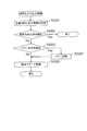
- FIG. 2 is a flowchart showing an example of a first operation procedure of the SPFS apparatus according to Embodiment 1 of the present invention.
- FIG. 3 is a flowchart showing steps in the position adjustment step (step S120) shown in FIG.
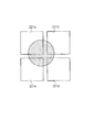
- FIGS. 4A to 4C are schematic diagrams for explaining the step (step S1201) of acquiring the analysis chip position information and the excitation light irradiation unit output information.
- 5A and 5B are graphs showing examples of detection results of reflected light by the first light receiving sensor.
- FIG. 6A and 6B are schematic diagrams for explaining a modification of the step (step S1201) of obtaining the analysis chip position information and the excitation light irradiation unit output information.
- FIG. 7 is a cross-sectional view showing another example of the analysis chip.
- 8A and 8B are schematic diagrams for explaining the process of placing the analysis chip at the measurement position (process S1204).
- FIGS. 9A and 9B are schematic diagrams for explaining the step of placing the analysis chip at the measurement position (step S1204).
- FIG. 10 is a flowchart showing an example of a second operation procedure of the SPFS apparatus according to Embodiment 1 of the present invention.
- FIG. 11A is a flowchart showing steps in the position adjustment step (step S220) shown in FIG. 10, and FIG.
- FIG. 11B is a flowchart showing steps in the calculation and correction step (step S255) shown in FIG. .
- FIG. 12 is a flowchart showing an example of an operation procedure of the SPFS apparatus according to Embodiment 2 of the present invention.
- FIG. 13 is a flowchart showing the steps in the position and output adjustment step (step S320) shown in FIG.
- FIG. 14 is a schematic diagram for explaining a step (step S3201) of acquiring output information of the excitation light irradiation unit when a PD having four light receiving surfaces is used.
- FIG. 15 is a graph for explaining another method for obtaining information on the power of the excitation light irradiation unit.
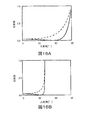
- 16A and 16B are graphs showing the relationship between the incident angle of excitation light and the reflectance.
- a surface plasmon resonance fluorescence analyzer (SPFS apparatus) that can acquire information on the power of an excitation light irradiation unit as output information of the excitation light irradiation unit (excitation light irradiation unit) will be described.
- FIG. 1 is a schematic diagram showing a configuration of an SPFS apparatus 100 according to Embodiment 1 of the present invention.
- the SPFS device 100 includes an excitation light irradiation unit (excitation light irradiation unit) 110, an excitation light detection unit (excitation light detection unit) 120, a fluorescence detection unit (fluorescence detection unit) 130, and a liquid feeding unit. 140, a transport unit 150, and a control processing unit (processing unit) 160.
- the SPFS apparatus 100 is used with the analysis chip 10 mounted on the chip holder 154 of the transport unit 150. Therefore, the analysis chip 10 will be described first, and then each component of the SPFS device 100 will be described.
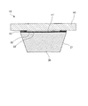
- the analysis chip 10 is arranged on the prism 20 having the incident surface 21, the film formation surface 22 and the emission surface 23, the metal film 30 formed on the film formation surface 22, and the film formation surface 22 or the metal film 30. And a flow path lid 40. Usually, the analysis chip 10 is replaced for each analysis.
- the analysis chip 10 is preferably a structure having a length of several millimeters to several centimeters for each piece, but may be a smaller structure or a larger structure not included in the category of “chip”. Good.
- the prism 20 is made of a dielectric that is transparent to the excitation light ⁇ .
- the prism 20 has an incident surface 21, a film forming surface 22, and an exit surface 23.
- the incident surface 21 causes most of the excitation light ⁇ from the excitation light irradiation unit 110 to enter the prism 20 and reflects a part of the excitation light ⁇ from the excitation light irradiation unit 110.
- the ratio (reflectance) of the amount of excitation light ⁇ hereinafter also referred to as “reflected light ⁇ ” reflected by the incident surface 21 is the refractive index of the prism 20.
- the refractive index of the gas around the prism 20 and the incident angle of the excitation light ⁇ with respect to the incident surface 21 It is determined according to the refractive index of the gas around the prism 20 and the incident angle of the excitation light ⁇ with respect to the incident surface 21 (see the reference experiment described later). Since the surroundings of the prism 20 are usually air, the reflectance is almost constant if the material of the prism 20 and the incident angle of the excitation light ⁇ are the same. For example, when the material of the prism 20 is a resin having a refractive index of 1.4 to 1.6, the reflectance is about 4.2%.
- a metal film 30 is disposed on the film formation surface 22.
- the excitation light ⁇ incident on the inside of the prism 20 is reflected on the back surface of the metal film 30. More specifically, the excitation light ⁇ is reflected at the interface (deposition surface 22) between the prism 20 and the metal film 30.
- the emission surface 23 emits the excitation light ⁇ reflected by the metal film 30 to
- the shape of the prism 20 is not particularly limited.
- the shape of the prism 20 is a column having a trapezoidal bottom surface.
- the surface corresponding to one base of the trapezoid is the film formation surface 22, the surface corresponding to one leg is the incident surface 21, and the surface corresponding to the other leg is the emission surface 23.
- the trapezoid serving as the bottom surface is preferably an isosceles trapezoid. Thereby, the entrance surface 21 and the exit surface 23 are symmetric, and the S wave component of the excitation light ⁇ is less likely to stay in the prism 20.
- the incident surface 21 is formed so that the excitation light ⁇ does not return to the excitation light irradiation unit 110.
- the light source of the excitation light ⁇ is a laser diode (hereinafter also referred to as “LD”)
- LD laser diode
- the angle of the incident surface 21 is set so that the excitation light ⁇ does not enter the incident surface 21 perpendicularly in the scanning range centered on the ideal enhancement angle.
- the “enhancement angle” means scattered light having the same wavelength as the excitation light ⁇ emitted above the analysis chip 10 when the incident angle of the excitation light ⁇ with respect to the metal film 30 is scanned (hereinafter referred to as “plasmon scattered light”). It means the incident angle when the light quantity of ⁇ is maximized.
- the angle between the incident surface 21 and the film formation surface 22 and the angle between the film formation surface 22 and the emission surface 23 are both about 80 °.
- the enhancement angle (and the resonance angle near the pole) is generally determined by the design of the analysis chip 10.
- the design factors are the refractive index of the prism 20, the refractive index of the metal film 30, the film thickness of the metal film 30, the extinction coefficient of the metal film 30, the wavelength of the excitation light ⁇ , and the like.
- the enhancement angle and the resonance angle are shifted by the substance to be detected immobilized on the metal film 30, but the amount is less than a few degrees.
- the “resonance angle” means that when the incident angle of the excitation light ⁇ with respect to the metal film 30 is scanned, the amount of reflected light (not shown) reflected by the film formation surface 22 and emitted from the emission surface 23 is minimized. Means the incident angle.
- the prism 20 has a considerable amount of birefringence.
- the material of the prism 20 include resin and glass.
- the resin constituting the prism 20 include polymethyl methacrylate (PMMA), polycarbonate (PC), and cycloolefin-based polymer.
- the material of the prism 20 is preferably a resin having a refractive index of 1.4 to 1.6 and a small birefringence.
- the metal film 30 is disposed on the film formation surface 22 of the prism 20.
- an interaction (surface plasmon resonance) occurs between the photon of the excitation light ⁇ incident on the film formation surface 22 under the total reflection condition and free electrons in the metal film 30, and is locally on the surface of the metal film 30. In-situ light can be generated.
- the material of the metal film 30 is not particularly limited as long as it is a metal that can cause surface plasmon resonance.
- Examples of the material of the metal film 30 include gold, silver, copper, aluminum, and alloys thereof.
- the metal film 30 is a gold thin film.
- the method for forming the metal film 30 is not particularly limited. Examples of the method for forming the metal film 30 include sputtering, vapor deposition, and plating.
- the thickness of the metal film 30 is not particularly limited, but is preferably in the range of 30 to 70 nm.
- a capturing body for capturing a substance to be detected is immobilized on the surface of the metal film 30 that does not face the prism 20 (the surface of the metal film 30). By immobilizing the capturing body, it becomes possible to selectively detect the substance to be detected.
- the capturing body is uniformly fixed in a predetermined region (reaction field) on the metal film 30.
- the type of capturing body is not particularly limited as long as it can capture the substance to be detected.
- the capturing body is an antibody or a fragment thereof that can specifically bind to the substance to be detected. In the reaction field, reactions such as binding of the capturing body and the substance to be detected (primary reaction) and fluorescent labeling (secondary reaction) of the substance to be detected are performed.
- the flow path lid 40 is disposed on the metal film 30.
- the flow path lid 40 may be disposed on the film formation surface 22.
- a channel groove is formed on the back surface of the channel lid 40, and the channel lid 40 forms a channel 41 through which a liquid flows together with the metal film 30 (and the prism 20).
- the capturing body fixed to the metal film 30 is exposed in the flow path 41. Both ends of the channel 41 are respectively connected to an inlet and an outlet (not shown) formed on the upper surface of the channel lid 40.
- the channel lid 40 is preferably made of a material that is transparent to light (fluorescence ⁇ and plasmon scattered light ⁇ ) emitted from the metal film 30.
- An example of the material of the flow path lid 40 includes a resin. As long as it is transparent to these lights, the other part of the flow path lid 40 may be formed of an opaque material.
- the flow path lid 40 is bonded to the metal film 30 or the prism 20 by, for example, adhesion using a double-sided tape or an adhesive, laser welding, ultrasonic welding, or pressure bonding using a clamp member.
- the type of liquid flowing through the flow path 41 is not particularly limited.
- the types of liquid include a specimen containing a substance to be detected, a fluorescent labeling solution containing a fluorescent substance, and a buffer solution.
- the specimen include body fluids such as blood, serum, plasma, urine, nasal fluid, saliva, semen, and diluted solutions thereof.
- substances to be detected include nucleic acids (such as DNA and RNA), proteins (such as polypeptides and oligopeptides), amino acids, carbohydrates, lipids, and modified molecules thereof.
- the excitation light ⁇ enters the prism 20 from the incident surface 21. At this time, a part of the excitation light ⁇ is reflected by the incident surface 21 to become reflected light ⁇ .
- the excitation light ⁇ incident on the prism 20 is incident on the metal film 30 at a total reflection angle (an angle at which surface plasmon resonance occurs).
- localized field light (generally also referred to as “evanescent light” or “near field light”) is applied to the metal film 30. Can be generated. This localized field light excites a fluorescent substance that labels the substance to be detected present on the metal film 30, and emits fluorescence ⁇ .
- the SPFS device 100 detects the presence or amount of the substance to be detected by detecting the light quantity (intensity) of the fluorescent ⁇ emitted from the fluorescent substance. Although details will be described later, the SPFS device 100 can acquire the position information of the analysis chip 10 and the output information of the excitation light irradiation unit 110 by detecting the light amount (intensity) of the reflected light ⁇ . .
- the SPFS device 100 includes the excitation light irradiation unit (excitation light irradiation unit) 110, the excitation light detection unit (excitation light detection unit) 120, the fluorescence detection unit 130, the liquid feeding unit 140, the transport unit 150, and the control processing unit. (Processing unit) 160.
- the excitation light irradiation unit 110 irradiates the analysis chip 10 held by the chip holder 154 with excitation light ⁇ .
- the excitation light irradiation unit 110 emits only the P wave toward the incident surface 21 so that the incident angle with respect to the metal film 30 is an angle that causes surface plasmon resonance.
- the “excitation light” is light that directly or indirectly excites the fluorescent material.
- the excitation light ⁇ is light that generates localized field light on the surface of the metal film 30 that excites the fluorescent material when the metal film 30 is irradiated through the prism 20 at an angle at which surface plasmon resonance occurs. is there.
- the excitation light ⁇ is also used for positioning the analysis chip 10 and detecting an abnormality of the excitation light irradiation unit 110.
- the excitation light irradiation unit 110 includes a configuration for emitting the excitation light ⁇ toward the prism 20 and a configuration for scanning the incident angle of the excitation light ⁇ with respect to the back surface of the metal film 30.
- the excitation light irradiation unit 110 includes a light source unit 111, an angle adjustment mechanism 112, and a light source control unit 113.
- the light source unit 111 emits the collimated excitation light ⁇ having a constant wavelength and light amount (intensity) so that the shape of the irradiation spot on the back surface of the metal film 30 is substantially circular.
- the light source unit 111 includes, for example, a light source of excitation light ⁇ , a beam shaping optical system, and a temperature adjustment mechanism (all not shown).
- the type of the light source is not particularly limited, but is preferably a high power light source from the viewpoint of using a non-sensitive photodetector such as a photodiode (PD) as the second light receiving sensor 137.
- the light source is a laser diode (LD).
- Other examples of light sources include light emitting diodes, mercury lamps, and other laser light sources.
- the light emitted from the light source is converted into monochromatic light by a diffraction grating or the like. Furthermore, when the light emitted from the light source is not linearly polarized light, the light emitted from the light source is converted into linearly polarized light by a polarizer or the like.
- the beam shaping optical system includes, for example, a collimator, a band pass filter, a linear polarization filter, a half-wave plate, a slit, and a zoom means.
- the beam shaping optical system may include all of these or a part thereof.
- the collimator collimates the excitation light ⁇ emitted from the light source.
- the bandpass filter turns the excitation light ⁇ emitted from the light source into a narrow band light having only the center wavelength. This is because the excitation light ⁇ from the light source has a slight wavelength distribution width.
- the linear polarization filter turns the excitation light ⁇ emitted from the light source into completely linearly polarized light.
- the half-wave plate adjusts the polarization direction of the excitation light ⁇ so that the P-wave component is incident on the metal film 30.
- the slit and zoom means adjust the beam diameter, contour shape, and the like of the excitation light ⁇ so that the shape of the irradiation spot on the back surface of the metal film 30 is a circle having a predetermined size.
- the temperature adjustment mechanism is, for example, a heater or a Peltier element.
- the wavelength and energy of the light emitted from the light source may vary depending on the temperature. For this reason, the wavelength and energy of the light emitted from the light source are controlled to be constant by keeping the temperature of the light source constant by the temperature adjusting mechanism.
- the angle adjustment mechanism 112 adjusts the incident angle of the excitation light ⁇ to the metal film 30 (the interface between the prism 20 and the metal film 30 (film formation surface 22)). In order to irradiate the excitation light ⁇ at a predetermined incident angle toward a predetermined position of the metal film 30 via the prism 20, the angle adjustment mechanism 112 relatively sets the optical axis of the excitation light ⁇ and the chip holder 154 relatively. Rotate.
- the angle adjustment mechanism 112 rotates the light source unit 111 around an axis (axis perpendicular to the paper surface of FIG. 1) orthogonal to the optical axis of the excitation light ⁇ .
- the position of the rotation axis is set so that the position of the irradiation spot on the metal film 30 hardly changes even when the incident angle is scanned.
- the angle at which the maximum amount of plasmon scattered light ⁇ can be obtained is the enhancement angle.
- the basic incident condition of the excitation light ⁇ is determined by the material and shape of the prism 20 of the analysis chip 10, the film thickness of the metal film 30, the refractive index of the liquid in the flow path, and the like.
- the optimum incident condition varies slightly depending on the type and amount of the light and the shape error of the prism 20. For this reason, it is preferable to obtain an optimal enhancement angle for each measurement.
- a suitable emission angle of the excitation light ⁇ with respect to the normal line of the metal film 30 is about 70 °.
- the light source control unit 113 controls various devices included in the light source unit 111 to control the output of the emitted light (excitation light ⁇ ) of the light source unit 111.
- the light source control unit 113 includes, for example, a known computer or microcomputer including an arithmetic device, a control device, a storage device, an input device, and an output device.
- the excitation light detection unit 120 performs positioning of the analysis chip 10 and abnormality detection of the excitation light irradiation unit 110 when performing optical measurement (for example, detection of an enhancement angle, measurement of an optical blank value, detection of fluorescence ⁇ , etc.). Therefore, the reflected light ⁇ generated by irradiating the analysis chip 10 with the excitation light ⁇ is detected.
- the excitation light detection unit 120 detects the reflected light ⁇ for positioning the analysis chip 10 and detecting an abnormality of the excitation light irradiation unit 110 before performing the first optical measurement.
- the first optical measurement is detection of the enhancement angle
- the reflected light ⁇ is detected before measuring the optical blank value.
- the reflected light ⁇ is detected before the detection of the fluorescence ⁇ .
- the detection of the reflected light ⁇ for detecting the abnormality of the excitation light irradiation unit 110 and the detection of the reflected light ⁇ for positioning the analysis chip 10 may be performed simultaneously or separately. . In the present embodiment, detection of the reflected light ⁇ for detecting an abnormality of the excitation light irradiation unit 110 and detection of the reflected light ⁇ for positioning the analysis chip 10 are performed simultaneously.
- the excitation light detection unit 120 includes a first light receiving sensor 121 and a first sensor control unit 122.
- the first light receiving sensor 121 detects the reflected light ⁇ of the excitation light ⁇ .
- the type of the first light receiving sensor 121 is not particularly limited as long as the reflected light ⁇ of the excitation light ⁇ can be detected.
- the first light receiving sensor 121 is a photodiode (PD), a position detection element (PSD), or the like.
- the size of the light receiving surface of the first light receiving sensor 121 is preferably larger than the beam diameter of the excitation light ⁇ . For example, when the beam diameter of the excitation light ⁇ is about 1 to 1.5 mm, the length of one side of the light receiving surface of the first light receiving sensor 121 is preferably 3 mm or more.
- the first light receiving sensor 121 is disposed at a position where the reflected light ⁇ of the excitation light ⁇ is incident. In the present embodiment, the first light receiving sensor 121 is disposed at a position where the reflected light ⁇ from the incident surface 21 is incident. Preferably, the first light receiving sensor 121 is disposed at a position where the reflected light ⁇ of the excitation light ⁇ emitted at the same angle as or close to the detection of the fluorescence ⁇ is incident. Since the irradiation position (irradiation direction) of the excitation light ⁇ slightly changes depending on the change in the incident angle, the incident angle of the excitation light ⁇ is the same or close to that at the time of positioning the analysis chip 10 and the detection of the fluorescence ⁇ .
- the emission angle of the excitation light ⁇ with respect to the normal line of the metal film 30 is about 70 °
- the reflected light ⁇ from the incident surface 21 is reflected on the transport stage. It proceeds almost horizontally in the direction of travel (the x axis direction in FIG. 1). Therefore, the first light receiving sensor 121 is disposed at a position where the reflected light ⁇ traveling in the horizontal direction is incident (see FIG. 4C).
- the first sensor control unit 122 detects the output value of the first light receiving sensor 121, manages the sensitivity of the first light receiving sensor 121 based on the detected output value, and acquires the appropriate output value of the first light receiving sensor 121. Control sensitivity changes.
- the first sensor control unit 122 includes, for example, a known computer or microcomputer including an arithmetic device, a control device, a storage device, an input device, and an output device.
- the fluorescence detection unit 130 detects the fluorescence ⁇ generated by irradiating the metal film 30 with the excitation light ⁇ . Further, as necessary, the fluorescence detection unit 130 also detects plasmon scattered light ⁇ generated by irradiation of the excitation light ⁇ to the metal film 30.
- the fluorescence detection unit 130 includes, for example, a light receiving unit 131, a position switching mechanism 132, and a second sensor control unit 133.
- the light receiving unit 131 is arranged in the normal direction of the metal film 30 of the analysis chip 10 (z-axis direction in FIG. 1).
- the light receiving unit 131 includes a first lens 134, an optical filter 135, a second lens 136, and a second light receiving sensor 137.
- the first lens 134 is, for example, a condensing lens, and condenses light emitted from the metal film 30.
- the second lens 136 is, for example, an imaging lens, and forms an image of the light collected by the first lens 134 on the light receiving surface of the second light receiving sensor 137.
- the optical path between both lenses is a substantially parallel optical path.
- the optical filter 135 is disposed between the first lens 134 and the second lens 136. At the time of fluorescence detection, the optical filter 135 transmits only the fluorescence component of the light incident on the optical filter 135 and removes the excitation light component (plasmon scattered light ⁇ ). Thereby, only the fluorescence component is guided to the second light receiving sensor 137, and the fluorescence ⁇ can be detected with a high S / N ratio.
- types of the optical filter 135 include an excitation light reflection filter, a short wavelength cut filter, and a band pass filter.
- Examples of the optical filter 135 include a filter including a multilayer film that reflects a predetermined light component, and a color glass filter that absorbs the predetermined light component.
- the second light receiving sensor 137 detects fluorescence ⁇ and plasmon scattered light ⁇ emitted from the analysis chip 10.
- Examples of the second light receiving sensor 137 include a photodiode (PD), a photomultiplier tube (PMT), and an avalanche photodiode (APD).
- PD photodiode
- PMT photomultiplier tube
- APD avalanche photodiode
- the position switching mechanism 132 switches the position of the optical filter 135 on or off the optical path in the light receiving unit 131. Specifically, when the second light receiving sensor 137 detects fluorescence ⁇ , the optical filter 135 is disposed on the optical path of the light receiving unit 131, and when the second light receiving sensor 137 detects plasmon scattered light ⁇ , the optical filter 135 is disposed. Is arranged outside the optical path of the light receiving unit 131.
- the position switching mechanism 132 includes, for example, a rotation drive unit and a known mechanism (such as a turntable or a rack and pinion) that moves the optical filter 135 in the horizontal direction using a rotational motion.
- the second sensor control unit 133 detects the output value of the second light receiving sensor 137, manages the sensitivity of the second light receiving sensor 137 based on the detected output value, and acquires the appropriate output value of the second light receiving sensor 137. Control sensitivity changes.
- the second sensor control unit 133 is configured by, for example, a known computer or microcomputer including an arithmetic device, a control device, a storage device, an input device, and an output device.
- the liquid feeding unit 140 supplies a sample liquid, a labeling liquid, a cleaning liquid, and the like into the flow path 41 of the analysis chip 10 held by the chip holder 154.
- the liquid feeding unit 140 includes a chemical liquid chip 141, a syringe pump 142, and a liquid feeding pump drive mechanism 143.
- the chemical solution chip 141 is a container for storing a liquid such as a sample solution, a labeling solution, or a cleaning solution.
- a liquid such as a sample solution, a labeling solution, or a cleaning solution.
- a plurality of containers are usually arranged according to the type of liquid, or a chip in which a plurality of containers are integrated is arranged.
- the syringe pump 142 includes a syringe 144 and a plunger 145 that can reciprocate inside the syringe 144.
- the plunger 145 By the reciprocating motion of the plunger 145, the liquid is sucked and discharged quantitatively. If the syringe 144 can be replaced, the syringe 144 need not be cleaned. For this reason, it is preferable from the viewpoint of preventing contamination of impurities.
- the syringe 144 is not configured to be replaceable, it is possible to use the syringe 144 without replacing it by adding a configuration for cleaning the inside of the syringe 144.
- the liquid feed pump driving mechanism 143 includes a driving device for the plunger 145 and a moving device for the syringe pump 142.
- the drive device of the syringe pump 142 is a device for reciprocating the plunger 145, and includes, for example, a stepping motor.
- the drive device including the stepping motor is preferable from the viewpoint of managing the remaining liquid amount of the analysis chip 10 because it can manage the liquid feeding amount and the liquid feeding speed of the syringe pump 142.
- the moving device of the syringe pump 142 moves the syringe pump 142 freely in two directions, for example, an axial direction (for example, a vertical direction) of the syringe 144 and a direction crossing the axial direction (for example, a horizontal direction).
- the moving device of the syringe pump 142 is configured by, for example, a robot arm, a two-axis stage, or a turntable that can move up and down.
- the liquid feeding unit 140 determines the position of the tip of the syringe 144. It is preferable to further have a device for detecting.
- the liquid feeding unit 140 sucks various liquids from the chemical liquid chip 141 and supplies them to the flow path 41 of the analysis chip 10. At this time, by moving the plunger 145, the liquid reciprocates in the flow path 41 in the analysis chip 10, and the liquid in the flow path 41 is stirred. As a result, it is possible to achieve a uniform concentration of the liquid and promotion of a reaction (for example, an antigen-antibody reaction) in the channel 41. From the viewpoint of performing such an operation, the analysis chip 10 and the syringe 144 are protected by a multilayer film, and the analysis chip 10 and the syringe 144 can be sealed when the syringe 144 penetrates the multilayer film. It is preferable to be configured.
- the liquid in the channel 41 is again sucked by the syringe pump 142 and discharged to the chemical liquid chip 141 and the like.
- reaction with various liquids, washing, and the like can be performed, and a target substance labeled with a fluorescent substance can be placed in the reaction field in the flow path 41.
- the transport unit 150 transports and fixes the analysis chip 10 to the installation position, the measurement position, or the liquid feeding position.
- the “installation position” is a position for installing the analysis chip 10 in the SPFS apparatus 100 (more specifically, the chip holder 154).
- the “measurement position” is a position where the fluorescence detection unit 130 detects the fluorescence ⁇ that is generated when the excitation light irradiation unit 110 irradiates the analysis chip 10 with the excitation light ⁇ .
- the “liquid feeding position” is a position where the liquid feeding unit 140 supplies a liquid into the flow channel 41 of the analysis chip 10 or removes the liquid in the flow channel 41 of the analysis chip 10.
- the transfer unit 150 includes a transfer stage 152 and a chip holder 154.
- the transfer stage 152 moves the chip holder 154 in one direction (x-axis direction in FIG. 1) and in the opposite direction.
- the transfer stage 152 is driven by, for example, a stepping motor.
- the chip holder 154 is fixed to the transfer stage 152 and holds the analysis chip 10 in a detachable manner.
- the shape of the chip holder 154 is a shape that can hold the analysis chip 10 and does not obstruct the optical path of light such as excitation light ⁇ , reflected light ⁇ , and fluorescence ⁇ .
- the chip holder 154 is provided with an opening through which these lights pass.
- the control processing unit 160 controls the angle adjustment mechanism 112, the light source control unit 113, the first sensor control unit 122, the position switching mechanism 132, the second sensor control unit 133, the liquid feed pump drive mechanism 143, and the transport stage 152.
- the control processing unit 160 acquires the position information of the analysis chip 10 and the output information of the excitation light irradiation unit 110 based on the detection result of the excitation light detection unit 120.
- the control processing unit 160 specifies the position of the analysis chip 10 held by the chip holder 154 based on the acquired position information.
- the control processing unit 160 stores output information that is acquired in advance and serves as a reference for the excitation light irradiation unit 110.
- the control processing unit 160 determines whether or not the excitation light irradiation unit 110 is normal by comparing the acquired output information with reference output information.
- the output information of the excitation light irradiation unit 110 is information regarding the power of the excitation light irradiation unit 110, information regarding the irradiation direction of the excitation light ⁇ , or both.
- the reference output information is output information of the excitation light irradiation unit 110 in a normal state, for example, the excitation light irradiation unit 110 in the initial state.
- the output information of the excitation light irradiation unit 110 is information regarding the power of the excitation light irradiation unit 110.
- standard is the output information of the excitation light irradiation unit 110 in an initial state.
- the control processing unit 160 includes, for example, a known computer or microcomputer including an arithmetic device, a control device, a storage device, an input device, and an output device.
- the SPFS device 100 can perform, for example, two operations described later.
- the SPFS device 100 acquires information regarding the power of the excitation light irradiation unit 110 as output information of the excitation light irradiation unit 110.
- the SPFS device 100 adjusts the power of the excitation light irradiation unit 110.
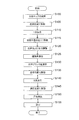
- FIG. 2 is a flowchart showing an example of a first operation procedure of the SPFS device 100.
- FIG. 3 is a flowchart showing steps in the position and output adjustment step (step S120) shown in FIG. In the first operation, an abnormality detection step (step S1202) is included in the position and output adjustment step (step S120).
- the analysis chip 10 is installed at the installation position of the SPFS device 100 (step S100). Specifically, the analysis chip 10 is installed in the chip holder 154 of the SPFS device 100.
- control processing unit 160 operates the transfer stage 152 to move the analysis chip 10 to the liquid feeding position (step S105).
- control processing unit 160 operates the liquid feeding unit 140 to introduce the sample liquid in the chemical liquid chip 141 into the flow path 41 of the analysis chip 10 (step S110).
- the substance to be detected is captured on the metal film 30 by the antigen-antibody reaction (primary reaction).
- the sample liquid in the flow path 41 is removed, and the flow path 41 is cleaned with a cleaning liquid.
- the humectant is washed by washing the flow channel 41 before introducing the sample solution so that the capturing body can appropriately capture the substance to be detected. Remove.
- control processing unit 160 operates the transfer stage 152 to move the analysis chip 10 to the vicinity of the measurement position (step S115).
- control processing unit 160 operates the excitation light irradiation unit 110, the excitation light detection unit 120, and the transport stage 152, and acquires the position information of the analysis chip 10 and the output information of the excitation light irradiation unit 110.
- the control processing unit 160 adjusts the position of the analysis chip 10 based on the acquired position information. Further, the control processing unit 160 determines whether or not the excitation light irradiation unit 110 is normal based on the acquired output information. If the control processing unit 160 determines that the power of the excitation light irradiation unit 110 is abnormal, the control processing unit 160 adjusts the power of the excitation light irradiation unit 110 based on the acquired output information (step S120).
- the analysis chip 10 held by the chip holder 154 is irradiated with the excitation light ⁇ and reflected by the excitation light ⁇ reflected by the surface of the analysis chip 10. Is detected, and position information of the analysis chip 10 and output information (information about power) of the excitation light irradiation unit 110 are acquired (step S1201).
- control processing unit 160 determines whether or not the power of the excitation light irradiation unit 110 (more specifically, the light source unit 111) is normal based on the output information (step S1202).
- the control processing unit 160 stores information about the power of the excitation light irradiation unit 110 in the initial state. More specifically, in the control processing unit 160, the intensity of the reflected light ⁇ from the surface of the analysis chip 10 of the excitation light ⁇ emitted from the excitation light irradiation unit 110 in the initial state (hereinafter simply referred to as “initial value”). Is stored).
- the control processing unit 160 compares the detection value of the reflected light ⁇ detected in step S121 with the initial value stored in the control processing unit 160 in advance, so that the power of the excitation light irradiation unit 110 is normal. Determine whether. For example, when the difference between the initial value and the detected value exceeds a predetermined reference value (threshold value), the control processing unit 160 determines that the power of the excitation light irradiation unit 110 is abnormal.
- This reference value (threshold value) can be appropriately set according to the accuracy required for the analysis.
- control processing unit 160 determines that the power of the excitation light irradiation unit 110 is decreasing (abnormal)
- the control processing unit 160 adjusts the output of the excitation light irradiation unit 110 to an intended power (step S1203).
- the control processing unit 160 continues the subsequent operation.
- control processing unit 160 adjusts the position of the analysis chip 10 based on the position information of the analysis chip 10 (step S1204). Although details will be described later, the control processing unit 160 can specify the degree of positional deviation of the analysis chip 10 from the measurement position based on the position information. Based on the acquired position information, the control processing unit 160 operates the transfer stage 152 and moves the chip holder 154 to place the analysis chip 10 at an appropriate measurement position.
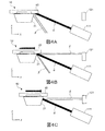
- FIG. 4A and 4B are schematic diagrams for explaining the step (S1201) of acquiring the position information of the analysis chip 10 and the output information of the excitation light irradiation unit 110.
- FIG. 4A when the analysis chip 10 is located away from the light source unit 111, when the light source unit 111 emits the excitation light ⁇ , the excitation light ⁇ is reflected by the channel lid 40 and To the side (conveyance stage 152 side). Therefore, the reflected light ⁇ from the surface of the analysis chip 10 does not enter the first light receiving sensor 121 of the excitation light detection unit 120.
- the excitation light ⁇ from the light source unit 111 reaches the boundary portion (hereinafter referred to as “edge portion”) between the prism 20 and the channel lid 40.
- edge portion the boundary portion between the prism 20 and the channel lid 40.
- the excitation light ⁇ (reflected light ⁇ ) reflected by the flow path lid 40 does not enter the first light receiving sensor 121, but the excitation light ⁇ (reflected light ⁇ ) reflected by the incident surface 21. ) Enters the first light receiving sensor 121. Therefore, a part of the reflected light ⁇ from the analysis chip 10 enters the first light receiving sensor 121.
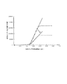
- FIG. 5A and 5B are graphs showing examples of detection results of the reflected light ⁇ by the first light receiving sensor 121.
- the beam diameter of the excitation light ⁇ is about 1 to 1.5 mm.
- FIG. 5A shows only the detection results, and FIG. 5B also shows three approximate lines.
- the reflected light ⁇ from the surface of the analysis chip 10 does not enter the first light receiving sensor 121 when the movement distance of the analysis chip 10 is 0 to about 1000 ⁇ m. This is because the excitation light ⁇ is reflected by the flow path lid 40 and travels downward (on the conveyance stage 152 side) (see FIG. 4A).
- the intensity of the reflected light ⁇ incident on the first light receiving sensor 121 gradually increases. This is because a part of the excitation light ⁇ is reflected by the incident surface 21 and enters the first light receiving sensor 121 (see FIG. 4B).
- the intensity of the reflected light ⁇ incident on the first light receiving sensor 121 becomes substantially constant and maximum. This is because all of the reflected light ⁇ is incident on the first light receiving sensor 121 (see FIG. 4C). Therefore, the inclined portion (movement distance: about 1000 to about 2000 ⁇ m) in the graph corresponds to the edge portion.
- the width of the inclined portion corresponds to the beam diameter (about 1 to 1.5 mm) of the excitation light ⁇ in the x-axis direction.
- the first horizontal portion (movement distance: 0 to about 1000 ⁇ m), the slope portion (movement distance: about 1000 to about 2000 ⁇ m), and the second half horizontal portion (movement distance: more than about 2000 ⁇ m) are linearly approximated.
- Point A in the graph is an intersection of the approximate straight line of the horizontal portion and the approximate straight line of the inclined portion in the first half.
- Point B is an intersection of the approximate straight line of the inclined portion and the approximate straight line of the second horizontal portion.
- Point C is the midpoint between points A and B.
- Point A corresponds to the minimum value of the intensity of the reflected light ⁇ .
- Point B corresponds to the maximum value of the intensity of the reflected light ⁇ .
- Point C corresponds to an intermediate value of the intensity of the reflected light ⁇ .
- any one of the points A to C may be used.
- Point A and point B indicate points where the edge of the beam of excitation light ⁇ has reached the edge. Therefore, if the beam diameter of the excitation light ⁇ is taken into consideration, the position of the edge portion can be specified, and as a result, the position of the analysis chip 10 can be specified.
- a point C indicates a point where the center of the beam of the excitation light ⁇ has reached the edge part. When the point C is used, the position of the edge portion can be specified without considering the beam diameter of the excitation light ⁇ , and as a result, the position of the analysis chip 10 can be specified. Therefore, from the viewpoint of suppressing the influence of the beam diameter of the excitation light ⁇ , it is preferable to specify the position of the analysis chip 10 using an intermediate value of the intensity of the reflected light ⁇ of the excitation light ⁇ .
- Point B is the maximum value of the intensity of the reflected light ⁇ of the excitation light ⁇ emitted from the excitation light irradiation unit 110, and is also the output value of the excitation light ⁇ emitted from the irradiation light irradiation unit 110. Therefore, by comparing the maximum value of the intensity of the reflected light ⁇ with the initial value, it is possible to determine whether or not the power of the excitation light irradiation unit 110 (light source unit 111) is reduced.
- the position of the analysis chip 10 is specified by irradiating the analysis chip 10 with the excitation light ⁇ and detecting the reflected light ⁇ of the excitation light ⁇ reflected on the surface of the analysis chip 10. Can do.
- the analysis chip 10 It is preferable to specify the position of the analysis chip 10 by irradiating two surfaces adjacent to each other with excitation light ⁇ .
- the transport stage 152 it is preferable to irradiate the excitation light ⁇ in a direction that is not parallel or perpendicular to the moving direction of the chip holder 154 by the transport stage 152.
- FIG. 6A even if the first light receiving sensor 121 is arranged at a position where the reflected light ⁇ from the flow path lid 40 is incident and the reflected light ⁇ from the incident surface 21 is not incident, FIG.
- the same effect as the example shown in C can be obtained (the intensity of the reflected light ⁇ increases when the moving distance is short and decreases when the moving distance is long).
- the position of the incident surface 21 is particularly important, when the excitation light ⁇ is irradiated onto two surfaces adjacent to each other of the analysis chip 10, the surfaces adjacent to the incident surface 21 and the incident surface 21 of the analysis chip 10. (In this embodiment, it is preferable to irradiate the back surface of the channel lid 40 with the excitation light ⁇ . In this case, as shown in FIG. 6B, the excitation light ⁇ may be applied to the incident surface 21 of the prism 20 and the lower surface of the prism 20. However, in the example shown in FIG. 6B, when the position of the analysis chip 10 is specified (step S1201), the analysis chip 10 comes closer to the light source unit 111 than the measurement position.
- the chip holder 154 when the analysis chip 10 is moved to the measurement position (step S1204), the chip holder 154 must be moved in the reverse direction by the transfer stage 152. In this way, operating the transfer stage 152 in two directions may lead to a decrease in operation accuracy as compared with the case where the transfer stage 152 is operated only in one direction. On the other hand, in the example shown in FIGS. 4A to 4C and FIG. 6A, it is not necessary to move the chip holder 154 in the reverse direction by the transfer stage 152.
- the transfer stage 152 it is preferable to move the chip holder 154 only in the direction approaching the light source (light source unit 111) of the excitation light ⁇ (x-axis direction).
- the “two adjacent surfaces of the analysis chip 10” includes two substantially adjacent surfaces.
- the prism 20, the metal film 30 disposed on the prism film-forming surface 22, the spacer 42 disposed on the metal film 30, and the spacer 42 are disposed.
- an analysis chip 10 ′ having a channel cover 40 is used.
- the shape of the flow path 41 is formed by the spacer 42.
- the channel lid 40 is a transparent flat plate. In this case, strictly speaking, since the side surface of the spacer 42 exists between the incident surface 21 of the prism 20 and the lower surface of the flow path lid 40, the incident surface 21 and the lower surface of the flow path lid 40 are not adjacent to each other.
- the spacer 42 is very thin (for example, 100 ⁇ m) compared to the beam diameter (for example, 1 to 1.5 mm) of the excitation light ⁇ , the incident surface 21 and the lower surface of the channel lid 40 are substantially adjacent to each other. It is thought that. Therefore, in this case, the reflected light ⁇ from the substantially adjacent incident surface 21 and the lower surface of the flow path lid 40 is detected to detect the edge portion. Similarly, a bonding member such as an adhesive or a double-sided tape or the metal film 30 can be ignored.
- the thickness of the member (for example, the spacer 42) that can be ignored when detecting the reflected light ⁇ is 1/5 or less of the beam diameter of the excitation light ⁇ , and preferably 1/10 or less.
- the reflected light ⁇ from the surface of the analysis chip 10 ′ is The majority (4/5 or more or 9/10 or more) is the reflected light ⁇ from the incident surface 21 or the lower surface of the flow path lid 40 and can be used for position detection. Therefore, the position of the analysis chip 10 ′ can be specified without being affected by the spacer 42.
- members having a thickness of 1/5 or less of the beam diameter of the excitation light ⁇ can be ignored when detecting the reflected light ⁇ . That is, the incident surface 21 of the analysis chip 10 ′ and the lower surface of the flow path lid 40 can be considered as two surfaces that are substantially adjacent.
- FIG. 8A and 8B are schematic diagrams for explaining the process of placing the analysis chip 10 at an appropriate measurement position (process S1204).
- process S1204 First, as shown in FIG. 8A, it is assumed that the position of the edge portion is specified. In this case, the distance between the position of the edge portion and the region to be irradiated with the excitation light ⁇ on the back surface of the metal film 30 (region on the back side of the reaction field) is determined. Therefore, as shown in FIG. 8B, the analysis chip 10 can be placed at an appropriate measurement position by moving the chip holder 154 to the transport stage 152 by a predetermined distance.
- the analysis chip 10 when the analysis chip 10 is arranged so as to be shifted in the height direction (z-axis direction) (for example, dust is sandwiched between the analysis chip 10 and the chip holder 154).
- the analysis chip 10 can be arranged at an appropriate measurement position. That is, as shown in FIG. 9A, it is assumed that the position of the edge portion is specified. In this case, the position of the analysis chip 10 in the x-axis direction is shifted as compared to the case where the analysis chip 10 is not shifted in the z-axis direction (indicated by a broken line in the figure). However, even in this case, as shown in FIG. 9B, the analysis chip 10 is moved to an appropriate measurement position by moving the chip holder 154 to the transport stage 152 by a predetermined distance based on the position of the edge portion. Can be arranged.
- the control processing unit 160 operates the excitation light irradiation unit 110 and the fluorescence detection unit 130 to irradiate the analysis chip 10 disposed at an appropriate measurement position with the excitation light ⁇ and has the same wavelength as the excitation light ⁇ .
- the plasmon scattered light ⁇ is detected to detect the enhancement angle (step S125).
- the control processing unit 160 operates the excitation light irradiation unit 110 to scan the incident angle of the excitation light ⁇ with respect to the metal film 30 and operates the fluorescence detection unit 130 to detect the plasmon scattered light ⁇ . .
- control processing unit 160 operates the position switching mechanism 132 to place the optical filter 135 outside the light path of the light receiving unit 131. Then, the control processing unit 160 determines the incident angle of the excitation light ⁇ when the light amount of the plasmon scattered light ⁇ is the maximum as the enhancement angle.
- control processing unit 160 operates the excitation light irradiation unit 110 and the fluorescence detection unit 130 to irradiate the analysis chip 10 disposed at an appropriate measurement position with the excitation light ⁇ and output the second light receiving sensor 137.
- the value (optical blank value) is recorded (step S130).
- the control processing unit 160 operates the angle adjustment mechanism 112 to set the incident angle of the excitation light ⁇ to the enhancement angle.
- control processing unit 160 controls the position switching mechanism 132 to arrange the optical filter 135 in the optical path of the light receiving unit 131.
- control processing unit 160 operates the transfer stage 152 to move the analysis chip 10 to the liquid feeding position (step S135).
- control processing unit 160 operates the liquid feeding unit 140 to introduce a liquid (labeled liquid) containing a secondary antibody labeled with a fluorescent substance into the flow channel 41 of the analysis chip 10 (step S140).
- a liquid labeled liquid
- the detection target substance captured on the metal film 30 is labeled with a fluorescent substance by an antigen-antibody reaction (secondary reaction).
- secondary reaction antigen-antibody reaction
- control processing unit 160 operates the transfer stage 152 to move the analysis chip 10 to the appropriate measurement position determined in step S120 (step S145).
- control processing unit 160 operates the excitation light irradiation unit 110 and the fluorescence detection unit 130 to irradiate the analysis chip 10 disposed at an appropriate measurement position with the excitation light ⁇ and is captured by the capturing body.
- the fluorescence ⁇ emitted from the fluorescent substance that labels the substance to be detected is detected (step S150).
- control processing unit 160 subtracts the optical blank value from the detected value of fluorescence ⁇ , and calculates the fluorescence intensity that correlates with the amount of the substance to be detected (step S155).
- the calculated fluorescence intensity is converted into the amount and concentration of the substance to be detected as necessary.
- the SPFS device 100 acquires information regarding the power of the excitation light irradiation unit 110 as output information of the excitation light irradiation unit 110.
- the SPFS device 100 corrects the detection value of the fluorescence ⁇ according to the power value of the excitation light irradiation unit 110. To do.
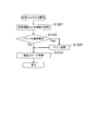
- FIG. 10 is a flowchart showing an example of the second operation procedure of the SPFS device 100.
- FIG. 11A is a flowchart showing the steps in the position adjustment step (S220) shown in FIG. 10, and FIG. 11B shows the steps in the calculation step of fluorescence intensity (S255) correlated with the amount of the substance to be detected shown in FIG. It is a flowchart which shows this process.
- an abnormality detection step step S2552 is included in the calculation step (step S255) of the amount of the substance to be detected.
- the analysis chip 10 is installed at the installation position of the SPFS device 100 (step S200). Specifically, the analysis chip 10 is installed in the chip holder 154 of the SPFS device 100.
- control processing unit 160 operates the transfer stage 152 to move the analysis chip 10 to the liquid feeding position (step S205).
- control processing unit 160 operates the liquid feeding unit 140 to introduce the sample liquid in the chemical liquid chip 141 into the flow path 41 of the analysis chip 10 (step S210).
- the substance to be detected is captured on the metal film 30 by the antigen-antibody reaction (primary reaction).
- the sample liquid in the flow path 41 is removed, and the flow path 41 is cleaned with a cleaning liquid.
- the humectant is washed by washing the flow channel 41 before introducing the sample solution so that the capturing body can appropriately capture the substance to be detected. Remove.
- control processing unit 160 operates the transfer stage 152 to move the analysis chip 10 to the vicinity of the measurement position (step S215).
- control processing unit 160 operates the excitation light irradiation unit 110, the excitation light detection unit 120, and the transport stage 152, and acquires the position information of the analysis chip 10 and the output information of the excitation light irradiation unit 110.
- the control processing unit 160 adjusts the position of the analysis chip 10 based on the acquired position information (step S220).
- the analysis chip 10 held by the chip holder 154 is irradiated with the excitation light ⁇ and reflected by the excitation light ⁇ reflected by the surface of the analysis chip 10.
- Is detected, and position information of the analysis chip 10 and output information (information about power) of the excitation light irradiation unit 110 are acquired (step S2201).
- the output information acquired at this time is recorded in the control processing unit 160.
- the control processing unit 160 adjusts the position of the analysis chip 10 based on the position information of the analysis chip 10 (step S2202).
- the step (step S2201) of acquiring the position information of the analysis chip 10 and the output information of the excitation light irradiation unit 110 is the same as step S1201, and the analysis chip 10 is appropriately measured based on the acquired position information. Since the process (process S2202) to arrange in is the same as process S1204, those explanations are omitted.
- control processing unit 160 detects the enhancement angle in the same manner as in step S125 (step S225).
- control processing unit 160 measures and records the optical blank value in the same manner as in step S130 (step S230).
- control processing unit 160 operates the transfer stage 152 to move the analysis chip 10 to the liquid feeding position (step S235).
- control processing unit 160 labels the detection target substance captured on the metal film 30 with a fluorescent substance in the same manner as in step S140 (step S240).
- control processing unit 160 operates the transfer stage 152 to move the analysis chip 10 to the appropriate measurement position determined in step S220 (step S245).
- control processing unit 160 detects the fluorescence ⁇ emitted from the fluorescent substance that labels the detection target substance captured by the capturing body in the same manner as in step S150 (step S250).
- control processing unit 160 calculates the amount and concentration of the substance to be detected (step S255).
- the optical blank value is subtracted from the detected value of fluorescence ⁇ , and the fluorescence intensity correlated with the amount of the substance to be detected is calculated (step S2551).
- control processing unit 160 determines whether or not the power of the excitation light irradiation unit 110 is normal based on the output information acquired in step S2201 (step S2552).
- the control processing unit 160 stores the detection value of the reflected light ⁇ detected in step S2201 and the initial value of the reflected light ⁇ .
- the control processing unit 160 determines whether or not the power of the excitation light irradiation unit 110 is normal by comparing the detection value with the initial value.
- the control processing unit 160 determines that the power of the excitation light irradiation unit 110 is reduced (abnormal)
- the control processing unit 160 corrects the fluorescence intensity calculated in step S2551 (step S2553). Specifically, the control processing unit 160 calculates how much the power of the excitation light irradiation unit 110 is reduced based on the detected value and the initial value of the reflected light ⁇ , and compensates for the power reduction. Is applied to the fluorescence intensity calculated in step S2551 (for example, when the power of the excitation light irradiation unit 110 is reduced to 70%, 100/70). In this way, the control processing unit 160 corrects the calculated fluorescence intensity. The corrected fluorescence intensity is converted into the amount and concentration of the substance to be detected as necessary.
- the output of the excitation light irradiation unit 110 is detected by detecting the reflected light ⁇ of the excitation light ⁇ .
- Information (information on power) can be acquired.
- the reflected light ⁇ reflected by the surface of the analysis chip 10 is about several percent of the excitation light ⁇ from the excitation light irradiation unit 110, so the first light receiving sensor 121 is saturated. There is nothing.
- the analysis method and the SPFS apparatus 100 it is possible to accurately determine whether or not the excitation light irradiation unit 110 is normal without separately providing a light amount adjustment unit. False detection can be prevented. In addition, labor and cost required for maintenance such as replacement and cleaning of the light amount adjusting parts can be reduced.
- the analysis chip 10 is replaced every time the analysis is performed, and the excitation light ⁇ from the excitation light irradiation unit 110 is always reflected on a clean surface, so that there is no influence due to deterioration of the reflection surface over time or dust. From this point of view, it can be accurately determined whether or not the excitation light irradiation unit 110 is normal.
- the SPFS device 200 according to the second embodiment is different from the SPFS device 100 according to the first embodiment only in the configuration of the first light receiving sensor 221 of the excitation light detection unit 220. Therefore, only the first light receiving sensor 221 will be described as the configuration of the SPFS device 200, and the same components as those of the SPFS device 100 according to the first embodiment are denoted by the same reference numerals, Description is omitted. Moreover, since the analysis chip 10 used in the SPFS apparatus 200 according to the second embodiment is the same as that used in the SPFS apparatus 100 according to the first embodiment, the description thereof is omitted.
- FIG. 1 is a schematic diagram showing a configuration of a surface plasmon resonance fluorescence analyzer (SPFS apparatus) 100 according to Embodiment 2 of the present invention.
- the SPFS apparatus 100 includes an excitation light irradiation unit (excitation light irradiation unit) 110, an excitation light detection unit (excitation light detection unit) 220, a fluorescence detection unit (fluorescence detection unit) 130, and a liquid feeding unit. 140, a transport unit 150, and a control processing unit (processing unit) 160.
- the excitation light detection unit 220 includes a first light receiving sensor 221 and a first sensor control unit 122.
- the first light receiving sensor 221 detects the light amount and position of the reflected light ⁇ .
- the light receiving sensor 221 is a photodiode (PD) or a position detecting element (PSD) having a plurality of light receiving surfaces.
- the number of light receiving surfaces of the first light receiving sensor 221 is not particularly limited, but is preferably four or more.
- the first light receiving sensor 221 is a PD having four light receiving surfaces.
- the size of the light receiving surface of the first light receiving sensor 221 is configured to be larger than the beam diameter of the excitation light ⁇ from the viewpoint of accurately detecting the irradiation position of the excitation light ⁇ . ing.
- the beam diameter of the excitation light ⁇ is about 1 to 1.5 mm
- the length of one side of the light receiving surface of the first light receiving sensor 221 is preferably 3 mm or more.
- the first light receiving sensor 221 is disposed at a position where the reflected light ⁇ of the excitation light ⁇ is incident. In the present embodiment, the first light receiving sensor 221 is disposed at a position where the reflected light ⁇ from the incident surface 21 is incident. Preferably, the first light receiving sensor 221 is disposed at a position where the reflected light ⁇ of the excitation light ⁇ emitted at the same angle as or close to the detection of the fluorescence ⁇ is incident. Since the irradiation position (irradiation position) of the excitation light ⁇ slightly changes due to the change of the incident angle, the incident angle of the excitation light ⁇ is the same or close to that at the time of positioning the analysis chip 10 and the detection of the fluorescence ⁇ .
- the emission angle of the excitation light ⁇ with respect to the normal line of the metal film 30 is about 70 °
- the reflected light ⁇ from the incident surface 21 is reflected on the transport stage. It proceeds almost horizontally in the direction of travel (the x axis direction in FIG. 1). Accordingly, the first light receiving sensor 221 is disposed at a position where the reflected light ⁇ traveling in the horizontal direction is incident.
- the SPFS device 200 acquires, as output information of the excitation light irradiation unit 110, information regarding the power of the excitation light irradiation unit 110 and the irradiation direction of the excitation light ⁇ .
- the SPFS device 200 adjusts the power of the excitation light irradiation unit 110.
- the subsequent operation is stopped.
- FIG. 12 is a flowchart showing an example of the operation procedure of the SPFS device 200.
- FIG. 13 is a flowchart showing the steps in the position and output adjustment step (step S320) shown in FIG.
- an abnormality detection process (process S3202 and process S3203) is included in the position / output adjustment process (process S320).
- the analysis chip 10 is installed at the installation position of the SPFS device 200 (step S300). Specifically, the analysis chip 10 is installed in the chip holder 154 of the SPFS device 200.
- control processing unit 160 operates the transfer stage 152 to move the analysis chip 10 to the liquid feeding position (step S305).
- control processing unit 160 operates the liquid feeding unit 140 to introduce the sample liquid in the chemical liquid chip 141 into the flow path 41 of the analysis chip 10 (step S310).
- the substance to be detected is captured on the metal film 30 by the antigen-antibody reaction (primary reaction).
- the sample liquid in the flow path 41 is removed, and the flow path 41 is cleaned with a cleaning liquid.
- the humectant is washed by washing the flow channel 41 before introducing the sample solution so that the capturing body can appropriately capture the substance to be detected. Remove.
- control processing unit 160 operates the transfer stage 152 to move the analysis chip 10 to the vicinity of the measurement position (step S315).
- control processing unit 160 operates the excitation light irradiation unit 110, the excitation light detection unit 220, and the transfer stage 152 to acquire the position information of the analysis chip 10 and the output information of the excitation light irradiation unit 110.
- the control processing unit 160 adjusts the position of the analysis chip 10 based on the acquired position information, and adjusts the output of the excitation light irradiation unit 110 based on the acquired output information (Step S320).
- the control processing unit 160 determines that the irradiation direction of the excitation light ⁇ of the excitation light irradiation unit 110 is abnormal based on the acquired output information, the subsequent process is stopped.
- the control processing unit 160 determines whether or not the irradiation direction of the excitation light ⁇ from the excitation light irradiation unit 110 is normal based on the acquired output information (step S3202).
- the control processing unit 160 stores information regarding the irradiation direction of the excitation light ⁇ in the initial state of the excitation light irradiation unit 110. More specifically, the control processing unit 160 stores information regarding the irradiation position (hereinafter also simply referred to as “initial position”) of the reflected light ⁇ with respect to the first light receiving sensor 221.
- control processing unit 160 determines the position of the irradiation spot on the first light receiving sensor 221 of the reflected light ⁇ detected in step S3201 and the initial position stored in the control processing unit 160 in advance. By comparing, it is determined whether or not the irradiation direction of the excitation light ⁇ from the excitation light irradiation unit 110 is normal.
- control processing unit 160 When it is determined that the irradiation direction of the excitation light ⁇ is normal, the control processing unit 160 continues the subsequent operation, and determines that the irradiation direction of the excitation light ⁇ is deviated from the intended direction (abnormal). If so, the operation is terminated.
- step S3203 The step of detecting power abnormality (step S3203), the step of adjusting the power of the excitation light irradiation unit 110 (step S3204), and the analysis chip 10 is arranged at an appropriate measurement position based on the positional information of the analysis chip 10. Since the step (step S3205) is the same as steps S1202 to S1204 in Embodiment 1, the description thereof is omitted.
- FIG. 14 illustrates a step (step S3201) of acquiring output information (information regarding the power and the irradiation direction of the excitation light ⁇ ) of the excitation light irradiation unit 110 when a PD having four light receiving surfaces is used.
- the satin portion indicates the irradiation spot of the excitation light ⁇ irradiated on the light receiving surfaces 221a to 221d of the first light receiving sensor 221.
- the first light receiving sensor 221 is a PD having four light receiving surfaces 221a to 221d.
- the excitation light ⁇ is incident on the light receiving surfaces 221a to 221d
- photocurrents Ia to d corresponding to the amount of the reflected light ⁇ irradiated are generated on the light receiving surfaces 221a to 221d, respectively.
- the irradiation position of the excitation light ⁇ in the in-plane direction of the light receiving surfaces 221a to 221d can be specified.
- the control processing unit 160 can acquire information related to the irradiation direction of the excitation light ⁇ based on the irradiation position of the reflected light ⁇ on the first light receiving sensor 221.
- the irradiation position of the reflected light ⁇ in the vertical direction in FIG. 14 is specified from the ratio of (I a + I b ) :( I c + I d ), and (I a + I c ) :( I b + I d ) From the ratio, the irradiation position of the reflected light ⁇ in the left-right direction in FIG. 14 can be specified.
- the control processing unit 160 stores the photocurrent values I a to d output from the respective light receiving surfaces 221 a to d of the first light receiving sensor 221 as the initial position, and is measured in step S3201. a photocurrent value I a ⁇ d that is, by comparing the photocurrent value I a ⁇ d stored in advance, the control processor 160 determines whether the irradiation direction of the excitation light ⁇ is deviated can do.
- control processing unit 160 determines the intensity of the reflected light ⁇ based on the sum (I a + I b + I c + I d ) of the photocurrents I a to d output from the light receiving surfaces 221 a to 221 d. Measurement can be performed, and information on the power of the excitation light irradiation unit 110 can be acquired.
- Control processor 160 the sum of the measured photocurrent I a ⁇ d in step S3201 and (I a + I b + I c + I d), the sum of the photocurrent I a ⁇ d stored in advance (I a + I b + I c + I d ), it can be determined whether the power of the excitation light irradiation unit 110 is reduced.
- step S3202 the order of the step of detecting an abnormality in the irradiation direction of the excitation light ⁇ (step S3202) and the step of detecting an abnormality of the power of the excitation light irradiation unit 110 (step S3203) is not limited to this, and the abnormality of the power After performing the step of detecting (step S3203), the step of detecting an abnormality in the irradiation direction of the excitation light ⁇ (step S3202) may be performed.
- PSD when PSD is used instead of PD as the first light receiving sensor 221, output information of the excitation light irradiation unit 110 (information on the power and the irradiation direction of the excitation light ⁇ ) can be acquired.
- a PD having a plurality of divided light receiving surfaces the reflected light ⁇ incident on the region between adjacent light receiving surfaces (the region that does not receive the excitation light ⁇ ) is not detected, and therefore all the light amounts of the reflected light ⁇ are detected. I can't.
- the light receiving surface of the PSD is one continuous surface, it is possible to detect all the light amounts of the reflected light ⁇ .
- control processing unit 160 detects the enhancement angle in the same manner as in step S125 (step S325).
- control processing unit 160 measures and records the optical blank value in the same manner as in step S130 (step S330).
- control processing unit 160 operates the transfer stage 152 to move the analysis chip 10 to the liquid feeding position (step S335).
- control processing unit 160 labels the detection target substance captured on the metal film 30 with a fluorescent substance in the same manner as in step S140 (step S340).
- control processing unit 160 operates the transfer stage 152 to move the analysis chip 10 to the appropriate measurement position determined in step S320 (step S345).
- control processing unit 160 detects the fluorescence ⁇ emitted from the fluorescent substance that labels the detection target substance captured by the capturing body in the same manner as in step S150 (step S350).
- control processing unit 160 subtracts the optical blank value from the detected value of fluorescence ⁇ , and calculates the fluorescence intensity that correlates with the amount of the substance to be detected (step S355).
- the detected fluorescence intensity is converted into the amount and concentration of the substance to be detected as necessary.
- an abnormality in the irradiation direction of the excitation light ⁇ from the excitation light irradiation unit 110 can also be detected.
- FIG. 15 is a graph for explaining another method for obtaining information on the power of the excitation light irradiation unit. For example, instead of the point B in FIG.
- the excitation light irradiation unit 110 Information regarding power may be acquired.
- the control processing unit 160 stores the slope of the straight line between points AC as information regarding the power of the excitation light irradiation unit 110.
- the black circle ( ⁇ ) indicates the detection result of the reflected light by the first light receiving sensor when the excitation light irradiation unit 110 in the initial state is used, and the white circle ( ⁇ ) indicates the excitation light in a state where the power is reduced.
- the detection result of the reflected light by the 1st light receiving sensor when the irradiation unit 110 is used is shown.
- the result when the power of the excitation light irradiation unit 110 is reduced to 1 ⁇ 2 of the power in the initial state is shown.
- the maximum value of the reflected light ⁇ when the excitation light irradiation unit 110 in a state where the power is reduced is 1 as compared with the case where the excitation light irradiation unit 110 in the initial state is used. / 2.
- the inclination of the inclined portion (movement distance: about 2320 to about 2380 ⁇ m) is also halved.
- the information regarding the power of the excitation light irradiation unit 110 can also be acquired by the ratio of the change amount of the reflected light intensity to the change amount of the moving distance of the analysis chip 10.
- the position adjustment of the analysis chip 10 may be performed before the power of the excitation light irradiation unit 110 is adjusted, may be performed after the power of the excitation light irradiation unit 110 is adjusted, or the excitation light irradiation unit 110 may be adjusted. It may be performed simultaneously with the power adjustment.
- the detection of the enhancement angle may be performed before the primary reaction (steps S110, S210, S310).
- position (position and output) adjustment steps S120, S220, S320
- the primary reaction steps S110, S210, S310.
- the process (process S135, S235, S335) which moves the chip
- the positional accuracy in the process (process S105, S205, S305) of moving the analysis chip 10 before performing the primary reaction (process S120, S220, S320) to the liquid feeding position increases, and the primary reaction (process S120, S220). , S320) and the secondary reaction (steps S140, S240, S340), the tip of the syringe 144 of the liquid feeding unit 140 can be more reliably inserted into the analysis chip 10. For this reason, the positional accuracy of the analysis chip 10 required in the process of installing the analysis chip 10 in the chip holder 154 (steps S100, S200, S300) is loosened, and usability is improved.
- the step of labeling the detected substance with a fluorescent substance (secondary reaction, step S140). , S240, S340) (two-step method).
- the timing for labeling the substance to be detected with a fluorescent substance is not particularly limited. For example, before the sample solution is introduced into the flow path of the analysis chip 10, a labeling solution may be added to the sample solution to label the target substance with a fluorescent substance in advance. Further, the sample solution and the labeling solution may be simultaneously injected into the flow path of the analysis chip 10.
- both the primary reaction and the secondary reaction can be completed by introducing the sample solution into the flow path of the analysis chip 10 (one-step method).
- detection of the enhancement angle is performed before the antigen-antibody reaction (steps S125, S225, S325), and further before that, the position (position and output) adjustment (step S120, S220 and S320) are performed.
- the surface plasmon resonance fluorescence analysis method and the surface plasmon resonance fluorescence analyzer according to the present invention are not limited to this.
- the surface plasmon resonance fluorescence analysis method and the surface plasmon resonance fluorescence analysis apparatus according to the present invention may be used to acquire only output information.
- FIGS. 16A and 16B are graphs showing the relationship between the incident angle of the excitation light and the reflectance.
- FIG. 16A shows a result when the excitation light is incident on the prism surface from the outside of the prism
- FIG. 16B shows a result when the excitation light is incident on the prism surface from the inside of the prism.
- the solid line indicates p-polarized light
- the broken line indicates s-polarized light.
- the reflectance of the p-polarized light of the excitation light was about 4.2%.
- the reflectance change rate is about ⁇ 0.61%
- the reflectance change rate is ⁇ 0.61%. It was about 0.91%. That is, when the refractive index variation is about ⁇ 0.003, the reflectance change rate is within 1%, and the reflectance is almost constant.
- the reflectance of the excitation light is substantially constant if the prism material is the same, so that the reflected light from the excitation light prism can be detected. It can be seen that the information on the power of the excitation light irradiation unit can be acquired and the power abnormality can be accurately detected.
- the surface plasmon resonance fluorescence analysis method and the surface plasmon resonance fluorescence analyzer according to the present invention can detect a substance to be detected with high reliability, and are useful for clinical examinations, for example.
Abstract
Description
実施の形態1では、励起光照射ユニット(励起光照射部)の出力情報として、励起光照射ユニットのパワーに関する情報を取得することができる表面プラズモン共鳴蛍光分析装置(SPFS装置)について説明する。 [Embodiment 1]
In the first embodiment, a surface plasmon resonance fluorescence analyzer (SPFS apparatus) that can acquire information on the power of an excitation light irradiation unit as output information of the excitation light irradiation unit (excitation light irradiation unit) will be described.
分析チップ10は、入射面21、成膜面22および出射面23を有するプリズム20と、成膜面22上に形成された金属膜30と、成膜面22または金属膜30上に配置された流路蓋40とを有する。通常、分析チップ10は、分析のたびに交換される。分析チップ10は、好ましくは各片の長さが数mm~数cmの構造物であるが、「チップ」の範疇に含まれない、より小型の構造物またはより大型の構造物であってもよい。 (Configuration of detection chip)
The
次に、SPFS装置100の各構成要素について説明する。前述のとおり、SPFS装置100は、励起光照射ユニット(励起光照射部)110、励起光検出ユニット(励起光検出部)120、蛍光検出ユニット130、送液ユニット140、搬送ユニット150および制御処理部(処理部)160を有する。 (Configuration of SPFS device)
Next, each component of the
次に、SPFS装置100の動作(本実施の形態に係る表面プラズモン共鳴蛍光分析方法(単に「分析方法」ともいう))について説明する。本実施の形態に係るSPFS装置100は、例えば、後述する2つの動作を行うことができる。 (Operation of SPFS device)
Next, the operation of the SPFS apparatus 100 (surface plasmon resonance fluorescence analysis method according to the present embodiment (also simply referred to as “analysis method”)) will be described. The
第1の動作では、SPFS装置100は、励起光照射ユニット110の出力情報として、励起光照射ユニット110のパワーに関する情報を取得する。そして、励起光照射ユニット110のパワーに異常があると判断した場合には、SPFS装置100は、励起光照射ユニット110のパワーを調整する。 (First operation procedure)
In the first operation, the
第2の動作でも、SPFS装置100は、励起光照射ユニット110の出力情報として、励起光照射ユニット110のパワーに関する情報を取得する。そして、第2の動作では、励起光照射ユニット110のパワーに異常があると判断した場合には、SPFS装置100は、励起光照射ユニット110のパワーの値に応じて蛍光γの検出値を補正する。 (Second operation procedure)
Also in the second operation, the
以上のとおり、本実施の形態に係る表面プラズモン共鳴蛍光分析方法および表面プラズモン共鳴蛍光分析装置(SPFS装置100)では、励起光αの反射光βを検出することで、励起光照射ユニット110の出力情報(パワーに関する情報)を取得することができる。分析チップ10の表面(本実施の形態では、入射面21)で反射する反射光βは、励起光照射ユニット110からの励起光αの数%程度であるため、第1受光センサー121が飽和することがない。したがって、本実施の形態に係る分析方法およびSPFS装置100では、光量調整手段を別途設けなくても、励起光照射ユニット110が正常か否かを正確に判断でき、励起光照射ユニット110の異常による誤検出を防止することができる。また、光量調整用部品の交換や清掃などのメンテナンスに要する手間とコストを抑えることができる。 (effect)
As described above, in the surface plasmon resonance fluorescence analysis method and the surface plasmon resonance fluorescence analyzer (SPFS device 100) according to the present embodiment, the output of the excitation
実施の形態2では、励起光照射ユニット(励起光照射部)の出力情報として、励起光照射ユニット110のパワーと励起光αの照射方向とに関する情報を取得することができるSPFS装置について説明する。 [Embodiment 2]
In the second embodiment, an SPFS apparatus that can acquire information on the power of the excitation
図1は、本発明の実施の形態2に係る表面プラズモン共鳴蛍光分析装置(SPFS装置)100の構成を示す模式図である。図1に示されるように、SPFS装置100は、励起光照射ユニット(励起光照射部)110、励起光検出ユニット(励起光検出部)220、蛍光検出ユニット(蛍光検出部)130、送液ユニット140、搬送ユニット150および制御処理部(処理部)160を有する。 (Configuration of SPFS device)
FIG. 1 is a schematic diagram showing a configuration of a surface plasmon resonance fluorescence analyzer (SPFS apparatus) 100 according to Embodiment 2 of the present invention. As shown in FIG. 1, the
次に、SPFS装置200の検出動作(本実施の形態に係る表面プラズモン共鳴蛍光分析方法)について説明する。本実施の形態では、SPFS装置200は、励起光照射ユニット110の出力情報として、励起光照射ユニット110のパワーと励起光αの照射方向に関する情報とを取得する。そして、励起光照射ユニット110のパワーに異常があると判断した場合には、SPFS装置200は、励起光照射ユニット110のパワーを調整する。また、励起光照射ユニット110からの励起光αの照射方向に異常があると判断した場合には、その後の動作を中止する。 (Detection operation of SPFS device)
Next, the detection operation (surface plasmon resonance fluorescence analysis method according to the present embodiment) of the
実施の形態2に係る分析方法およびSPFS装置では、実施の形態1の効果に加え、励起光照射ユニット110からの励起光αの照射方向の異常についても検出することができる。 (effect)
In the analysis method and the SPFS apparatus according to the second embodiment, in addition to the effects of the first embodiment, an abnormality in the irradiation direction of the excitation light α from the excitation
1.励起光の入射角と反射率との関係
まず、プリズムに対する励起光の入射角と反射率との関係について計算を行った。プリズムの屈折率は、1.5に設定した。計算結果を図16A、Bに示す。 [Reference experiment]
1. Relationship between the incident angle of the excitation light and the reflectance First, the relationship between the incident angle of the excitation light to the prism and the reflectance was calculated. The refractive index of the prism was set to 1.5. The calculation results are shown in FIGS.
次いで、プリズムの屈折率と励起光のp偏光の反射率との関係について計算を行った。本実施例では、金属膜への入射角が71°となるように、入射面に対する励起光の入射角を9°(0.158ラジアン)と設定した。プリズムの屈折率1.527を基準として、±0.002変化させた場合の励起光の反射率と、±0.003変化させた場合の励起光の反射率について計算を行った。計算の結果を表1に示す。屈折率の差は、1.527を基準としたときの屈折率の差である。また、反射率の変化率[%]は、プリズムの屈性率が1.527のときの反射率を基準としたときの変化率である。 2. Relationship Between Refractive Index and Reflectivity of Prism Next, calculation was performed on the relationship between the refractive index of the prism and the reflectance of the p-polarized light of the excitation light. In this example, the incident angle of the excitation light with respect to the incident surface was set to 9 ° (0.158 radians) so that the incident angle to the metal film was 71 °. With respect to the refractive index of the prism 1.527 as a reference, the reflectance of the excitation light when changed by ± 0.002 and the reflectance of the excitation light when changed by ± 0.003 were calculated. Table 1 shows the calculation results. The difference in refractive index is the difference in refractive index with 1.527 as a reference. The reflectance change rate [%] is a change rate when the reflectance when the refractive index of the prism is 1.527 is used as a reference.
20 プリズム
21 入射面
22 成膜面
23 出射面
30 金属膜
40 流路蓋
41 流路
42 スペーサー
100、200 SPFS装置
110 励起光照射ユニット
111 光源ユニット
112 角度調整機構
113 光源制御部
120、220 励起光検出ユニット
121、221 第1受光センサー
221a~d 受光面
122 第1センサー制御部
130 蛍光検出ユニット
131 受光ユニット
132 位置切替機構
133 第2センサー制御部
134 第1レンズ
135 光学フィルター
136 第2レンズ
137 第2受光センサー
140 送液ユニット
141 薬液チップ
142 シリンジポンプ
143 送液ポンプ駆動機構
144 シリンジ
145 プランジャー
150 搬送ユニット
152 搬送ステージ
154 チップホルダー
160 制御処理部
α 励起光
β 励起光の反射光
γ 蛍光
δ プラズモン散乱光 DESCRIPTION OF
Claims (14)
- 被検出物質を標識する蛍光物質が、表面プラズモン共鳴に基づく局在場光により励起されて発した蛍光を検出して、前記被検出物質の存在またはその量を検出する表面プラズモン共鳴蛍光分析方法であって、
入射面および成膜面を有するプリズムと、前記成膜面上に配置された金属膜と、前記金属膜上に固定化された捕捉体とを含み、チップホルダーに設置された分析チップに励起光照射部から励起光を照射するとともに、前記分析チップで反射された励起光を検出して、前記励起光照射部の出力情報を取得する工程を含む、表面プラズモン共鳴蛍光分析方法。 A surface plasmon resonance fluorescence analysis method that detects fluorescence emitted from a fluorescent substance that labels a substance to be detected by excitation by localized field light based on surface plasmon resonance and detects the presence or amount of the substance to be detected. There,
A prism having an incident surface and a film-forming surface, a metal film disposed on the film-forming surface, and a capturing body fixed on the metal film, and exciting light applied to an analysis chip installed in a chip holder A surface plasmon resonance fluorescence analysis method comprising the steps of irradiating excitation light from an irradiation unit and detecting excitation light reflected by the analysis chip to obtain output information of the excitation light irradiation unit. - 搬送ステージに固定された前記チップホルダーに設置された前記分析チップに前記励起光照射部から励起光を照射するとともに、前記分析チップで反射された励起光を検出して、前記分析チップの位置情報を取得する工程をさらに含む、請求項1に記載の表面プラズモン共鳴蛍光分析方法。 Position information of the analysis chip by irradiating the analysis chip installed on the chip holder fixed to the transfer stage with excitation light from the excitation light irradiation unit and detecting excitation light reflected by the analysis chip The surface plasmon resonance fluorescence analysis method according to claim 1, further comprising a step of acquiring.
- 前記励起光照射部の出力情報を取得する工程と、前記分析チップの位置情報を取得する工程とは、同時に行われる、請求項2に記載の表面プラズモン共鳴蛍光分析方法。 The surface plasmon resonance fluorescence analysis method according to claim 2, wherein the step of acquiring output information of the excitation light irradiation unit and the step of acquiring position information of the analysis chip are performed simultaneously.
- 前記励起光照射部の出力情報を取得する工程および前記分析チップの位置情報を取得する工程では、前記分析チップの互いに隣接する2つの面に励起光を照射し、
前記2つの面で反射された励起光の強度に基づいて、前記分析チップの位置情報を取得し、
前記分析チップで反射された励起光の強度の最大値に基づいて、前記励起光照射部の出力情報を取得する、
請求項3に記載の表面プラズモン共鳴蛍光分析方法。 In the step of acquiring the output information of the excitation light irradiation unit and the step of acquiring the position information of the analysis chip, two adjacent surfaces of the analysis chip are irradiated with excitation light,
Based on the intensity of the excitation light reflected by the two surfaces, obtain the position information of the analysis chip,
Based on the maximum value of the intensity of the excitation light reflected by the analysis chip, to obtain output information of the excitation light irradiation unit,
The surface plasmon resonance fluorescence analysis method according to claim 3. - 前記励起光照射部の出力情報を取得する工程および前記分析チップの位置情報を取得する工程では、前記分析チップの前記入射面と前記入射面に隣接する面とに励起光を照射する、請求項4に記載の表面プラズモン共鳴蛍光分析方法。 The step of acquiring output information of the excitation light irradiation unit and the step of acquiring position information of the analysis chip irradiate the incident surface of the analysis chip and a surface adjacent to the incident surface with excitation light. 5. The surface plasmon resonance fluorescence analysis method according to 4.
- 前記励起光照射部の出力情報を取得する工程では、前記入射面からの反射光を検出する、請求項1~5のいずれか一項に記載の表面プラズモン共鳴蛍光分析方法。 The surface plasmon resonance fluorescence analysis method according to any one of claims 1 to 5, wherein in the step of acquiring output information of the excitation light irradiation unit, reflected light from the incident surface is detected.
- 前記励起光照射部の出力情報と、あらかじめ取得されている前記励起光照射部の基準となる出力情報とを比較して、前記励起光照射部が正常か否かを判断する工程をさらに含む、請求項1~6のいずれか一項に記載の表面プラズモン共鳴蛍光分析方法。 Comparing the output information of the excitation light irradiation unit with the output information serving as a reference of the excitation light irradiation unit acquired in advance, and further determining whether or not the excitation light irradiation unit is normal, The surface plasmon resonance fluorescence analysis method according to any one of claims 1 to 6.
- 前記分析チップに前記励起光照射部から励起光を照射するとともに、前記捕捉体に捕捉されている被検出物質を標識する蛍光物質から放出された蛍光を検出する工程をさらに含む、請求項1~7のいずれか一項に記載の表面プラズモン共鳴蛍光分析方法。 The method further comprises the step of irradiating the analysis chip with excitation light from the excitation light irradiation unit and detecting fluorescence emitted from a fluorescent substance that labels the detection target substance captured by the capture body. 8. The surface plasmon resonance fluorescence analysis method according to any one of 7 above.
- 前記位置情報に基づいて前記搬送ステージにより前記チップホルダーを移動させて、前記分析チップを測定位置に移動させる工程と、
前記測定位置に配置されている前記分析チップに前記励起光照射部から励起光を照射するとともに、前記捕捉体に捕捉されている被検出物質を標識する蛍光物質から放出された蛍光を検出する工程と、
をさらに含む、
請求項2~7のいずれか一項に記載の表面プラズモン共鳴蛍光分析方法。 Moving the chip holder by the transfer stage based on the position information and moving the analysis chip to a measurement position;
A step of irradiating the analysis chip disposed at the measurement position with excitation light from the excitation light irradiation unit and detecting fluorescence emitted from a fluorescent substance that labels the target substance captured by the capturing body When,
Further including
The surface plasmon resonance fluorescence analysis method according to any one of claims 2 to 7. - 被検出物質を標識する蛍光物質が、表面プラズモン共鳴に基づく局在場光により励起されて発した蛍光を検出して、前記被検出物質の存在またはその量を検出する表面プラズモン共鳴蛍光分析装置であって、
入射面および成膜面を有するプリズムと、前記成膜面上に配置された金属膜と、前記金属膜上に固定化された捕捉体とを含む分析チップを着脱可能に保持するためのチップホルダーと、
前記チップホルダーに保持された前記分析チップに励起光を照射する励起光照射部と、
前記分析チップで反射された励起光を検出する励起光検出部と、
前記捕捉体に捕捉されている被検出物質を標識する蛍光物質から放出された蛍光を検出する蛍光検出部と、
前記励起光検出部の検出結果に基づいて、前記励起光照射部の出力情報を取得する処理部と、
を有する、表面プラズモン共鳴蛍光分析装置。 A surface plasmon resonance fluorescence analyzer that detects fluorescence emitted by a fluorescent substance that labels a substance to be detected, excited by localized field light based on surface plasmon resonance, and detects the presence or amount of the substance to be detected. There,
A chip holder for detachably holding an analysis chip including a prism having an incident surface and a film formation surface, a metal film disposed on the film formation surface, and a capturing body fixed on the metal film When,
An excitation light irradiation unit for irradiating the analysis chip held by the chip holder with excitation light;
An excitation light detector that detects excitation light reflected by the analysis chip;
A fluorescence detection unit that detects fluorescence emitted from a fluorescent substance that labels the substance to be detected captured by the capturing body;
Based on the detection result of the excitation light detection unit, a processing unit for acquiring output information of the excitation light irradiation unit,
A surface plasmon resonance fluorescence analyzer. - 前記チップホルダーを移動させる搬送ステージをさらに有し、
前記処理部は、
前記励起光検出部の検出結果に基づいて、前記チップホルダーに保持された前記分析チップの位置情報をさらに取得し、
前記位置情報に基づいて、前記搬送ステージにより前記チップホルダーを移動させて、前記分析チップを測定位置に移動させる、
請求項10に記載の表面プラズモン共鳴蛍光分析装置。 A transport stage for moving the chip holder;
The processor is
Based on the detection result of the excitation light detector, further acquiring the position information of the analysis chip held in the chip holder,
Based on the position information, the chip holder is moved by the transfer stage, and the analysis chip is moved to a measurement position.
The surface plasmon resonance fluorescence analyzer according to claim 10. - 前記励起光検出部は、複数の受光面を有するフォトダイオードであり、
前記励起光照射部の出力情報は、前記励起光照射部のパワーと前記励起光照射部の励起光の照射方向とに関する情報である、
請求項10または請求項11に記載の表面プラズモン共鳴蛍光分析装置。 The excitation light detection unit is a photodiode having a plurality of light receiving surfaces,
The output information of the excitation light irradiation unit is information regarding the power of the excitation light irradiation unit and the irradiation direction of the excitation light of the excitation light irradiation unit.
The surface plasmon resonance fluorescence analyzer according to claim 10 or 11. - 前記励起光検出部は、位置検出素子であり、
前記励起光照射部の出力情報は、前記励起光照射部のパワーと前記励起光照射部からの励起光の照射方向とに関する情報である、
請求項10~12のいずれか一項に記載の表面プラズモン共鳴蛍光分析装置。 The excitation light detection unit is a position detection element,
The output information of the excitation light irradiation unit is information regarding the power of the excitation light irradiation unit and the irradiation direction of the excitation light from the excitation light irradiation unit.
The surface plasmon resonance fluorescence analyzer according to any one of claims 10 to 12. - 前記処理部は、
前記励起光照射部の基準となる出力情報を記憶しており、
前記励起光照射部の出力情報と前記励起光照射部の基準となる出力情報とを比較して、前記励起光照射部が正常か否かを判断する、
請求項10~13のいずれか一項に記載の表面プラズモン共鳴蛍光分析装置。 The processor is
Stores output information serving as a reference for the excitation light irradiation unit,
Comparing the output information of the excitation light irradiation unit and the output information serving as a reference of the excitation light irradiation unit to determine whether the excitation light irradiation unit is normal;
The surface plasmon resonance fluorescence analyzer according to any one of claims 10 to 13.
Priority Applications (4)
| Application Number | Priority Date | Filing Date | Title |
|---|---|---|---|
| JP2017550067A JP6777090B2 (en) | 2015-11-13 | 2016-10-31 | Surface plasmon resonance fluorescence analysis method and surface plasmon resonance fluorescence analyzer |
| EP16864052.2A EP3376209B1 (en) | 2015-11-13 | 2016-10-31 | Method for surface plasmon resonance fluorescence analysis and device for surface plasmon resonance fluorescence analysis |
| US15/771,879 US20180313756A1 (en) | 2015-11-13 | 2016-10-31 | Method for surface plasmon resonance fluorescence analysis and device for surface plasmon resonance fluorescence analysis |
| US17/673,051 US11714049B2 (en) | 2015-11-13 | 2022-02-16 | Method for surface plasmon resonance fluorescence analysis and device for surface plasmon resonance fluorescence analysis |
Applications Claiming Priority (2)
| Application Number | Priority Date | Filing Date | Title |
|---|---|---|---|
| JP2015223059 | 2015-11-13 | ||
| JP2015-223059 | 2015-11-13 |
Related Child Applications (2)
| Application Number | Title | Priority Date | Filing Date |
|---|---|---|---|
| US15/771,879 A-371-Of-International US20180313756A1 (en) | 2015-11-13 | 2016-10-31 | Method for surface plasmon resonance fluorescence analysis and device for surface plasmon resonance fluorescence analysis |
| US17/673,051 Division US11714049B2 (en) | 2015-11-13 | 2022-02-16 | Method for surface plasmon resonance fluorescence analysis and device for surface plasmon resonance fluorescence analysis |
Publications (1)
| Publication Number | Publication Date |
|---|---|
| WO2017082089A1 true WO2017082089A1 (en) | 2017-05-18 |
Family
ID=58696048
Family Applications (1)
| Application Number | Title | Priority Date | Filing Date |
|---|---|---|---|
| PCT/JP2016/082202 WO2017082089A1 (en) | 2015-11-13 | 2016-10-31 | Method for surface plasmon resonance fluorescence analysis and device for surface plasmon resonance fluorescence analysis |
Country Status (4)
| Country | Link |
|---|---|
| US (2) | US20180313756A1 (en) |
| EP (1) | EP3376209B1 (en) |
| JP (1) | JP6777090B2 (en) |
| WO (1) | WO2017082089A1 (en) |
Cited By (2)
| Publication number | Priority date | Publication date | Assignee | Title |
|---|---|---|---|---|
| WO2019064754A1 (en) * | 2017-09-26 | 2019-04-04 | コニカミノルタ株式会社 | Analysis method and analysis device |
| WO2021009995A1 (en) | 2019-07-12 | 2021-01-21 | コニカミノルタ株式会社 | Detection device and detection method |
Families Citing this family (4)
| Publication number | Priority date | Publication date | Assignee | Title |
|---|---|---|---|---|
| JP6777090B2 (en) * | 2015-11-13 | 2020-10-28 | コニカミノルタ株式会社 | Surface plasmon resonance fluorescence analysis method and surface plasmon resonance fluorescence analyzer |
| JP6791248B2 (en) * | 2016-07-19 | 2020-11-25 | コニカミノルタ株式会社 | Detection method and detection device |
| CN114112923A (en) * | 2021-12-07 | 2022-03-01 | 深圳大学 | Photoacoustic microfluidic detection system and detection method |
| CN114784127B (en) * | 2022-06-22 | 2022-08-26 | 至芯半导体(杭州)有限公司 | Probe device packaging structure |
Citations (4)
| Publication number | Priority date | Publication date | Assignee | Title |
|---|---|---|---|---|
| JP2001215200A (en) * | 2000-02-02 | 2001-08-10 | Marcom:Kk | Optical measuring apparatus and surface state inspection apparatus |
| JP2002045329A (en) * | 2000-08-01 | 2002-02-12 | Fuji Photo Film Co Ltd | Fluorescent device displaying diagnostic image |
| WO2002017010A1 (en) * | 2000-08-25 | 2002-02-28 | Fujitsu Limited | Optical communication system, method of providing excitation light, and distributed raman amplifier |
| WO2015064704A1 (en) * | 2013-10-31 | 2015-05-07 | コニカミノルタ株式会社 | Surface plasmon resonance fluorescence analysis method and surface plasmon resonance fluorescence analysis device |
Family Cites Families (23)
| Publication number | Priority date | Publication date | Assignee | Title |
|---|---|---|---|---|
| US4558014A (en) * | 1983-06-13 | 1985-12-10 | Myron J. Block | Assay apparatus and methods |
| GB8606748D0 (en) | 1986-03-19 | 1986-04-23 | Secr Defence | Monitoring surface layer growth |
| US5995236A (en) * | 1998-04-13 | 1999-11-30 | Mit Development Corporation | Blood fluid characteristics analysis instrument |
| US7375813B2 (en) * | 2004-10-21 | 2008-05-20 | Eastman Kodak Company | Method and system for diffusion attenuated total reflection based concentration sensing |
| EP1689171A1 (en) | 2005-02-03 | 2006-08-09 | Sony Ericsson Mobile Communications AB | LED flash control |
| JP2007047110A (en) * | 2005-08-12 | 2007-02-22 | Canon Inc | Fluorescent material detection device and specimen analysis device including it |
| JP5825257B2 (en) * | 2010-06-04 | 2015-12-02 | コニカミノルタ株式会社 | Surface plasmon resonance fluorescence analyzer and surface plasmon resonance fluorescence analysis method |
| EP2623958B1 (en) * | 2010-09-30 | 2017-08-16 | Konica Minolta Holdings, Inc. | Surface plasmon resonance fluorometry device and surface plasmon resonance fluorometry method |
| JP5541098B2 (en) * | 2010-11-05 | 2014-07-09 | コニカミノルタ株式会社 | Surface plasmon resonance fluorescence analyzer and surface plasmon resonance fluorescence analysis method |
| TWI436338B (en) | 2011-01-14 | 2014-05-01 | Univ Nat Taiwan Science Tech | Background light compensation system and method for display apparatus |
| EP2722665B1 (en) | 2011-06-17 | 2017-11-08 | Konica Minolta, Inc. | Surface plasmon-field enhanced fluorescence spectroscopic measurement method |
| WO2013027544A1 (en) * | 2011-08-25 | 2013-02-28 | コニカミノルタホールディングス株式会社 | Measurement device and sensor chip |
| JP5901012B2 (en) * | 2012-02-13 | 2016-04-06 | 国立大学法人 東京医科歯科大学 | Blood information measuring method and apparatus |
| WO2013126999A1 (en) * | 2012-03-02 | 2013-09-06 | Huron Technologies International Inc. | Scanner with increased dynamic range |
| EP2834372B1 (en) * | 2012-04-04 | 2017-09-27 | Hummingbird Diagnostics GmbH | Complex sets of mirnas as non-invasive biomarkers for early diagnosis of acute myocardial infarction |
| JP6257172B2 (en) | 2012-05-25 | 2018-01-10 | オリンパス株式会社 | Microscope equipment |
| EP3023772B1 (en) * | 2013-07-18 | 2019-08-21 | Konica Minolta, Inc. | Surface plasmon resonance fluorescence analysis device and surface plasmon resonance fluorescence analysis method |
| WO2015119154A1 (en) * | 2014-02-05 | 2015-08-13 | コニカミノルタ株式会社 | Surface plasmon resonance fluorescence analysis device and surface plasmon resonance fluorescence analysis method |
| WO2015129615A1 (en) * | 2014-02-25 | 2015-09-03 | コニカミノルタ株式会社 | Measurement method and measurement device |
| JP6627747B2 (en) * | 2014-02-26 | 2020-01-08 | コニカミノルタ株式会社 | Sensor chip for surface plasmon excitation enhanced fluorescence spectrometry |
| JP6209122B2 (en) * | 2014-04-02 | 2017-10-04 | 株式会社日立ハイテクノロジーズ | Hole forming method and measuring apparatus |
| JP6552041B2 (en) * | 2015-07-16 | 2019-07-31 | オリンパス株式会社 | Microscope system, refractive index calculation method, and program |
| JP6777090B2 (en) * | 2015-11-13 | 2020-10-28 | コニカミノルタ株式会社 | Surface plasmon resonance fluorescence analysis method and surface plasmon resonance fluorescence analyzer |
-
2016
- 2016-10-31 JP JP2017550067A patent/JP6777090B2/en active Active
- 2016-10-31 EP EP16864052.2A patent/EP3376209B1/en active Active
- 2016-10-31 WO PCT/JP2016/082202 patent/WO2017082089A1/en active Application Filing
- 2016-10-31 US US15/771,879 patent/US20180313756A1/en not_active Abandoned
-
2022
- 2022-02-16 US US17/673,051 patent/US11714049B2/en active Active
Patent Citations (4)
| Publication number | Priority date | Publication date | Assignee | Title |
|---|---|---|---|---|
| JP2001215200A (en) * | 2000-02-02 | 2001-08-10 | Marcom:Kk | Optical measuring apparatus and surface state inspection apparatus |
| JP2002045329A (en) * | 2000-08-01 | 2002-02-12 | Fuji Photo Film Co Ltd | Fluorescent device displaying diagnostic image |
| WO2002017010A1 (en) * | 2000-08-25 | 2002-02-28 | Fujitsu Limited | Optical communication system, method of providing excitation light, and distributed raman amplifier |
| WO2015064704A1 (en) * | 2013-10-31 | 2015-05-07 | コニカミノルタ株式会社 | Surface plasmon resonance fluorescence analysis method and surface plasmon resonance fluorescence analysis device |
Cited By (5)
| Publication number | Priority date | Publication date | Assignee | Title |
|---|---|---|---|---|
| WO2019064754A1 (en) * | 2017-09-26 | 2019-04-04 | コニカミノルタ株式会社 | Analysis method and analysis device |
| JPWO2019064754A1 (en) * | 2017-09-26 | 2020-09-03 | コニカミノルタ株式会社 | Analytical method and analyzer |
| JP7114611B2 (en) | 2017-09-26 | 2022-08-08 | 大塚製薬株式会社 | Analysis method and analyzer |
| US11630071B2 (en) | 2017-09-26 | 2023-04-18 | Otsuka Pharmaceutical Co., Ltd. | Analysis method and analysis device |
| WO2021009995A1 (en) | 2019-07-12 | 2021-01-21 | コニカミノルタ株式会社 | Detection device and detection method |
Also Published As
| Publication number | Publication date |
|---|---|
| EP3376209B1 (en) | 2019-11-20 |
| US20220170856A1 (en) | 2022-06-02 |
| JP6777090B2 (en) | 2020-10-28 |
| US20180313756A1 (en) | 2018-11-01 |
| EP3376209A4 (en) | 2018-09-19 |
| JPWO2017082089A1 (en) | 2018-08-30 |
| EP3376209A1 (en) | 2018-09-19 |
| US11714049B2 (en) | 2023-08-01 |
Similar Documents
| Publication | Publication Date | Title |
|---|---|---|
| JP6337905B2 (en) | Surface plasmon resonance fluorescence analysis method and surface plasmon resonance fluorescence analyzer | |
| JP6777090B2 (en) | Surface plasmon resonance fluorescence analysis method and surface plasmon resonance fluorescence analyzer | |
| JP6369533B2 (en) | Measuring method and measuring device | |
| JP6424890B2 (en) | Surface plasmon enhanced fluorescence measurement method, surface plasmon enhanced fluorescence measurement device and analysis chip | |
| JP6587024B2 (en) | Detection method and detection apparatus | |
| JP6856074B2 (en) | Measuring method, measuring device and measuring system | |
| US11366130B2 (en) | Detection device and detection method | |
| WO2017057136A1 (en) | Surface plasmon-field enhanced fluorescence spectroscopy and measurement kit | |
| JP6848975B2 (en) | Measuring method | |
| JPWO2018051863A1 (en) | Measuring method | |
| JP6183095B2 (en) | Immunoassay analysis method and immunoassay analyzer | |
| JP6791248B2 (en) | Detection method and detection device | |
| JP6702046B2 (en) | Detection method and detection device | |
| JP6399089B2 (en) | Surface plasmon resonance fluorescence analysis method, surface plasmon resonance fluorescence analyzer, and alignment method | |
| JP6634784B2 (en) | Measuring method and measuring device | |
| WO2021014864A1 (en) | Measurement method and measurement device | |
| JP6493412B2 (en) | Detection apparatus and detection method |
Legal Events
| Date | Code | Title | Description |
|---|---|---|---|
| 121 | Ep: the epo has been informed by wipo that ep was designated in this application |
Ref document number: 16864052 Country of ref document: EP Kind code of ref document: A1 |
|
| ENP | Entry into the national phase |
Ref document number: 2017550067 Country of ref document: JP Kind code of ref document: A |
|
| WWE | Wipo information: entry into national phase |
Ref document number: 15771879 Country of ref document: US |
|
| NENP | Non-entry into the national phase |
Ref country code: DE |
|
| WWE | Wipo information: entry into national phase |
Ref document number: 2016864052 Country of ref document: EP |