EP3375897A1 - Copper alloy material - Google Patents
Copper alloy material Download PDFInfo
- Publication number
- EP3375897A1 EP3375897A1 EP16863933.4A EP16863933A EP3375897A1 EP 3375897 A1 EP3375897 A1 EP 3375897A1 EP 16863933 A EP16863933 A EP 16863933A EP 3375897 A1 EP3375897 A1 EP 3375897A1
- Authority
- EP
- European Patent Office
- Prior art keywords
- mass
- less
- copper alloy
- compound
- alloy material
- Prior art date
- Legal status (The legal status is an assumption and is not a legal conclusion. Google has not performed a legal analysis and makes no representation as to the accuracy of the status listed.)
- Granted
Links
Images




Classifications
-
- C—CHEMISTRY; METALLURGY
- C22—METALLURGY; FERROUS OR NON-FERROUS ALLOYS; TREATMENT OF ALLOYS OR NON-FERROUS METALS
- C22F—CHANGING THE PHYSICAL STRUCTURE OF NON-FERROUS METALS AND NON-FERROUS ALLOYS
- C22F1/00—Changing the physical structure of non-ferrous metals or alloys by heat treatment or by hot or cold working
- C22F1/08—Changing the physical structure of non-ferrous metals or alloys by heat treatment or by hot or cold working of copper or alloys based thereon
-
- C—CHEMISTRY; METALLURGY
- C22—METALLURGY; FERROUS OR NON-FERROUS ALLOYS; TREATMENT OF ALLOYS OR NON-FERROUS METALS
- C22C—ALLOYS
- C22C9/00—Alloys based on copper
-
- B—PERFORMING OPERATIONS; TRANSPORTING
- B22—CASTING; POWDER METALLURGY
- B22C—FOUNDRY MOULDING
- B22C9/00—Moulds or cores; Moulding processes
- B22C9/06—Permanent moulds for shaped castings
- B22C9/061—Materials which make up the mould
-
- C—CHEMISTRY; METALLURGY
- C22—METALLURGY; FERROUS OR NON-FERROUS ALLOYS; TREATMENT OF ALLOYS OR NON-FERROUS METALS
- C22F—CHANGING THE PHYSICAL STRUCTURE OF NON-FERROUS METALS AND NON-FERROUS ALLOYS
- C22F1/00—Changing the physical structure of non-ferrous metals or alloys by heat treatment or by hot or cold working
Definitions
- the present invention relates to a copper alloy material suitable for a part used in a high temperature environment such as a molding material for casting and a welding part such as a contact tip.
- Cu-Cr-Zr-based alloys such as C18150 are used as a material for casting mold materials and welding members which are used at high temperatures, since they have excellent heat resistance and electrical conductivity as shown in Patent Literatures 1 to 3.
- Cu-Cr-Zr-based alloy are usually produced by a production process, in which a cast made of Cu-Cr-Zr-based alloy is subjected to a plastic working; a solution treatment, for example in a condition of 950-1050°C of a retention temperature and 0.5-1.5 hours of a retention time, and an aging treatment, for example in a condition of 400-500°C of a retention temperature and 2-4 hours of a retention time, are performed on the plastically worked material; and then the material subjected to the solution and aging treatments is finished into a predetermined shape by machine working in the end.
- the solution treatment step in the Cu-Cr-Zr-based alloy can be carried out in combination with the plastic working step instead of the so-called in-line solution treatment. In that case, the solution treatment is performed concurrently with the hot rolling working.
- the above-described Cu-Cr-Zr-based alloy has excellent heat resistance, when it is exposed to a use environment with a peak temperature of 500°C or more, occasionally, re-solution of precipitate starts for the strength and the conductivity to be reduced and for coarsening of the crystal grain to occur.
- the present invention has been made in view of the above-described circumstances.
- An object of the present invention to provide a copper alloy material which is capable of suppressing coarsening of crystal grains, is stable in characteristics and excellent in service life even when it is used in a high temperature environment of 500°C or more.
- an aspect of the present invention is directed to a copper alloy material having a composition including: 0.1 mass% or more and 1.5 mass% or less of Cr; 0.05 mass% or more and 0.25 mass% or less of Zr; 0.005 mass% or more and 0.10 mass% or less of P; and a Cu balance including inevitable impurities, wherein the copper alloy material includes a Cr-Zr-P compound containing Cr, Zr and P and an area ratio of the Cr-Zr-P compound is in a range of 0.5 % or more and 5.0 % or less in a structure observation, and the Cr-Zr-P compound is in a form of a needle shape or a granular shape and a length a longest side of the needle shape or the granular shape is 100 ⁇ m or less (hereinafter, referred as "a copper alloy material of the present invention").
- the composition includes 0.1 mass% or more and 1.5 mass% or less of Cr; 0.05 mass% or more and 0.25 mass% or less of Zr; 0.005 mass% or more and 0.10 mass% or less of P; and a Cu balance including inevitable impurities.
- the copper alloy material includes a Cr-Zr-P compound containing Cr, Zr and P and an area ratio of the Cr-Zr-P compound is in a range of 0.5 % or more and 5.0 % or less in a structure observation. Since the Cr-Zr-P compound containing Cr, Zr and P does not disappear even under a high temperature condition of about 1000°C, even when it is used in a high temperature environment, coarsening of crystal grains is suppressed by the grain boundary pinning effect of the Cr-Zr-P compound.
- the Cr-Zr-P compound is in a form of a needle shape or a granular shape and a length a longest side of the needle shape or the granular shape is 100 ⁇ m or less.
- an average size of crystal grains is 200 ⁇ m or less.
- the composition of the copper alloy material further includes Co in a range of 0.02 mass% or more and 0.15 mass% or less, and an atomic ratio of Co to P, [Co]/[P], is in a range of 0.5 ⁇ [Co]/[P] ⁇ 5.0.
- the composition of the copper alloy material further includes Co in a range of 0.02 mass% or more and 0.15 mass% or less, CoP compounds and Co 2 P compounds exist in the copper alloy material to exhibit the grain boundary pinning effect with the above-described Cr-Zr-P compound. Accordingly, even when it is used in a high temperature environment, coarsening of crystal grains can be suppressed reliably.
- [Co]/[P] is set to the range of 0.5 ⁇ [Co]/[P] ⁇ 5.0, solid-soluting of excessive Co and P can be suppressed. Accordingly, reduction of electrical conductivity can be suppressed.
- a total content of Ti and Hf in the inevitable impurities is 0.10 mass% or less.
- the total content of Ti and Hf in the inevitable impurities is set to 0.10 mass% or less, the CoP compounds and the Co 2 P compounds are reliably formed. Accordingly, the grain boundary pinning effect can be exhibited effectively; and the coarsening of the crystal grains can be suppressed.
- the present invention it is possible to provide a copper alloy material capable of suppressing coarsening of crystal grains and having stable characteristics and excellent service life even when it is used in a high temperature environment of 500°C or more.
- the copper alloy material of the present embodiment is a material for a part used in a high temperature environment such as a molding material for casting and a welding part.
- the copper alloy material according to the present embodiment has a composition including: 0.1 mass% or more and 1.5 mass% or less of Cr; 0.05 mass% or more and 0.25 mass% or less of Zr; 0.005 mass% or more and 0.10 mass% or less of P; and a Cu balance including inevitable impurities.
- the copper alloy material of the present embodiment may further include Co in the range of 0.02 mass% or more and 0.15 mass% or less; and the atomic ratio of Co to P, [Co]/[P], may be set in a range of 0.5 ⁇ [Co]/[P] ⁇ 5.0, as needed.
- Co in the case where Co is included, it is preferable that the total content of Ti and Hf in the inevitable impurities is set to 0.10 mass% or less.
- the copper alloy material includes a Cr-Zr-P compound (phase) containing Cr, Zr and P and an area ratio of the Cr-Zr-P compound (phase) is in a range of 0.5 % or more and 5.0 % or less in a structure observation, and the Cr-Zr-P compound is in a form of a needle shape or a granular shape and a length a longest side of the needle shape or the granular shape is 100 ⁇ m or less.
- Cr-Zr-P compound (phase) means a phase consisting of Cr-Zr-P compound wiht a constant content surrounded by grain boundaries.
- the "needle shape” means that the phase has an aspect ratio of 5 or more.
- the "granular shape” means the pahse has an aspect ratio of 1-3.
- the length of the longest side of the Cr-Zr-P compound (phase) in the needle shape can be obtained by measuring the length in the longitudinal direction of the needle shape.
- the length of the longest side of the Cr-Zr-P compound (phase) in the grain shaoe can be obtained by measuring the length of the granular shape in the direction in which the longest length can be obtained.
- the area ratio of the Cr-Zr-P compound (phase) is obtained by observing the structure of an arbitrary cross section of the copper alloy material (for example, a cross section parallel to the rolling direction) with SEM or the like after microscopic etching and further observing the cross section by performing element analysis with EPMA or the like.
- the average crystal grain sizes after heat treatment maintained at 1000°C for 30 minutes is set to 200 ⁇ m or less.
- Cr is an element having an action effect that improves strength (hardness) and electrical conductivity by finely precipitating Cr-based precipitates in crystal grains of the parent phase by means of an aging treatment.
- the precipitation amount during the aging treatment becomes insufficient, and there is a concern that the strength (hardness) improvement effect cannot be sufficiently obtained.
- the content of Cr exceeds 1.5 mass%, there is a concern that coarsened Cr crystalline materials are formed for workability to be reduced.
- the content of Cr is set in a range of 0.1 mass% or more and 1.5 mass% or less. Meanwhile, in order to reliably exhibit the above-described action effect, the lower limit of the content of Cr is preferably set to 0.3 mass% or more, and the upper limit of the content of Cr is preferably set to 1.0 mass% or less.
- Zr is an element having an action effect that improves strength (hardness) and electrical conductivity by finely precipitating Zr-based precipitates in the crystal grain boundaries of the parent phase by means of the aging treatment.
- the precipitation amount during the aging treatment becomes insufficient, and there is a concern that the strength (hardness) improvement effect cannot be sufficiently obtained.
- the content of Zr exceeds 0.25 mass%, there is a concern that electrical conductivity and thermal conductivity may decrease.
- an additional strength improvement effect cannot be obtained.
- the content of Zr is set in a range of 0.05 mass% or more and 0.25 mass% or less. Meanwhile, in order to reliably exhibit the above-described action effect, the lower limit of the content of Zr is preferably set to 0.07 mass% or more, and the upper limit of the content of Zr is preferably set to 0.15 mass% or less.
- the Cr-Zr-P compound (phase) containing Cr, Zr and P is formed. Since the Cr-Zr-P compound (phase) does not disappear in a high temperature condition such as at 1000°C, addition of P exhibits the grain boundary pinning effect even when the alloy is used in a high temperature condition. Accordingly, coarsening of crystal grains can be suppressed.
- the content of P is set in a range of 0.005 mass% or more and 0.10 mass% or less. Meanwhile, in order to reliably exhibit the above-described action effect, the lower limit of the content of P is preferably set to 0.01 mass% or more, and the upper limit of the content of P is preferably set to 0.05 mass% or less.
- the CoP compound and the Co 2 P compounds are formed.
- the grain boundary pinning effect is exhibited by these the CoP compound and the Co 2 P compounds together with the above-described Cr-Zr-P compound (phase). Accordingly, coarsening of crystal grains are reliably suppressed even when the alloy is used in a high temperature condition.
- the content of Co is set in a range of 0.02 mass% or more and 0.15 mass% or less in a case where Co is included.
- the lower limit of the content of Co is preferably set to 0.03 mass% or more
- the upper limit of the content of Co is preferably set to 0.1 mass% or less.
- less than 0.02 mass% of Co may be included as impurities.
- the atomic ratio of Co to P, [Co]/[P] is set in the range of 0.5 ⁇ [Co]/[P] ⁇ 5.0.
- the lower limit of the atomic ratio of Co to P, [Co]/[P] is preferably set to 1.0 or more
- the upper limit of the atomic ratio of Co to P, [Co]/[P] is preferably set to 3.0 or less.
- Total content of Ti and Hf 0.10 mass% or less
- the total content of Ti and Hf which are inevitable impurities is set to 0.10 mass% or less. Since elements such as Ti and Hf are likely to form a compound with Co, there is a possibility that CoP compound and Co 2 P compound can not be formed sufficiently. Therefore, by setting the total content of inevitable impurities of Ti and Hf as described above, the CoP compound and the Co 2 P compound can be reliably formed and the pinning effect can be exhibited. In order to reliably exhibit the above-described action effect, it is preferable to set the total content of Ti and Hf as inevitable impurities to 0.03 mass% or less.
- examples of the inevitable impurities other than Cr-Zr-P, Co, Ti, and Hf described above include B, Al, Fe, Sn, Zn, Si, Mg, Ag, Ca, Te, Mn, Ni, Sr, Ba, Sc , Y, Ti, Hf, V, Nb, Ta, Mo, W, Re, Ru, Os, Se, Rh, Ir, Pd, Pt, Au, Cd, Ga, In, Li, Ge, As, Sb, Tl, Pb, Be, N, H, Hg, Tc, Na, K, Rb, Cs, Po, Bi, lanthanoids, O, S, C and the like. Since there is a concern that these inevitable impurities may decrease the electrical conductivity and the thermal conductivity, the total amount thereof is preferably set to 0.05 mass% or less.
- the area ratio of the Cr-Zr-P compound (phase) is less than 0.5%, the crystal grain boundary pinning effect by the Cr-Zr-P compound (phase) becomes insufficient, and there is a concern that coarsening of crystal grains can not be suppressed.
- the area ratio of the Cr-Zr-P compound (phase) exceeds 5.0%, there is a concern that workabiity is decreased.
- the area ratio of the Cr-Zr-P compound (phase) is set to be 0.5% or more and 5.0% or less. It is preferable that the lower limit of the area ratio of the Cr-Zr-P compound (phase) is 1.0% or more, the upper limit of the area ratio of the Cr-Zr-P compound (phase) is 3.0% or less.
- the length as the longest side of the Cr-Zr-P compound (phase) is set to 100 ⁇ m or less. It is preferable that the upper limit of the length as the longest side of the Cr-Zr-P compound (phase) is set to 80 ⁇ m or less.
- the average crystal grain sizes after heat treatment at 1000°C for 30 minutes retension is set to 200 ⁇ m or less.
- a copper raw material made of oxygen-free copper having a copper purity of 99.99 mass% or higher is loaded into a carbon crucible and is melted using a vacuum melting furnace, thereby obtaining molten copper.
- the above-described additive elements are added to the obtained molten metal so as to obtain a predetermined concentration, and components are formulated, thereby obtaining a molten copper alloy.
- raw materials of Cr, Zr, and P which are the additive elements Cr, and Zr having a high purity are used, and, for example, Cr having a purity of 99.99 mass% or higher is used as a raw material of Cr, Zr having a purity of 99.95 mass% or higher is used as a raw material of Zr, and P having a purity of 99.99 mass% or higher is used as a raw material of P.
- Co is added thereto as necessary.
- parent alloys with Cu may also be used as raw materials of Cr, Zr, Co and P.
- the component-formulated molten copper alloy is injected into a die, thereby obtaining an ingot.
- a homogenization treatment is carried out on the ingot in the atmosphere under conditions of 950°C or higher and 1,050°C or lower for one hour or longer.
- hot rolling with a working percentage of 50% or higher and 99% or lower is carried out on the ingot in a temperature range of 900°C or higher and 1,000°C or lower, thereby obtaining a rolled material.
- the method of the hot working may be hot forging. After this hot working, the rolled material is immediately cooled by means of water cooling.
- a heating treatment is carried out on the rolled material obtained in the hot working step S03 under conditions of 920°C or higher and 1,050°C or lower for 0.5 hours or longer and five hours or shorter, thereby carrying out a solution treatment.
- the heating treatment is carried out, for example, in the atmosphere or an inert gas atmosphere, and as cooling after the heating, water cooling is carried out.
- the hot working step S03 and the solution treatment step S04 may be performed simultaneously.
- hot rolling is performed with respect to the ingot at a reduction ratio of 50% or more and 99% or less in a temperature range of 900°C or more and 1000°C or less, and immediately from a temperature of 920°C or more and 1050°C or less, the solution treatment is performed.
- the first aging treatment is carried out under conditions of, for example, 400°C or higher and 530°C or lower for 0.5 hours or longer and five hours or shorter.
- the thermal treatment method during the aging treatment is not particularly limited, but the thermal treatment is preferably carried out in an inert gas atmosphere.
- the cooling method after the heating treatment is not particularly limited, but water cooling is preferably carried out.
- the copper alloy material that is the present embodiment is manufactured.
- the copper alloy material has the composition including: 0.1 mass% or more and 1.5 mass% or less of Cr; 0.05 mass% or more and 0.25 mass% or less of Zr; 0.005 mass% or more and 0.10 mass% or less of P; and a Cu balance including inevitable impurities.
- the copper alloy material has the composition including: 0.1 mass% or more and 1.5 mass% or less of Cr; 0.05 mass% or more and 0.25 mass% or less of Zr; 0.005 mass% or more and 0.10 mass% or less of P; and a Cu balance including inevitable impurities.
- the copper alloy material includes a Cr-Zr-P compound containing Cr, Zr and P and an area ratio of the Cr-Zr-P compound is in a range of 0.5 % or more and 5.0 % or less in a structure observation.
- the Cr-Zr-P compound (phase) does not disappear even when it is used under a high temperature environment, and coarsening of crystal grains can be suppressed by the pinning effect of these Cr - Zr - P compound.
- the Cr-Zr-P compound is in a form of a needle shape or a grain shape and a length a longest side of the needle shape or the grain shape is 100 ⁇ m or less.
- the average crystal grain sizes after heat treatment at 1000°C for 30 minutes retension is set to 200 ⁇ m or less.
- crystal grains are not coarsened and mechanical property and electrical conductivity are stabilized even when it is used in a high temperature environment of 500°C or more.
- the composition of the copper alloy material further includes Co
- the CoP compounds and the Co 2 P compounds are reliably formed. Accordingly, the grain boundary pinning effect can be exhibited effectively; and the coarsening of the crystal grains can be suppressed.
- a copper raw material made of oxygen-free copper having a copper purity of 99.99 mass% or higher was prepared, was loaded into a carbon crucible, and was melted using a vacuum melting furnace (with a degree of vacuum of 10 -2 Pa or lower), thereby obtaining molten copper.
- a variety of additive elements were added to the obtained molten copper so as to formulate a component composition shown in Table 1, the component composition was maintained for five minutes, and then the molten copper alloy was injected into a cast iron die, thereby obtaining an ingot.
- the sizes of the ingot were set to a width of approximately 80 mm, a thickness of approximately 50 mm, and a length of approximately 130 mm.
- a homogenization treatment was carried out in the atmosphere under conditions of 1,000°C for one hour, and then hot rolling was carried out.
- the rolling reduction in the hot rolling was set to 80%, thereby obtaining a hot-rolled material having a width of approximately 100 mm, a thickness of approximately 10 mm, and a length of approximately 520 mm.
- the cooling at the cooling rates shown in Table 1 performed after the end of the hot rolling functioned as the solution treatment as well. In other words, the so-called inline solution treatment was performed.
- the structure of the copper alloy material after the aging treatment was observed, and the Cr-Zr-P compound (phase) was evaluated.
- the electrical conductivity and the tensile strength of the copper alloy materials after the aging treatment were measured.
- the heat treatment at 1000°C for 30 minutes retention was performed on the copper alloy materials after the aging treatment; and after water cooling these copper alloy materials, the average crystal grain sizes and the tensile strength were measured.
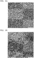
- FIGS. 2A and 2B show the structure observation pictures of the copper alloy materials of Example 2 of the present invention and Comparative Example 1, respectively, after the above-described aging treatment and before the heat treatment at 1000°C for 30 minutes retention.
- FIG. 3A and FIG. 3B show the structure observation pictures of the copper alloy materials of Example 2 of the present invention and Comparative Example 1, respectively, after the above-described aging treatment and the heat treatment at 1000°C for 30 minutes retention.
- the component composition of the obtained copper alloy material was measured by ICP-MS analysis. The measurement results are shown in Table 1.
- a sample of 10 mm ⁇ 15 mm from the central portion of the plate width was cut out from the obtained thickness of the copper alloy material and the surface in the rolling direction (RD direction) was polished and then micro etching was performed.
- FIGS. 4A to 4D show SEM-EPMA images of Example 2 of the present invention
- FIGS. 5A to 5C show SEM-EPMA images of Comparative Example 1.
- FIG. 6 shows an example of SEM-EPMA images (visual field of 250 ⁇ m ⁇ 250 ⁇ m) in calculating the area ratio of the Cu-Zr-P compound.
- a sample of 10 mm ⁇ 15 mm from the central portion of the plate width was cut out from the obtained thickness of the copper alloy material and the surface in the rolling direction (RD direction) was polished and then micro etching was performed.
- FIGS. 2A and 3A in Examples 1 to 6 of the present invention, grain coarsening was suppressed even after being placed in a high-temperature environment.
- Comparative Example 5 in which the area ratio of the Cr-Zr-P compound (phase) in a needle shape or a granular shape was less than the range of the scope of the present invention, and the tensile strength was significantly decreased after the heat treatment at 1000°C for 30 minutes.
- Examples 1-6 of the present invention electrical conductivity was high and there was no significant reduction of the tensile strength even after the heat treatment at 1000°C for 30 minutes.
- Examples 3-6 of the present invention in which the crystal grain size was set to 200 ⁇ m or less after the heat treatment at 1000°C for 30 minutes, the reduction of the tensile strength after the heat treatment at 1000°C for 30 minutes was suppressed.
Landscapes
- Chemical & Material Sciences (AREA)
- Engineering & Computer Science (AREA)
- Materials Engineering (AREA)
- Mechanical Engineering (AREA)
- Metallurgy (AREA)
- Organic Chemistry (AREA)
- Physics & Mathematics (AREA)
- Thermal Sciences (AREA)
- Crystallography & Structural Chemistry (AREA)
- Conductive Materials (AREA)
Abstract
Description
- The present invention relates to a copper alloy material suitable for a part used in a high temperature environment such as a molding material for casting and a welding part such as a contact tip.
- Priority is claimed on Japanese Patent Application No.
2015-219851, filed on November 9, 2015 - Conventionally, Cu-Cr-Zr-based alloys such as C18150 are used as a material for casting mold materials and welding members which are used at high temperatures, since they have excellent heat resistance and electrical conductivity as shown in Patent Literatures 1 to 3.
- These Cu-Cr-Zr-based alloy are usually produced by a production process, in which a cast made of Cu-Cr-Zr-based alloy is subjected to a plastic working; a solution treatment, for example in a condition of 950-1050°C of a retention temperature and 0.5-1.5 hours of a retention time, and an aging treatment, for example in a condition of 400-500°C of a retention temperature and 2-4 hours of a retention time, are performed on the plastically worked material; and then the material subjected to the solution and aging treatments is finished into a predetermined shape by machine working in the end. In addition, the solution treatment step in the Cu-Cr-Zr-based alloy can be carried out in combination with the plastic working step instead of the so-called in-line solution treatment. In that case, the solution treatment is performed concurrently with the hot rolling working.
- In the above-described Cu-Cr-Zr-based alloy, Cr and Zr are dissolved in the matrix of Cu by the solution treatment and fine precipitates of Cr and Zr are dispersed by the aging treatment to improve strength and conductivity.
-
- [PTL 1] Japanese Examined Patent Application, Second Publication No.
S62-182238(A - [PTL 2] Japanese Examined Patent Application, Second Publication No.
S62-182239(A - [PTL 3] Japanese Unexamined Patent Application, First Publication No.
H04-120438 - Although the above-described Cu-Cr-Zr-based alloy has excellent heat resistance, when it is exposed to a use environment with a peak temperature of 500°C or more, occasionally, re-solution of precipitate starts for the strength and the conductivity to be reduced and for coarsening of the crystal grain to occur.
- When coarsening of the crystal grains occurs, the propagation speed of the crack increases and the service life of the product may be shortened. In addition, there has been a problem that mechanical properties such as strength and elongation are remarkably deteriorated due to local occurrence of coarsening of crystal grains.
- The present invention has been made in view of the above-described circumstances. An object of the present invention to provide a copper alloy material which is capable of suppressing coarsening of crystal grains, is stable in characteristics and excellent in service life even when it is used in a high temperature environment of 500°C or more.
- To solve the above-described technical problem, an aspect of the present invention is directed to a copper alloy material having a composition including: 0.1 mass% or more and 1.5 mass% or less of Cr; 0.05 mass% or more and 0.25 mass% or less of Zr; 0.005 mass% or more and 0.10 mass% or less of P; and a Cu balance including inevitable impurities, wherein the copper alloy material includes a Cr-Zr-P compound containing Cr, Zr and P and an area ratio of the Cr-Zr-P compound is in a range of 0.5 % or more and 5.0 % or less in a structure observation, and the Cr-Zr-P compound is in a form of a needle shape or a granular shape and a length a longest side of the needle shape or the granular shape is 100µm or less (hereinafter, referred as "a copper alloy material of the present invention").
- In the copper alloy material as configured above, the composition includes 0.1 mass% or more and 1.5 mass% or less of Cr; 0.05 mass% or more and 0.25 mass% or less of Zr; 0.005 mass% or more and 0.10 mass% or less of P; and a Cu balance including inevitable impurities. Thus, by precipitating fine precipitates by the aging treatment, strength (hardness) and conductivity can be improved.
- In addition, in the copper alloy material of the present invention, the copper alloy material includes a Cr-Zr-P compound containing Cr, Zr and P and an area ratio of the Cr-Zr-P compound is in a range of 0.5 % or more and 5.0 % or less in a structure observation. Since the Cr-Zr-P compound containing Cr, Zr and P does not disappear even under a high temperature condition of about 1000°C, even when it is used in a high temperature environment, coarsening of crystal grains is suppressed by the grain boundary pinning effect of the Cr-Zr-P compound.
- In addition, the Cr-Zr-P compound is in a form of a needle shape or a granular shape and a length a longest side of the needle shape or the granular shape is 100µm or less. Thus, the above-described pinning effect can be obtained reliably.
- In the copper alloy material of the present invention, it is preferable that after performing a heat treatment at 1000°C for 30 minutes retention, an average size of crystal grains is 200 µm or less.
- In this case, even after performing the heat treatment at 1000°C for 30 minutes retention, crystal grains are not coarsened. Accordingly, mechanical properties and conductivity are stable even in a case of being used under high temperature condition at 500°C or more.
- In the copper alloy material of the present invention, it is preferable that the composition of the copper alloy material further includes Co in a range of 0.02 mass% or more and 0.15 mass% or less, and an atomic ratio of Co to P, [Co]/[P], is in a range of 0.5≤[Co]/[P]≤5.0.
- In this case, since the composition of the copper alloy material further includes Co in a range of 0.02 mass% or more and 0.15 mass% or less, CoP compounds and Co2P compounds exist in the copper alloy material to exhibit the grain boundary pinning effect with the above-described Cr-Zr-P compound. Accordingly, even when it is used in a high temperature environment, coarsening of crystal grains can be suppressed reliably.
- Further, since the atomic ratio of Co to P, [Co]/[P] is set to the range of 0.5≤[Co]/[P]≤5.0, solid-soluting of excessive Co and P can be suppressed. Accordingly, reduction of electrical conductivity can be suppressed.
- In addition, in the copper alloy material of the present invention containing Co, it is preferable that a total content of Ti and Hf in the inevitable impurities is 0.10 mass% or less.
- In this case, since the total content of Ti and Hf in the inevitable impurities is set to 0.10 mass% or less, the CoP compounds and the Co2P compounds are reliably formed. Accordingly, the grain boundary pinning effect can be exhibited effectively; and the coarsening of the crystal grains can be suppressed.
- According to the present invention, it is possible to provide a copper alloy material capable of suppressing coarsening of crystal grains and having stable characteristics and excellent service life even when it is used in a high temperature environment of 500°C or more.
-
-
FIG. 1 is a flowchart of a method of manufacturing a copper alloy material that is an embodiment of the present invention. -
FIG. 2A is a structural observation photograph of Example 2 of the present invention. -
FIG. 2B is a structural observation photograph of Comparative Example 1. -
FIG. 3A is a structure observation photograph of Example 2 of the present invention after performing the heat treatment at 1000°C for 30 minutes retention time. -
FIG. 3B is a structure observation photograph of Comparative Example 1 after performing the heat treatment at 1000°C for 30 minutes retention time. -
FIG. 4A is an SEM image in Example 2 of the present invention. -
FIG. 4B is an EPMA (Cr) image in Example 2 of the present invention. -
FIG. 4C is an EPMA (Zr) image in Example 2 of the present invention. -
FIG. 4D is an EPMA (P) image in Example 2 of the present invention. -
FIG. 5A is an SEM image in Comparative Example 1 of the present invention. -
FIG. 5B is an EPMA (Cr) image in Comparative Example 1 of the present invention. -
FIG. 5C is an EPMA (Zr) image in Comparative Example 1 of the present invention. -
FIG. 6 is an example of SEM-EPMA images in calculating the area ratio of the Cu-Zr-P compound. - Hereinafter, a copper alloy material is an embodiment of the present invention will be described.
- The copper alloy material of the present embodiment is a material for a part used in a high temperature environment such as a molding material for casting and a welding part.
- The copper alloy material according to the present embodiment has a composition including: 0.1 mass% or more and 1.5 mass% or less of Cr; 0.05 mass% or more and 0.25 mass% or less of Zr; 0.005 mass% or more and 0.10 mass% or less of P; and a Cu balance including inevitable impurities.
- The copper alloy material of the present embodiment may further include Co in the range of 0.02 mass% or more and 0.15 mass% or less; and the atomic ratio of Co to P, [Co]/[P], may be set in a range of 0.5≤[Co]/[P]≤5.0, as needed. In addition, in the case where Co is included, it is preferable that the total content of Ti and Hf in the inevitable impurities is set to 0.10 mass% or less.
- In addition, in the copper alloy material of the present embodiment, the copper alloy material includes a Cr-Zr-P compound (phase) containing Cr, Zr and P and an area ratio of the Cr-Zr-P compound (phase) is in a range of 0.5 % or more and 5.0 % or less in a structure observation, and the Cr-Zr-P compound is in a form of a needle shape or a granular shape and a length a longest side of the needle shape or the granular shape is 100µm or less.
- The "Cr-Zr-P compound (phase)" means a phase consisting of Cr-Zr-P compound wiht a constant content surrounded by grain boundaries.
- The "needle shape" means that the phase has an aspect ratio of 5 or more. The "granular shape" means the pahse has an aspect ratio of 1-3.
- The length of the longest side of the Cr-Zr-P compound (phase) in the needle shape can be obtained by measuring the length in the longitudinal direction of the needle shape.
- The length of the longest side of the Cr-Zr-P compound (phase) in the grain shaoe can be obtained by measuring the length of the granular shape in the direction in which the longest length can be obtained.
- The area ratio of the Cr-Zr-P compound (phase) is obtained by observing the structure of an arbitrary cross section of the copper alloy material (for example, a cross section parallel to the rolling direction) with SEM or the like after microscopic etching and further observing the cross section by performing element analysis with EPMA or the like.
- Furthermore, in the copper alloy material of the present embodiment, the average crystal grain sizes after heat treatment maintained at 1000°C for 30 minutes is set to 200 µm or less.
- The reasons why the composition of the copper alloy material according to the present embodiment, the crystal structure and the like are defined as described above will be described below.
- Cr is an element having an action effect that improves strength (hardness) and electrical conductivity by finely precipitating Cr-based precipitates in crystal grains of the parent phase by means of an aging treatment.
- Here, in a case where the content of Cr is less than 0.1 mass%, the precipitation amount during the aging treatment becomes insufficient, and there is a concern that the strength (hardness) improvement effect cannot be sufficiently obtained. In addition, in a case where the content of Cr exceeds 1.5 mass%, there is a concern that coarsened Cr crystalline materials are formed for workability to be reduced.
- On the basis of what has been described above, in the present embodiment, the content of Cr is set in a range of 0.1 mass% or more and 1.5 mass% or less. Meanwhile, in order to reliably exhibit the above-described action effect, the lower limit of the content of Cr is preferably set to 0.3 mass% or more, and the upper limit of the content of Cr is preferably set to 1.0 mass% or less.
- Zr is an element having an action effect that improves strength (hardness) and electrical conductivity by finely precipitating Zr-based precipitates in the crystal grain boundaries of the parent phase by means of the aging treatment.
- Here, in a case where the content of Zr is less than 0.05 mass%, the precipitation amount during the aging treatment becomes insufficient, and there is a concern that the strength (hardness) improvement effect cannot be sufficiently obtained. In addition, in a case where the content of Zr exceeds 0.25 mass%, there is a concern that electrical conductivity and thermal conductivity may decrease. In addition, even when more than 0.25 mass% of Zr is included, there is a concern that an additional strength improvement effect cannot be obtained.
- On the basis of what has been described above, in the present embodiment, the content of Zr is set in a range of 0.05 mass% or more and 0.25 mass% or less. Meanwhile, in order to reliably exhibit the above-described action effect, the lower limit of the content of Zr is preferably set to 0.07 mass% or more, and the upper limit of the content of Zr is preferably set to 0.15 mass% or less.
- By adding P to the Cu-Cr-Zr alloy, the Cr-Zr-P compound (phase) containing Cr, Zr and P is formed. Since the Cr-Zr-P compound (phase) does not disappear in a high temperature condition such as at 1000°C, addition of P exhibits the grain boundary pinning effect even when the alloy is used in a high temperature condition. Accordingly, coarsening of crystal grains can be suppressed.
- Here, in a case where the content of P is less than 0.005 mass%, there is a concern that the Cr-Zr-P compound (phase) is not formed. On the other hand, in a case where the content of P exceeds 0.10 mass%, there is a concern that the electrical conductivity may decrease and the pinning effect may not be exhibited sufficiently.
- On the basis of what has been described above, in the present embodiment, the content of P is set in a range of 0.005 mass% or more and 0.10 mass% or less. Meanwhile, in order to reliably exhibit the above-described action effect, the lower limit of the content of P is preferably set to 0.01 mass% or more, and the upper limit of the content of P is preferably set to 0.05 mass% or less.
- By adding Co, the CoP compound and the Co2P compounds are formed. The grain boundary pinning effect is exhibited by these the CoP compound and the Co2P compounds together with the above-described Cr-Zr-P compound (phase). Accordingly, coarsening of crystal grains are reliably suppressed even when the alloy is used in a high temperature condition.
- Here, in a case where the content of Co is less than 0.02 mass%, there is a concern that the CoP compound and the Co2P compounds are nor formed sufficiently and the pinning effect is not improved further even though Co is added. On the other hand, in a case where the content of Co exceeds 0.15 mass%, there is a concern that the CoP compound and the Co2P compounds are coarsened and the pinning effect is not improved further even though Co is added.
- On the basis of what has been described above, in the present embodiment, the content of Co is set in a range of 0.02 mass% or more and 0.15 mass% or less in a case where Co is included. Meanwhile, in order to reliably exhibit the above-described action effect, the lower limit of the content of Co is preferably set to 0.03 mass% or more, and the upper limit of the content of Co is preferably set to 0.1 mass% or less. In a case where Co is not added intentionally, less than 0.02 mass% of Co may be included as impurities.
- In a case where Co is added, the atomic ratio of Co to P, [Co]/[P] is set in the range of 0.5≤[Co]/[P]≤5.0. By setting the atomic ratio of Co to P, [Co]/[P] as described above, reduction of electrical conductivity due to solid-soluting of excessive Co and P, which do not contribute to fomation of the CoP compound and the Co2P compounds, in the matrix can be suppressed. Meanwhile, in order to reliably exhibit the above-described action effect, the lower limit of the atomic ratio of Co to P, [Co]/[P] is preferably set to 1.0 or more, and the upper limit of the atomic ratio of Co to P, [Co]/[P] is preferably set to 3.0 or less.
- Furthermore, in the case where Co is added, it is preferable that the total content of Ti and Hf which are inevitable impurities is set to 0.10 mass% or less. Since elements such as Ti and Hf are likely to form a compound with Co, there is a possibility that CoP compound and Co2P compound can not be formed sufficiently. Therefore, by setting the total content of inevitable impurities of Ti and Hf as described above, the CoP compound and the Co2P compound can be reliably formed and the pinning effect can be exhibited. In order to reliably exhibit the above-described action effect, it is preferable to set the total content of Ti and Hf as inevitable impurities to 0.03 mass% or less.
- Meanwhile, examples of the inevitable impurities other than Cr-Zr-P, Co, Ti, and Hf described above include B, Al, Fe, Sn, Zn, Si, Mg, Ag, Ca, Te, Mn, Ni, Sr, Ba, Sc , Y, Ti, Hf, V, Nb, Ta, Mo, W, Re, Ru, Os, Se, Rh, Ir, Pd, Pt, Au, Cd, Ga, In, Li, Ge, As, Sb, Tl, Pb, Be, N, H, Hg, Tc, Na, K, Rb, Cs, Po, Bi, lanthanoids, O, S, C and the like. Since there is a concern that these inevitable impurities may decrease the electrical conductivity and the thermal conductivity, the total amount thereof is preferably set to 0.05 mass% or less.
- In a case where the area ratio of the Cr-Zr-P compound (phase) is less than 0.5%, the crystal grain boundary pinning effect by the Cr-Zr-P compound (phase) becomes insufficient, and there is a concern that coarsening of crystal grains can not be suppressed. On the other hand, when the area ratio of the Cr-Zr-P compound (phase) exceeds 5.0%, there is a concern that workabiity is decreased.
- On the basis of what has been described above, in the present embodiment, the area ratio of the Cr-Zr-P compound (phase) is set to be 0.5% or more and 5.0% or less. It is preferable that the lower limit of the area ratio of the Cr-Zr-P compound (phase) is 1.0% or more, the upper limit of the area ratio of the Cr-Zr-P compound (phase) is 3.0% or less.
- In a case where the length as the longest side of the Cr-Cr-P compound (phase) in a needle shape or a granular shape exceeds 100 µm, there is a concern that the above-described pinning effect may not be exhibited sufficiently.
- On the basis of what has been described above, in the present embodiment, the length as the longest side of the Cr-Zr-P compound (phase) is set to 100 µm or less. It is preferable that the upper limit of the length as the longest side of the Cr-Zr-P compound (phase) is set to 80 µm or less.
- By setting the average crystal grain sizes after heat treatment at 1000°C for 30 minutes retension to 200 µm or less, coarsening of crystal grains can be suppressed reliably when the alloy is used in a high temperature condition such as at 500°C or more. Accordingly, properties such as strength are stabilized.
- On the basis of what has been described above, in the present embodiment, the average crystal grain sizes after heat treatment at 1000°C for 30 minutes retension is set to 200 µm or less.
- Next, a method for manufacturing the casting mold material according to the embodiment of the present invention will be described with reference to a flowchart of
FIG. 1 . - First, a copper raw material made of oxygen-free copper having a copper purity of 99.99 mass% or higher is loaded into a carbon crucible and is melted using a vacuum melting furnace, thereby obtaining molten copper. Next, the above-described additive elements are added to the obtained molten metal so as to obtain a predetermined concentration, and components are formulated, thereby obtaining a molten copper alloy.
- Here, as raw materials of Cr, Zr, and P which are the additive elements, Cr, and Zr having a high purity are used, and, for example, Cr having a purity of 99.99 mass% or higher is used as a raw material of Cr, Zr having a purity of 99.95 mass% or higher is used as a raw material of Zr, and P having a purity of 99.99 mass% or higher is used as a raw material of P. In addition, Co is added thereto as necessary. Meanwhile, as raw materials of Cr, Zr, Co and P, parent alloys with Cu may also be used.
- In addition, the component-formulated molten copper alloy is injected into a die, thereby obtaining an ingot.
- Next, a thermal treatment is carried out in order for the homogenization of the obtained ingot.
- Specifically, a homogenization treatment is carried out on the ingot in the atmosphere under conditions of 950°C or higher and 1,050°C or lower for one hour or longer.
- Next, hot rolling with a working percentage of 50% or higher and 99% or lower is carried out on the ingot in a temperature range of 900°C or higher and 1,000°C or lower, thereby obtaining a rolled material. Meanwhile, the method of the hot working may be hot forging. After this hot working, the rolled material is immediately cooled by means of water cooling.
- Next, a heating treatment is carried out on the rolled material obtained in the hot working step S03 under conditions of 920°C or higher and 1,050°C or lower for 0.5 hours or longer and five hours or shorter, thereby carrying out a solution treatment. The heating treatment is carried out, for example, in the atmosphere or an inert gas atmosphere, and as cooling after the heating, water cooling is carried out.
- Alternatively, by performing the inline solution treatment, the hot working step S03 and the solution treatment step S04 may be performed simultaneously.
- Specifically, hot rolling is performed with respect to the ingot at a reduction ratio of 50% or more and 99% or less in a temperature range of 900°C or more and 1000°C or less, and immediately from a temperature of 920°C or more and 1050°C or less, the solution treatment is performed.
- Next, after the solution treatment step S04, an aging treatment is carried out, and precipitates such as Cr-based precipitates and Zr-based precipitates are finely precipitated, thereby obtaining a aging treatment material.
- Here, the first aging treatment is carried out under conditions of, for example, 400°C or higher and 530°C or lower for 0.5 hours or longer and five hours or shorter.
- Meanwhile, the thermal treatment method during the aging treatment is not particularly limited, but the thermal treatment is preferably carried out in an inert gas atmosphere. In addition, the cooling method after the heating treatment is not particularly limited, but water cooling is preferably carried out.
- By means of the above-described steps, the copper alloy material that is the present embodiment is manufactured.
- According to the copper alloy material as configured to the above-described present embodiment, the copper alloy material has the composition including: 0.1 mass% or more and 1.5 mass% or less of Cr; 0.05 mass% or more and 0.25 mass% or less of Zr; 0.005 mass% or more and 0.10 mass% or less of P; and a Cu balance including inevitable impurities. Thus, by precipitating fine precipitates by the aging treatment, strength (hardness) and electrical conductivity can be improved.
- In addition, in the present embodiment, the copper alloy material includes a Cr-Zr-P compound containing Cr, Zr and P and an area ratio of the Cr-Zr-P compound is in a range of 0.5 % or more and 5.0 % or less in a structure observation. Thus, the Cr-Zr-P compound (phase) does not disappear even when it is used under a high temperature environment, and coarsening of crystal grains can be suppressed by the pinning effect of these Cr - Zr - P compound.
- In addition, in the present embodiment, the Cr-Zr-P compound is in a form of a needle shape or a grain shape and a length a longest side of the needle shape or the grain shape is 100µm or less. Thus, the above-described pinning effect can be obtained reliably.
- Moreover, in the present embodiment, since the average crystal grain sizes after heat treatment at 1000°C for 30 minutes retension is set to 200 µm or less. Thus, crystal grains are not coarsened and mechanical property and electrical conductivity are stabilized even when it is used in a high temperature environment of 500°C or more.
- In addition, in the present embodiment, in the case where Co is further included in the range of 0.02 mass% or more and 0.15 mass% or less, and the atomic ratio of Co to P, [Co]/[P] is 0.5≤[Co]/[P]≤5.0, the CoP compound and the Co2P compound are formed, and the crystal grain boundary pinning effect is exhibited together with the above Cr-Zr-P compound (phase). Accordingly, coarsening of crystal grains is suppressed reliably even when used under a high temperature environment. In addition, since the atomic ratio of Co to P, [Co]/[P] is set to 0.5≤[Co]/[P]≤5.0, solid-soluting of excessive Co and P can be suppressed. Accordingly, reduction of electrical conductivity can be suppressed.
- In addition, in the case where the composition of the copper alloy material further includes Co, by setting the total content of Ti and Hf in the inevitable impurities to 0.10 mass% or less, the CoP compounds and the Co2P compounds are reliably formed. Accordingly, the grain boundary pinning effect can be exhibited effectively; and the coarsening of the crystal grains can be suppressed.
- Hitherto, the embodiment of the present invention has been described, but the present invention is not limited thereto and can be appropriately modified in the scope of the technical concept of the invention.
- Hereinafter, the results of confirmation tests carried out in order to confirm the effects of the present invention will be described.
- A copper raw material made of oxygen-free copper having a copper purity of 99.99 mass% or higher was prepared, was loaded into a carbon crucible, and was melted using a vacuum melting furnace (with a degree of vacuum of 10-2 Pa or lower), thereby obtaining molten copper. A variety of additive elements were added to the obtained molten copper so as to formulate a component composition shown in Table 1, the component composition was maintained for five minutes, and then the molten copper alloy was injected into a cast iron die, thereby obtaining an ingot. The sizes of the ingot were set to a width of approximately 80 mm, a thickness of approximately 50 mm, and a length of approximately 130 mm.
- Meanwhile, as a raw material of Cr which was an additive element, Cr having a purity of 99.99 mass% or higher was used, and as a raw material of Zr, Zr having a purity of 99.95 mass% or higher was used, was used.
- Next, a homogenization treatment was carried out in the atmosphere under conditions of 1,000°C for one hour, and then hot rolling was carried out. The rolling reduction in the hot rolling was set to 80%, thereby obtaining a hot-rolled material having a width of approximately 100 mm, a thickness of approximately 10 mm, and a length of approximately 520 mm.
- In the present Examples, the cooling at the cooling rates shown in Table 1 performed after the end of the hot rolling functioned as the solution treatment as well. In other words, the so-called inline solution treatment was performed.
- Next, a aging treatment was carried out under conditions of 500 (±15)°C for three hours. By following above-described procedures, the copper alloy materials were obtained.
- For the obtained copper alloy material, the structure of the copper alloy material after the aging treatment was observed, and the Cr-Zr-P compound (phase) was evaluated. In addition, the electrical conductivity and the tensile strength of the copper alloy materials after the aging treatment were measured.
- In addition, the heat treatment at 1000°C for 30 minutes retention was performed on the copper alloy materials after the aging treatment; and after water cooling these copper alloy materials, the average crystal grain sizes and the tensile strength were measured.
-
FIGS. 2A and 2B show the structure observation pictures of the copper alloy materials of Example 2 of the present invention and Comparative Example 1, respectively, after the above-described aging treatment and before the heat treatment at 1000°C for 30 minutes retention. - Similarly,
FIG. 3A and FIG. 3B show the structure observation pictures of the copper alloy materials of Example 2 of the present invention and Comparative Example 1, respectively, after the above-described aging treatment and the heat treatment at 1000°C for 30 minutes retention. - The component composition of the obtained copper alloy material was measured by ICP-MS analysis. The measurement results are shown in Table 1.
- A sample of 10 mm × 15 mm from the central portion of the plate width was cut out from the obtained thickness of the copper alloy material and the surface in the rolling direction (RD direction) was polished and then micro etching was performed.
- The sample was observed by SEM. In the SEM-EPMA image (field of view of 250 µm × 250 µm), the region where the Cr, Zr, and P concentrations were higher than that of the matrix phase was defined as "Cr-Zr-P compound (phase)." Then, the length of the longest side was measured. Then, the area ratio of the Cu-Zr-P compound was determined by the following formula.

-
FIGS. 4A to 4D show SEM-EPMA images of Example 2 of the present invention, andFIGS. 5A to 5C show SEM-EPMA images of Comparative Example 1. In addition,FIG. 6 shows an example of SEM-EPMA images (visual field of 250 µm × 250 µm) in calculating the area ratio of the Cu-Zr-P compound. - A sample of 10 mm × 15 mm from the central portion of the plate width was cut out from the obtained thickness of the copper alloy material and the surface in the rolling direction (RD direction) was polished and then micro etching was performed.
- This sample was observed and the average crystal grain size was measured by the intercept method prescribed in JIS H 0501.
- Using a SIGMA TEST D 2.068 (probe diameter ϕ 6 mm) manufactured by Nippon Felster Co., Ltd., the cross section center portion of a sample of 10 × 15 mm was measured three times, and the average value thereof was obtained.
- JIS Z 2241 No. 2 test piece was taken with the rolling direction as the pulling direction and subjected to the test using a 100 kN tensile tester.
[Table 1] Composition (mass%) [Co]/[P] Cooling rate after the solution treatment (°C/min) Cr Zr P Co Ti Hf Cu Example of the present invention 1 0.35 0.14 0.02 - - - balance 0.0 31 2 0.40 0.14 0.02 0.06 - - balance 3.0 1000 3 0.55 0.07 0.02 - - - balance 0.0 1000 4 1.00 0.08 0.09 - - - balance 0.0 1000 5 1.40 0.08 0.05 0.03 - - balance 0.6 1000 6 0.90 0.19 0.03 0.14 - - balance 4.7 1000 Comparative Example 1 0.70 0.06 - - - - balance - 1000 2 1.50 0.23 0.08 - - - balance 0.0 13 3 0.70 0.60 0.06 - - - balance 0.0 800 4 1.00 0.09 0.03 0.18 - - balance 6.0 800 5 0.40 0.14 0.04 0.15 0.10 0.11 balance 3.75 1000 [Table 2] Cr-Zr-P compound in a needle shape or a granular shape Electrical conductivity (%IACS) Tensile strength after the aging treatment (MPa) After the heat treatment at 1000°C for 30 minutes retention Presence or Absence Length of the longest side (µm) Area ratio (%) Average size of crystal grains (µm) Tensile strength (MPa) Example of the present invention 1 Present 20 1.20 77.0 435 280 398 2 Present 25 0.80 75.0 430 263 412 3 Present 24 1.20 82.0 435 78 424 4 Present 35 1.40 79.0 443 39 401 5 Present 51 3.10 83.0 461 51 433 6 Present 74 4.50 72.0 452 43 427 Comparative Example 1 Absent - - 87.0 434 870 341 2 Present - 6.50 77.0 463 530 378 3 Present 160 2.30 63.0 438 510 388 4 Present 27 0.60 65.0 451 125 412 5 Present 22 0.10 73.0 442 610 361 -
FIGS. 2A and3A , in Examples 1 to 6 of the present invention, grain coarsening was suppressed even after being placed in a high-temperature environment. - On the other hand, as shown in
FIGS. 2B and3B , in Comparative Examples 1 to 3 and 5, the crystal grains coarsened after being placed in a high-temperature environment. In Comparative Example 4, coarsening of crystal grains was not observed, but the conductivity was lower than that of Examples 1 to 6 of the present invention (described later). - In Comparative Example 1 in which P was not added, Cr-Zr-P compounds (phases) in a needle shape or a granular shape were not produced, so that the tensile strength significantly decreased after the heat treatment at 1000°C for 30 minutes.
- In Comparative Example 2 in which the area ratio of the Cr-Zr-P compound (phase) in a needle shape or a granular shape exceeded the range of the scope of the present invention; and the tensile strength significantly decreased after the heat treatment at 1000 °C for 30 minutes.
- In Comparative Example 3 in which the content of Zr exceeded the scope of the range of the present invention, the electrical conductivity was low and the tensile strength was significantly decreased after the heat treatment at 1000°C for 30 minutes.
- In Comparative Example 4 in which the content of Co exceeded the scope of the range of the present invention, the conductivity was low.
- In Comparative Example 5 in which the area ratio of the Cr-Zr-P compound (phase) in a needle shape or a granular shape was less than the range of the scope of the present invention, and the tensile strength was significantly decreased after the heat treatment at 1000°C for 30 minutes.
- In contrast, in Examples 1-6 of the present invention, electrical conductivity was high and there was no significant reduction of the tensile strength even after the heat treatment at 1000°C for 30 minutes. In addition, in Examples 3-6 of the present invention, in which the crystal grain size was set to 200 µm or less after the heat treatment at 1000°C for 30 minutes, the reduction of the tensile strength after the heat treatment at 1000°C for 30 minutes was suppressed.
- From the above-described results, according to the example of the present invention, it is confirmed that a copper alloy material capable of suppressing coarsening of crystal grains and having stable properties and excellent service life even when it is used under a high temperature environment of 500°C or more was provided.
- It is possible to suppress property deterioration of a part made of the Cu-Cr-Zr-based alloy in a high temperature environment and prolong the service life of the casting molding material, the welding part and the like.
Claims (4)
- A copper alloy material having a composition including:0.1 mass% or more and 1.5 mass% or less of Cr;0.05 mass% or more and 0.25 mass% or less of Zr;0.005 mass% or more and 0.10 mass% or less of P; anda Cu balance including inevitable impurities,wherein the copper alloy material includes a Cr-Zr-P compound containing Cr, Zr and P and an area ratio of the Cr-Zr-P compound is in a range of 0.5 % or more and 5.0 % or less in a structure observation, andthe Cr-Zr-P compound is in a form of a needle shape or a granular shape and a length a longest side of the needle shape or the granular shape is 100µm or less.
- The copper alloy material according to Claim 1,
wherein, after performing a heat treatment at 1000°C for 30 minutes retention, an average size of crystal grains is 200 µm or less. - The copper alloy material according to Claim 1 or 2,
wherein, the composition of the copper alloy material further includes Co in a range of 0.02 mass% or more and 0.15 mass% or less, and
an atomic ratio of Co to P, [Co]/[P], is in a range of 0.5≤[Co]/[P]≤5.0. - The copper alloy material according to Claim 3, wherein a total content of Ti and Hf in the inevitable impurities is 0.10 mass% or less.
Applications Claiming Priority (2)
| Application Number | Priority Date | Filing Date | Title |
|---|---|---|---|
| JP2015219851A JP6736869B2 (en) | 2015-11-09 | 2015-11-09 | Copper alloy material |
| PCT/JP2016/080082 WO2017081969A1 (en) | 2015-11-09 | 2016-10-11 | Copper alloy material |
Publications (3)
| Publication Number | Publication Date |
|---|---|
| EP3375897A1 true EP3375897A1 (en) | 2018-09-19 |
| EP3375897A4 EP3375897A4 (en) | 2019-04-03 |
| EP3375897B1 EP3375897B1 (en) | 2021-09-01 |
Family
ID=58695038
Family Applications (1)
| Application Number | Title | Priority Date | Filing Date |
|---|---|---|---|
| EP16863933.4A Active EP3375897B1 (en) | 2015-11-09 | 2016-10-11 | Copper alloy material |
Country Status (6)
| Country | Link |
|---|---|
| US (1) | US20180291490A1 (en) |
| EP (1) | EP3375897B1 (en) |
| JP (1) | JP6736869B2 (en) |
| KR (1) | KR102493118B1 (en) |
| CN (1) | CN108291275B (en) |
| WO (1) | WO2017081969A1 (en) |
Families Citing this family (4)
| Publication number | Priority date | Publication date | Assignee | Title |
|---|---|---|---|---|
| JP6488951B2 (en) * | 2014-09-25 | 2019-03-27 | 三菱マテリアル株式会社 | Mold material for casting and Cu-Cr-Zr alloy material |
| JP7035478B2 (en) * | 2017-11-21 | 2022-03-15 | 三菱マテリアル株式会社 | Molding material for casting |
| JP2020133000A (en) * | 2019-02-20 | 2020-08-31 | 三菱マテリアル株式会社 | Copper alloy material, commutator piece, electrode material |
| CN115612888A (en) * | 2022-09-26 | 2023-01-17 | 陕西科技大学 | Heat-shock-resistant copper alloy material for rocket engine and preparation method thereof |
Family Cites Families (17)
| Publication number | Priority date | Publication date | Assignee | Title |
|---|---|---|---|---|
| JP2614210B2 (en) | 1986-02-06 | 1997-05-28 | 三菱マテリアル株式会社 | Cu alloy for continuous casting mold |
| JPH07113133B2 (en) | 1986-02-06 | 1995-12-06 | 三菱マテリアル株式会社 | Cu alloy for continuous casting mold |
| JPS63143229A (en) * | 1986-12-08 | 1988-06-15 | Nippon Mining Co Ltd | Copper alloy having superior castability |
| JPH01309935A (en) * | 1988-06-07 | 1989-12-14 | Kobe Steel Ltd | Copper alloy for hot scarfing nozzle unit of steel |
| JPH04210438A (en) | 1990-12-13 | 1992-07-31 | Mitsubishi Materials Corp | Continuous casting mold material made of high strength cu alloy |
| JPH0570867A (en) * | 1991-06-25 | 1993-03-23 | Mitsubishi Materials Corp | Casting method and casting die alloy |
| JPH05339688A (en) * | 1992-06-05 | 1993-12-21 | Furukawa Electric Co Ltd:The | Production of molding material for casting metal |
| JP3699701B2 (en) * | 2002-10-31 | 2005-09-28 | 日鉱金属加工株式会社 | Easy-to-process high-strength, high-conductivity copper alloy |
| JP4087307B2 (en) * | 2003-07-09 | 2008-05-21 | 日鉱金属株式会社 | High strength and high conductivity copper alloy with excellent ductility |
| US20060088437A1 (en) * | 2004-10-22 | 2006-04-27 | Russell Nippert | Copper based precipitation hardening alloy |
| WO2010079707A1 (en) * | 2009-01-09 | 2010-07-15 | 三菱伸銅株式会社 | High-strength high-conductivity copper alloy rolled sheet and method for producing same |
| EP2610358A4 (en) * | 2010-08-27 | 2017-05-03 | Furukawa Electric Co., Ltd. | Copper alloy sheet and manufacturing method for same |
| EP2610359A4 (en) * | 2010-08-27 | 2017-08-02 | Furukawa Electric Co., Ltd. | Copper alloy sheet and method for producing same |
| JP5712585B2 (en) * | 2010-12-03 | 2015-05-07 | 三菱マテリアル株式会社 | Copper alloy for electronic equipment, method for producing copper alloy for electronic equipment, and rolled copper alloy material for electronic equipment |
| US20140096877A1 (en) * | 2011-06-06 | 2014-04-10 | Mitsubishi Materials Corporation | Copper alloy for electronic devices, method for producing copper alloy for electronic devices, copper alloy plastic working material for electronic devices, and component for electronic devices |
| KR101364542B1 (en) * | 2011-08-11 | 2014-02-18 | 주식회사 풍산 | Copper alloy material for continuous casting mold and process of production same |
| CN102912178B (en) * | 2012-09-29 | 2015-08-19 | 河南科技大学 | A kind of high-strength highly-conductive rare-earth copper alloy and preparation method thereof |
-
2015
- 2015-11-09 JP JP2015219851A patent/JP6736869B2/en active Active
-
2016
- 2016-10-11 CN CN201680065120.7A patent/CN108291275B/en active Active
- 2016-10-11 US US15/769,024 patent/US20180291490A1/en not_active Abandoned
- 2016-10-11 EP EP16863933.4A patent/EP3375897B1/en active Active
- 2016-10-11 WO PCT/JP2016/080082 patent/WO2017081969A1/en not_active Ceased
- 2016-10-11 KR KR1020187012110A patent/KR102493118B1/en active Active
Also Published As
| Publication number | Publication date |
|---|---|
| EP3375897B1 (en) | 2021-09-01 |
| JP2017088948A (en) | 2017-05-25 |
| EP3375897A4 (en) | 2019-04-03 |
| KR102493118B1 (en) | 2023-01-27 |
| US20180291490A1 (en) | 2018-10-11 |
| WO2017081969A1 (en) | 2017-05-18 |
| CN108291275A (en) | 2018-07-17 |
| KR20180078244A (en) | 2018-07-09 |
| CN108291275B (en) | 2020-03-13 |
| JP6736869B2 (en) | 2020-08-05 |
Similar Documents
| Publication | Publication Date | Title |
|---|---|---|
| JP5045784B2 (en) | Copper alloy for electronic equipment, method for producing copper alloy for electronic equipment, and rolled copper alloy material for electronic equipment | |
| EP3040430B1 (en) | Copper alloy sheet material and method for producing same, and current-carrying component | |
| JP5712585B2 (en) | Copper alloy for electronic equipment, method for producing copper alloy for electronic equipment, and rolled copper alloy material for electronic equipment | |
| EP3375898B1 (en) | Copper alloy material | |
| EP2570506B1 (en) | Copper alloy for electronic device, method for producing this alloy, and copper alloy rolled material for this device | |
| TWI513833B (en) | Copper alloy for electronic device, method for manufacturing copper alloy for electronic device, wrought copper alloy material for electronic device, and part for electronic device | |
| JP4834781B1 (en) | Cu-Co-Si alloy for electronic materials | |
| TWI429768B (en) | Cu-Co-Si based copper alloy for electronic materials and method for producing the same | |
| JP2011241412A (en) | Copper alloy for electronic device, method for producing copper alloy for electronic device and copper alloy rolled material for electronic device | |
| EP3199651B1 (en) | Casting mold material made of a cu-cr-zr alloy and method for manufacturing it | |
| KR20120130342A (en) | Cu-ni-si alloy for electronic material | |
| EP3375897B1 (en) | Copper alloy material | |
| EP3363921B1 (en) | Casting mold material and cu-cr-zr-al alloy starting material | |
| EP3715488A1 (en) | Mold material for casting and copper alloy material | |
| JP2011241411A (en) | Copper alloy for electronic device, method for producing copper alloy for electronic device and copper alloy rolled material for electronic device | |
| JP2013117060A (en) | Cu-Co-Si-BASED ALLOY FOR ELECTRONIC MATERIAL |
Legal Events
| Date | Code | Title | Description |
|---|---|---|---|
| STAA | Information on the status of an ep patent application or granted ep patent |
Free format text: STATUS: THE INTERNATIONAL PUBLICATION HAS BEEN MADE |
|
| PUAI | Public reference made under article 153(3) epc to a published international application that has entered the european phase |
Free format text: ORIGINAL CODE: 0009012 |
|
| STAA | Information on the status of an ep patent application or granted ep patent |
Free format text: STATUS: REQUEST FOR EXAMINATION WAS MADE |
|
| 17P | Request for examination filed |
Effective date: 20180416 |
|
| AK | Designated contracting states |
Kind code of ref document: A1 Designated state(s): AL AT BE BG CH CY CZ DE DK EE ES FI FR GB GR HR HU IE IS IT LI LT LU LV MC MK MT NL NO PL PT RO RS SE SI SK SM TR |
|
| AX | Request for extension of the european patent |
Extension state: BA ME |
|
| DAV | Request for validation of the european patent (deleted) | ||
| DAX | Request for extension of the european patent (deleted) | ||
| A4 | Supplementary search report drawn up and despatched |
Effective date: 20190306 |
|
| RIC1 | Information provided on ipc code assigned before grant |
Ipc: C22C 9/00 20060101AFI20190227BHEP Ipc: C22F 1/08 20060101ALI20190227BHEP |
|
| RAP1 | Party data changed (applicant data changed or rights of an application transferred) |
Owner name: MITSUBISHI MATERIALS CORPORATION |
|
| STAA | Information on the status of an ep patent application or granted ep patent |
Free format text: STATUS: EXAMINATION IS IN PROGRESS |
|
| 17Q | First examination report despatched |
Effective date: 20190917 |
|
| GRAP | Despatch of communication of intention to grant a patent |
Free format text: ORIGINAL CODE: EPIDOSNIGR1 |
|
| STAA | Information on the status of an ep patent application or granted ep patent |
Free format text: STATUS: GRANT OF PATENT IS INTENDED |
|
| INTG | Intention to grant announced |
Effective date: 20210211 |
|
| RIN1 | Information on inventor provided before grant (corrected) |
Inventor name: SAKAMOTO, TOSHIO Inventor name: SATOU, SHINOBU Inventor name: YANO, SHOICHIRO |
|
| GRAJ | Information related to disapproval of communication of intention to grant by the applicant or resumption of examination proceedings by the epo deleted |
Free format text: ORIGINAL CODE: EPIDOSDIGR1 |
|
| STAA | Information on the status of an ep patent application or granted ep patent |
Free format text: STATUS: EXAMINATION IS IN PROGRESS |
|
| INTC | Intention to grant announced (deleted) | ||
| GRAP | Despatch of communication of intention to grant a patent |
Free format text: ORIGINAL CODE: EPIDOSNIGR1 |
|
| STAA | Information on the status of an ep patent application or granted ep patent |
Free format text: STATUS: GRANT OF PATENT IS INTENDED |
|
| INTG | Intention to grant announced |
Effective date: 20210617 |
|
| GRAS | Grant fee paid |
Free format text: ORIGINAL CODE: EPIDOSNIGR3 |
|
| GRAA | (expected) grant |
Free format text: ORIGINAL CODE: 0009210 |
|
| STAA | Information on the status of an ep patent application or granted ep patent |
Free format text: STATUS: THE PATENT HAS BEEN GRANTED |
|
| AK | Designated contracting states |
Kind code of ref document: B1 Designated state(s): AL AT BE BG CH CY CZ DE DK EE ES FI FR GB GR HR HU IE IS IT LI LT LU LV MC MK MT NL NO PL PT RO RS SE SI SK SM TR |
|
| REG | Reference to a national code |
Ref country code: GB Ref legal event code: FG4D |
|
| REG | Reference to a national code |
Ref country code: CH Ref legal event code: EP Ref country code: AT Ref legal event code: REF Ref document number: 1426327 Country of ref document: AT Kind code of ref document: T Effective date: 20210915 |
|
| REG | Reference to a national code |
Ref country code: DE Ref legal event code: R096 Ref document number: 602016063264 Country of ref document: DE |
|
| REG | Reference to a national code |
Ref country code: IE Ref legal event code: FG4D |
|
| REG | Reference to a national code |
Ref country code: LT Ref legal event code: MG9D |
|
| REG | Reference to a national code |
Ref country code: NL Ref legal event code: MP Effective date: 20210901 |
|
| PG25 | Lapsed in a contracting state [announced via postgrant information from national office to epo] |
Ref country code: LT Free format text: LAPSE BECAUSE OF FAILURE TO SUBMIT A TRANSLATION OF THE DESCRIPTION OR TO PAY THE FEE WITHIN THE PRESCRIBED TIME-LIMIT Effective date: 20210901 Ref country code: BG Free format text: LAPSE BECAUSE OF FAILURE TO SUBMIT A TRANSLATION OF THE DESCRIPTION OR TO PAY THE FEE WITHIN THE PRESCRIBED TIME-LIMIT Effective date: 20211201 Ref country code: HR Free format text: LAPSE BECAUSE OF FAILURE TO SUBMIT A TRANSLATION OF THE DESCRIPTION OR TO PAY THE FEE WITHIN THE PRESCRIBED TIME-LIMIT Effective date: 20210901 Ref country code: ES Free format text: LAPSE BECAUSE OF FAILURE TO SUBMIT A TRANSLATION OF THE DESCRIPTION OR TO PAY THE FEE WITHIN THE PRESCRIBED TIME-LIMIT Effective date: 20210901 Ref country code: FI Free format text: LAPSE BECAUSE OF FAILURE TO SUBMIT A TRANSLATION OF THE DESCRIPTION OR TO PAY THE FEE WITHIN THE PRESCRIBED TIME-LIMIT Effective date: 20210901 Ref country code: NO Free format text: LAPSE BECAUSE OF FAILURE TO SUBMIT A TRANSLATION OF THE DESCRIPTION OR TO PAY THE FEE WITHIN THE PRESCRIBED TIME-LIMIT Effective date: 20211201 Ref country code: RS Free format text: LAPSE BECAUSE OF FAILURE TO SUBMIT A TRANSLATION OF THE DESCRIPTION OR TO PAY THE FEE WITHIN THE PRESCRIBED TIME-LIMIT Effective date: 20210901 Ref country code: SE Free format text: LAPSE BECAUSE OF FAILURE TO SUBMIT A TRANSLATION OF THE DESCRIPTION OR TO PAY THE FEE WITHIN THE PRESCRIBED TIME-LIMIT Effective date: 20210901 |
|
| PG25 | Lapsed in a contracting state [announced via postgrant information from national office to epo] |
Ref country code: PL Free format text: LAPSE BECAUSE OF FAILURE TO SUBMIT A TRANSLATION OF THE DESCRIPTION OR TO PAY THE FEE WITHIN THE PRESCRIBED TIME-LIMIT Effective date: 20210901 Ref country code: LV Free format text: LAPSE BECAUSE OF FAILURE TO SUBMIT A TRANSLATION OF THE DESCRIPTION OR TO PAY THE FEE WITHIN THE PRESCRIBED TIME-LIMIT Effective date: 20210901 Ref country code: GR Free format text: LAPSE BECAUSE OF FAILURE TO SUBMIT A TRANSLATION OF THE DESCRIPTION OR TO PAY THE FEE WITHIN THE PRESCRIBED TIME-LIMIT Effective date: 20211202 |
|
| REG | Reference to a national code |
Ref country code: CH Ref legal event code: PL |
|
| PG25 | Lapsed in a contracting state [announced via postgrant information from national office to epo] |
Ref country code: IS Free format text: LAPSE BECAUSE OF FAILURE TO SUBMIT A TRANSLATION OF THE DESCRIPTION OR TO PAY THE FEE WITHIN THE PRESCRIBED TIME-LIMIT Effective date: 20220101 Ref country code: SM Free format text: LAPSE BECAUSE OF FAILURE TO SUBMIT A TRANSLATION OF THE DESCRIPTION OR TO PAY THE FEE WITHIN THE PRESCRIBED TIME-LIMIT Effective date: 20210901 Ref country code: SK Free format text: LAPSE BECAUSE OF FAILURE TO SUBMIT A TRANSLATION OF THE DESCRIPTION OR TO PAY THE FEE WITHIN THE PRESCRIBED TIME-LIMIT Effective date: 20210901 Ref country code: RO Free format text: LAPSE BECAUSE OF FAILURE TO SUBMIT A TRANSLATION OF THE DESCRIPTION OR TO PAY THE FEE WITHIN THE PRESCRIBED TIME-LIMIT Effective date: 20210901 Ref country code: PT Free format text: LAPSE BECAUSE OF FAILURE TO SUBMIT A TRANSLATION OF THE DESCRIPTION OR TO PAY THE FEE WITHIN THE PRESCRIBED TIME-LIMIT Effective date: 20220103 Ref country code: NL Free format text: LAPSE BECAUSE OF FAILURE TO SUBMIT A TRANSLATION OF THE DESCRIPTION OR TO PAY THE FEE WITHIN THE PRESCRIBED TIME-LIMIT Effective date: 20210901 Ref country code: EE Free format text: LAPSE BECAUSE OF FAILURE TO SUBMIT A TRANSLATION OF THE DESCRIPTION OR TO PAY THE FEE WITHIN THE PRESCRIBED TIME-LIMIT Effective date: 20210901 Ref country code: CZ Free format text: LAPSE BECAUSE OF FAILURE TO SUBMIT A TRANSLATION OF THE DESCRIPTION OR TO PAY THE FEE WITHIN THE PRESCRIBED TIME-LIMIT Effective date: 20210901 Ref country code: AL Free format text: LAPSE BECAUSE OF FAILURE TO SUBMIT A TRANSLATION OF THE DESCRIPTION OR TO PAY THE FEE WITHIN THE PRESCRIBED TIME-LIMIT Effective date: 20210901 |
|
| REG | Reference to a national code |
Ref country code: DE Ref legal event code: R097 Ref document number: 602016063264 Country of ref document: DE |
|
| REG | Reference to a national code |
Ref country code: BE Ref legal event code: MM Effective date: 20211031 |
|
| PG25 | Lapsed in a contracting state [announced via postgrant information from national office to epo] |
Ref country code: MC Free format text: LAPSE BECAUSE OF FAILURE TO SUBMIT A TRANSLATION OF THE DESCRIPTION OR TO PAY THE FEE WITHIN THE PRESCRIBED TIME-LIMIT Effective date: 20210901 |
|
| PLBE | No opposition filed within time limit |
Free format text: ORIGINAL CODE: 0009261 |
|
| STAA | Information on the status of an ep patent application or granted ep patent |
Free format text: STATUS: NO OPPOSITION FILED WITHIN TIME LIMIT |
|
| PG25 | Lapsed in a contracting state [announced via postgrant information from national office to epo] |
Ref country code: LU Free format text: LAPSE BECAUSE OF NON-PAYMENT OF DUE FEES Effective date: 20211011 Ref country code: DK Free format text: LAPSE BECAUSE OF FAILURE TO SUBMIT A TRANSLATION OF THE DESCRIPTION OR TO PAY THE FEE WITHIN THE PRESCRIBED TIME-LIMIT Effective date: 20210901 Ref country code: BE Free format text: LAPSE BECAUSE OF NON-PAYMENT OF DUE FEES Effective date: 20211031 |
|
| 26N | No opposition filed |
Effective date: 20220602 |
|
| PG25 | Lapsed in a contracting state [announced via postgrant information from national office to epo] |
Ref country code: SI Free format text: LAPSE BECAUSE OF FAILURE TO SUBMIT A TRANSLATION OF THE DESCRIPTION OR TO PAY THE FEE WITHIN THE PRESCRIBED TIME-LIMIT Effective date: 20210901 Ref country code: LI Free format text: LAPSE BECAUSE OF NON-PAYMENT OF DUE FEES Effective date: 20211031 Ref country code: CH Free format text: LAPSE BECAUSE OF NON-PAYMENT OF DUE FEES Effective date: 20211031 |
|
| PG25 | Lapsed in a contracting state [announced via postgrant information from national office to epo] |
Ref country code: IE Free format text: LAPSE BECAUSE OF NON-PAYMENT OF DUE FEES Effective date: 20211011 |
|
| REG | Reference to a national code |
Ref country code: AT Ref legal event code: UEP Ref document number: 1426327 Country of ref document: AT Kind code of ref document: T Effective date: 20210901 |
|
| PG25 | Lapsed in a contracting state [announced via postgrant information from national office to epo] |
Ref country code: HU Free format text: LAPSE BECAUSE OF FAILURE TO SUBMIT A TRANSLATION OF THE DESCRIPTION OR TO PAY THE FEE WITHIN THE PRESCRIBED TIME-LIMIT; INVALID AB INITIO Effective date: 20161011 |
|
| PG25 | Lapsed in a contracting state [announced via postgrant information from national office to epo] |
Ref country code: CY Free format text: LAPSE BECAUSE OF FAILURE TO SUBMIT A TRANSLATION OF THE DESCRIPTION OR TO PAY THE FEE WITHIN THE PRESCRIBED TIME-LIMIT Effective date: 20210901 |
|
| PG25 | Lapsed in a contracting state [announced via postgrant information from national office to epo] |
Ref country code: MK Free format text: LAPSE BECAUSE OF FAILURE TO SUBMIT A TRANSLATION OF THE DESCRIPTION OR TO PAY THE FEE WITHIN THE PRESCRIBED TIME-LIMIT Effective date: 20210901 |
|
| PG25 | Lapsed in a contracting state [announced via postgrant information from national office to epo] |
Ref country code: MT Free format text: LAPSE BECAUSE OF FAILURE TO SUBMIT A TRANSLATION OF THE DESCRIPTION OR TO PAY THE FEE WITHIN THE PRESCRIBED TIME-LIMIT Effective date: 20210901 |
|
| PG25 | Lapsed in a contracting state [announced via postgrant information from national office to epo] |
Ref country code: TR Free format text: LAPSE BECAUSE OF FAILURE TO SUBMIT A TRANSLATION OF THE DESCRIPTION OR TO PAY THE FEE WITHIN THE PRESCRIBED TIME-LIMIT Effective date: 20210901 |
|
| PGFP | Annual fee paid to national office [announced via postgrant information from national office to epo] |
Ref country code: DE Payment date: 20251021 Year of fee payment: 10 |
|
| PGFP | Annual fee paid to national office [announced via postgrant information from national office to epo] |
Ref country code: GB Payment date: 20251022 Year of fee payment: 10 |
|
| PGFP | Annual fee paid to national office [announced via postgrant information from national office to epo] |
Ref country code: AT Payment date: 20251022 Year of fee payment: 10 |
|
| PGFP | Annual fee paid to national office [announced via postgrant information from national office to epo] |
Ref country code: IT Payment date: 20251024 Year of fee payment: 10 |
|
| PGFP | Annual fee paid to national office [announced via postgrant information from national office to epo] |
Ref country code: FR Payment date: 20251030 Year of fee payment: 10 |