EP3373053A1 - Regulierungsverfahren der parallelität eines faserblocks mit einer chip-oberfläche - Google Patents
Regulierungsverfahren der parallelität eines faserblocks mit einer chip-oberfläche Download PDFInfo
- Publication number
- EP3373053A1 EP3373053A1 EP18160425.7A EP18160425A EP3373053A1 EP 3373053 A1 EP3373053 A1 EP 3373053A1 EP 18160425 A EP18160425 A EP 18160425A EP 3373053 A1 EP3373053 A1 EP 3373053A1
- Authority
- EP
- European Patent Office
- Prior art keywords
- block
- sensor
- face
- point
- distance
- Prior art date
- Legal status (The legal status is an assumption and is not a legal conclusion. Google has not performed a legal analysis and makes no representation as to the accuracy of the status listed.)
- Granted
Links
Images

Classifications
-
- G—PHYSICS
- G02—OPTICS
- G02B—OPTICAL ELEMENTS, SYSTEMS OR APPARATUS
- G02B6/00—Light guides; Structural details of arrangements comprising light guides and other optical elements, e.g. couplings
- G02B6/24—Coupling light guides
- G02B6/42—Coupling light guides with opto-electronic elements
- G02B6/4201—Packages, e.g. shape, construction, internal or external details
- G02B6/4219—Mechanical fixtures for holding or positioning the elements relative to each other in the couplings; Alignment methods for the elements, e.g. measuring or observing methods especially used therefor
- G02B6/422—Active alignment, i.e. moving the elements in response to the detected degree of coupling or position of the elements
- G02B6/4221—Active alignment, i.e. moving the elements in response to the detected degree of coupling or position of the elements involving a visual detection of the position of the elements, e.g. by using a microscope or a camera
- G02B6/4224—Active alignment, i.e. moving the elements in response to the detected degree of coupling or position of the elements involving a visual detection of the position of the elements, e.g. by using a microscope or a camera using visual alignment markings, e.g. index methods
-
- G—PHYSICS
- G01—MEASURING; TESTING
- G01B—MEASURING LENGTH, THICKNESS OR SIMILAR LINEAR DIMENSIONS; MEASURING ANGLES; MEASURING AREAS; MEASURING IRREGULARITIES OF SURFACES OR CONTOURS
- G01B21/00—Measuring arrangements or details thereof, where the measuring technique is not covered by the other groups of this subclass, unspecified or not relevant
- G01B21/16—Measuring arrangements or details thereof, where the measuring technique is not covered by the other groups of this subclass, unspecified or not relevant for measuring distance of clearance between spaced objects
-
- G—PHYSICS
- G02—OPTICS
- G02B—OPTICAL ELEMENTS, SYSTEMS OR APPARATUS
- G02B6/00—Light guides; Structural details of arrangements comprising light guides and other optical elements, e.g. couplings
- G02B6/24—Coupling light guides
- G02B6/42—Coupling light guides with opto-electronic elements
- G02B6/4201—Packages, e.g. shape, construction, internal or external details
- G02B6/4219—Mechanical fixtures for holding or positioning the elements relative to each other in the couplings; Alignment methods for the elements, e.g. measuring or observing methods especially used therefor
- G02B6/422—Active alignment, i.e. moving the elements in response to the detected degree of coupling or position of the elements
- G02B6/4226—Positioning means for moving the elements into alignment, e.g. alignment screws, deformation of the mount
-
- H—ELECTRICITY
- H10—SEMICONDUCTOR DEVICES; ELECTRIC SOLID-STATE DEVICES NOT OTHERWISE PROVIDED FOR
- H10P—GENERIC PROCESSES OR APPARATUS FOR THE MANUFACTURE OR TREATMENT OF DEVICES COVERED BY CLASS H10
- H10P74/00—Testing or measuring during manufacture or treatment of wafers, substrates or devices
- H10P74/23—Testing or measuring during manufacture or treatment of wafers, substrates or devices characterised by multiple measurements, corrections, marking or sorting processes
- H10P74/235—Testing or measuring during manufacture or treatment of wafers, substrates or devices characterised by multiple measurements, corrections, marking or sorting processes comprising optical enhancement of defects or not-directly-visible states
-
- G—PHYSICS
- G01—MEASURING; TESTING
- G01L—MEASURING FORCE, STRESS, TORQUE, WORK, MECHANICAL POWER, MECHANICAL EFFICIENCY, OR FLUID PRESSURE
- G01L1/00—Measuring force or stress, in general
- G01L1/04—Measuring force or stress, in general by measuring elastic deformation of gauges, e.g. of springs
- G01L1/044—Measuring force or stress, in general by measuring elastic deformation of gauges, e.g. of springs of leaf springs
-
- G—PHYSICS
- G01—MEASURING; TESTING
- G01M—TESTING STATIC OR DYNAMIC BALANCE OF MACHINES OR STRUCTURES; TESTING OF STRUCTURES OR APPARATUS, NOT OTHERWISE PROVIDED FOR
- G01M11/00—Testing of optical apparatus; Testing structures by optical methods not otherwise provided for
- G01M11/30—Testing of optical devices, constituted by fibre optics or optical waveguides
-
- G—PHYSICS
- G02—OPTICS
- G02B—OPTICAL ELEMENTS, SYSTEMS OR APPARATUS
- G02B6/00—Light guides; Structural details of arrangements comprising light guides and other optical elements, e.g. couplings
- G02B6/24—Coupling light guides
- G02B6/42—Coupling light guides with opto-electronic elements
- G02B6/4201—Packages, e.g. shape, construction, internal or external details
- G02B6/4219—Mechanical fixtures for holding or positioning the elements relative to each other in the couplings; Alignment methods for the elements, e.g. measuring or observing methods especially used therefor
- G02B6/422—Active alignment, i.e. moving the elements in response to the detected degree of coupling or position of the elements
- G02B6/4227—Active alignment methods, e.g. procedures and algorithms
Definitions
- the present application relates to a method of adjusting the parallelism of a block of fibers with a surface of a chip or semiconductor wafer placed on an XY table.
- the present application also relates to a test station adapted to the implementation of such a method.
- Integrated optical circuits are commonly fabricated from a wafer of a semiconductor material, or semiconductor wafer, which is then cut to obtain a plurality of individual chips. Before the cutting step, tests are performed to verify that the optical circuits are functional.
- optical signals are provided to optical inputs of the circuit, and the corresponding output signal values are observed, which output signals may be optical signals available at optical outputs of the circuit.
- the optical signals are provided simultaneously to several optical inputs of the circuit by means of a block of optical fibers, that is to say a parallelepiped block in which are held in place several parallel optical fibers, coplanar and regularly distributed.
- the ends of these fibers are flush at the lower face of the block and are distributed as inputs and / or optical outputs of the circuit.
- each optical fiber has its end disposed above a corresponding input or optical output.
- the distances between the ends of the fibers and the corresponding optical inputs or outputs must be identical, for example ⁇ 2.5 ⁇ m, for all the fibers of the block.
- the ends of the fibers being all at the base of the lower face of the block, this face must be as parallel as possible to the upper face of the chip or the semiconductor wafer comprising the optical circuit to be tested.
- the semiconductor chip is disposed on the upper face of an XY table and it is sufficient that the lower face of the block is parallel to the upper face of the XY table.
- a known method for adjusting the parallelism of these two faces relies on the use of several cameras arranged around the fiber block in order to visualize the orientation of its lower face relative to the upper face of the semiconductor chip or the XY table. .
- the orientation of the block is then adjusted to make these faces substantially parallel.
- it is difficult to find a compromise between the magnification and the field of each camera that allows to simultaneously view the block of fibers and the upper face of the chip or the table while maintaining sufficient accuracy.
- its implementation can be complex, especially since transparent materials are difficult to observe with precision by a camera: there are problems of refraction and reflection that limit the resolution of the camera and that make the fuzzy contours.
- the senor is a contact sensor, step b) comprising, for each point, moving the Z-block from a reference position to a contacting position with the sensor , and determining the distance in Z traveled by the block between the reference and contacting positions.
- the Z displacement of the block is provided by a stepper motor, associated with a number of steps measuring means.
- the senor comprises a Z deformable element, a device for measuring the Z-shaped deformation, and a contact element mounted on the deformable element, step b) comprising, for each point, moving the Z-shaped block to deform the deformable element in Z, and determine the distance in Z traversed by the block between the reference position and a position of contacting the point and the contact element.
- the contact element is a ball
- the Z deformable element is a flexible strip
- the deformation measuring device is a strain gauge disposed on the strip.
- step b) the displacement of the XY table and the block relative to each other is achieved by moving the XY table.
- each point is in the vicinity of a corner of said face.
- step c) is partly performed by modifying the orientation of the block on the basis of the displacement in X and / or in Y performed between these two points and the corresponding distance difference in Z.
- test station for carrying out this method, preferably at least partly automatically.
- an embodiment provides a test station comprising a manipulator arm and an XY table, adapted to implement the method above.
- the test station further comprises a control and processing circuit adapted to receive an output signal of the sensor, to memorize the distances in Z, and to supply control signals to the table XY and manipulator arm to implement the method automatically.
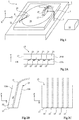
- the figure 1 is a schematic perspective view of a test station adapted to implement a method of adjusting the parallelism of a block of optical fibers with a face of a chip disposed on an XY table.
- the test station 1 comprises, in an orthonormal frame defined by three directions or axes X, Y and Z, a frame 3 on which rests an XY table 5.
- the upper face of the table XY 5 is parallel to the plane defined by the directions X and Y.
- the test station 1 comprises a manipulator arm 7 integral with the frame 3.
- the test station 1 further comprises a sensor 9 integral with the table 5.
- the sensor 9 is moved in the same way, parallel to the plane defined by these directions X and Y.
- the sensor is disposed on a support 10 mounted at the end of an arm 11 fixed to the table 5.
- a control and processing circuit 12 receives the output signal from the sensor 9 and provides control signals to the manipulator arm 7 and to the XY table 5.
- a block 13 of optical fibers 15 is fixed to the manipulator arm 7, usually at a level of end of it.
- the block 13 is arranged so that its lower face 17, at which the ends of the fibers 15 are flush, is turned towards the upper face of the XY table 5.
- a semiconductor chip 19 is disposed on the XY table 5 , the upper face of the chip 19 being parallel to the plane defined by the X and Y directions.
- the manipulator arm 7 is adapted to move the block 13 at least in the direction Z.
- the manipulator arm 7 is also adapted to modify the orientation of the block relative to the XY table 5, by applying rotations to the block 13 at least around two axes different from the axis Z.
- the manipulator arm 7 is for example a six axis manipulator arm whose end bearing the block 13 is movable in translation in the X, Y and Z directions and in rotation about the X axes, Y and Z.
- the movements in translation and in rotation of the manipulator arm 7, and the translational movements of the XY table 5 are carried out by means of displacement devices (not shown), for example step motors or micrometric adjustment screw. These displacement devices are automatically controlled or controlled by the control signals supplied by the processing and control circuit 12.
- FIGS. 2A, 2B and 2C are schematic views respectively from below, from side and from face of the block 13 of fibers 15 of the figure 1 .
- the block 13 consists of two glass plates 13A and 13B glued to each other.
- the plate 13A has grooves 23 at its face glued to the plate 13B, for example V-shaped grooves.
- a fiber 15 In each groove 23 is arranged a fiber 15.
- the block 13 comprises five fibers 15 being understood that, in practice, the block 13 may comprise any number of fibers greater than or equal to two.
- the optical inputs and outputs of an optical integrated circuit to be tested are commonly constituted by coupling networks, each of which is disposed at one end of a waveguide.
- the angle ⁇ between the normal 25 to the lower face 17 of the block 13 and the axis of each fiber 15 is chosen according to the coupling networks used, and is for example between 3 and 15 °, by example 8 °.
- the lower face 17 of the block has, for example, a width of approximately 2 mm for a length of about 4.5 mm.
- FIGS. 3A, 3B, 4A and 4B illustrate successive stages of such a process, the Figures 3A and 3B being side views of the sensor 9 resting on the support 10 and the block 13 of fibers 15 and the Figures 4A and 4B being front views of these same elements.
- the senor 9 is a contact sensor. More particularly, the sensor 9 comprises a Z-shaped deformable element, for example a flexible strip 27, and a device for measuring the Z-shaped deformation of this element, for example a strain gauge, not shown, arranged on the upper or lower face of the element. As a variant, the deformable element made of Z and the device for measuring the Z-shaped deformation correspond to a piezoelectric lamella.
- the sensor further comprises a ball 29 or a point resting on the upper face of the flexible strip 27 and for ensuring a point contact of the sensor 9 with a surface.
- the lamella 27 has a length of between 10 and 20 mm, for example 12 mm, and a width of between 3 and 10 mm, for example 4 mm.
- the ball 29 is for example glass, and has for example a diameter of between 1.5 and 0.5 mm, for example about 1 mm.
- the ball 29 of the sensor 9 is placed opposite a point 31 of the lower face 17 of the block 13 of fibers 15 by moving the table XY 5, thus the sensor 9, in the X and Y directions.
- the block 13 is then moved in Z with the aid of the manipulator arm 7, from a Z reference position to the sensor 9. From the contacting point 31 and the ball 29, the displacement Z causes a deformation of the strip 27 which is detected on the output signal of the sensor 9 by the control circuit and treatment 12 The latter then automatically determines the distance z1 traversed at Z by the block 13 from its reference position until it comes into contact with the sensor 9.
- the block 13 is then returned to its reference position as shown. in figure 3A .
- the ball 29 of the sensor 9 is placed opposite a point 33 of the lower face 17 of the block 13 of fibers 15 by moving the table XY 5 by a distance y1 in the direction Y.
- the distance in Z, z2, between the ball 29 and the point 33 of the block 13 in its reference position is determined by the circuit 12 similarly to the distance z1.
- Block 13 is then returned to its reference position.
- the block 15, the sensor 9 and the support 10 are in the same positions as at the end of the step illustrated in FIG. figure 3B .
- the ball 29 of the sensor 9 is placed opposite a point 35 of the lower face 17 of the block 13 by moving the table 5 by a distance x1 in the direction X.
- the distance in Z, z3, between the ball 29 and the point 35 of the block 13 in its reference position is determined by the circuit similarly to the distances z1 and z2. Block 13 is then returned to its reference position.
- the differences in distance Z between the points 31 and 33 and between the points 33 and 35, with respect to the sensor 9, are evaluated automatically by the control and processing circuit 12 from the distances stored z1, z2 and z3. Knowing these distance differences in Z and the distances x1 and y1, by applying trigonometry formulas, the control and processing circuit 12 automatically determines the orientation of the face 17 of the block 13 with respect to the upper surface of the table. XY 5 or the semiconductor chip 19.
- control and processing circuit 12 calculates the angle ⁇ 1 between the face 17 of the block 13 and the XY table 5 in a plane orthogonal to the XY table 5 comprising the points 31 and 33 ( figure 3B ), and the angle ⁇ 2 between the face 17 of the block 13 and the table XY 5 in a plane orthogonal to the table XY comprising the points 33 and 35 ( Figure 4B ).
- the control and processing circuit 12 automatically determines the control signals to be supplied to the rotational displacement devices of the arm 7 to modify the orientation of the block 13 compared to the XY table and ensure the desired parallelism.
- this corresponds to applying to the block a rotation of angle ⁇ 1 around the axis X and a rotation of angle ⁇ 2 around the axis Y.
- the points 31, 33 and 35 of the lower face 17 of the block 13 are chosen close to corners of this face 17.
- the displacement distances in the X and Y directions are important which limits the influence of a possible absolute displacement error in these directions, and allows a better accuracy of adjustment of the parallelism.
- contact sensors are simple and inexpensive devices and their use is particularly simple and effective. Indeed, as indicated above, they can be used to measure the distance between a reference position of the manipulator arm and a contact position without the need to make an absolute distance measurement.
- the movements Z of the manipulator arm are provided by a stepper motor and it It will suffice, knowing the value of a step, to count the number of steps between the two positions of the manipulator arm.
- the contact sensors make it possible to obtain Z measurement accuracies leading to a parallelism adjustment with the required precision.
- a sensor consisting of a 4 mm x 12 mm blade and a 120 ohm (2.5 mm x 6 mm) strain gauge is used, a measurement accuracy of 5 ⁇ m is obtained. that is to say that the sensor 9 makes it possible to determine the angle ⁇ 1 with an accuracy of 0.06 ° and the angle ⁇ 2 with an accuracy of 0.015 ° when the face 17 has the dimensions indicated in relation to the FIGS. 2A to 2C .
- the contact sensors are not sensitive to the nature of the material or materials of the surface with respect to which the distance is measured.
- the senor 9 described here does not require any calibration phase.
- a contact sensor can be positioned roughly without affecting the Z-axis distance measurement, unlike other sensors such as optical sensors that need to be perfectly aligned on the Z-axis. .
- the electrical consumption of a contact sensor, in particular of the sensor 9 described above, is very low.
- the contact sensor 9 is replaced by another distance sensor Z, for example a optical distance sensor such as a flight time sensor, a capacitive distance sensor, an inductive distance sensor, a magneto-inductive distance sensor, or an eddy current sensor.
- a contact sensor which has the advantages set out above, the other sensors being generally less simple, more expensive and more difficult to use.
- an optical distance sensor of the flight time type requires a source of light emission and a light receiver, and therefore costs much more than a contact sensor.
- the source of light emission and the sensor must be synchronized which makes these sensors flight time complex.
- the orientation of the block 13 with respect to the XY table 5 is modified after each evaluation of a distance difference in Z between two points with respect to the sensor 9.
- the angle ⁇ 1 is calculated on the basis of the distance y1 and the distance difference in Z, z1-z2, between the points 31 and 33, and a rotation of angle ⁇ 1 around the axis X is applied to block 13 to adjust the parallelism.
- the stages of Figures 4A and 4B are performed, a new measurement of the distance z2 being carried out at the step of the Figure 4A .
- the angle ⁇ 2 is then calculated on the basis of the distance x1 and the distance difference in Z, z2-z3, between the points 33 and 35, and a rotation of angle ⁇ 2 around the axis Y is applied to block 13 to correct the parallelism.
- the relationships between the controls applied to the rotational displacement devices of the arm 7 and the angles of the rotations resulting therefrom are not known.
- the method described above can be implemented by successive approximations.
- the block orientation 13 is roughly modified on the basis angles ⁇ 1 and ⁇ 2.
- the stages of Figures 3A to 4B and rough modification of the orientation of the block 13 are then repeated until differences in distance Z and angles ⁇ 1 and ⁇ 2 are zero or almost.
- the block 13 can be moved in X and Y with respect to the XY table 5 and to the sensor 9 rather than the reverse as has been described in connection with the FIGS. 3A, 3B, 4A and 4B .
- the block 13 is moved parallel to the upper surface of the XY table 5
- the distribution of the fibers 15 in the block 13 may be different from that described above.
- the fibers may not be coplanar and / or not be distributed at a given pitch.
- the sensor 9 can be placed at any chosen location as long as it is integral with the movement of the XY table.
- the sensor 9 can be arranged on the XY table 5 or on the semiconductor chip 19.
- measurement points are sufficient to carry out the above method, more than three measurement points can be provided, for example four measurement points each of which can correspond to a corner of the face 17.
- the block of fibers can be replaced by any other element comprising a face that is sought to make parallel to the upper face of the table XY or a device resting on this table.
- the above method can be implemented to parallel a face of an optical prism with the upper surface of a chip resting on the XY table and comprising a source of light emission that is desired to study.
- the above method can be implemented in a conditioning station comprising an XY table and a manipulator arm for producing, when packaging an integrated optical circuit chip, the alignment of a block of fibers with optical inputs / outputs of this chip.
- test steps can be performed, including test steps. Modifications can then be made to the test station 1 described in connection with the figure 1 to implement these steps.
- a Z-distance sensor facing the semiconductor chip 19 can be fixed. at the end of the arm 7 carrying the block 13.
- the distance Z between the semiconductor chip 19 and the lower face 17 of the block 13 is measured after each displacement, and if necessary, corrected by moving the block 13 Z.
Landscapes
- Physics & Mathematics (AREA)
- General Physics & Mathematics (AREA)
- Optics & Photonics (AREA)
- Length Measuring Devices By Optical Means (AREA)
- Container, Conveyance, Adherence, Positioning, Of Wafer (AREA)
- Die Bonding (AREA)
Applications Claiming Priority (1)
| Application Number | Priority Date | Filing Date | Title |
|---|---|---|---|
| FR1751998A FR3063833B1 (fr) | 2017-03-10 | 2017-03-10 | Procede de reglage du parallelisme d'un bloc de fibres avec une surface d'une puce |
Publications (2)
| Publication Number | Publication Date |
|---|---|
| EP3373053A1 true EP3373053A1 (de) | 2018-09-12 |
| EP3373053B1 EP3373053B1 (de) | 2022-02-23 |
Family
ID=59296956
Family Applications (1)
| Application Number | Title | Priority Date | Filing Date |
|---|---|---|---|
| EP18160425.7A Active EP3373053B1 (de) | 2017-03-10 | 2018-03-07 | Regulierungsverfahren der parallelität eines faserblocks mit einer chip-oberfläche |
Country Status (3)
| Country | Link |
|---|---|
| US (1) | US10247890B2 (de) |
| EP (1) | EP3373053B1 (de) |
| FR (1) | FR3063833B1 (de) |
Families Citing this family (2)
| Publication number | Priority date | Publication date | Assignee | Title |
|---|---|---|---|---|
| FR3089344B1 (fr) | 2018-11-30 | 2021-01-22 | Commissariat Energie Atomique | Test de circuit photonique intégré |
| US12496511B2 (en) * | 2023-03-09 | 2025-12-16 | Microsoft Technology Licensing, Llc | Piezoelectric input device |
Citations (7)
| Publication number | Priority date | Publication date | Assignee | Title |
|---|---|---|---|---|
| US6325551B1 (en) * | 1999-12-08 | 2001-12-04 | New Focus, Inc. | Method and apparatus for optically aligning optical fibers with optical devices |
| US20020110335A1 (en) * | 2001-02-14 | 2002-08-15 | Wagner David K. | Packaging and alignment methods for optical components, and optical apparatus employing same |
| US6556751B1 (en) * | 1999-01-19 | 2003-04-29 | Samsung Electronics Co., Ltd. | Apparatus for and method of measuring optical alignment of fiber block |
| US20030113069A1 (en) * | 2001-12-17 | 2003-06-19 | Sang-Ho Kim | Optical fiber alignment system |
| KR20040019516A (ko) * | 2002-08-28 | 2004-03-06 | 삼성전자주식회사 | 거리 센서를 구비한 광축 정렬 장치와 광축 정렬 방법 |
| US20040052470A1 (en) * | 2002-09-18 | 2004-03-18 | Sang-Ho Kim | Alignment apparatus and method for optical fiber blocks |
| US20070175563A1 (en) * | 2006-02-02 | 2007-08-02 | Fujitsu Limited | Optical component manufacturing apparatus and method, and optical component lens assembling apparatus |
Family Cites Families (1)
| Publication number | Priority date | Publication date | Assignee | Title |
|---|---|---|---|---|
| US5511572A (en) | 1994-07-25 | 1996-04-30 | Carter; Mark C. | Collapsible shelter with flexible, collapsible canopy |
-
2017
- 2017-03-10 FR FR1751998A patent/FR3063833B1/fr not_active Expired - Fee Related
-
2018
- 2018-03-07 EP EP18160425.7A patent/EP3373053B1/de active Active
- 2018-03-09 US US15/916,495 patent/US10247890B2/en active Active
Patent Citations (7)
| Publication number | Priority date | Publication date | Assignee | Title |
|---|---|---|---|---|
| US6556751B1 (en) * | 1999-01-19 | 2003-04-29 | Samsung Electronics Co., Ltd. | Apparatus for and method of measuring optical alignment of fiber block |
| US6325551B1 (en) * | 1999-12-08 | 2001-12-04 | New Focus, Inc. | Method and apparatus for optically aligning optical fibers with optical devices |
| US20020110335A1 (en) * | 2001-02-14 | 2002-08-15 | Wagner David K. | Packaging and alignment methods for optical components, and optical apparatus employing same |
| US20030113069A1 (en) * | 2001-12-17 | 2003-06-19 | Sang-Ho Kim | Optical fiber alignment system |
| KR20040019516A (ko) * | 2002-08-28 | 2004-03-06 | 삼성전자주식회사 | 거리 센서를 구비한 광축 정렬 장치와 광축 정렬 방법 |
| US20040052470A1 (en) * | 2002-09-18 | 2004-03-18 | Sang-Ho Kim | Alignment apparatus and method for optical fiber blocks |
| US20070175563A1 (en) * | 2006-02-02 | 2007-08-02 | Fujitsu Limited | Optical component manufacturing apparatus and method, and optical component lens assembling apparatus |
Also Published As
| Publication number | Publication date |
|---|---|
| US20180259727A1 (en) | 2018-09-13 |
| EP3373053B1 (de) | 2022-02-23 |
| US10247890B2 (en) | 2019-04-02 |
| FR3063833A1 (fr) | 2018-09-14 |
| FR3063833B1 (fr) | 2019-03-29 |
Similar Documents
| Publication | Publication Date | Title |
|---|---|---|
| EP1972886B1 (de) | Verfahren und Vorrichtung zur Vermessung einer Objektoberfläche mittels eines Abstandssensors, der den Brennpunkt misst | |
| CH623502A5 (de) | ||
| FR2551860A1 (fr) | Installation pour la determination des coordonnees spatiales d'un point d'une piece, notamment pour le controle d'un outillage tel qu'un outillage de soudage de carrosserie de vehicule automobile | |
| EP3861282B1 (de) | Vorrichtung zur chromatischen konfokalen messung einer lokalen höhen- und/oder orientierung einer probenoberfläche und entsprechende verfahren zur messung der höhe oder rauheit einer probe | |
| EP3373053B1 (de) | Regulierungsverfahren der parallelität eines faserblocks mit einer chip-oberfläche | |
| EP3069185A1 (de) | Dreidimensionale fokussierungsvorrichtung und verfahren für ein mikroskop | |
| FR2895801A1 (fr) | Systeme d'acquisition de donnees sismiques a six composantes | |
| EP0649001B1 (de) | Vorrichtung und Verfahren zum Messen der Form oder/und der Flachheit eines sich bewegenden Materials | |
| US20080100850A1 (en) | Surface height and focus sensor | |
| FR2467385A1 (fr) | Appareil et son utilisation en vue de controler l'alignement d'essieux de roues | |
| CH622204A5 (de) | ||
| WO2020245128A1 (fr) | Système de visée comprenant un dispositif de visée orientable par rapport à une embase, apte à mettre en œuvre un procédé de calibrage sur site simple et rapide | |
| CN100588934C (zh) | 偏芯量测量方法 | |
| EP0842409B1 (de) | Gerät und verfahren zur streifen-ablenkungsmessung | |
| FR3139626A1 (fr) | Dispositif de mesure de front d'onde optique et procédé de mesure associé | |
| BE1012029A3 (fr) | Procede et dispositif de positionnement d'un objet par rapport a une direction de reference. | |
| EP0505233B1 (de) | Einrichtung zum Messen der Winkellage eines schwenkbaren Teils relativ zu einem feststehenden Teil, insbesondere eines Teleskoprahmens relativ zu dessen Halterungsgestell | |
| FR2936614A1 (fr) | Mise au point d'un microscope a reflexion | |
| EP4423455B1 (de) | Deflektometriemessverfahren | |
| FR2584007A1 (fr) | Dispositif a positionnement optique | |
| FR2638115A1 (fr) | Procede de calage d'un bras de robot et robots utilisant ce procede | |
| EP3990856A1 (de) | Maschine und verfahren zur inspektion von mechanischen teilen | |
| FR2739445A1 (fr) | Procede de mesure physique par reflectometrie, et dispositif formant capteur optique associe | |
| FR2506930A1 (fr) | Procede et dispositif d'evaluation de la position d'une fibre optique dans un embout de connecteur et application a son positionnement | |
| EP0316208A1 (de) | Regelsystem der Winkelverstellung einer Drehscheibe und Anwendung in einem X-Strahlspektrometer |
Legal Events
| Date | Code | Title | Description |
|---|---|---|---|
| PUAI | Public reference made under article 153(3) epc to a published international application that has entered the european phase |
Free format text: ORIGINAL CODE: 0009012 |
|
| STAA | Information on the status of an ep patent application or granted ep patent |
Free format text: STATUS: REQUEST FOR EXAMINATION WAS MADE |
|
| 17P | Request for examination filed |
Effective date: 20180307 |
|
| AK | Designated contracting states |
Kind code of ref document: A1 Designated state(s): AL AT BE BG CH CY CZ DE DK EE ES FI FR GB GR HR HU IE IS IT LI LT LU LV MC MK MT NL NO PL PT RO RS SE SI SK SM TR |
|
| AX | Request for extension of the european patent |
Extension state: BA ME |
|
| STAA | Information on the status of an ep patent application or granted ep patent |
Free format text: STATUS: EXAMINATION IS IN PROGRESS |
|
| 17Q | First examination report despatched |
Effective date: 20201029 |
|
| GRAP | Despatch of communication of intention to grant a patent |
Free format text: ORIGINAL CODE: EPIDOSNIGR1 |
|
| STAA | Information on the status of an ep patent application or granted ep patent |
Free format text: STATUS: GRANT OF PATENT IS INTENDED |
|
| RIC1 | Information provided on ipc code assigned before grant |
Ipc: G01B 21/16 20060101ALN20211115BHEP Ipc: G01D 5/04 20060101ALN20211115BHEP Ipc: G01B 7/00 20060101ALN20211115BHEP Ipc: G02B 6/42 20060101ALI20211115BHEP Ipc: G01L 1/04 20060101ALI20211115BHEP Ipc: G01M 11/00 20060101ALI20211115BHEP Ipc: G02B 6/38 20060101AFI20211115BHEP |
|
| INTG | Intention to grant announced |
Effective date: 20211217 |
|
| GRAS | Grant fee paid |
Free format text: ORIGINAL CODE: EPIDOSNIGR3 |
|
| GRAA | (expected) grant |
Free format text: ORIGINAL CODE: 0009210 |
|
| STAA | Information on the status of an ep patent application or granted ep patent |
Free format text: STATUS: THE PATENT HAS BEEN GRANTED |
|
| AK | Designated contracting states |
Kind code of ref document: B1 Designated state(s): AL AT BE BG CH CY CZ DE DK EE ES FI FR GB GR HR HU IE IS IT LI LT LU LV MC MK MT NL NO PL PT RO RS SE SI SK SM TR |
|
| REG | Reference to a national code |
Ref country code: GB Ref legal event code: FG4D Free format text: NOT ENGLISH |
|
| REG | Reference to a national code |
Ref country code: CH Ref legal event code: EP |
|
| REG | Reference to a national code |
Ref country code: DE Ref legal event code: R096 Ref document number: 602018031096 Country of ref document: DE |
|
| REG | Reference to a national code |
Ref country code: AT Ref legal event code: REF Ref document number: 1470895 Country of ref document: AT Kind code of ref document: T Effective date: 20220315 |
|
| REG | Reference to a national code |
Ref country code: IE Ref legal event code: FG4D Free format text: LANGUAGE OF EP DOCUMENT: FRENCH |
|
| REG | Reference to a national code |
Ref country code: LT Ref legal event code: MG9D |
|
| REG | Reference to a national code |
Ref country code: NL Ref legal event code: MP Effective date: 20220223 |
|
| REG | Reference to a national code |
Ref country code: AT Ref legal event code: MK05 Ref document number: 1470895 Country of ref document: AT Kind code of ref document: T Effective date: 20220223 |
|
| PG25 | Lapsed in a contracting state [announced via postgrant information from national office to epo] |
Ref country code: SE Free format text: LAPSE BECAUSE OF FAILURE TO SUBMIT A TRANSLATION OF THE DESCRIPTION OR TO PAY THE FEE WITHIN THE PRESCRIBED TIME-LIMIT Effective date: 20220223 Ref country code: RS Free format text: LAPSE BECAUSE OF FAILURE TO SUBMIT A TRANSLATION OF THE DESCRIPTION OR TO PAY THE FEE WITHIN THE PRESCRIBED TIME-LIMIT Effective date: 20220223 Ref country code: PT Free format text: LAPSE BECAUSE OF FAILURE TO SUBMIT A TRANSLATION OF THE DESCRIPTION OR TO PAY THE FEE WITHIN THE PRESCRIBED TIME-LIMIT Effective date: 20220623 Ref country code: NO Free format text: LAPSE BECAUSE OF FAILURE TO SUBMIT A TRANSLATION OF THE DESCRIPTION OR TO PAY THE FEE WITHIN THE PRESCRIBED TIME-LIMIT Effective date: 20220523 Ref country code: NL Free format text: LAPSE BECAUSE OF FAILURE TO SUBMIT A TRANSLATION OF THE DESCRIPTION OR TO PAY THE FEE WITHIN THE PRESCRIBED TIME-LIMIT Effective date: 20220223 Ref country code: LT Free format text: LAPSE BECAUSE OF FAILURE TO SUBMIT A TRANSLATION OF THE DESCRIPTION OR TO PAY THE FEE WITHIN THE PRESCRIBED TIME-LIMIT Effective date: 20220223 Ref country code: HR Free format text: LAPSE BECAUSE OF FAILURE TO SUBMIT A TRANSLATION OF THE DESCRIPTION OR TO PAY THE FEE WITHIN THE PRESCRIBED TIME-LIMIT Effective date: 20220223 Ref country code: ES Free format text: LAPSE BECAUSE OF FAILURE TO SUBMIT A TRANSLATION OF THE DESCRIPTION OR TO PAY THE FEE WITHIN THE PRESCRIBED TIME-LIMIT Effective date: 20220223 Ref country code: BG Free format text: LAPSE BECAUSE OF FAILURE TO SUBMIT A TRANSLATION OF THE DESCRIPTION OR TO PAY THE FEE WITHIN THE PRESCRIBED TIME-LIMIT Effective date: 20220523 |
|
| PG25 | Lapsed in a contracting state [announced via postgrant information from national office to epo] |
Ref country code: PL Free format text: LAPSE BECAUSE OF FAILURE TO SUBMIT A TRANSLATION OF THE DESCRIPTION OR TO PAY THE FEE WITHIN THE PRESCRIBED TIME-LIMIT Effective date: 20220223 Ref country code: LV Free format text: LAPSE BECAUSE OF FAILURE TO SUBMIT A TRANSLATION OF THE DESCRIPTION OR TO PAY THE FEE WITHIN THE PRESCRIBED TIME-LIMIT Effective date: 20220223 Ref country code: GR Free format text: LAPSE BECAUSE OF FAILURE TO SUBMIT A TRANSLATION OF THE DESCRIPTION OR TO PAY THE FEE WITHIN THE PRESCRIBED TIME-LIMIT Effective date: 20220524 Ref country code: FI Free format text: LAPSE BECAUSE OF FAILURE TO SUBMIT A TRANSLATION OF THE DESCRIPTION OR TO PAY THE FEE WITHIN THE PRESCRIBED TIME-LIMIT Effective date: 20220223 Ref country code: AT Free format text: LAPSE BECAUSE OF FAILURE TO SUBMIT A TRANSLATION OF THE DESCRIPTION OR TO PAY THE FEE WITHIN THE PRESCRIBED TIME-LIMIT Effective date: 20220223 |
|
| PG25 | Lapsed in a contracting state [announced via postgrant information from national office to epo] |
Ref country code: IS Free format text: LAPSE BECAUSE OF FAILURE TO SUBMIT A TRANSLATION OF THE DESCRIPTION OR TO PAY THE FEE WITHIN THE PRESCRIBED TIME-LIMIT Effective date: 20220623 |
|
| PG25 | Lapsed in a contracting state [announced via postgrant information from national office to epo] |
Ref country code: SM Free format text: LAPSE BECAUSE OF FAILURE TO SUBMIT A TRANSLATION OF THE DESCRIPTION OR TO PAY THE FEE WITHIN THE PRESCRIBED TIME-LIMIT Effective date: 20220223 Ref country code: SK Free format text: LAPSE BECAUSE OF FAILURE TO SUBMIT A TRANSLATION OF THE DESCRIPTION OR TO PAY THE FEE WITHIN THE PRESCRIBED TIME-LIMIT Effective date: 20220223 Ref country code: RO Free format text: LAPSE BECAUSE OF FAILURE TO SUBMIT A TRANSLATION OF THE DESCRIPTION OR TO PAY THE FEE WITHIN THE PRESCRIBED TIME-LIMIT Effective date: 20220223 Ref country code: EE Free format text: LAPSE BECAUSE OF FAILURE TO SUBMIT A TRANSLATION OF THE DESCRIPTION OR TO PAY THE FEE WITHIN THE PRESCRIBED TIME-LIMIT Effective date: 20220223 Ref country code: DK Free format text: LAPSE BECAUSE OF FAILURE TO SUBMIT A TRANSLATION OF THE DESCRIPTION OR TO PAY THE FEE WITHIN THE PRESCRIBED TIME-LIMIT Effective date: 20220223 Ref country code: CZ Free format text: LAPSE BECAUSE OF FAILURE TO SUBMIT A TRANSLATION OF THE DESCRIPTION OR TO PAY THE FEE WITHIN THE PRESCRIBED TIME-LIMIT Effective date: 20220223 |
|
| REG | Reference to a national code |
Ref country code: CH Ref legal event code: PL |
|
| REG | Reference to a national code |
Ref country code: DE Ref legal event code: R097 Ref document number: 602018031096 Country of ref document: DE |
|
| PG25 | Lapsed in a contracting state [announced via postgrant information from national office to epo] |
Ref country code: MC Free format text: LAPSE BECAUSE OF FAILURE TO SUBMIT A TRANSLATION OF THE DESCRIPTION OR TO PAY THE FEE WITHIN THE PRESCRIBED TIME-LIMIT Effective date: 20220223 Ref country code: AL Free format text: LAPSE BECAUSE OF FAILURE TO SUBMIT A TRANSLATION OF THE DESCRIPTION OR TO PAY THE FEE WITHIN THE PRESCRIBED TIME-LIMIT Effective date: 20220223 |
|
| REG | Reference to a national code |
Ref country code: BE Ref legal event code: MM Effective date: 20220331 |
|
| PLBE | No opposition filed within time limit |
Free format text: ORIGINAL CODE: 0009261 |
|
| STAA | Information on the status of an ep patent application or granted ep patent |
Free format text: STATUS: NO OPPOSITION FILED WITHIN TIME LIMIT |
|
| PG25 | Lapsed in a contracting state [announced via postgrant information from national office to epo] |
Ref country code: LU Free format text: LAPSE BECAUSE OF NON-PAYMENT OF DUE FEES Effective date: 20220307 Ref country code: LI Free format text: LAPSE BECAUSE OF NON-PAYMENT OF DUE FEES Effective date: 20220331 Ref country code: IE Free format text: LAPSE BECAUSE OF NON-PAYMENT OF DUE FEES Effective date: 20220307 Ref country code: CH Free format text: LAPSE BECAUSE OF NON-PAYMENT OF DUE FEES Effective date: 20220331 |
|
| 26N | No opposition filed |
Effective date: 20221124 |
|
| PG25 | Lapsed in a contracting state [announced via postgrant information from national office to epo] |
Ref country code: SI Free format text: LAPSE BECAUSE OF FAILURE TO SUBMIT A TRANSLATION OF THE DESCRIPTION OR TO PAY THE FEE WITHIN THE PRESCRIBED TIME-LIMIT Effective date: 20220223 Ref country code: BE Free format text: LAPSE BECAUSE OF NON-PAYMENT OF DUE FEES Effective date: 20220331 |
|
| PG25 | Lapsed in a contracting state [announced via postgrant information from national office to epo] |
Ref country code: IT Free format text: LAPSE BECAUSE OF FAILURE TO SUBMIT A TRANSLATION OF THE DESCRIPTION OR TO PAY THE FEE WITHIN THE PRESCRIBED TIME-LIMIT Effective date: 20220223 |
|
| PG25 | Lapsed in a contracting state [announced via postgrant information from national office to epo] |
Ref country code: HU Free format text: LAPSE BECAUSE OF FAILURE TO SUBMIT A TRANSLATION OF THE DESCRIPTION OR TO PAY THE FEE WITHIN THE PRESCRIBED TIME-LIMIT; INVALID AB INITIO Effective date: 20180307 |
|
| PG25 | Lapsed in a contracting state [announced via postgrant information from national office to epo] |
Ref country code: MK Free format text: LAPSE BECAUSE OF FAILURE TO SUBMIT A TRANSLATION OF THE DESCRIPTION OR TO PAY THE FEE WITHIN THE PRESCRIBED TIME-LIMIT Effective date: 20220223 Ref country code: CY Free format text: LAPSE BECAUSE OF FAILURE TO SUBMIT A TRANSLATION OF THE DESCRIPTION OR TO PAY THE FEE WITHIN THE PRESCRIBED TIME-LIMIT Effective date: 20220223 |
|
| PG25 | Lapsed in a contracting state [announced via postgrant information from national office to epo] |
Ref country code: MT Free format text: LAPSE BECAUSE OF FAILURE TO SUBMIT A TRANSLATION OF THE DESCRIPTION OR TO PAY THE FEE WITHIN THE PRESCRIBED TIME-LIMIT Effective date: 20220223 |
|
| PG25 | Lapsed in a contracting state [announced via postgrant information from national office to epo] |
Ref country code: TR Free format text: LAPSE BECAUSE OF FAILURE TO SUBMIT A TRANSLATION OF THE DESCRIPTION OR TO PAY THE FEE WITHIN THE PRESCRIBED TIME-LIMIT Effective date: 20220223 |
|
| PGFP | Annual fee paid to national office [announced via postgrant information from national office to epo] |
Ref country code: GB Payment date: 20260324 Year of fee payment: 9 |
|
| PGFP | Annual fee paid to national office [announced via postgrant information from national office to epo] |
Ref country code: DE Payment date: 20260320 Year of fee payment: 9 |
|
| PGFP | Annual fee paid to national office [announced via postgrant information from national office to epo] |
Ref country code: FR Payment date: 20260324 Year of fee payment: 9 |