EP3367429A1 - A method for defining patterns for conductive paths in a dielectric layer - Google Patents
A method for defining patterns for conductive paths in a dielectric layer Download PDFInfo
- Publication number
- EP3367429A1 EP3367429A1 EP17158037.6A EP17158037A EP3367429A1 EP 3367429 A1 EP3367429 A1 EP 3367429A1 EP 17158037 A EP17158037 A EP 17158037A EP 3367429 A1 EP3367429 A1 EP 3367429A1
- Authority
- EP
- European Patent Office
- Prior art keywords
- layer
- mask
- trenches
- mandrels
- metal oxide
- Prior art date
- Legal status (The legal status is an assumption and is not a legal conclusion. Google has not performed a legal analysis and makes no representation as to the accuracy of the status listed.)
- Withdrawn
Links
Images




Classifications
-
- H—ELECTRICITY
- H10—SEMICONDUCTOR DEVICES; ELECTRIC SOLID-STATE DEVICES NOT OTHERWISE PROVIDED FOR
- H10W—GENERIC PACKAGES, INTERCONNECTIONS, CONNECTORS OR OTHER CONSTRUCTIONAL DETAILS OF DEVICES COVERED BY CLASS H10
- H10W20/00—Interconnections in chips, wafers or substrates
- H10W20/01—Manufacture or treatment
- H10W20/071—Manufacture or treatment of dielectric parts thereof
- H10W20/081—Manufacture or treatment of dielectric parts thereof by forming openings in the dielectric parts
-
- H—ELECTRICITY
- H10—SEMICONDUCTOR DEVICES; ELECTRIC SOLID-STATE DEVICES NOT OTHERWISE PROVIDED FOR
- H10P—GENERIC PROCESSES OR APPARATUS FOR THE MANUFACTURE OR TREATMENT OF DEVICES COVERED BY CLASS H10
- H10P50/00—Etching of wafers, substrates or parts of devices
- H10P50/73—Etching of wafers, substrates or parts of devices using masks for insulating materials
-
- H—ELECTRICITY
- H10—SEMICONDUCTOR DEVICES; ELECTRIC SOLID-STATE DEVICES NOT OTHERWISE PROVIDED FOR
- H10P—GENERIC PROCESSES OR APPARATUS FOR THE MANUFACTURE OR TREATMENT OF DEVICES COVERED BY CLASS H10
- H10P76/00—Manufacture or treatment of masks on semiconductor bodies, e.g. by lithography or photolithography
- H10P76/40—Manufacture or treatment of masks on semiconductor bodies, e.g. by lithography or photolithography of masks comprising inorganic materials
- H10P76/408—Manufacture or treatment of masks on semiconductor bodies, e.g. by lithography or photolithography of masks comprising inorganic materials characterised by their sizes, orientations, dispositions, behaviours or shapes
- H10P76/4085—Manufacture or treatment of masks on semiconductor bodies, e.g. by lithography or photolithography of masks comprising inorganic materials characterised by their sizes, orientations, dispositions, behaviours or shapes characterised by the processes involved to create the masks
-
- H—ELECTRICITY
- H10—SEMICONDUCTOR DEVICES; ELECTRIC SOLID-STATE DEVICES NOT OTHERWISE PROVIDED FOR
- H10W—GENERIC PACKAGES, INTERCONNECTIONS, CONNECTORS OR OTHER CONSTRUCTIONAL DETAILS OF DEVICES COVERED BY CLASS H10
- H10W20/00—Interconnections in chips, wafers or substrates
- H10W20/01—Manufacture or treatment
- H10W20/031—Manufacture or treatment of conductive parts of the interconnections
- H10W20/056—Manufacture or treatment of conductive parts of the interconnections by filling conductive material into holes, grooves or trenches
-
- H—ELECTRICITY
- H10—SEMICONDUCTOR DEVICES; ELECTRIC SOLID-STATE DEVICES NOT OTHERWISE PROVIDED FOR
- H10W—GENERIC PACKAGES, INTERCONNECTIONS, CONNECTORS OR OTHER CONSTRUCTIONAL DETAILS OF DEVICES COVERED BY CLASS H10
- H10W20/00—Interconnections in chips, wafers or substrates
- H10W20/01—Manufacture or treatment
- H10W20/071—Manufacture or treatment of dielectric parts thereof
- H10W20/081—Manufacture or treatment of dielectric parts thereof by forming openings in the dielectric parts
- H10W20/084—Manufacture or treatment of dielectric parts thereof by forming openings in the dielectric parts for dual-damascene structures
-
- H—ELECTRICITY
- H10—SEMICONDUCTOR DEVICES; ELECTRIC SOLID-STATE DEVICES NOT OTHERWISE PROVIDED FOR
- H10W—GENERIC PACKAGES, INTERCONNECTIONS, CONNECTORS OR OTHER CONSTRUCTIONAL DETAILS OF DEVICES COVERED BY CLASS H10
- H10W20/00—Interconnections in chips, wafers or substrates
- H10W20/01—Manufacture or treatment
- H10W20/071—Manufacture or treatment of dielectric parts thereof
- H10W20/081—Manufacture or treatment of dielectric parts thereof by forming openings in the dielectric parts
- H10W20/089—Manufacture or treatment of dielectric parts thereof by forming openings in the dielectric parts using processes for implementing desired shapes or dispositions of the openings, e.g. double patterning
-
- H—ELECTRICITY
- H10—SEMICONDUCTOR DEVICES; ELECTRIC SOLID-STATE DEVICES NOT OTHERWISE PROVIDED FOR
- H10W—GENERIC PACKAGES, INTERCONNECTIONS, CONNECTORS OR OTHER CONSTRUCTIONAL DETAILS OF DEVICES COVERED BY CLASS H10
- H10W20/00—Interconnections in chips, wafers or substrates
- H10W20/01—Manufacture or treatment
- H10W20/071—Manufacture or treatment of dielectric parts thereof
- H10W20/092—Manufacture or treatment of dielectric parts thereof by smoothing the dielectric parts
-
- H—ELECTRICITY
- H10—SEMICONDUCTOR DEVICES; ELECTRIC SOLID-STATE DEVICES NOT OTHERWISE PROVIDED FOR
- H10P—GENERIC PROCESSES OR APPARATUS FOR THE MANUFACTURE OR TREATMENT OF DEVICES COVERED BY CLASS H10
- H10P14/00—Formation of materials, e.g. in the shape of layers or pillars
- H10P14/60—Formation of materials, e.g. in the shape of layers or pillars of insulating materials
- H10P14/63—Formation of materials, e.g. in the shape of layers or pillars of insulating materials characterised by the formation processes
- H10P14/6326—Deposition processes
- H10P14/6328—Deposition from the gas or vapour phase
- H10P14/6334—Deposition from the gas or vapour phase using decomposition or reaction of gaseous or vapour phase compounds, i.e. chemical vapour deposition
- H10P14/6339—Deposition from the gas or vapour phase using decomposition or reaction of gaseous or vapour phase compounds, i.e. chemical vapour deposition deposition by cyclic CVD, e.g. ALD, ALE or pulsed CVD
-
- H—ELECTRICITY
- H10—SEMICONDUCTOR DEVICES; ELECTRIC SOLID-STATE DEVICES NOT OTHERWISE PROVIDED FOR
- H10P—GENERIC PROCESSES OR APPARATUS FOR THE MANUFACTURE OR TREATMENT OF DEVICES COVERED BY CLASS H10
- H10P14/00—Formation of materials, e.g. in the shape of layers or pillars
- H10P14/60—Formation of materials, e.g. in the shape of layers or pillars of insulating materials
- H10P14/69—Inorganic materials
- H10P14/692—Inorganic materials composed of oxides, glassy oxides or oxide-based glasses
- H10P14/6921—Inorganic materials composed of oxides, glassy oxides or oxide-based glasses containing silicon
- H10P14/69215—Inorganic materials composed of oxides, glassy oxides or oxide-based glasses containing silicon the material being a silicon oxide, e.g. SiO2
-
- H—ELECTRICITY
- H10—SEMICONDUCTOR DEVICES; ELECTRIC SOLID-STATE DEVICES NOT OTHERWISE PROVIDED FOR
- H10P—GENERIC PROCESSES OR APPARATUS FOR THE MANUFACTURE OR TREATMENT OF DEVICES COVERED BY CLASS H10
- H10P14/00—Formation of materials, e.g. in the shape of layers or pillars
- H10P14/60—Formation of materials, e.g. in the shape of layers or pillars of insulating materials
- H10P14/69—Inorganic materials
- H10P14/694—Inorganic materials composed of nitrides
- H10P14/6943—Inorganic materials composed of nitrides containing silicon
- H10P14/69433—Inorganic materials composed of nitrides containing silicon the material being a silicon nitride not containing oxygen, e.g. SixNy or SixByNz
Definitions
- the present inventive concept relates to a method for defining patterns for conductive paths in a dielectric layer.
- An interconnection structure may include one or more metallization levels or tiers, which are formed above the substrate and the semiconductor devices.
- a metallization level includes conductive paths or lines arranged in a dielectric material layer. The dielectric material layer of a metallization level may isolate the conductive paths of the metallization level from a higher and/or a lower metallization level. Conductive paths of different metallization levels may be interconnected by conductive vias extending through the dielectric layers.
- a metallization level may be formed by forming patterns including trenches and holes in a dielectric layer, and filling the trenches and holes with a conductive material. Such a process may be referred to as a dual damascene process. The process may be repeated to form a stack of metallization levels on top of each other.
- Patterns may be formed in a mask layer arranged above the dielectric layer using lithographic techniques and etching. Multiple patterning techniques like (litho-etch) x , or pitch splitting techniques such as self-aligned double patterning (SADP) or quadruple patterning (SAQP), may be used to enable patterns with sub-lithographic critical dimensions. Multiple patterning may be combined with block techniques to enable forming of interrupted or discontinuous lines.
- An objective of the present inventive concept is to provide an improved method for defining patterns for conductive paths in a dielectric layer. Further and alternative objectives may be understood from the following.
- a method for defining patterns for conductive paths in a dielectric layer comprising:
- the inventive method enables definition, in a mask layer, of patterns for conductive paths or conductive lines in a dielectric layer of a metallization level.
- the patterns may be formed as trenches in the mask layer and subsequently transferred into the dielectric layer.
- the position and dimension of the trenches may be established by the set of mandrels having side wall spacers.
- Mandrels having pairs of side wall spacers may be formed by techniques (such as multi patterning techniques) enabling sub-lithographic feature sizes.
- the metal oxide planarization layer includes TiOx, ZrOx or HfOx.
- the set of mandrels may advantageously be formed by oxyphous silicon (a-Si), advantageously strained a-Si.
- the set of mandrels may alternatively be formed by SiN.
- the side wall spacers may advantageously be formed by a silicon oxide, for instance SiO 2 . Other combinations of materials are however also possible.
- the set of mandrels may be formed by a first material
- the side wall spacers may be formed by a second material
- the mask layer may be formed by a third material, wherein the first, the second and the third material are different materials.
- the first material may be etched selectively from the second material.
- the third material may be etched selectively from the first and the second material.
- the first material may be etched selectively from the metal oxide planarization layer.
- the metal oxide planarization layer may be etched selectively from the second material.
- the metal oxide planarization layer may be etched selectively from the third material.
- a material "A" which may be etched selectively from a material “B” means that material A may be etched at a substantially greater rate than material B, in a given etch process.
- a feature of material A arranged adjacent to a feature of material B may be removed in an etch process without appreciably affecting the feature of material B.
- first feature such as a layer, a level or other structure
- second feature such as a layer, a level or other structure
- first feature is formed above the second feature (as seen) in a normal direction to the main surface or in-plane extension of the feature, e.g. layer or level, or equivalently in the normal direction to a substrate on which the metallization level is to be formed.
- first feature such as a layer, a level or other structure
- second feature such as a layer, a level or other structure
- first feature is formed directly on the second feature, i.e. in abutment with the second feature, or with one or more layers intermediate the first and the second feature, i.e. not in direct contact with the second feature.
- metalization level is hereby meant a structure including conductive paths arranged in a dielectric material layer.
- the method may be repeatedly performed for definition, in a mask layer, of patterns for conductive paths or conductive lines in a dielectric layer of two or more metallization levels of a stack of metallization levels.
- a trench in a layer is hereby meant a recess in the layer.
- a trench may, at least along a portion thereof, extend in a straight line and present a uniform width.
- the mask layer formed above the dielectric layer may be any layer or layer stack having the ability to withstand, and accordingly remain following, the removal of the metal oxide planarization layer.
- the mask layer may for instance be a non-resist based mask layer.
- the mask layer may advantageously be a "hard” mask layer.
- the mask layer may advantageously be formed by TiN.
- the mask layer may be formed on the dielectric layer.
- the hard mask layer may be formed directly on the dielectric layer or with one or more intermediate layers between the dielectric layer and the hard mask layer.
- the set of mandrels which also may be referred to as a set of cores, may be formed by a set of parallel mandrel lines.
- the set of mandrels with side wall spacers may be formed using a multiple patterning process such as SADP or SAQP.
- the set of mandrels with side wall spacers may be formed directly on the mask layer or with one or more intermediate layers between the mask layer and the set of mandrels.
- An intermediate buffer layer for instance of SiN, may be formed between the mask layer and the set of mandrels for facilitating forming of the set of mandrels.
- a remaining mask layer portion may hence be formed at positions between side wall spacers of adjacent pairs of mandrels of said at least a subset of the set of mandrels.
- said at least a subset of said first set of trenches may be formed as a set of discontinuous or interrupted trenches, each trench with a first and a second trench portion on opposite sides of a remaining portion of the mask layer.
- Conductive lines with a tip-to-tip configuration may thereby be formed in the dielectric layer.
- the block mask By forming the block mask prior to removing the set of mandrels, the block mask (due to the presence of the mandrels) may be allowed to extend farther than merely across the distance separating side wall spacers of adjacent pairs of mandrels. Especially, an overlap between the block mask and a given mandrel (which mandrel defines a position of one of the second set of trenches to be formed) will not result in formation of a non-intended remaining block portion in said one trench of the second set of trenches. The dimensional and alignment requirements for the block mask may thereby be relaxed.
- the method may further comprise removing the block mask prior to covering the set of mandrels with the metal oxide planarization layer.
- a remaining mask layer portion may hence be formed at positions between side wall spacers on opposite sides of each trench of said at least a subset of trenches in the metal oxide planarization layer.
- said at least a subset of said second set of trenches may be formed as a set of discontinuous or interrupted trenches, each with a first and a second trench portion on opposite sides of a remaining portion of the mask layer.
- Conductive lines with a tip-to-tip configuration may thereby be formed in the dielectric layer.
- the block mask By forming the block mask prior to removing the metal oxide planarization layer, the block mask (due to the presence of the metal oxide planarization layer in the first set of trenches) may be allowed to extend farther than merely across the width of a pair of side wall spacers. The dimensional and alignment requirements for the block mask may thereby be relaxed.
- This embodiment may advantageously be combined with the aforementioned embodiment including forming of the first block mask.
- the first block mask and the second block mask may be formed at different longitudinal positions along the mandrels / trenches in the metallization level.
- the method may further comprise removing the (second) block mask subsequent to said transfer of the trenches into the mask layer.
- the method further comprises: removing the metal oxide planarization layer, wherein the first set of trenches are exposed, and transferring the first and second sets of trenches into the dielectric layer by etching the dielectric layer through said first and second sets of trenches.
- the first and second trenches may be transferred into the dielectric layer.
- the remaining portions of the mask layer may act as an etch mask, counteracting etching of regions of the dielectric layer covered by the remaining portions of the mask layer.
- the method may further comprise filling the trenches in the dielectric layer with a conductive material.
- the trenches may be at least partially filled with a conductive material.
- the conductive material may be a single metal or a mixture or alloy of a metal and another material.
- a complete filling of the trenches is advantageous since it allows the entire cross-sectional area, allowed by the trenches in the dielectric layer, to be filled by the conductive material to obtain a low-resistance interconnect structure.
- the act of filing with a conductive material may comprise forming the conductive material also above the dielectric layer and removing the conductive material in locations outside of the trenches of the dielectric layer and the deepened first and second holes. The removing of excess conductive material may divide the deposited conductor into separate paths extending within the trenches of the dielectric layer.
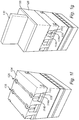
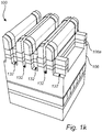
- Figs 1a-k schematically illustrates a method for defining patterns for conductive paths in a dielectric layer.
- Fig. 1 a shows, in perspective, a section of a semiconductor structure or intermediate device 100.
- the structure 100 may extend laterally or horizontally beyond the illustrated section.
- the illustrated planes of section extending through the structure 100 are common to all the figures.
- the structure 100 includes in a bottom-up direction a semiconductor substrate 102.
- An active device layer 103 including semiconductor devices such as transistors are fabricated on a main surface of the substrate 102.
- the active device layer 103 may also be referred to as a front-end-of-line portion (FEOL-portion 103).
- a first metallization level 104 including conductive lines arranged in a dielectric layer, is formed above the FEOL-portion 103.
- a base layer 105 is formed on the first metallization level 104.
- the base layer 105 may include a SiCN layer.
- the structure 100 includes a dielectric layer 106.
- the dielectric layer 106 forms a dielectric layer of the metallization level which is to be formed.
- the dielectric layer 106 may include a silicon oxide layer, for instance SiO 2 , or another low-K dielectric material.
- the dielectric layer 106 may include a stack of layers of different dielectric materials, such as an interface layer and/or an oxide capping layer.
- a mask layer 108 is formed on the dielectric layer 106.
- the mask layer 108 covers an upper surface of the dielectric layer 106.
- the mask layer 108 may form a hard mask layer.
- the mask layer 108 may be formed by a TiN-layer.
- the mask layer 108 may be formed by atomic layer deposition (ALD).
- a set of mandrels 112 are formed on the mask layer 108.
- Fig. 1 a shows three mandrels, however this is merely an illustrational example and typically a greater number of mandrels may be formed above the mask layer 108.
- the set of mandrels 112 form elongated structures, or lines, extending in parallel to each other.
- Each mandrel 112 is provided with a respective pair of side wall spacers 114a, 114b.
- Each pair of side wall spacers 114a, 114b is formed by a first side wall spacer 114a, formed on a first side wall surface of a mandrel 112, and a second side wall spacer 114b, formed on a second side wall surface of said mandrel 112.
- the first and second side wall surfaces are opposite side wall surfaces of said mandrel 112.
- the gap or space between a first side wall spacer 114a on a first mandrel 112 and a second side wall spacer 114b on a second mandrel 112, next or adjacent to the first mandrel, defines the position of a trench of a first set of trenches which are to be formed in the mask layer 108.
- the positions of the mandrels 112 define the positions of a second set of trenches which are to be formed in the mask layer 108.
- the mandrels 112 with the side wall spacers 114a, 114b may be formed using multiple patterning techniques:
- a resist-based mask layer (not shown in Fig. 1 a) may be deposited on the mandrel layer.
- the resist-based mask layer may be deposited in a spin-coating process.
- a pattern for defining the mandrels 112 may be formed in the resist-based mask layer using single- or multiple exposure lithography.
- the pattern of the resist-based mask layer may be transferred into the mandrel layer by etching, thereby forming the mandrels 112.
- the mandrels 112 may thereafter be covered by a conformal spacer material layer.
- the spacer material layer may for instance be a silicon oxide, for instance SiO 2 .
- the spacer material layer may be deposited in an ALD process. Physically separated side wall spacers 114a, 114b may be formed by anisotropically etching the spacer material layer such that the spacer material layer remains only on the sidewalls of the mandrels 112.
- two mandrel layers may be used, a top and a bottom mandrel layer.
- a first set of mandrels may be formed in the top mandrel layer in similar manner as in the SADP-process.
- a first set of side wall spacers may be formed on the first set of mandrels in similar manner as in the SADP-process. The first set of mandrels may thereafter be removed selectively from the first set of side wall spacers by etching.
- the bottom mandrel layer may thereafter be etched using the first set of spacers as an etch mask, wherein the pattern defined by the first set of spacers may be transferred to the bottom mandrel layer, thereby forming the set of mandrels 112 shown in Fig. 1a .
- the side wall spacers 114a, 114b may thereafter be formed in a corresponding manner as the first set of side wall spacers, following removal of remaining portions of the top mandrel layer.
- the first set of mandrels may in principle also be produced by a line doubling process such as the above-described SAQP-process. Although there is in principle no limit in the number of line doubling process that can be used, each doubling process however becomes more technically challenging. Hence, in practice a limit, dependent inter alia on accuracy of equipment and control of process conditions, does exist.
- the structure 100 may, as shown, include a buffer layer 110 forming an intermediate layer between the buffer layer 108 and the mandrel layer.
- a SiN buffer layer may facilitate deposition of an a-Si mandrel layer.
- a SiO 2 buffer layer may facilitate deposition of a SiN mandrel layer.
- a block mask layer 116 has been formed to cover the set of mandrels 112 and the side wall spacers 114a, 114b.
- the block mask layer 116 fills the gaps or spaces between side wall spacers 114a, 114b of adjacent mandrels 112.
- the block mask layer 116 may include an organic spin-on layer.
- the block mask layer 116 may be formed by a spin-on-carbon (SOC) layer.
- a patterned resist-based mask layer 120 is formed on the block mask layer 116.
- the mask layer 120 is patterned to include at least one elongated mask portion, extending in a direction transverse to the longitudinal direction of the mandrels 112.
- an intermediate layer 118 may be arranged between the block mask layer 116 and the mask layer 120.
- the intermediate layer 118 may include a spin-on-glass layer (SOG), a thin layer of SiO 2 , a-Si, SiON or SiOC.
- SOG spin-on-glass layer
- An intermediate layer 118 may be used for improving the fidelity of a transfer of the pattern of the patterned resist-based mask layer 120 into the block mask layer 116.
- the pattern defined by the patterned resist-based mask layer 120 has been transferred into the block mask layer 116 by etching while using the mask layer 120 as an etch mask.
- the mask layer 120 may thereafter be stripped, optionally along with the intermediate layer 118, if present.
- a first block mask 116' has been formed by the portions of the block mask layer 116 previously covered by the patterned resist-based mask layer 120. Accordingly, the first block mask 116' includes at least one elongated mask portion, extending in a direction transverse to the longitudinal direction of the mandrels 112.
- the pattern formed by the block mask 116', and the exposed portions of the mandrels 112 and the side wall spacers 114a, 114b is transferred into the mask layer 108 (and into the buffer layer 110 if present).
- the pattern transfer may be performed by etching the mask layer 108 (and the buffer layer 110) using the block mask 116' and the mandrels 112 and the side wall spacers 114a, 114b as a combined etch mask.
- a mask layer 108 of TiN may be etched selectively from mandrels 112 of a-Si or SiN, side wall spacers 114a, 114b of SiO 2 and a block mask 116' of an organic spin-on material, using a dry etch process.
- trenches 122 which may be commonly referred to as a first set of trenches 122, extending between side wall spacers 114a, 114b of adjacent mandrels 112, is thereby formed in the mask layer 108.
- Each trench 122 in the mask layer 108 is formed at a position, in the mask layer 108, below the gaps between side wall spacers 114a, 114b on adjacent mandrels 112.
- the trenches 122 extend in parallel to each other.
- a bottom surface of each trench 122 is formed by the upper surface of the dielectric layer 106.
- the trenches 122 are interrupted by remaining portions 108a of the mask layer 108.
- the remaining portions 108a may be referred to as first block portions 108a of the mask layer 108.
- the block portions 108a is a consequence of the presence of the block mask 116' during the pattern transfer into the mask layer 108.
- the first set of trenches 122 define the positions of trenches which are to be formed in the dielectric layer 106.
- the block portions 108a form interruptions in the trenches 122, allowing formation of discontinuous trenches in the dielectric layer 106 during a subsequent transfer of the first set of trenches 122 into the dielectric layer 106.
- the positions of the block portions 108a hence define the tip-to-tip locations for the conductive paths that are to be formed in the dielectric layer 106.
- the block mask 116' may be removed, for instance by dry etching.
- Fig. 1b and 1c illustrate forming of a block mask 116' including two block mask portions 108a along each trench. However this merely represents an example and fewer or more block mask portions may be formed in a corresponding manner, to form a desired number of trench interruptions. Also, Fig 1b and 1c illustrate forming of a block mask 116' extending across at least three mandrels 112. However, this merely represents an example and the first block mask 116' may be formed to extend across only one, only two or more than three mandrels 112.
- Fig. 1d the set of mandrels 112 have been covered with a metal oxide planarization layer 124.
- the metal oxide planarization layer 124 forms a self-planarization layer, planarizing the structure 100.
- the metal oxide planarization layer 124 fills the first set of trenches 122.
- the metal oxide planarization layer 124 may be formed by a TiOx-layer, a ZrOx-layer or a HfOx-layer, or a stack of such layers.
- the metal oxide planarization layer 124 may be deposited by a spin-on deposition process.
- the thickness of the metal oxide planarization layer 124 has been reduced to expose an upper surface of the mandrels 112. As shown, portions of the side wall spacers 114a, 114b previously covered by the block mask 116' may also be exposed. Owing to the self-planarizing property of the metal oxide planarization layer 124, the thickness reduction may be achieved by an etch-back process, without requiring a preceding planarization step (e.g. by CMP).
- the etch back of the metal oxide planarization layer 124 may include a dry etch process, such as a Chlorine-based etching process. The etch-back may be performed until the upper surface of the mandrels 112 is exposed.
- each trench 125 extends between a respective pair of side wall spacers 114a, 114b, which previously formed side wall spacers on opposite sides of a same mandrel 112.
- a bottom surface of each trench 125 is formed by an upper surface of the mask layer 108 (or buffer layer 110).
- the set of mandrels 122 may be removed using a dry etching process, for instance using a Cl 2 or HBr based plasma.
- the etching of the set of mandrels 122 may be performed until an upper surface of the mask layer 108 (of buffer layer 110) is exposed.
- a block mask layer 126 has been formed to cover metal oxide planarization layer 124.
- the block mask layer 126 fills the trenches 125 in the metal oxide planarization layer 124.
- a patterned resist-based mask layer 130 is formed on the block mask layer 126.
- the mask layer 130 includes at least one elongated mask portion, extending in a direction transverse to the longitudinal direction of the (filled) trenches 125 and the side wall spacers 114a, 114b.
- the block mask layer 126 and the patterned resist-based mask layer 130 may be formed in a similar manner as the block mask layer 116 and the mask layer 120.
- an intermediate layer 128 corresponding to the intermediate layer 118 may be arranged between the block mask layer 126 and the mask layer 130.
- the pattern defined by the patterned resist-based mask layer 130 has been transferred into the block mask layer 126 by etching while using the mask layer 130 as an etch mask.
- the mask layer 130 may thereafter be stripped, optionally along with the intermediate layer 128, if present.
- Portions of the block mask layer 126 exposed by the patterned resist-based mask layer 130 have been removed both from an upper surface of the metal oxide planarization layer 124 and within the trenches 125.
- a second block mask 126' has been formed by the portions of the block mask layer 126 covered by the patterned resist-based mask layer 130. Accordingly, the second block mask 126' includes at least one elongated mask portion, extending in a direction transverse to the longitudinal direction of the side wall spacers 114a, 114b.
- the illustrated number of second block mask portions 126', and the longitudinal extension thereof, is merely an example and any desired number of block mask portions 126' with any desired length dimension may be formed.
- the pattern formed by the block mask 126', and the metal oxide planarization layer 124 is transferred into the mask layer 108 (and into the buffer layer 110 if present).
- the pattern transfer is performed by etching the mask layer 108 (and the buffer layer 110) using the block mask 126' and the metal oxide planarization layer 124 as a combined etch mask.
- a similar etching process as used during the first pattern transfer into the mask layer 108 may be used.
- trenches 128, which may be commonly referred to as a second set of trenches 128, is thereby formed in the mask layer 108.
- Each trench 128 in the mask layer 108 is formed at a position between a respective pair of side wall spacers 114a, 114b (which previously formed side wall spacers on opposite sides of a same mandrel 112).
- the trenches 128 extend in parallel to each other.
- a bottom surface of each trench 128 is formed by the upper surface of the dielectric layer 106.
- the forming of the second set of trenches 128 may be considered as a deepening or vertical extension of the trenches 125, into regions of the mask layer 108 (and buffer layer 110) inside the trenches 125 which are exposed by the block mask 126'.
- the trenches 128 are interrupted by remaining portions 108b of the mask layer 108 and a corresponding above remaining portion of the buffer layer 110.
- the remaining portions 108b may be referred to as second block portions 108b of the mask layer 108.
- the block portions 108b is a consequence of the presence of the block mask 126' during the second pattern transfer into the mask layer 108.
- the remaining portions 108b are visible in the inset in Fig. 1j , showing (in a stage where the metal oxide planarization layer 124 and the block mask 126' have been removed) a cross section along a trench 128, wherein both block mask portions 108a and 108b are visible.
- the second set of trenches 128 define the positions of trenches which are to be formed in the dielectric layer 106.
- the block portions 108b form interruptions in the trenches 128, allowing formation of discontinuous trenches in the dielectric layer 106 during a subsequent transfer of the second set of trenches 128 into the dielectric layer 106.
- the positions of the block portions 108b hence define the tip-to-tip locations for the conductive paths that are to be formed in the dielectric layer 106.
- Fig. 1i the block mask 126' has been removed.
- the upper surface of the block portions 108b (of buffer layer 110) inside the second set of trenches 128 are hence exposed.
- the dashed lines indicate the structures which are hidden from view by the metal oxide planarization layer 124.
- metal oxide planarization layer 124 has been removed.
- the metal oxide planarization layer 124 may be removed by dry etching using Cl 2 or HBr based chemistry.
- the resulting structure 100 hence includes the patterned mask layer 108, including the first set of trenches 122 and the second set of trenches 128.
- the first set of trenches 122 and the second set of trenches 128 are interleaved with each other. That is, a trench of the first set of trenches 122 is arranged between a pair of trenches of the second set of trenches 128, and vice versa.
- the first set of trenches 122 includes a number of discontinuous trenches, including trench portions extending on opposite sides of first block portions 108a of the mask layer 108.
- the second set of trenches 128 includes a number of discontinuous trenches, including trench portions extending on opposite sides of second block portions 108b of the mask layer 108.
- the structure 100 further includes the side wall spacers 114a, 114b, remaining on the mask layer 108. More specifically, the side wall spacers 114a, 114b are co-extensive with the remaining regions of the mask layer 108, excluding the block portions 108a, 108b.
- the pattern of the mask layer 108 has been transferred into the dielectric layer 106. Trenches 132 are thereby formed in the dielectric layer 106.
- the pattern transfer may be performed by an anisotropic etch process.
- the etch process may be a plasma-based etching process.
- the etch process may be a reactive ion etching (RIE) process.
- RIE reactive ion etching
- F-based plasmas may be used for selectively etching a silicon oxide dielectric layer 106 with respect to a TiN mask layer 108.
- the side wall spacers 114a, 114b may be consumed.
- the mask layer 108 (and the buffer layer 108) may be removed.
- the trenches 132 in the dielectric layer 106 may subsequently be filled with a conductive material to form the conductive paths or lines of the metallization level.
- the conductive material may be a single metal such as Cu, Al or W, or alloys thereof.
- the trenches 132 may be filled with a conductive material using an electro-plating process, or a deposition process such as CVD or ALD.
- the conductive material may be formed to overfill the trenches 132 and thus cover surfaces of the dielectric layer 106 outside of the trenches 132. Such excess material may subsequently be removed by planarization and/or etch back to form the final conductive paths.
- the process steps for forming the block mask 116' and/or the block mask 126' may be omitted, as desired.
Landscapes
- Internal Circuitry In Semiconductor Integrated Circuit Devices (AREA)
- Drying Of Semiconductors (AREA)
Abstract
According to an aspect of the present inventive concept there is provided a method for defining patterns for conductive paths in a dielectric layer, the method comprising:
forming a mask layer above the dielectric layer,
forming above the mask layer a set of [amorphous silicon] mandrels, each mandrel having a pair of side wall spacers,
etching the mask layer, wherein the set of mandrels and the side wall spacers act as an etch mask, to form a first set of trenches in the mask layer,
covering the set of mandrels with a metal oxide planarization layer, the metal oxide planarization layer filling the first set of trenches,
etching back the metal oxide planarization layer to expose upper surfaces of the set of mandrels,
removing the set of mandrels by etching, thereby forming trenches in the metal oxide planarization layer, said trenches extending between said pairs of side wall spacers, and
etching the mask layer, wherein the metal oxide planarization layer acts as an etch mask, to form a second set of trenches in the mask layer.
forming a mask layer above the dielectric layer,
forming above the mask layer a set of [amorphous silicon] mandrels, each mandrel having a pair of side wall spacers,
etching the mask layer, wherein the set of mandrels and the side wall spacers act as an etch mask, to form a first set of trenches in the mask layer,
covering the set of mandrels with a metal oxide planarization layer, the metal oxide planarization layer filling the first set of trenches,
etching back the metal oxide planarization layer to expose upper surfaces of the set of mandrels,
removing the set of mandrels by etching, thereby forming trenches in the metal oxide planarization layer, said trenches extending between said pairs of side wall spacers, and
etching the mask layer, wherein the metal oxide planarization layer acts as an etch mask, to form a second set of trenches in the mask layer.
Description
- The present inventive concept relates to a method for defining patterns for conductive paths in a dielectric layer.
- Modern circuit fabrication typically includes processes of forming electrical interconnection structures for interconnecting semiconductor devices in a functioning circuit. An interconnection structure may include one or more metallization levels or tiers, which are formed above the substrate and the semiconductor devices. A metallization level includes conductive paths or lines arranged in a dielectric material layer. The dielectric material layer of a metallization level may isolate the conductive paths of the metallization level from a higher and/or a lower metallization level. Conductive paths of different metallization levels may be interconnected by conductive vias extending through the dielectric layers.
- A metallization level may be formed by forming patterns including trenches and holes in a dielectric layer, and filling the trenches and holes with a conductive material. Such a process may be referred to as a dual damascene process. The process may be repeated to form a stack of metallization levels on top of each other.
- Patterns may be formed in a mask layer arranged above the dielectric layer using lithographic techniques and etching. Multiple patterning techniques like (litho-etch)x, or pitch splitting techniques such as self-aligned double patterning (SADP) or quadruple patterning (SAQP), may be used to enable patterns with sub-lithographic critical dimensions. Multiple patterning may be combined with block techniques to enable forming of interrupted or discontinuous lines.
- An objective of the present inventive concept is to provide an improved method for defining patterns for conductive paths in a dielectric layer. Further and alternative objectives may be understood from the following.
- According to an aspect of the present inventive concept there is provided a method for defining patterns for conductive paths in a dielectric layer, the method comprising:
- forming a mask layer above the dielectric layer,
- forming above the mask layer a set of mandrels, each mandrel having a pair of side wall spacers,
- etching the mask layer, wherein the set of mandrels and the side wall spacers act as an etch mask, to form a first set of trenches in the mask layer,
- covering the set of mandrels with a metal oxide planarization layer, the metal oxide planarization layer filling the first set of trenches,
- etching back the metal oxide planarization layer to expose upper surfaces of the set of mandrels,
- removing the set of mandrels by etching, thereby forming trenches in the metal oxide planarization layer, said trenches extending between said pairs of side wall spacers, and
- etching the mask layer, wherein the metal oxide planarization layer acts as an etch mask, to form a second set of trenches in the mask layer.
- The inventive method enables definition, in a mask layer, of patterns for conductive paths or conductive lines in a dielectric layer of a metallization level. The patterns may be formed as trenches in the mask layer and subsequently transferred into the dielectric layer.
- The position and dimension of the trenches may be established by the set of mandrels having side wall spacers. Mandrels having pairs of side wall spacers may be formed by techniques (such as multi patterning techniques) enabling sub-lithographic feature sizes.
- Covering the set of mandrels with a metal oxide planarization layer provides a double advantage:
- Firstly, as a metal oxide layer may be deposited in a self-planarizing manner the thickness reduction required for exposing the upper surfaces of the set of mandrels may be achieved by etch back, without a preceding chemical mechanical polishing (CMP) step. This contributes to the overall efficiency of the process.
- Secondly, as realized by the inventors, metal oxides provide a comparably strong etch contrast with respect to materials typically used for mandrels and side wall spacers. This allows subsequent removal of the metal oxide planarization layer, while preserving (at least partially) the pairs of side wall spacers, which thus may be used as an etch mask once more for forming additional trenches in the hard mask, as will be described below. This further allows use of a single mask layer structure, as opposed to a double mask layer structure.
- Advantageously, the metal oxide planarization layer includes TiOx, ZrOx or HfOx. The set of mandrels may advantageously be formed by amourphous silicon (a-Si), advantageously strained a-Si. The set of mandrels may alternatively be formed by SiN. The side wall spacers may advantageously be formed by a silicon oxide, for instance SiO2. Other combinations of materials are however also possible.
- Generally, the set of mandrels may be formed by a first material, the side wall spacers may be formed by a second material and the mask layer may be formed by a third material, wherein the first, the second and the third material are different materials. The first material may be etched selectively from the second material. The third material may be etched selectively from the first and the second material. The first material may be etched selectively from the metal oxide planarization layer. The metal oxide planarization layer may be etched selectively from the second material. The metal oxide planarization layer may be etched selectively from the third material. In this context, a material "A" which may be etched selectively from a material "B" means that material A may be etched at a substantially greater rate than material B, in a given etch process. In other words, a feature of material A arranged adjacent to a feature of material B may be removed in an etch process without appreciably affecting the feature of material B.
- By a first feature such as a layer, a level or other structure, being formed "above" a second feature such as a layer, a level or other structure, is hereby meant that the first feature is formed above the second feature (as seen) in a normal direction to the main surface or in-plane extension of the feature, e.g. layer or level, or equivalently in the normal direction to a substrate on which the metallization level is to be formed.
- By a first feature such as a layer, a level or other structure, being formed "on" a second feature such as a layer, a level or other structure, is hereby meant that the first feature is formed directly on the second feature, i.e. in abutment with the second feature, or with one or more layers intermediate the first and the second feature, i.e. not in direct contact with the second feature.
- By "metallization level" is hereby meant a structure including conductive paths arranged in a dielectric material layer. The method may be repeatedly performed for definition, in a mask layer, of patterns for conductive paths or conductive lines in a dielectric layer of two or more metallization levels of a stack of metallization levels.
- By a "trench" in a layer (e.g. in the mask layer or in the dielectric layer) is hereby meant a recess in the layer. Advantageously, a trench may, at least along a portion thereof, extend in a straight line and present a uniform width.
- The mask layer formed above the dielectric layer may be any layer or layer stack having the ability to withstand, and accordingly remain following, the removal of the metal oxide planarization layer. The mask layer may for instance be a non-resist based mask layer. The mask layer may advantageously be a "hard" mask layer. The mask layer may advantageously be formed by TiN.
- The mask layer may be formed on the dielectric layer. The hard mask layer may be formed directly on the dielectric layer or with one or more intermediate layers between the dielectric layer and the hard mask layer.
- The set of mandrels, which also may be referred to as a set of cores, may be formed by a set of parallel mandrel lines.
- The set of mandrels with side wall spacers may be formed using a multiple patterning process such as SADP or SAQP.
- The set of mandrels with side wall spacers may be formed directly on the mask layer or with one or more intermediate layers between the mask layer and the set of mandrels. An intermediate buffer layer, for instance of SiN, may be formed between the mask layer and the set of mandrels for facilitating forming of the set of mandrels.
- According to one embodiment the method further comprises:
- prior to forming the first set of trenches,, forming a (first) block mask extending across at least a subset of the set of mandrels, wherein the set of mandrels and the (first) block mask act as an etch mask (or etch masks) during said etching of the mask layer, the (first) block mask counteracting removal of a portion of the mask layer along at least a subset of said first set of trenches.
- A remaining mask layer portion may hence be formed at positions between side wall spacers of adjacent pairs of mandrels of said at least a subset of the set of mandrels. By this embodiment, said at least a subset of said first set of trenches may be formed as a set of discontinuous or interrupted trenches, each trench with a first and a second trench portion on opposite sides of a remaining portion of the mask layer. Conductive lines with a tip-to-tip configuration may thereby be formed in the dielectric layer.
- By forming the block mask prior to removing the set of mandrels, the block mask (due to the presence of the mandrels) may be allowed to extend farther than merely across the distance separating side wall spacers of adjacent pairs of mandrels. Especially, an overlap between the block mask and a given mandrel (which mandrel defines a position of one of the second set of trenches to be formed) will not result in formation of a non-intended remaining block portion in said one trench of the second set of trenches. The dimensional and alignment requirements for the block mask may thereby be relaxed.
- The method may further comprise removing the block mask prior to covering the set of mandrels with the metal oxide planarization layer.
- According to one embodiment the method further comprises:
- subsequent to removing the set of mandrels and prior to forming the second set of trenches, forming a (second) block mask extending across at least a subset of the trenches in the metal oxide planarization layer, wherein the metal oxide planarization layer and the (second) block mask act as an etch mask (or etch masks) during said etching of the mask layer, the (second) block mask counteracting removal of a portion of the mask layer along at least a subset of said second set of trenches.
- A remaining mask layer portion may hence be formed at positions between side wall spacers on opposite sides of each trench of said at least a subset of trenches in the metal oxide planarization layer. By this embodiment, said at least a subset of said second set of trenches may be formed as a set of discontinuous or interrupted trenches, each with a first and a second trench portion on opposite sides of a remaining portion of the mask layer. Conductive lines with a tip-to-tip configuration may thereby be formed in the dielectric layer.
- By forming the block mask prior to removing the metal oxide planarization layer, the block mask (due to the presence of the metal oxide planarization layer in the first set of trenches) may be allowed to extend farther than merely across the width of a pair of side wall spacers. The dimensional and alignment requirements for the block mask may thereby be relaxed.
- This embodiment may advantageously be combined with the aforementioned embodiment including forming of the first block mask. The first block mask and the second block mask may be formed at different longitudinal positions along the mandrels / trenches in the metallization level.
- The method may further comprise removing the (second) block mask subsequent to said transfer of the trenches into the mask layer.
- According to one embodiment the method further comprises: removing the metal oxide planarization layer, wherein the first set of trenches are exposed, and transferring the first and second sets of trenches into the dielectric layer by etching the dielectric layer through said first and second sets of trenches. In other words, the first and second trenches (possibly including trenches interrupted by block portions formed as described above) may be transferred into the dielectric layer. The remaining portions of the mask layer (possibly together with any remaining side wall spacers) may act as an etch mask, counteracting etching of regions of the dielectric layer covered by the remaining portions of the mask layer.
- The method may further comprise filling the trenches in the dielectric layer with a conductive material.
- The trenches may be at least partially filled with a conductive material. The conductive material may be a single metal or a mixture or alloy of a metal and another material. A complete filling of the trenches is advantageous since it allows the entire cross-sectional area, allowed by the trenches in the dielectric layer, to be filled by the conductive material to obtain a low-resistance interconnect structure.
- The act of filing with a conductive material may comprise forming the conductive material also above the dielectric layer and removing the conductive material in locations outside of the trenches of the dielectric layer and the deepened first and second holes. The removing of excess conductive material may divide the deposited conductor into separate paths extending within the trenches of the dielectric layer.
- The above, as well as additional objects, features and advantages of the present inventive concept, will be better understood through the following illustrative and non-limiting detailed description of preferred embodiments of the present inventive concept, with reference to the appended drawings. In the drawings like reference numerals will be used for like elements unless stated otherwise.
-
Figs 1a-k schematically illustrates a method for defining patterns for conductive paths in a dielectric layer. - A method for defining patterns for conductive paths in a dielectric layer will now be described with reference to
Figs 1a-k . -
Fig. 1 a shows, in perspective, a section of a semiconductor structure orintermediate device 100. Thestructure 100 may extend laterally or horizontally beyond the illustrated section. The illustrated planes of section extending through thestructure 100 are common to all the figures. - It is noted that the relative dimensions of the shown elements, in particular the relative thickness of the layers, is merely schematic and may differ from practice for the purpose of illustrational clarity.
- The
structure 100 includes in a bottom-up direction asemiconductor substrate 102. Anactive device layer 103 including semiconductor devices such as transistors are fabricated on a main surface of thesubstrate 102. Theactive device layer 103 may also be referred to as a front-end-of-line portion (FEOL-portion 103). InFig. 1a , afirst metallization level 104, including conductive lines arranged in a dielectric layer, is formed above the FEOL-portion 103. Abase layer 105 is formed on thefirst metallization level 104. Thebase layer 105 may include a SiCN layer. - The
structure 100 includes adielectric layer 106. Thedielectric layer 106 forms a dielectric layer of the metallization level which is to be formed. Thedielectric layer 106 may include a silicon oxide layer, for instance SiO2, or another low-K dielectric material. Although not shown inFig. 1A , thedielectric layer 106 may include a stack of layers of different dielectric materials, such as an interface layer and/or an oxide capping layer. - A
mask layer 108 is formed on thedielectric layer 106. Themask layer 108 covers an upper surface of thedielectric layer 106. Themask layer 108 may form a hard mask layer. Themask layer 108 may be formed by a TiN-layer. Themask layer 108 may be formed by atomic layer deposition (ALD). - A set of
mandrels 112 are formed on themask layer 108.Fig. 1 a shows three mandrels, however this is merely an illustrational example and typically a greater number of mandrels may be formed above themask layer 108. - The set of
mandrels 112 form elongated structures, or lines, extending in parallel to each other. - Each
mandrel 112 is provided with a respective pair ofside wall spacers side wall spacers side wall spacer 114a, formed on a first side wall surface of amandrel 112, and a secondside wall spacer 114b, formed on a second side wall surface of saidmandrel 112. The first and second side wall surfaces are opposite side wall surfaces of saidmandrel 112. - The gap or space between a first
side wall spacer 114a on afirst mandrel 112 and a secondside wall spacer 114b on asecond mandrel 112, next or adjacent to the first mandrel, defines the position of a trench of a first set of trenches which are to be formed in themask layer 108. The positions of themandrels 112 define the positions of a second set of trenches which are to be formed in themask layer 108. - The
mandrels 112 with theside wall spacers - According to an SADP-process, a mandrel layer may be formed on the
mask layer 108. The mandrel layer may be formed by an a-Si layer, advantageously a strained a-Si layer. Alternatively, the mandrel layer may be formed by a SiN layer. The mandrel layer may be deposited by ALD, or by physical vapor deposition (PVD) or some other conventional thermal deposition process. - A resist-based mask layer (not shown in
Fig. 1 a) may be deposited on the mandrel layer. The resist-based mask layer may be deposited in a spin-coating process. A pattern for defining themandrels 112 may be formed in the resist-based mask layer using single- or multiple exposure lithography. The pattern of the resist-based mask layer may be transferred into the mandrel layer by etching, thereby forming themandrels 112. Themandrels 112 may thereafter be covered by a conformal spacer material layer. The spacer material layer may for instance be a silicon oxide, for instance SiO2. The spacer material layer may be deposited in an ALD process. Physically separatedside wall spacers mandrels 112. - According to a SAQP-process two mandrel layers may be used, a top and a bottom mandrel layer. A first set of mandrels may be formed in the top mandrel layer in similar manner as in the SADP-process. A first set of side wall spacers may be formed on the first set of mandrels in similar manner as in the SADP-process. The first set of mandrels may thereafter be removed selectively from the first set of side wall spacers by etching. The bottom mandrel layer may thereafter be etched using the first set of spacers as an etch mask, wherein the pattern defined by the first set of spacers may be transferred to the bottom mandrel layer, thereby forming the set of
mandrels 112 shown inFig. 1a . Theside wall spacers - The first set of mandrels may in principle also be produced by a line doubling process such as the above-described SAQP-process. Although there is in principle no limit in the number of line doubling process that can be used, each doubling process however becomes more technically challenging. Hence, in practice a limit, dependent inter alia on accuracy of equipment and control of process conditions, does exist.
- To facilitate forming of a mandrel layer above the
hard mask layer 108 thestructure 100 may, as shown, include abuffer layer 110 forming an intermediate layer between thebuffer layer 108 and the mandrel layer. A SiN buffer layer may facilitate deposition of an a-Si mandrel layer. A SiO2 buffer layer may facilitate deposition of a SiN mandrel layer. - In
Fig. 1b , ablock mask layer 116 has been formed to cover the set ofmandrels 112 and theside wall spacers block mask layer 116 fills the gaps or spaces betweenside wall spacers adjacent mandrels 112. Theblock mask layer 116 may include an organic spin-on layer. Theblock mask layer 116 may be formed by a spin-on-carbon (SOC) layer. - A patterned resist-based
mask layer 120 is formed on theblock mask layer 116. Themask layer 120 is patterned to include at least one elongated mask portion, extending in a direction transverse to the longitudinal direction of themandrels 112. - As shown in
Fig. 1b , anintermediate layer 118 may be arranged between theblock mask layer 116 and themask layer 120. Theintermediate layer 118 may include a spin-on-glass layer (SOG), a thin layer of SiO2, a-Si, SiON or SiOC. Anintermediate layer 118 may be used for improving the fidelity of a transfer of the pattern of the patterned resist-basedmask layer 120 into theblock mask layer 116. - In
Fig. 1c the pattern defined by the patterned resist-basedmask layer 120 has been transferred into theblock mask layer 116 by etching while using themask layer 120 as an etch mask. Themask layer 120 may thereafter be stripped, optionally along with theintermediate layer 118, if present. A first block mask 116' has been formed by the portions of theblock mask layer 116 previously covered by the patterned resist-basedmask layer 120. Accordingly, the first block mask 116' includes at least one elongated mask portion, extending in a direction transverse to the longitudinal direction of themandrels 112. - Subsequent to forming the block mask 116', the pattern formed by the block mask 116', and the exposed portions of the
mandrels 112 and theside wall spacers buffer layer 110 if present). The pattern transfer may be performed by etching the mask layer 108 (and the buffer layer 110) using the block mask 116' and themandrels 112 and theside wall spacers mask layer 108 of TiN may be etched selectively frommandrels 112 of a-Si or SiN,side wall spacers - As illustrated in
Fig. 1c ,trenches 122, which may be commonly referred to as a first set oftrenches 122, extending betweenside wall spacers adjacent mandrels 112, is thereby formed in themask layer 108. Eachtrench 122 in themask layer 108 is formed at a position, in themask layer 108, below the gaps betweenside wall spacers adjacent mandrels 112. Thetrenches 122 extend in parallel to each other. A bottom surface of eachtrench 122 is formed by the upper surface of thedielectric layer 106. - The
trenches 122 are interrupted by remainingportions 108a of themask layer 108. The remainingportions 108a may be referred to asfirst block portions 108a of themask layer 108. Theblock portions 108a is a consequence of the presence of the block mask 116' during the pattern transfer into themask layer 108. - The first set of
trenches 122 define the positions of trenches which are to be formed in thedielectric layer 106. Theblock portions 108a form interruptions in thetrenches 122, allowing formation of discontinuous trenches in thedielectric layer 106 during a subsequent transfer of the first set oftrenches 122 into thedielectric layer 106. The positions of theblock portions 108a hence define the tip-to-tip locations for the conductive paths that are to be formed in thedielectric layer 106. - Subsequent to the pattern transfer into the
mask layer 108, the block mask 116' may be removed, for instance by dry etching. -
Fig. 1b and1c illustrate forming of a block mask 116' including twoblock mask portions 108a along each trench. However this merely represents an example and fewer or more block mask portions may be formed in a corresponding manner, to form a desired number of trench interruptions. Also,Fig 1b and1c illustrate forming of a block mask 116' extending across at least threemandrels 112. However, this merely represents an example and the first block mask 116' may be formed to extend across only one, only two or more than threemandrels 112. - In
Fig. 1d the set ofmandrels 112 have been covered with a metaloxide planarization layer 124. The metaloxide planarization layer 124 forms a self-planarization layer, planarizing thestructure 100. The metaloxide planarization layer 124 fills the first set oftrenches 122. - The metal
oxide planarization layer 124 may be formed by a TiOx-layer, a ZrOx-layer or a HfOx-layer, or a stack of such layers. The metaloxide planarization layer 124 may be deposited by a spin-on deposition process. - In
Fig. 1e the thickness of the metaloxide planarization layer 124 has been reduced to expose an upper surface of themandrels 112. As shown, portions of theside wall spacers oxide planarization layer 124, the thickness reduction may be achieved by an etch-back process, without requiring a preceding planarization step (e.g. by CMP). The etch back of the metaloxide planarization layer 124 may include a dry etch process, such as a Chlorine-based etching process. The etch-back may be performed until the upper surface of themandrels 112 is exposed. - In
Fig. 1f , the set ofmandrels 112 has been removed by etching, selectively to the metaloxide planarization layer 124 and theside wall spacers Trenches 125 are thereby formed in the metaloxide planarization layer 124. Thetrenches 125 in the metal oxide planarization layer are formed at the positions previously occupied by themandrels 112. Eachtrench 125 extends between a respective pair ofside wall spacers same mandrel 112. A bottom surface of eachtrench 125 is formed by an upper surface of the mask layer 108 (or buffer layer 110). - The set of
mandrels 122 may be removed using a dry etching process, for instance using a Cl2 or HBr based plasma. The etching of the set ofmandrels 122 may be performed until an upper surface of the mask layer 108 (of buffer layer 110) is exposed. - In
Fig. 1f , ablock mask layer 126 has been formed to cover metaloxide planarization layer 124. Theblock mask layer 126 fills thetrenches 125 in the metaloxide planarization layer 124. - A patterned resist-based
mask layer 130 is formed on theblock mask layer 126. Themask layer 130 includes at least one elongated mask portion, extending in a direction transverse to the longitudinal direction of the (filled)trenches 125 and theside wall spacers block mask layer 126 and the patterned resist-basedmask layer 130 may be formed in a similar manner as theblock mask layer 116 and themask layer 120. Additionally, as shown inFig. 1f , anintermediate layer 128 corresponding to theintermediate layer 118 may be arranged between theblock mask layer 126 and themask layer 130. - In
Fig. 1h the pattern defined by the patterned resist-basedmask layer 130 has been transferred into theblock mask layer 126 by etching while using themask layer 130 as an etch mask. Themask layer 130 may thereafter be stripped, optionally along with theintermediate layer 128, if present. Portions of theblock mask layer 126 exposed by the patterned resist-basedmask layer 130 have been removed both from an upper surface of the metaloxide planarization layer 124 and within thetrenches 125. A second block mask 126' has been formed by the portions of theblock mask layer 126 covered by the patterned resist-basedmask layer 130. Accordingly, the second block mask 126' includes at least one elongated mask portion, extending in a direction transverse to the longitudinal direction of theside wall spacers - Similar to the discussion regarding the first block mask 116', the illustrated number of second block mask portions 126', and the longitudinal extension thereof, is merely an example and any desired number of block mask portions 126' with any desired length dimension may be formed.
- Still with reference to
Fig. 1h , subsequent to forming the block mask 126', the pattern formed by the block mask 126', and the metaloxide planarization layer 124 is transferred into the mask layer 108 (and into thebuffer layer 110 if present). The pattern transfer is performed by etching the mask layer 108 (and the buffer layer 110) using the block mask 126' and the metaloxide planarization layer 124 as a combined etch mask. A similar etching process as used during the first pattern transfer into themask layer 108 may be used. - The portions of the mask layer 108 (and buffer layer 110) inside the
trenches 125, which portions are exposed by the block mask 126', are accordingly removed. - As illustrated in
Fig. 1h ,trenches 128, which may be commonly referred to as a second set oftrenches 128, is thereby formed in themask layer 108. Eachtrench 128 in themask layer 108 is formed at a position between a respective pair ofside wall spacers trenches 128 extend in parallel to each other. A bottom surface of eachtrench 128 is formed by the upper surface of thedielectric layer 106. - The forming of the second set of
trenches 128 may be considered as a deepening or vertical extension of thetrenches 125, into regions of the mask layer 108 (and buffer layer 110) inside thetrenches 125 which are exposed by the block mask 126'. - The
trenches 128 are interrupted by remainingportions 108b of themask layer 108 and a corresponding above remaining portion of thebuffer layer 110. The remainingportions 108b may be referred to assecond block portions 108b of themask layer 108. Theblock portions 108b is a consequence of the presence of the block mask 126' during the second pattern transfer into themask layer 108. The remainingportions 108b are visible in the inset inFig. 1j , showing (in a stage where the metaloxide planarization layer 124 and the block mask 126' have been removed) a cross section along atrench 128, wherein bothblock mask portions - The second set of
trenches 128 define the positions of trenches which are to be formed in thedielectric layer 106. Theblock portions 108b form interruptions in thetrenches 128, allowing formation of discontinuous trenches in thedielectric layer 106 during a subsequent transfer of the second set oftrenches 128 into thedielectric layer 106. The positions of theblock portions 108b hence define the tip-to-tip locations for the conductive paths that are to be formed in thedielectric layer 106. - In
Fig. 1i , the block mask 126' has been removed. The upper surface of theblock portions 108b (of buffer layer 110) inside the second set oftrenches 128 are hence exposed. The dashed lines indicate the structures which are hidden from view by the metaloxide planarization layer 124. - In
Fig. 1j , metaloxide planarization layer 124 has been removed. The metaloxide planarization layer 124 may be removed by dry etching using Cl2 or HBr based chemistry. - The resulting
structure 100 hence includes the patternedmask layer 108, including the first set oftrenches 122 and the second set oftrenches 128. The first set oftrenches 122 and the second set oftrenches 128 are interleaved with each other. That is, a trench of the first set oftrenches 122 is arranged between a pair of trenches of the second set oftrenches 128, and vice versa. - The first set of
trenches 122 includes a number of discontinuous trenches, including trench portions extending on opposite sides offirst block portions 108a of themask layer 108. The second set oftrenches 128 includes a number of discontinuous trenches, including trench portions extending on opposite sides ofsecond block portions 108b of themask layer 108. - The
structure 100 further includes theside wall spacers mask layer 108. More specifically, theside wall spacers mask layer 108, excluding theblock portions - In
Fig. 1k , the pattern of themask layer 108 has been transferred into thedielectric layer 106.Trenches 132 are thereby formed in thedielectric layer 106. The pattern transfer may be performed by an anisotropic etch process. The etch process may be a plasma-based etching process. The etch process may be a reactive ion etching (RIE) process. For instance, F-based plasmas may be used for selectively etching a siliconoxide dielectric layer 106 with respect to aTiN mask layer 108. Although not being the case inFig. 1k , during the pattern transfer also theside wall spacers - Following the pattern transfer, the mask layer 108 (and the buffer layer 108) may be removed.
- The
trenches 132 in thedielectric layer 106 may subsequently be filled with a conductive material to form the conductive paths or lines of the metallization level. The conductive material may be a single metal such as Cu, Al or W, or alloys thereof. - The
trenches 132 may be filled with a conductive material using an electro-plating process, or a deposition process such as CVD or ALD. - The conductive material may be formed to overfill the
trenches 132 and thus cover surfaces of thedielectric layer 106 outside of thetrenches 132. Such excess material may subsequently be removed by planarization and/or etch back to form the final conductive paths. - The above method steps may be supplemented with conventional process techniques for via formation, in order to interconnect conducting paths of different metallization levels. Such processes are per se known to the skilled person and will therefore not be further detailed herein.
- In the above the inventive concept has mainly been described with reference to a limited number of examples. However, as is readily appreciated by a person skilled in the art, other examples than the ones disclosed above are equally possible within the scope of the inventive concept, as defined by the appended claims. For instance, although in the above a method has been disclosed in connection with forming of a second metallization level above an already formed
first metallization level 104, the method may be applied also for forming a first metallization level, or third metallization levels or beyond. Moreover, in case no lines with a tip-to-tip configuration are desired in the dielectric layer, or in case lines with a tip-to-tip configuration only are desired between every other pair of lines, the process steps for forming the block mask 116' and/or the block mask 126' may be omitted, as desired.
Claims (8)
- A method for defining patterns for conductive paths in a dielectric layer, the method comprising:forming a mask layer above the dielectric layer,forming above the mask layer a set of mandrels, each mandrel having a pair of side wall spacers,etching the mask layer, wherein the set of mandrels and the side wall spacers act as an etch mask, to form a first set of trenches in the mask layer,covering the set of mandrels with a metal oxide planarization layer, the metal oxide planarization layer filling the first set of trenches,etching back the metal oxide planarization layer to expose upper surfaces of the set of mandrels,removing the set of mandrels by etching, thereby forming trenches in the metal oxide planarization layer, said trenches extending between said pairs of side wall spacers, andetching the mask layer, wherein the metal oxide planarization layer acts as an etch mask, to form a second set of trenches in the mask layer.
- A method according to claim 1, further comprising, prior to forming the first set of trenches, forming a block mask extending across at least a subset of the set of mandrels,
wherein the set of mandrels and the block mask act as an etch mask during said etching of the mask layer, the block mask counteracting removal of a portion of the mask layer along at least a subset of said first set of trenches. - A method according to claim 2, further comprising removing the block mask prior to covering the set of mandrels with the metal oxide planarization layer.
- A method according to any of the preceding claims, further comprising:subsequent to removing the set of mandrels and prior to forming the second set of trenches, forming a block mask extending across at least a subset of the trenches in the metal oxide planarization layer, wherein the metal oxide planarization layer and the block mask act as an etch mask during said etching of the mask layer, the block mask counteracting removal of a portion of the mask layer along at least a subset of said second set of trenches.
- A method according to claim 4, further comprising removing the block mask subsequent to forming the second set of trenches.
- A method according to claim any of the preceding claims, further comprising: removing the metal oxide planarization layer, wherein the first set of trenches are exposed, and transferring the first and second sets of trenches into the dielectric layer by etching the dielectric layer through said first and second sets of trenches.
- A method according to claim 6, further comprising filling the trenches in the dielectric layer with a conductive material.
- A method according to any of the preceding claims, wherein the metal oxide planarization layer includes TiOx, ZrOx or HfOx.
Priority Applications (3)
| Application Number | Priority Date | Filing Date | Title |
|---|---|---|---|
| EP17158037.6A EP3367429A1 (en) | 2017-02-27 | 2017-02-27 | A method for defining patterns for conductive paths in a dielectric layer |
| US15/902,198 US10651076B2 (en) | 2017-02-27 | 2018-02-22 | Method for defining patterns for conductive paths in dielectric layer |
| CN201810159983.1A CN108511387B (en) | 2017-02-27 | 2018-02-26 | Method of patterning conductive paths in a dielectric layer |
Applications Claiming Priority (1)
| Application Number | Priority Date | Filing Date | Title |
|---|---|---|---|
| EP17158037.6A EP3367429A1 (en) | 2017-02-27 | 2017-02-27 | A method for defining patterns for conductive paths in a dielectric layer |
Publications (1)
| Publication Number | Publication Date |
|---|---|
| EP3367429A1 true EP3367429A1 (en) | 2018-08-29 |
Family
ID=58191320
Family Applications (1)
| Application Number | Title | Priority Date | Filing Date |
|---|---|---|---|
| EP17158037.6A Withdrawn EP3367429A1 (en) | 2017-02-27 | 2017-02-27 | A method for defining patterns for conductive paths in a dielectric layer |
Country Status (3)
| Country | Link |
|---|---|
| US (1) | US10651076B2 (en) |
| EP (1) | EP3367429A1 (en) |
| CN (1) | CN108511387B (en) |
Families Citing this family (4)
| Publication number | Priority date | Publication date | Assignee | Title |
|---|---|---|---|---|
| EP3367429A1 (en) * | 2017-02-27 | 2018-08-29 | IMEC vzw | A method for defining patterns for conductive paths in a dielectric layer |
| US10593549B2 (en) * | 2017-02-27 | 2020-03-17 | Imec Vzw | Method for defining patterns for conductive paths in a dielectric layer |
| EP3618103A1 (en) * | 2018-08-30 | 2020-03-04 | IMEC vzw | A patterning method |
| CN110335813B (en) * | 2019-07-26 | 2021-01-22 | 中国科学院微电子研究所 | Preparation method of self-aligned double pattern and hard mask pattern |
Citations (4)
| Publication number | Priority date | Publication date | Assignee | Title |
|---|---|---|---|---|
| US20140273433A1 (en) * | 2013-03-14 | 2014-09-18 | Taiwan Semiconductor Manufacturing Co., Ltd. | Double patterning method |
| WO2015026342A1 (en) * | 2013-08-21 | 2015-02-26 | Intel Corporation | Method and structure to contact tight pitch conductive layers with guided vias |
| WO2016022518A1 (en) * | 2014-08-08 | 2016-02-11 | Applied Materials, Inc. | Multi materials and selective removal enabled reverse tone process |
| US9478462B1 (en) * | 2016-03-16 | 2016-10-25 | Globalfoundries Inc. | SAV using selective SAQP/SADP |
Family Cites Families (8)
| Publication number | Priority date | Publication date | Assignee | Title |
|---|---|---|---|---|
| US8298954B1 (en) * | 2011-05-06 | 2012-10-30 | International Business Machines Corporation | Sidewall image transfer process employing a cap material layer for a metal nitride layer |
| US9779943B2 (en) * | 2016-02-25 | 2017-10-03 | Globalfoundries Inc. | Compensating for lithographic limitations in fabricating semiconductor interconnect structures |
| US9691626B1 (en) * | 2016-03-22 | 2017-06-27 | Globalfoundries Inc. | Method of forming a pattern for interconnection lines in an integrated circuit wherein the pattern includes gamma and beta block mask portions |
| US9704746B1 (en) * | 2016-08-12 | 2017-07-11 | Globalfoundries Inc. | Advanced self-aligned patterning process with sit spacer as a final dielectric etch hardmask |
| US9818641B1 (en) * | 2016-09-21 | 2017-11-14 | Globalfoundries Inc. | Apparatus and method of forming self-aligned cuts in mandrel and a non-mandrel lines of an array of metal lines |
| US9818640B1 (en) * | 2016-09-21 | 2017-11-14 | Globalfoundries Inc. | Apparatus and method of forming self-aligned cuts in a non-mandrel line of an array of metal lines |
| WO2018063330A1 (en) * | 2016-09-30 | 2018-04-05 | Intel Corporation | Plug & trench architectures for integrated circuits & methods of manufacture |
| EP3367429A1 (en) * | 2017-02-27 | 2018-08-29 | IMEC vzw | A method for defining patterns for conductive paths in a dielectric layer |
-
2017
- 2017-02-27 EP EP17158037.6A patent/EP3367429A1/en not_active Withdrawn
-
2018
- 2018-02-22 US US15/902,198 patent/US10651076B2/en active Active
- 2018-02-26 CN CN201810159983.1A patent/CN108511387B/en active Active
Patent Citations (4)
| Publication number | Priority date | Publication date | Assignee | Title |
|---|---|---|---|---|
| US20140273433A1 (en) * | 2013-03-14 | 2014-09-18 | Taiwan Semiconductor Manufacturing Co., Ltd. | Double patterning method |
| WO2015026342A1 (en) * | 2013-08-21 | 2015-02-26 | Intel Corporation | Method and structure to contact tight pitch conductive layers with guided vias |
| WO2016022518A1 (en) * | 2014-08-08 | 2016-02-11 | Applied Materials, Inc. | Multi materials and selective removal enabled reverse tone process |
| US9478462B1 (en) * | 2016-03-16 | 2016-10-25 | Globalfoundries Inc. | SAV using selective SAQP/SADP |
Also Published As
| Publication number | Publication date |
|---|---|
| US10651076B2 (en) | 2020-05-12 |
| CN108511387A (en) | 2018-09-07 |
| US20180247862A1 (en) | 2018-08-30 |
| CN108511387B (en) | 2021-06-01 |
Similar Documents
| Publication | Publication Date | Title |
|---|---|---|
| US10170306B2 (en) | Method of double patterning lithography process using plurality of mandrels for integrated circuit applications | |
| CN108417530B (en) | Method for forming conductive paths and vias | |
| US10002786B1 (en) | Interconnection cells having variable width metal lines and fully-self aligned variable length continuity cuts | |
| KR20190087843A (en) | Semiconductor device | |
| US11127627B2 (en) | Method for forming an interconnection structure | |
| US10593549B2 (en) | Method for defining patterns for conductive paths in a dielectric layer | |
| US9786551B2 (en) | Trench structure for high performance interconnection lines of different resistivity and method of making same | |
| US10388602B2 (en) | Local interconnect structure including non-eroded contact via trenches | |
| US10651076B2 (en) | Method for defining patterns for conductive paths in dielectric layer | |
| EP3618103A1 (en) | A patterning method | |
| CN101471285A (en) | Semiconductor device and method for manufacturing the device | |
| EP4145498A1 (en) | Staggered interconnection structure | |
| CN110783257B (en) | Semiconductor device with symmetrical conductive interconnect pattern | |
| US20250233070A1 (en) | Stacked transistors with vertical interconnect | |
| EP3439031B1 (en) | Method for forming a multi-level interconnect structure | |
| EP4187583B1 (en) | Method of forming an interconnection structure and corresponding interconnection structure for a semiconductor device | |
| US10395978B2 (en) | Method of patterning target layer | |
| EP3817038A1 (en) | A method for producing self-aligned gate and source/drain via connections for contacting a fet transistor | |
| US11710637B2 (en) | Patterning method | |
| CN116190308A (en) | Interconnect Structures for Semiconductor Devices | |
| CN105051883B (en) | Forming fence conductors in an integrated circuit | |
| KR20210092307A (en) | How to reverse via pattern the rear end of a line dual damascene structure |
Legal Events
| Date | Code | Title | Description |
|---|---|---|---|
| PUAI | Public reference made under article 153(3) epc to a published international application that has entered the european phase |
Free format text: ORIGINAL CODE: 0009012 |
|
| STAA | Information on the status of an ep patent application or granted ep patent |
Free format text: STATUS: THE APPLICATION HAS BEEN PUBLISHED |
|
| AK | Designated contracting states |
Kind code of ref document: A1 Designated state(s): AL AT BE BG CH CY CZ DE DK EE ES FI FR GB GR HR HU IE IS IT LI LT LU LV MC MK MT NL NO PL PT RO RS SE SI SK SM TR |
|
| AX | Request for extension of the european patent |
Extension state: BA ME |
|
| STAA | Information on the status of an ep patent application or granted ep patent |
Free format text: STATUS: THE APPLICATION IS DEEMED TO BE WITHDRAWN |
|
| 18D | Application deemed to be withdrawn |
Effective date: 20190301 |