EP3361494A1 - Method for producing wiring structure - Google Patents
Method for producing wiring structure Download PDFInfo
- Publication number
- EP3361494A1 EP3361494A1 EP16853347.9A EP16853347A EP3361494A1 EP 3361494 A1 EP3361494 A1 EP 3361494A1 EP 16853347 A EP16853347 A EP 16853347A EP 3361494 A1 EP3361494 A1 EP 3361494A1
- Authority
- EP
- European Patent Office
- Prior art keywords
- layer
- wiring pattern
- boron
- along
- hole
- Prior art date
- Legal status (The legal status is an assumption and is not a legal conclusion. Google has not performed a legal analysis and makes no representation as to the accuracy of the status listed.)
- Granted
Links
Images



Classifications
-
- H—ELECTRICITY
- H10—SEMICONDUCTOR DEVICES; ELECTRIC SOLID-STATE DEVICES NOT OTHERWISE PROVIDED FOR
- H10P—GENERIC PROCESSES OR APPARATUS FOR THE MANUFACTURE OR TREATMENT OF DEVICES COVERED BY CLASS H10
- H10P14/00—Formation of materials, e.g. in the shape of layers or pillars
- H10P14/40—Formation of materials, e.g. in the shape of layers or pillars of conductive or resistive materials
- H10P14/46—Formation of materials, e.g. in the shape of layers or pillars of conductive or resistive materials using a liquid
-
- C—CHEMISTRY; METALLURGY
- C23—COATING METALLIC MATERIAL; COATING MATERIAL WITH METALLIC MATERIAL; CHEMICAL SURFACE TREATMENT; DIFFUSION TREATMENT OF METALLIC MATERIAL; COATING BY VACUUM EVAPORATION, BY SPUTTERING, BY ION IMPLANTATION OR BY CHEMICAL VAPOUR DEPOSITION, IN GENERAL; INHIBITING CORROSION OF METALLIC MATERIAL OR INCRUSTATION IN GENERAL
- C23C—COATING METALLIC MATERIAL; COATING MATERIAL WITH METALLIC MATERIAL; SURFACE TREATMENT OF METALLIC MATERIAL BY DIFFUSION INTO THE SURFACE, BY CHEMICAL CONVERSION OR SUBSTITUTION; COATING BY VACUUM EVAPORATION, BY SPUTTERING, BY ION IMPLANTATION OR BY CHEMICAL VAPOUR DEPOSITION, IN GENERAL
- C23C18/00—Chemical coating by decomposition of either liquid compounds or solutions of the coating forming compounds, without leaving reaction products of surface material in the coating; Contact plating
- C23C18/16—Chemical coating by decomposition of either liquid compounds or solutions of the coating forming compounds, without leaving reaction products of surface material in the coating; Contact plating by reduction or substitution, e.g. electroless plating
-
- C—CHEMISTRY; METALLURGY
- C23—COATING METALLIC MATERIAL; COATING MATERIAL WITH METALLIC MATERIAL; CHEMICAL SURFACE TREATMENT; DIFFUSION TREATMENT OF METALLIC MATERIAL; COATING BY VACUUM EVAPORATION, BY SPUTTERING, BY ION IMPLANTATION OR BY CHEMICAL VAPOUR DEPOSITION, IN GENERAL; INHIBITING CORROSION OF METALLIC MATERIAL OR INCRUSTATION IN GENERAL
- C23C—COATING METALLIC MATERIAL; COATING MATERIAL WITH METALLIC MATERIAL; SURFACE TREATMENT OF METALLIC MATERIAL BY DIFFUSION INTO THE SURFACE, BY CHEMICAL CONVERSION OR SUBSTITUTION; COATING BY VACUUM EVAPORATION, BY SPUTTERING, BY ION IMPLANTATION OR BY CHEMICAL VAPOUR DEPOSITION, IN GENERAL
- C23C18/00—Chemical coating by decomposition of either liquid compounds or solutions of the coating forming compounds, without leaving reaction products of surface material in the coating; Contact plating
- C23C18/16—Chemical coating by decomposition of either liquid compounds or solutions of the coating forming compounds, without leaving reaction products of surface material in the coating; Contact plating by reduction or substitution, e.g. electroless plating
- C23C18/18—Pretreatment of the material to be coated
-
- H—ELECTRICITY
- H10—SEMICONDUCTOR DEVICES; ELECTRIC SOLID-STATE DEVICES NOT OTHERWISE PROVIDED FOR
- H10P—GENERIC PROCESSES OR APPARATUS FOR THE MANUFACTURE OR TREATMENT OF DEVICES COVERED BY CLASS H10
- H10P14/00—Formation of materials, e.g. in the shape of layers or pillars
- H10P14/40—Formation of materials, e.g. in the shape of layers or pillars of conductive or resistive materials
-
- H—ELECTRICITY
- H10—SEMICONDUCTOR DEVICES; ELECTRIC SOLID-STATE DEVICES NOT OTHERWISE PROVIDED FOR
- H10W—GENERIC PACKAGES, INTERCONNECTIONS, CONNECTORS OR OTHER CONSTRUCTIONAL DETAILS OF DEVICES COVERED BY CLASS H10
- H10W20/00—Interconnections in chips, wafers or substrates
- H10W20/01—Manufacture or treatment
- H10W20/021—Manufacture or treatment of interconnections within wafers or substrates
- H10W20/023—Manufacture or treatment of interconnections within wafers or substrates the interconnections being through-semiconductor vias
-
- H—ELECTRICITY
- H10—SEMICONDUCTOR DEVICES; ELECTRIC SOLID-STATE DEVICES NOT OTHERWISE PROVIDED FOR
- H10W—GENERIC PACKAGES, INTERCONNECTIONS, CONNECTORS OR OTHER CONSTRUCTIONAL DETAILS OF DEVICES COVERED BY CLASS H10
- H10W20/00—Interconnections in chips, wafers or substrates
- H10W20/01—Manufacture or treatment
- H10W20/021—Manufacture or treatment of interconnections within wafers or substrates
- H10W20/023—Manufacture or treatment of interconnections within wafers or substrates the interconnections being through-semiconductor vias
- H10W20/0261—Manufacture or treatment of interconnections within wafers or substrates the interconnections being through-semiconductor vias characterised by the filling method or the material of the conductive fill
-
- H—ELECTRICITY
- H10—SEMICONDUCTOR DEVICES; ELECTRIC SOLID-STATE DEVICES NOT OTHERWISE PROVIDED FOR
- H10W—GENERIC PACKAGES, INTERCONNECTIONS, CONNECTORS OR OTHER CONSTRUCTIONAL DETAILS OF DEVICES COVERED BY CLASS H10
- H10W20/00—Interconnections in chips, wafers or substrates
- H10W20/01—Manufacture or treatment
- H10W20/031—Manufacture or treatment of conductive parts of the interconnections
- H10W20/032—Manufacture or treatment of conductive parts of the interconnections of conductive barrier, adhesion or liner layers
- H10W20/042—Manufacture or treatment of conductive parts of the interconnections of conductive barrier, adhesion or liner layers the barrier, adhesion or liner layers being seed or nucleation layers
- H10W20/044—Manufacture or treatment of conductive parts of the interconnections of conductive barrier, adhesion or liner layers the barrier, adhesion or liner layers being seed or nucleation layers for electroless plating
-
- H—ELECTRICITY
- H10—SEMICONDUCTOR DEVICES; ELECTRIC SOLID-STATE DEVICES NOT OTHERWISE PROVIDED FOR
- H10W—GENERIC PACKAGES, INTERCONNECTIONS, CONNECTORS OR OTHER CONSTRUCTIONAL DETAILS OF DEVICES COVERED BY CLASS H10
- H10W20/00—Interconnections in chips, wafers or substrates
- H10W20/40—Interconnections external to wafers or substrates, e.g. back-end-of-line [BEOL] metallisations or vias connecting to gate electrodes
-
- H—ELECTRICITY
- H10—SEMICONDUCTOR DEVICES; ELECTRIC SOLID-STATE DEVICES NOT OTHERWISE PROVIDED FOR
- H10W—GENERIC PACKAGES, INTERCONNECTIONS, CONNECTORS OR OTHER CONSTRUCTIONAL DETAILS OF DEVICES COVERED BY CLASS H10
- H10W70/00—Package substrates; Interposers; Redistribution layers [RDL]
- H10W70/01—Manufacture or treatment
- H10W70/05—Manufacture or treatment of insulating or insulated package substrates, or of interposers, or of redistribution layers
- H10W70/095—Manufacture or treatment of insulating or insulated package substrates, or of interposers, or of redistribution layers of vias therein
-
- H—ELECTRICITY
- H10—SEMICONDUCTOR DEVICES; ELECTRIC SOLID-STATE DEVICES NOT OTHERWISE PROVIDED FOR
- H10W—GENERIC PACKAGES, INTERCONNECTIONS, CONNECTORS OR OTHER CONSTRUCTIONAL DETAILS OF DEVICES COVERED BY CLASS H10
- H10W70/00—Package substrates; Interposers; Redistribution layers [RDL]
- H10W70/60—Insulating or insulated package substrates; Interposers; Redistribution layers
-
- H—ELECTRICITY
- H10—SEMICONDUCTOR DEVICES; ELECTRIC SOLID-STATE DEVICES NOT OTHERWISE PROVIDED FOR
- H10W—GENERIC PACKAGES, INTERCONNECTIONS, CONNECTORS OR OTHER CONSTRUCTIONAL DETAILS OF DEVICES COVERED BY CLASS H10
- H10W70/00—Package substrates; Interposers; Redistribution layers [RDL]
- H10W70/60—Insulating or insulated package substrates; Interposers; Redistribution layers
- H10W70/62—Insulating or insulated package substrates; Interposers; Redistribution layers characterised by their interconnections
- H10W70/63—Vias, e.g. via plugs
- H10W70/635—Through-vias
-
- H—ELECTRICITY
- H10—SEMICONDUCTOR DEVICES; ELECTRIC SOLID-STATE DEVICES NOT OTHERWISE PROVIDED FOR
- H10W—GENERIC PACKAGES, INTERCONNECTIONS, CONNECTORS OR OTHER CONSTRUCTIONAL DETAILS OF DEVICES COVERED BY CLASS H10
- H10W70/00—Package substrates; Interposers; Redistribution layers [RDL]
- H10W70/60—Insulating or insulated package substrates; Interposers; Redistribution layers
- H10W70/62—Insulating or insulated package substrates; Interposers; Redistribution layers characterised by their interconnections
- H10W70/65—Shapes or dispositions of interconnections
- H10W70/657—Shapes or dispositions of interconnections on sidewalls or bottom surfaces of the package substrates, interposers or redistribution layers
-
- H—ELECTRICITY
- H10—SEMICONDUCTOR DEVICES; ELECTRIC SOLID-STATE DEVICES NOT OTHERWISE PROVIDED FOR
- H10W—GENERIC PACKAGES, INTERCONNECTIONS, CONNECTORS OR OTHER CONSTRUCTIONAL DETAILS OF DEVICES COVERED BY CLASS H10
- H10W70/00—Package substrates; Interposers; Redistribution layers [RDL]
- H10W70/60—Insulating or insulated package substrates; Interposers; Redistribution layers
- H10W70/62—Insulating or insulated package substrates; Interposers; Redistribution layers characterised by their interconnections
- H10W70/66—Conductive materials thereof
-
- H—ELECTRICITY
- H10—SEMICONDUCTOR DEVICES; ELECTRIC SOLID-STATE DEVICES NOT OTHERWISE PROVIDED FOR
- H10W—GENERIC PACKAGES, INTERCONNECTIONS, CONNECTORS OR OTHER CONSTRUCTIONAL DETAILS OF DEVICES COVERED BY CLASS H10
- H10W70/00—Package substrates; Interposers; Redistribution layers [RDL]
- H10W70/60—Insulating or insulated package substrates; Interposers; Redistribution layers
- H10W70/67—Insulating or insulated package substrates; Interposers; Redistribution layers characterised by their insulating layers or insulating parts
- H10W70/69—Insulating materials thereof
-
- H—ELECTRICITY
- H10—SEMICONDUCTOR DEVICES; ELECTRIC SOLID-STATE DEVICES NOT OTHERWISE PROVIDED FOR
- H10W—GENERIC PACKAGES, INTERCONNECTIONS, CONNECTORS OR OTHER CONSTRUCTIONAL DETAILS OF DEVICES COVERED BY CLASS H10
- H10W70/00—Package substrates; Interposers; Redistribution layers [RDL]
- H10W70/60—Insulating or insulated package substrates; Interposers; Redistribution layers
- H10W70/67—Insulating or insulated package substrates; Interposers; Redistribution layers characterised by their insulating layers or insulating parts
- H10W70/69—Insulating materials thereof
- H10W70/698—Semiconductor materials that are electrically insulating, e.g. undoped silicon
Definitions
- the present disclosure relates to a method for producing a wiring structural body provided with a wiring pattern.
- Patent Literature 1 There is known a semiconductor device including a silicon substrate having a wiring pattern arranged on a surface thereof, an insulating layer provided on the surface of the silicon substrate along the wiring pattern, and a metal layer provided on the insulating layer (refer to, for example, Patent Literature 1).
- Patent Literature 1 Japanese Unexamined Patent Publication No. 2012-119381
- a wiring structural body provided with a wiring pattern like the above-described semiconductor device miniaturization of the wiring pattern is required for downsizing, high integration, and the like. On the other hand, reliability of electrical connection in the wiring pattern is also required.
- An object of an aspect of the present disclosure is to provide a method for producing a wiring structural body capable of achieving both miniaturization of a wiring pattern and reliability of electrical connection in the wiring pattern.
- a method for producing a wiring structural body provided with a wiring pattern including a first step of forming an insulating layer on a surface of a silicon substrate along at least a region for forming the wiring pattern, a second step of forming a boron layer on the insulating layer along the region, and a third step of forming a metal layer on the boron layer by plating.
- the boron layer is formed on the insulating layer along the region for forming the wiring pattern, and after that, the metal layer is formed on the boron layer by plating.
- This configuration is based on the findings that the present inventors have found that the metal layer is selectively and isotropically formed on the boron layer by plating. Therefore, by forming the boron layer accurately by, for example, patterning, a fine wiring pattern can be formed.
- the metal layer is formed on the boron layer.
- This configuration is based on the findings that the present inventors have found that the metal layer is stably formed on the boron layer. Therefore, reliability of electrical connection in the wiring pattern can be achieved. Accordingly, in the method for producing the wiring structural body, it is possible to achieve both miniaturization of the wiring pattern and reliability of electrical connection in the wiring pattern.
- the boron layer in the second step, may be isotropically formed on the insulating layer by a vapor deposition, and after that, the boron layer may be patterned along the region. According to this configuration, it is possible to accurately and easily form the boron layer along the region.
- a nickel layer may be formed on the boron layer by plating. According to this configuration, because the nickel layer is easily adhered to the boron layer, it is possible to reliably and easily form the nickel layer on the boron layer.
- An interposer (wiring structural body) 1 illustrated in FIGS. 1 and 2 is, for example, a relay substrate used for relaying electrical connection between electronic components having different terminal pitches.
- the interposer 1 includes a rectangular plate-shaped silicon substrate 10 made of a silicon (Si) crystal.
- a wiring pattern 3 having a predetermined shape is provided on the silicon substrate 10.
- the wiring pattern 3 includes a surface wiring pattern 4 provided along a first principal surface 10a and a second principal surface 10b of the silicon substrate 10 and a through-wiring pattern 5 connecting the surface wiring pattern 4 on the first principal surface 10a side and the surface wiring pattern 4 on the second principal surface 10b side.
- the wiring pattern 3 is schematically illustrated in a simple shape, but actually, the wiring pattern 3 is formed accurately to have a complicated shape.
- the silicon substrate 10 is provided with a through hole 11 penetrating the silicon substrate 10 and being opened to the first principal surface 10a and the second principal surface 10b of the silicon substrate 10.
- a through-wiring pattern 5 is disposed in the through hole 11.
- the through hole 11 has a quadrangular prism shape extending along a thickness direction D of the silicon substrate 10.
- a width of the through hole 11 is, for example, 10 ⁇ m or more and 100 ⁇ m or less.
- the width of the through hole 11 is a width in a direction perpendicular to a penetration direction, and herein, the width of the through hole is a distance between facing two sides.
- An inner surface 11a of the through hole 11 is entirely along the thickness direction D and intersects the first principal surface 10a and the second principal surface 10b at right angles.
- FIGS. 1 and 2 also schematically illustrate the through hole 11 in a simple shape, but actually, a plurality of the through holes 11 are provided.
- the through holes 11 having various shapes such as inclined holes of which penetration directions are inclined with respect to the thickness direction D and bent holes having bent portions may be provided.
- the inner surface 11a of the through hole 11 may have a portion along the thickness direction D as described above and a portion along the direction intersecting the thickness direction D and may have a tapered portion.
- the entire inner surface 11a may be formed to have a tapered shape.
- the inner surface 11a of the through hole 11 may be along a direction intersecting the thickness direction D.
- the entire inner surface 11a of the through hole 11 may be along the direction intersecting the thickness direction D (inclined hole).
- the through hole 11 may have a first portion where the inner surface 11a is along the first direction and a second portion where the inner surface 11a is along the second direction which intersects the first direction and the thickness direction D (bent hole).
- each of a pair of side surfaces 10c and 10c that face each other is provided with a depression 12.
- the depression 12 is formed by cutting a silicon wafer W (refer to FIG. 3 ) on which the through holes 11 are formed, along dicing lines L passing through the through holes 11 as described later.
- the depression 12 has a quadrangular prism shape that bisects the through hole 11 along a plane that passes through the center of the through hole 11 and is parallel to the side surface 10c.
- an insulating layer 14 is provided on the first principal surface 10a, the second principal surface 10b, the inner surface 11a of the through hole 11, and the inner surface 12a of the depression 12.
- the insulating layer 14 is, for example, a silicon oxide film formed by performing thermal oxidation treatment on the surface of the silicon substrate 10.
- the insulating layer 14 has a thickness of, for example, 1.0 ⁇ m or less.
- a boron layer 15 is provided on the insulating layer 14.
- the boron layer 15 is formed along the wiring pattern 3. That is, the boron layer 15 is formed on the insulating layer 14 on the first principal surface 10a and the second principal surface 10b along the surface wiring pattern 4 and is formed on the insulating layer 14 on the inner surface 11a of the through hole 11 and the inner surface 12a of the depression 12 along the through-wiring pattern 5. In this example, the boron layer 15 is formed over the entire surface of the insulating layer 14 on the inner surface 11a and the inner surface 12a.
- the boron layer 15 formed on the insulating layer 14 on the inner surface 11a and the inner surface 12a is continuous with the boron layer 15 formed on the insulating layer 14 on the first principal surface 10a and the second principal surface 10b.
- the boron layer 15 is isotropically formed with a thickness of several nanometers to several tens of nanometers by a vapor deposition such as a chemical vapor deposition (CVD) epitaxial growth.
- CVD chemical vapor deposition
- a metal layer 16 is formed on the boron layer 15.
- the metal layer 16 has a thickness of, for example, several micrometers to several tens of micrometers.
- the metal layer 16 is formed on the boron layer 15 on the first principal surface 10a and the second principal surface 10b along the surface wiring pattern 4 and is formed on the boron layer 15 on the inner surface 11a of the through hole 11 and the inner surface 12a of the depression 12 along the through-wiring pattern 5.
- the metal layer 16 is buried in the through hole 11 and filled in the through hole 11 without a gap.
- the metal layer 16 is, for example, a plating layer isotropically formed on the boron layer 15 by plating.
- An example of plating, electroless metal plating may be exemplified.
- the metal layer 16 is configured by forming a gold layer 18 made of gold and having a thickness of about 0.05 ⁇ m on the nickel layer 17 made of nickel and having a thickness of about 5 ⁇ m or about 10 ⁇ m by, for example, electroless Ni/Au plating.
- the depression 12 is formed by cutting the through hole 11, in the metal layer 16 in the depression 12, the gold layer 18 is not formed on the nickel layer 17, and the nickel layer 17 is exposed to the outer surface.
- the present inventors have found that the metal layer 16 is stably formed on the boron layer 15 and that the metal layer 16 is selectively and isotropically formed on the boron layer 15 by plating.
- FIGS. 4(a) to 9(b) FIGS. 4(a) , 5(a) , 6(a) , 7(a) , 8(a) , and 9(a) are plan views, and FIGS. 4(b) , 5(b) , 6(b) , 7(b) , 8(b) , and 9(b) are cross-sectional views taken along line B-B.
- a silicon wafer W for obtaining a plurality of interposers 1 by cutting along dicing lines L set in a grid shape is prepared.
- a portion indicated by a thick line in FIG. 3 is to be an interposer 1.
- the method for producing the interposer 1 will be described focusing on the thick-line portion.
- a silicon substrate 10 (silicon wafer W) is prepared.
- a through hole 11 is formed in the silicon substrate 10 by reactive ion etching or the like.
- an insulating layer 14 is formed on a first principal surface 10a and a second principal surface 10b of the silicon substrate 10 and an inner surface 11a of the through hole 11 (including an inner surface 12a of a depression 12 after cutting) (first step).
- a boron layer 15 is isotropically formed on the first principal surface 10a and the second principal surface 10b of the silicon substrate 10 and the inner surface 11a of the through hole 11 by CVD epitaxial growth (second step).
- the boron layer 15 is patterned along a region R of a wiring pattern 3 by dry etching (second step).
- a metal layer 16 is selectively and isotropically formed on the boron layer 15 by plating (third step). More specifically, a nickel layer 17 is formed on the boron layer 15 by plating, and after that, a gold layer 18 is formed on the nickel layer 17 by plating. Accordingly, the wiring pattern 3 including a surface wiring pattern 4 and a through-wiring pattern 5 is formed. Finally, the silicon wafer W is cut along the dicing lines L to obtain the interposers 1.
- the boron layer 15 is formed on the insulating layer 14 along the region R for forming the wiring pattern 3, and after that, the metal layer 16 is formed on the boron layer 15 by plating.
- This configuration is based on the findings that the present inventors have found that the metal layer 16 is selectively and isotropically formed on the boron layer 15 by plating. Therefore, by forming the boron layer 15 accurately by, for example, patterning, the fine wiring pattern 3 can be formed.
- the metal layer 16 is formed on the boron layer 15.
- This configuration is based on the findings that the present inventors have found that the metal layer 16 is stably formed on the boron layer 15. Therefore, reliability of electrical connection in the wiring pattern 3 can be achieved. Accordingly, in the method for producing the interposer 1, it is possible to achieve both miniaturization of the wiring pattern 3 and reliability of electrical connection in the wiring pattern 3.
- the boron layer 15 is isotropically formed on the insulating layer 14 by CVD epitaxial growth, and after that, the boron layer 15 is patterned along the region R. Therefore, it is possible to accurately and easily form the boron layer 15 along the region R.
- the nickel layer 17 is formed on the boron layer 15 by plating. Because the nickel layer 17 is easily adhered to the boron layer 15, it is possible to reliably and easily form the nickel layer 17 on the boron layer 15.
- the metal layer 16 is formed on the insulating layer 14 on the inner surface 11a of the through hole 11 with the boron layer 15 interposed therebetween.
- This configuration is based on the findings that the present inventors have found that the metal layer 16 is stably formed on the boron layer 15. As a result, in the interposer 1, electrical connection in the through-wiring pattern 5 is reliably achieved.
- the inner surface 11a of the through hole 11 is along the thickness direction D.
- the inner surface 11a is along the thickness direction D.
- the metal layer 16 is formed on the insulating layer 14 on the inner surface 11a with the boron layer 15 interposed therebetween, even in such a case, the metal layer 16 is stably formed on the inner surface 11a, and electrical connection in the through-wiring pattern 5 is reliably achieved.
- the inner surface 11a of the through hole 11 is along a direction intersecting the thickness direction D.
- the inner surface 11a is along a direction intersecting the thickness direction D.
- the metal layer 16 is formed on the insulating layer 14 on the inner surface 11a with the boron layer 15 interposed therebetween, even in such a case, the metal layer 16 is stably formed on the inner surface 11a, and electrical connection in the through-wiring pattern 5 is reliably achieved.
- the width of the through hole 11 is 10 ⁇ m or more and 100 ⁇ m or less. Because the metal layer 16 is formed on the insulating layer 14 on the inner surface 11a of the through hole 11 with the boron layer 15 interposed therebetween, even in such a fine through hole 11, the metal layer 16 is formed on the inner surface 11a of the through hole 11, and electrical connection in the through-wiring pattern 5 is reliably achieved.
- the metal layer 16 is a plating layer.
- This configuration is based on the findings that the present inventors have found that the metal layer 16 is selectively and isotropically formed on the boron layer 15 by plating.
- the boron layer 15 on the insulating layer 14 on the inner surface 11a of the through hole 11
- the silicon substrate 10 constitutes the interposer 1. Therefore, it is possible to obtain the interposer 1 in which electrical connection in the through-wiring pattern 5 is reliably achieved.
- the metal layer 16 is formed on the insulating layer 14 by using, for example, a vapor deposition such as evaporation or sputtering, in order to facilitate formation of the metal layer 16 on the insulating layer 14, it is necessary to form the inner surface 11a of the through hole 11 in, for example, a tapered shape or the like.
- the method for producing the interposer 1 because the metal layer 16 can be selectively and isotropically formed on the boron layer 15 by plating, even in a case where the inner surface 11a is along the thickness direction D, it is possible to stably form the metal layer 16 on the inner surface 11a. As a result, it is not necessary to form the inner surface 11a in a tapered shape, and it is possible to easily produce the interposer 1 having the finer through-wiring pattern 5.
- the insulating layer 14 is a silicon oxide film formed by performing thermal oxidation treatment on the surface of the silicon substrate 10, the insulating layer may be stacked on the surface of the silicon substrate 10.
- the insulating layer 14 may be formed on the surface of the silicon substrate 10 including the inner surface 11a of the through hole 11 along at least the wiring pattern 3 (region R).
- the insulating layer 14 may be formed only in the region along the wiring pattern 3.
- the metal layer 16 may not be embedded in the through hole 11 and may be provided on the boron layer 15 on the inner surface 11a of the through hole 11 so that a gap is formed in the through hole 11.
- the metal layer 16 may be provided so as to form a gap that is opened to the first principal surface 10a side and the second principal surface 10b side of the silicon substrate 10 in the through hole 11.
- the silicon substrate 10 constitutes the interposer 1.
- the silicon substrate 10 may constitute a semiconductor device (for example, an optical semiconductor element such as an image sensor).
- the through-wiring pattern 5 electrically connects, for example, an electrode which is the surface wiring pattern 4 on the first principal surface 10a side and a mounting pad which is the surface wiring pattern 4 on the second principal surface 10b side.
- the boron layer 15 is disposed in the vicinity of a light receiving portion.
- the metal layer 16 is formed by electroless metal plating in order to avoid electric breakdown.
- the through hole 11 is provided in the silicon substrate 10, and the through-wiring pattern 5 is included in the wiring pattern 3.
- the through hole 11 may not be provided, and the through-wiring pattern 5 may not be included in the wiring pattern 3.
- Irregularities may be provided on the surface of the silicon substrate 10, and the wiring pattern 3 may be provided along the irregularities.
- the method for producing the interposer 1 according to the embodiment because the boron layer 15 is isotropically formed by a vapor deposition, even in a case where there are irregularities or the like in the region R, it is possible to reliably form the boron layer 15 along the region R.
- interposer wiring structural body
- 3 wiring pattern
- 10 silicon substrate
- 14 insulating layer
- 15 boron layer
- 16 metal layer
- R region for forming wiring pattern.
Landscapes
- Chemical & Material Sciences (AREA)
- General Chemical & Material Sciences (AREA)
- Chemical Kinetics & Catalysis (AREA)
- Engineering & Computer Science (AREA)
- Materials Engineering (AREA)
- Mechanical Engineering (AREA)
- Metallurgy (AREA)
- Organic Chemistry (AREA)
- Internal Circuitry In Semiconductor Integrated Circuit Devices (AREA)
- Chemically Coating (AREA)
- Electrodes Of Semiconductors (AREA)
Abstract
Description
- The present disclosure relates to a method for producing a wiring structural body provided with a wiring pattern.
- There is known a semiconductor device including a silicon substrate having a wiring pattern arranged on a surface thereof, an insulating layer provided on the surface of the silicon substrate along the wiring pattern, and a metal layer provided on the insulating layer (refer to, for example, Patent Literature 1).
- Patent Literature 1: Japanese Unexamined Patent Publication No.
2012-119381 - In a wiring structural body provided with a wiring pattern like the above-described semiconductor device, miniaturization of the wiring pattern is required for downsizing, high integration, and the like. On the other hand, reliability of electrical connection in the wiring pattern is also required.
- An object of an aspect of the present disclosure is to provide a method for producing a wiring structural body capable of achieving both miniaturization of a wiring pattern and reliability of electrical connection in the wiring pattern.
- According to an aspect of the present disclosure, there is provided a method for producing a wiring structural body provided with a wiring pattern, the method including a first step of forming an insulating layer on a surface of a silicon substrate along at least a region for forming the wiring pattern, a second step of forming a boron layer on the insulating layer along the region, and a third step of forming a metal layer on the boron layer by plating.
- In the method for producing the wiring structural body, the boron layer is formed on the insulating layer along the region for forming the wiring pattern, and after that, the metal layer is formed on the boron layer by plating. This configuration is based on the findings that the present inventors have found that the metal layer is selectively and isotropically formed on the boron layer by plating. Therefore, by forming the boron layer accurately by, for example, patterning, a fine wiring pattern can be formed. In addition, in the method for producing the wiring structural body, the metal layer is formed on the boron layer. This configuration is based on the findings that the present inventors have found that the metal layer is stably formed on the boron layer. Therefore, reliability of electrical connection in the wiring pattern can be achieved. Accordingly, in the method for producing the wiring structural body, it is possible to achieve both miniaturization of the wiring pattern and reliability of electrical connection in the wiring pattern.
- In the method for producing the wiring structural body according to an aspect of the present disclosure, in the second step, the boron layer may be isotropically formed on the insulating layer by a vapor deposition, and after that, the boron layer may be patterned along the region. According to this configuration, it is possible to accurately and easily form the boron layer along the region.
- In the method for producing the wiring structural body according to an aspect of the present disclosure, in the third step, a nickel layer may be formed on the boron layer by plating. According to this configuration, because the nickel layer is easily adhered to the boron layer, it is possible to reliably and easily form the nickel layer on the boron layer.
- According to an aspect of the present disclosure, it is possible to provide a method for producing a wiring structural body capable of achieving both miniaturization of a wiring pattern and reliability of electrical connection in the wiring pattern.
-
-
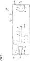
FIG. 1 is a plan view of an interposer which is a wiring structural body produced by a method for producing the wiring structural body according to an embodiment of the present disclosure. -
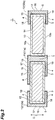
FIG 2 is a cross-sectional view taken along line II-II of the interposer ofFIG. 1 . -
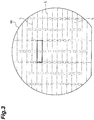
FIG. 3 is a view illustrating the method for producing the interposer ofFIG 1 . -
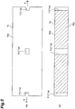
FIGS. 4(a) and 4(b) are views illustrating the method for producing the interposer ofFIG 1 . -
FIGS. 5(a) and 5(b) are views illustrating the method for producing the interposer ofFIG 1 . -
FIGS. 6(a) and 6(b) are views illustrating the method for producing the interposer ofFIG. 1 . -
FIGS. 7(a) and 7(b) are views illustrating the method for producing the interposer ofFIG 1 . -
FIGS. 8(a) and 8(b) are views illustrating the method for producing the interposer ofFIG. 1 . -
FIGS. 9(a) and 9(b) are views illustrating the method for producing the interposer ofFIG 1 . - Hereinafter, an embodiment of the present disclosure will be described in detail with reference to the drawings. In each figure, the same or corresponding components are denoted by the same reference numerals, and redundant description is omitted.
- An interposer (wiring structural body) 1 illustrated in
FIGS. 1 and2 is, for example, a relay substrate used for relaying electrical connection between electronic components having different terminal pitches. The interposer 1 includes a rectangular plate-shaped silicon substrate 10 made of a silicon (Si) crystal. Awiring pattern 3 having a predetermined shape is provided on thesilicon substrate 10. Thewiring pattern 3 includes asurface wiring pattern 4 provided along a firstprincipal surface 10a and a secondprincipal surface 10b of thesilicon substrate 10 and a through-wiring pattern 5 connecting thesurface wiring pattern 4 on the firstprincipal surface 10a side and thesurface wiring pattern 4 on the secondprincipal surface 10b side. InFIGS. 1 and2 , thewiring pattern 3 is schematically illustrated in a simple shape, but actually, thewiring pattern 3 is formed accurately to have a complicated shape. - The
silicon substrate 10 is provided with athrough hole 11 penetrating thesilicon substrate 10 and being opened to the firstprincipal surface 10a and the secondprincipal surface 10b of thesilicon substrate 10. A through-wiring pattern 5 is disposed in the throughhole 11. The throughhole 11 has a quadrangular prism shape extending along a thickness direction D of thesilicon substrate 10. A width of thethrough hole 11 is, for example, 10 µm or more and 100 µm or less. The width of thethrough hole 11 is a width in a direction perpendicular to a penetration direction, and herein, the width of the through hole is a distance between facing two sides. Aninner surface 11a of thethrough hole 11 is entirely along the thickness direction D and intersects the firstprincipal surface 10a and the secondprincipal surface 10b at right angles. -
FIGS. 1 and2 also schematically illustrate the throughhole 11 in a simple shape, but actually, a plurality of the throughholes 11 are provided. For example, in addition to the vertical holes as described above, the throughholes 11 having various shapes such as inclined holes of which penetration directions are inclined with respect to the thickness direction D and bent holes having bent portions may be provided. Theinner surface 11a of the throughhole 11 may have a portion along the thickness direction D as described above and a portion along the direction intersecting the thickness direction D and may have a tapered portion. Alternatively, the entireinner surface 11a may be formed to have a tapered shape. - In addition, at least a portion of the
inner surface 11a of the throughhole 11 may be along a direction intersecting the thickness direction D. For example, the entireinner surface 11a of the throughhole 11 may be along the direction intersecting the thickness direction D (inclined hole). Alternatively, the throughhole 11 may have a first portion where theinner surface 11a is along the first direction and a second portion where theinner surface 11a is along the second direction which intersects the first direction and the thickness direction D (bent hole). - In the
silicon substrate 10, each of a pair ofside surfaces depression 12. Thedepression 12 is formed by cutting a silicon wafer W (refer toFIG. 3 ) on which the throughholes 11 are formed, along dicing lines L passing through the throughholes 11 as described later. Thedepression 12 has a quadrangular prism shape that bisects the throughhole 11 along a plane that passes through the center of the throughhole 11 and is parallel to theside surface 10c. - In the
silicon substrate 10, aninsulating layer 14 is provided on the firstprincipal surface 10a, the secondprincipal surface 10b, theinner surface 11a of the throughhole 11, and theinner surface 12a of thedepression 12. Theinsulating layer 14 is, for example, a silicon oxide film formed by performing thermal oxidation treatment on the surface of thesilicon substrate 10. Theinsulating layer 14 has a thickness of, for example, 1.0 µm or less. - A
boron layer 15 is provided on theinsulating layer 14. Theboron layer 15 is formed along thewiring pattern 3. That is, theboron layer 15 is formed on the insulatinglayer 14 on the firstprincipal surface 10a and the secondprincipal surface 10b along thesurface wiring pattern 4 and is formed on the insulatinglayer 14 on theinner surface 11a of the throughhole 11 and theinner surface 12a of thedepression 12 along the through-wiring pattern 5. In this example, theboron layer 15 is formed over the entire surface of theinsulating layer 14 on theinner surface 11a and theinner surface 12a. Theboron layer 15 formed on the insulatinglayer 14 on theinner surface 11a and theinner surface 12a is continuous with theboron layer 15 formed on the insulatinglayer 14 on the firstprincipal surface 10a and the secondprincipal surface 10b. Theboron layer 15 is isotropically formed with a thickness of several nanometers to several tens of nanometers by a vapor deposition such as a chemical vapor deposition (CVD) epitaxial growth. - A
metal layer 16 is formed on theboron layer 15. Themetal layer 16 has a thickness of, for example, several micrometers to several tens of micrometers. Themetal layer 16 is formed on theboron layer 15 on the firstprincipal surface 10a and the secondprincipal surface 10b along thesurface wiring pattern 4 and is formed on theboron layer 15 on theinner surface 11a of the throughhole 11 and theinner surface 12a of thedepression 12 along the through-wiring pattern 5. In this example, themetal layer 16 is buried in the throughhole 11 and filled in the throughhole 11 without a gap. - The
metal layer 16 is, for example, a plating layer isotropically formed on theboron layer 15 by plating. An example of plating, electroless metal plating may be exemplified. Themetal layer 16 is configured by forming agold layer 18 made of gold and having a thickness of about 0.05 µm on thenickel layer 17 made of nickel and having a thickness of about 5 µm or about 10 µm by, for example, electroless Ni/Au plating. As described above, because thedepression 12 is formed by cutting the throughhole 11, in themetal layer 16 in thedepression 12, thegold layer 18 is not formed on thenickel layer 17, and thenickel layer 17 is exposed to the outer surface. In addition, it is the findings that the present inventors have found that themetal layer 16 is stably formed on theboron layer 15 and that themetal layer 16 is selectively and isotropically formed on theboron layer 15 by plating. - Next, a method for producing an interposer 1 will be described with reference to
FIGS. 3 to 9(b) . In addition, inFIGS. 4(a) to 9(b) ,FIGS. 4(a) ,5(a) ,6(a) ,7(a) ,8(a) , and9(a) are plan views, andFIGS. 4(b) ,5(b) ,6(b) ,7(b) ,8(b) , and9(b) are cross-sectional views taken along line B-B. - As illustrated in
FIG 3 , a silicon wafer W for obtaining a plurality of interposers 1 by cutting along dicing lines L set in a grid shape is prepared. A portion indicated by a thick line inFIG. 3 is to be an interposer 1. Hereinafter, the method for producing the interposer 1 will be described focusing on the thick-line portion. - First, as illustrated in
FIGS. 4(a) and 4(b) , a silicon substrate 10 (silicon wafer W) is prepared. Subsequently, as illustrated inFIGS. 5(a) and 5(b) , a throughhole 11 is formed in thesilicon substrate 10 by reactive ion etching or the like. Subsequently, as illustrated inFIGS. 6(a) and 6(b) , by performing thermal oxidation treatment on a surface of thesilicon substrate 10, an insulatinglayer 14 is formed on a firstprincipal surface 10a and a secondprincipal surface 10b of thesilicon substrate 10 and aninner surface 11a of the through hole 11 (including aninner surface 12a of adepression 12 after cutting) (first step). - Subsequently, as illustrated in
FIGS. 7(a) and 7(b) , aboron layer 15 is isotropically formed on the firstprincipal surface 10a and the secondprincipal surface 10b of thesilicon substrate 10 and theinner surface 11a of the throughhole 11 by CVD epitaxial growth (second step). Subsequently, as illustrated inFIGS. 8(a) and 8(b) , theboron layer 15 is patterned along a region R of awiring pattern 3 by dry etching (second step). - Subsequently, as illustrated in
FIGS. 9(a) and 9(b) , ametal layer 16 is selectively and isotropically formed on theboron layer 15 by plating (third step). More specifically, anickel layer 17 is formed on theboron layer 15 by plating, and after that, agold layer 18 is formed on thenickel layer 17 by plating. Accordingly, thewiring pattern 3 including asurface wiring pattern 4 and a through-wiring pattern 5 is formed. Finally, the silicon wafer W is cut along the dicing lines L to obtain the interposers 1. - As described heretofore, in the method for producing the interposer 1, the
boron layer 15 is formed on the insulatinglayer 14 along the region R for forming thewiring pattern 3, and after that, themetal layer 16 is formed on theboron layer 15 by plating. This configuration is based on the findings that the present inventors have found that themetal layer 16 is selectively and isotropically formed on theboron layer 15 by plating. Therefore, by forming theboron layer 15 accurately by, for example, patterning, thefine wiring pattern 3 can be formed. In addition, in the method for producing the interposer 1, themetal layer 16 is formed on theboron layer 15. This configuration is based on the findings that the present inventors have found that themetal layer 16 is stably formed on theboron layer 15. Therefore, reliability of electrical connection in thewiring pattern 3 can be achieved. Accordingly, in the method for producing the interposer 1, it is possible to achieve both miniaturization of thewiring pattern 3 and reliability of electrical connection in thewiring pattern 3. - In the method for producing the interposer 1, the
boron layer 15 is isotropically formed on the insulatinglayer 14 by CVD epitaxial growth, and after that, theboron layer 15 is patterned along the region R. Therefore, it is possible to accurately and easily form theboron layer 15 along the region R. - In the method for producing the interposer 1, the
nickel layer 17 is formed on theboron layer 15 by plating. Because thenickel layer 17 is easily adhered to theboron layer 15, it is possible to reliably and easily form thenickel layer 17 on theboron layer 15. - In the interposer 1, the
metal layer 16 is formed on the insulatinglayer 14 on theinner surface 11a of the throughhole 11 with theboron layer 15 interposed therebetween. This configuration is based on the findings that the present inventors have found that themetal layer 16 is stably formed on theboron layer 15. As a result, in the interposer 1, electrical connection in the through-wiring pattern 5 is reliably achieved. - In the interposer 1, the
inner surface 11a of the throughhole 11 is along the thickness direction D. In a case where theinner surface 11a is along the thickness direction D, it is difficult to form themetal layer 16 on theinner surface 11a by, for example, a vapor deposition such as evaporation. Because themetal layer 16 is formed on the insulatinglayer 14 on theinner surface 11a with theboron layer 15 interposed therebetween, even in such a case, themetal layer 16 is stably formed on theinner surface 11a, and electrical connection in the through-wiring pattern 5 is reliably achieved. - In the interposer 1, the
inner surface 11a of the throughhole 11 is along a direction intersecting the thickness direction D. In a case where theinner surface 11a is along a direction intersecting the thickness direction D, it is difficult to form themetal layer 16 on theinner surface 11a by, for example, a vapor deposition such as evaporation. Because themetal layer 16 is formed on the insulatinglayer 14 on theinner surface 11a with theboron layer 15 interposed therebetween, even in such a case, themetal layer 16 is stably formed on theinner surface 11a, and electrical connection in the through-wiring pattern 5 is reliably achieved. - In the interposer 1, the width of the through
hole 11 is 10 µm or more and 100 µm or less. Because themetal layer 16 is formed on the insulatinglayer 14 on theinner surface 11a of the throughhole 11 with theboron layer 15 interposed therebetween, even in such a fine throughhole 11, themetal layer 16 is formed on theinner surface 11a of the throughhole 11, and electrical connection in the through-wiring pattern 5 is reliably achieved. - In the interposer 1, the
metal layer 16 is a plating layer. This configuration is based on the findings that the present inventors have found that themetal layer 16 is selectively and isotropically formed on theboron layer 15 by plating. As a result, by forming theboron layer 15 on the insulatinglayer 14 on theinner surface 11a of the throughhole 11, it is possible to reliably form themetal layer 16 on the insulatinglayer 14 on theinner surface 11a of the throughhole 11 with theboron layer 15 interposed therebetween without depending on the shape of the throughhole 11 or the like. Therefore, electrical connection in the through-wiring pattern 5 is more reliably achieved. - In the interposer 1, the
silicon substrate 10 constitutes the interposer 1. Therefore, it is possible to obtain the interposer 1 in which electrical connection in the through-wiring pattern 5 is reliably achieved. - In a case where the
metal layer 16 is formed on the insulatinglayer 14 by using, for example, a vapor deposition such as evaporation or sputtering, in order to facilitate formation of themetal layer 16 on the insulatinglayer 14, it is necessary to form theinner surface 11a of the throughhole 11 in, for example, a tapered shape or the like. On the contrary, in the method for producing the interposer 1, because themetal layer 16 can be selectively and isotropically formed on theboron layer 15 by plating, even in a case where theinner surface 11a is along the thickness direction D, it is possible to stably form themetal layer 16 on theinner surface 11a. As a result, it is not necessary to form theinner surface 11a in a tapered shape, and it is possible to easily produce the interposer 1 having the finer through-wiring pattern 5. - Heretofore, although one embodiment of the present disclosure has been described above, one embodiment of the present disclosure is not limited to the above-described one embodiment. For example, in the above-described embodiment, although the insulating
layer 14 is a silicon oxide film formed by performing thermal oxidation treatment on the surface of thesilicon substrate 10, the insulating layer may be stacked on the surface of thesilicon substrate 10. The insulatinglayer 14 may be formed on the surface of thesilicon substrate 10 including theinner surface 11a of the throughhole 11 along at least the wiring pattern 3 (region R).The insulatinglayer 14 may be formed only in the region along thewiring pattern 3. - The
metal layer 16 may not be embedded in the throughhole 11 and may be provided on theboron layer 15 on theinner surface 11a of the throughhole 11 so that a gap is formed in the throughhole 11. For example, themetal layer 16 may be provided so as to form a gap that is opened to the firstprincipal surface 10a side and the secondprincipal surface 10b side of thesilicon substrate 10 in the throughhole 11. - In the above-described embodiment, the
silicon substrate 10 constitutes the interposer 1. However, thesilicon substrate 10 may constitute a semiconductor device (for example, an optical semiconductor element such as an image sensor). In this case, the through-wiring pattern 5 electrically connects, for example, an electrode which is thesurface wiring pattern 4 on the firstprincipal surface 10a side and a mounting pad which is thesurface wiring pattern 4 on the secondprincipal surface 10b side. In the case of application to an image sensor, from the viewpoint of suppressing a dark current, it is preferable that theboron layer 15 is disposed in the vicinity of a light receiving portion. In a case where thesilicon substrate 10 constitutes a semiconductor device, it is preferable that themetal layer 16 is formed by electroless metal plating in order to avoid electric breakdown. - In the above-described embodiment, the through
hole 11 is provided in thesilicon substrate 10, and the through-wiring pattern 5 is included in thewiring pattern 3. However, the throughhole 11 may not be provided, and the through-wiring pattern 5 may not be included in thewiring pattern 3. Irregularities may be provided on the surface of thesilicon substrate 10, and thewiring pattern 3 may be provided along the irregularities. In the method for producing the interposer 1 according to the embodiment, because theboron layer 15 is isotropically formed by a vapor deposition, even in a case where there are irregularities or the like in the region R, it is possible to reliably form theboron layer 15 along the region R. - 1: interposer (wiring structural body), 3: wiring pattern, 10: silicon substrate, 14: insulating layer, 15: boron layer, 16: metal layer, R: region for forming wiring pattern.
Claims (3)
- A method for producing a wiring structural body provided with a wiring pattern, comprising:a first step of forming an insulating layer on a surface of a silicon substrate along at least a region for forming the wiring pattern;a second step of forming a boron layer on the insulating layer along the region; anda third step of forming a metal layer on the boron layer by plating.
- The method for producing a wiring structural body according to claim 1, wherein, in the second step, the boron layer is isotropically formed on the insulating layer by a vapor deposition, and after that, the boron layer is patterned along the region.
- The method for producing a wiring structural body according to claim 1 or 2, wherein in the third step, a nickel layer is formed on the boron layer by plating.
Applications Claiming Priority (2)
| Application Number | Priority Date | Filing Date | Title |
|---|---|---|---|
| JP2015197522A JP6473405B2 (en) | 2015-10-05 | 2015-10-05 | Manufacturing method of wiring structure |
| PCT/JP2016/075680 WO2017061193A1 (en) | 2015-10-05 | 2016-09-01 | Method for producing wiring structure |
Publications (3)
| Publication Number | Publication Date |
|---|---|
| EP3361494A1 true EP3361494A1 (en) | 2018-08-15 |
| EP3361494A4 EP3361494A4 (en) | 2019-05-22 |
| EP3361494B1 EP3361494B1 (en) | 2020-06-17 |
Family
ID=58487433
Family Applications (1)
| Application Number | Title | Priority Date | Filing Date |
|---|---|---|---|
| EP16853347.9A Active EP3361494B1 (en) | 2015-10-05 | 2016-09-01 | Method for producing wiring structure |
Country Status (6)
| Country | Link |
|---|---|
| US (1) | US11094547B2 (en) |
| EP (1) | EP3361494B1 (en) |
| JP (1) | JP6473405B2 (en) |
| CN (1) | CN108140565B (en) |
| TW (1) | TWI715625B (en) |
| WO (1) | WO2017061193A1 (en) |
Family Cites Families (22)
| Publication number | Priority date | Publication date | Assignee | Title |
|---|---|---|---|---|
| US5116589A (en) * | 1990-06-18 | 1992-05-26 | The United States Of America As Represented By The United States Department Of Energy | High density hexagonal boron nitride prepared by hot isostatic pressing in refractory metal containers |
| US5842387A (en) * | 1994-11-07 | 1998-12-01 | Marcus; Robert B. | Knife blades having ultra-sharp cutting edges and methods of fabrication |
| US6331483B1 (en) | 1998-12-18 | 2001-12-18 | Tokyo Electron Limited | Method of film-forming of tungsten |
| TW411569B (en) * | 1999-01-05 | 2000-11-11 | Ind Tech Res Inst | Method of using the electroless plating technology to fabricate the copper/gold connections in integrated circuits |
| JP3327244B2 (en) * | 1999-03-12 | 2002-09-24 | 日本電気株式会社 | Semiconductor device |
| US6693356B2 (en) * | 2002-03-27 | 2004-02-17 | Texas Instruments Incorporated | Copper transition layer for improving copper interconnection reliability |
| US6933237B2 (en) * | 2002-06-21 | 2005-08-23 | Hewlett-Packard Development Company, L.P. | Substrate etch method and device |
| DE10308855A1 (en) | 2003-02-27 | 2004-09-16 | Infineon Technologies Ag | Semiconductor wafer for electronic components, with integrated circuits in lines and columns for semiconductor chips on wafer top surface with strip-shaped dividing regions between chip integrated circuits |
| US7144803B2 (en) | 2003-04-17 | 2006-12-05 | Semiconductor Research Corporation | Methods of forming boron carbo-nitride layers for integrated circuit devices |
| WO2006117884A1 (en) * | 2005-04-26 | 2006-11-09 | Mitsui Mining & Smelting Co., Ltd. | Al-Ni-B ALLOY WIRING MATERIAL AND DEVICE STRUCTURE USING SAME |
| TW201101476A (en) * | 2005-06-02 | 2011-01-01 | Sony Corp | Semiconductor image sensor module and method of manufacturing the same |
| JP2007113092A (en) * | 2005-10-21 | 2007-05-10 | Seiko Epson Corp | Plating method |
| JP2008115448A (en) * | 2006-11-07 | 2008-05-22 | Seiko Epson Corp | Electroless plating method |
| KR20080061978A (en) * | 2006-12-28 | 2008-07-03 | 주식회사 하이닉스반도체 | Wiring Formation Method of Semiconductor Device |
| US7977791B2 (en) * | 2007-07-09 | 2011-07-12 | Taiwan Semiconductor Manufacturing Company, Ltd. | Selective formation of boron-containing metal cap pre-layer |
| TWI529808B (en) * | 2010-06-10 | 2016-04-11 | Asm國際股份有限公司 | Method for selectively depositing a film on a substrate |
| JP2012077342A (en) * | 2010-09-30 | 2012-04-19 | Yamato Denki Kogyo Kk | Method for forming metal pattern |
| JP2012119381A (en) * | 2010-11-29 | 2012-06-21 | Toshiba Corp | Semiconductor device and method of manufacturing semiconductor device |
| US8461043B2 (en) * | 2011-04-11 | 2013-06-11 | Micron Technology, Inc. | Barrier layer for integrated circuit contacts |
| JP5559120B2 (en) * | 2011-09-22 | 2014-07-23 | 株式会社東芝 | Nonvolatile semiconductor memory device |
| CN110004429B (en) * | 2012-03-27 | 2021-08-31 | 诺发系统公司 | Tungsten Feature Fill |
| WO2013158986A2 (en) * | 2012-04-19 | 2013-10-24 | Carnegie Mellon University | A metal-semiconductor-metal (msm) heterojunction diode |
-
2015
- 2015-10-05 JP JP2015197522A patent/JP6473405B2/en active Active
-
2016
- 2016-09-01 US US15/765,528 patent/US11094547B2/en active Active
- 2016-09-01 WO PCT/JP2016/075680 patent/WO2017061193A1/en not_active Ceased
- 2016-09-01 CN CN201680058496.5A patent/CN108140565B/en active Active
- 2016-09-01 EP EP16853347.9A patent/EP3361494B1/en active Active
- 2016-09-08 TW TW105129031A patent/TWI715625B/en active
Also Published As
| Publication number | Publication date |
|---|---|
| CN108140565B (en) | 2022-08-05 |
| US11094547B2 (en) | 2021-08-17 |
| US20190080912A1 (en) | 2019-03-14 |
| CN108140565A (en) | 2018-06-08 |
| TWI715625B (en) | 2021-01-11 |
| WO2017061193A1 (en) | 2017-04-13 |
| JP6473405B2 (en) | 2019-02-20 |
| EP3361494A4 (en) | 2019-05-22 |
| JP2017073417A (en) | 2017-04-13 |
| TW201724434A (en) | 2017-07-01 |
| EP3361494B1 (en) | 2020-06-17 |
Similar Documents
| Publication | Publication Date | Title |
|---|---|---|
| US9585254B2 (en) | Electronic device | |
| US9445503B2 (en) | Carrier device, electrical device having a carrier device and method for producing same | |
| TWI666737B (en) | Wiring substrate, method of manufacturing the same and electronic component device | |
| US9927499B2 (en) | Semiconductor device | |
| TWI508240B (en) | Laminated wiring board | |
| JP2012248754A (en) | Method of manufacturing semiconductor device and semiconductor device | |
| US8786099B2 (en) | Wiring substrate and semiconductor package | |
| US11094547B2 (en) | Method for producing wiring structure | |
| US10163775B2 (en) | Electronic device | |
| EP3361499B1 (en) | Wiring structure and method for producing wiring structure | |
| JP2016157901A (en) | Electronic device | |
| KR101411734B1 (en) | Fabricating method of semiconductor device having through silicon via and semiconductor device therof | |
| JP2015149314A (en) | Semiconductor device and manufacturing method thereof | |
| US20140374853A1 (en) | Component including means for reducing assembly-related mechanical stresses and methods for manufacturing same | |
| JP2009267098A (en) | Semiconductor apparatus and method of manufacturing the same | |
| US20130257420A1 (en) | Sensor, method for producing a sensor and method for mounting a sensor | |
| JP2013004572A (en) | Semiconductor device manufacturing method | |
| US11373958B2 (en) | Semiconductor device and semiconductor device manufacturing method for prevention of metallic diffusion into a semiconductor substrate | |
| JP2016143782A (en) | Electronic device | |
| JP2016100555A (en) | Electronic equipment | |
| JP2019197911A (en) | Electronic equipment | |
| JP2017135294A (en) | Semiconductor device substrate, semiconductor device substrate manufacturing method, semiconductor device, and semiconductor device manufacturing method | |
| JP2017135294A6 (en) | Semiconductor device substrate, semiconductor device substrate manufacturing method, semiconductor device, and semiconductor device manufacturing method |
Legal Events
| Date | Code | Title | Description |
|---|---|---|---|
| STAA | Information on the status of an ep patent application or granted ep patent |
Free format text: STATUS: THE INTERNATIONAL PUBLICATION HAS BEEN MADE |
|
| PUAI | Public reference made under article 153(3) epc to a published international application that has entered the european phase |
Free format text: ORIGINAL CODE: 0009012 |
|
| STAA | Information on the status of an ep patent application or granted ep patent |
Free format text: STATUS: REQUEST FOR EXAMINATION WAS MADE |
|
| 17P | Request for examination filed |
Effective date: 20180201 |
|
| AK | Designated contracting states |
Kind code of ref document: A1 Designated state(s): AL AT BE BG CH CY CZ DE DK EE ES FI FR GB GR HR HU IE IS IT LI LT LU LV MC MK MT NL NO PL PT RO RS SE SI SK SM TR |
|
| AX | Request for extension of the european patent |
Extension state: BA ME |
|
| DAV | Request for validation of the european patent (deleted) | ||
| DAX | Request for extension of the european patent (deleted) | ||
| A4 | Supplementary search report drawn up and despatched |
Effective date: 20190425 |
|
| RIC1 | Information provided on ipc code assigned before grant |
Ipc: H01L 23/12 20060101ALI20190417BHEP Ipc: C23C 18/16 20060101ALI20190417BHEP Ipc: H01L 23/522 20060101ALI20190417BHEP Ipc: H01L 21/48 20060101ALI20190417BHEP Ipc: C23C 18/18 20060101ALI20190417BHEP Ipc: H01L 21/768 20060101ALI20190417BHEP Ipc: H01L 21/3205 20060101ALI20190417BHEP Ipc: H01L 23/14 20060101ALI20190417BHEP Ipc: H01L 23/498 20060101ALI20190417BHEP Ipc: H01L 21/288 20060101AFI20190417BHEP |
|
| RIC1 | Information provided on ipc code assigned before grant |
Ipc: C23C 18/18 20060101ALI20191203BHEP Ipc: H01L 23/12 20060101ALI20191203BHEP Ipc: H01L 23/14 20060101ALI20191203BHEP Ipc: H01L 21/288 20060101AFI20191203BHEP Ipc: H01L 21/768 20060101ALI20191203BHEP Ipc: H01L 23/498 20060101ALI20191203BHEP Ipc: H01L 21/3205 20060101ALI20191203BHEP Ipc: H01L 21/48 20060101ALI20191203BHEP Ipc: C23C 18/16 20060101ALI20191203BHEP Ipc: H01L 23/522 20060101ALI20191203BHEP |
|
| GRAP | Despatch of communication of intention to grant a patent |
Free format text: ORIGINAL CODE: EPIDOSNIGR1 |
|
| STAA | Information on the status of an ep patent application or granted ep patent |
Free format text: STATUS: GRANT OF PATENT IS INTENDED |
|
| INTG | Intention to grant announced |
Effective date: 20200113 |
|
| GRAS | Grant fee paid |
Free format text: ORIGINAL CODE: EPIDOSNIGR3 |
|
| GRAA | (expected) grant |
Free format text: ORIGINAL CODE: 0009210 |
|
| STAA | Information on the status of an ep patent application or granted ep patent |
Free format text: STATUS: THE PATENT HAS BEEN GRANTED |
|
| AK | Designated contracting states |
Kind code of ref document: B1 Designated state(s): AL AT BE BG CH CY CZ DE DK EE ES FI FR GB GR HR HU IE IS IT LI LT LU LV MC MK MT NL NO PL PT RO RS SE SI SK SM TR |
|
| REG | Reference to a national code |
Ref country code: GB Ref legal event code: FG4D |
|
| REG | Reference to a national code |
Ref country code: CH Ref legal event code: EP |
|
| REG | Reference to a national code |
Ref country code: IE Ref legal event code: FG4D |
|
| REG | Reference to a national code |
Ref country code: DE Ref legal event code: R096 Ref document number: 602016038470 Country of ref document: DE |
|
| REG | Reference to a national code |
Ref country code: AT Ref legal event code: REF Ref document number: 1282361 Country of ref document: AT Kind code of ref document: T Effective date: 20200715 |
|
| PG25 | Lapsed in a contracting state [announced via postgrant information from national office to epo] |
Ref country code: FI Free format text: LAPSE BECAUSE OF FAILURE TO SUBMIT A TRANSLATION OF THE DESCRIPTION OR TO PAY THE FEE WITHIN THE PRESCRIBED TIME-LIMIT Effective date: 20200617 Ref country code: SE Free format text: LAPSE BECAUSE OF FAILURE TO SUBMIT A TRANSLATION OF THE DESCRIPTION OR TO PAY THE FEE WITHIN THE PRESCRIBED TIME-LIMIT Effective date: 20200617 Ref country code: LT Free format text: LAPSE BECAUSE OF FAILURE TO SUBMIT A TRANSLATION OF THE DESCRIPTION OR TO PAY THE FEE WITHIN THE PRESCRIBED TIME-LIMIT Effective date: 20200617 Ref country code: GR Free format text: LAPSE BECAUSE OF FAILURE TO SUBMIT A TRANSLATION OF THE DESCRIPTION OR TO PAY THE FEE WITHIN THE PRESCRIBED TIME-LIMIT Effective date: 20200918 Ref country code: NO Free format text: LAPSE BECAUSE OF FAILURE TO SUBMIT A TRANSLATION OF THE DESCRIPTION OR TO PAY THE FEE WITHIN THE PRESCRIBED TIME-LIMIT Effective date: 20200917 |
|
| REG | Reference to a national code |
Ref country code: LT Ref legal event code: MG4D |
|
| REG | Reference to a national code |
Ref country code: NL Ref legal event code: MP Effective date: 20200617 |
|
| PG25 | Lapsed in a contracting state [announced via postgrant information from national office to epo] |
Ref country code: BG Free format text: LAPSE BECAUSE OF FAILURE TO SUBMIT A TRANSLATION OF THE DESCRIPTION OR TO PAY THE FEE WITHIN THE PRESCRIBED TIME-LIMIT Effective date: 20200917 Ref country code: LV Free format text: LAPSE BECAUSE OF FAILURE TO SUBMIT A TRANSLATION OF THE DESCRIPTION OR TO PAY THE FEE WITHIN THE PRESCRIBED TIME-LIMIT Effective date: 20200617 Ref country code: RS Free format text: LAPSE BECAUSE OF FAILURE TO SUBMIT A TRANSLATION OF THE DESCRIPTION OR TO PAY THE FEE WITHIN THE PRESCRIBED TIME-LIMIT Effective date: 20200617 Ref country code: HR Free format text: LAPSE BECAUSE OF FAILURE TO SUBMIT A TRANSLATION OF THE DESCRIPTION OR TO PAY THE FEE WITHIN THE PRESCRIBED TIME-LIMIT Effective date: 20200617 |
|
| REG | Reference to a national code |
Ref country code: AT Ref legal event code: MK05 Ref document number: 1282361 Country of ref document: AT Kind code of ref document: T Effective date: 20200617 |
|
| PG25 | Lapsed in a contracting state [announced via postgrant information from national office to epo] |
Ref country code: AL Free format text: LAPSE BECAUSE OF FAILURE TO SUBMIT A TRANSLATION OF THE DESCRIPTION OR TO PAY THE FEE WITHIN THE PRESCRIBED TIME-LIMIT Effective date: 20200617 Ref country code: NL Free format text: LAPSE BECAUSE OF FAILURE TO SUBMIT A TRANSLATION OF THE DESCRIPTION OR TO PAY THE FEE WITHIN THE PRESCRIBED TIME-LIMIT Effective date: 20200617 |
|
| PG25 | Lapsed in a contracting state [announced via postgrant information from national office to epo] |
Ref country code: AT Free format text: LAPSE BECAUSE OF FAILURE TO SUBMIT A TRANSLATION OF THE DESCRIPTION OR TO PAY THE FEE WITHIN THE PRESCRIBED TIME-LIMIT Effective date: 20200617 Ref country code: ES Free format text: LAPSE BECAUSE OF FAILURE TO SUBMIT A TRANSLATION OF THE DESCRIPTION OR TO PAY THE FEE WITHIN THE PRESCRIBED TIME-LIMIT Effective date: 20200617 Ref country code: SM Free format text: LAPSE BECAUSE OF FAILURE TO SUBMIT A TRANSLATION OF THE DESCRIPTION OR TO PAY THE FEE WITHIN THE PRESCRIBED TIME-LIMIT Effective date: 20200617 Ref country code: EE Free format text: LAPSE BECAUSE OF FAILURE TO SUBMIT A TRANSLATION OF THE DESCRIPTION OR TO PAY THE FEE WITHIN THE PRESCRIBED TIME-LIMIT Effective date: 20200617 Ref country code: CZ Free format text: LAPSE BECAUSE OF FAILURE TO SUBMIT A TRANSLATION OF THE DESCRIPTION OR TO PAY THE FEE WITHIN THE PRESCRIBED TIME-LIMIT Effective date: 20200617 Ref country code: IT Free format text: LAPSE BECAUSE OF FAILURE TO SUBMIT A TRANSLATION OF THE DESCRIPTION OR TO PAY THE FEE WITHIN THE PRESCRIBED TIME-LIMIT Effective date: 20200617 Ref country code: RO Free format text: LAPSE BECAUSE OF FAILURE TO SUBMIT A TRANSLATION OF THE DESCRIPTION OR TO PAY THE FEE WITHIN THE PRESCRIBED TIME-LIMIT Effective date: 20200617 Ref country code: PT Free format text: LAPSE BECAUSE OF FAILURE TO SUBMIT A TRANSLATION OF THE DESCRIPTION OR TO PAY THE FEE WITHIN THE PRESCRIBED TIME-LIMIT Effective date: 20201019 |
|
| PG25 | Lapsed in a contracting state [announced via postgrant information from national office to epo] |
Ref country code: PL Free format text: LAPSE BECAUSE OF FAILURE TO SUBMIT A TRANSLATION OF THE DESCRIPTION OR TO PAY THE FEE WITHIN THE PRESCRIBED TIME-LIMIT Effective date: 20200617 Ref country code: SK Free format text: LAPSE BECAUSE OF FAILURE TO SUBMIT A TRANSLATION OF THE DESCRIPTION OR TO PAY THE FEE WITHIN THE PRESCRIBED TIME-LIMIT Effective date: 20200617 Ref country code: IS Free format text: LAPSE BECAUSE OF FAILURE TO SUBMIT A TRANSLATION OF THE DESCRIPTION OR TO PAY THE FEE WITHIN THE PRESCRIBED TIME-LIMIT Effective date: 20201017 |
|
| REG | Reference to a national code |
Ref country code: DE Ref legal event code: R097 Ref document number: 602016038470 Country of ref document: DE |
|
| PLBE | No opposition filed within time limit |
Free format text: ORIGINAL CODE: 0009261 |
|
| STAA | Information on the status of an ep patent application or granted ep patent |
Free format text: STATUS: NO OPPOSITION FILED WITHIN TIME LIMIT |
|
| PG25 | Lapsed in a contracting state [announced via postgrant information from national office to epo] |
Ref country code: DK Free format text: LAPSE BECAUSE OF FAILURE TO SUBMIT A TRANSLATION OF THE DESCRIPTION OR TO PAY THE FEE WITHIN THE PRESCRIBED TIME-LIMIT Effective date: 20200617 |
|
| REG | Reference to a national code |
Ref country code: CH Ref legal event code: PL |
|
| 26N | No opposition filed |
Effective date: 20210318 |
|
| PG25 | Lapsed in a contracting state [announced via postgrant information from national office to epo] |
Ref country code: SI Free format text: LAPSE BECAUSE OF FAILURE TO SUBMIT A TRANSLATION OF THE DESCRIPTION OR TO PAY THE FEE WITHIN THE PRESCRIBED TIME-LIMIT Effective date: 20200617 |
|
| REG | Reference to a national code |
Ref country code: BE Ref legal event code: MM Effective date: 20200930 |
|
| PG25 | Lapsed in a contracting state [announced via postgrant information from national office to epo] |
Ref country code: LU Free format text: LAPSE BECAUSE OF NON-PAYMENT OF DUE FEES Effective date: 20200901 |
|
| PG25 | Lapsed in a contracting state [announced via postgrant information from national office to epo] |
Ref country code: IE Free format text: LAPSE BECAUSE OF NON-PAYMENT OF DUE FEES Effective date: 20200901 Ref country code: LI Free format text: LAPSE BECAUSE OF NON-PAYMENT OF DUE FEES Effective date: 20200930 Ref country code: BE Free format text: LAPSE BECAUSE OF NON-PAYMENT OF DUE FEES Effective date: 20200930 Ref country code: CH Free format text: LAPSE BECAUSE OF NON-PAYMENT OF DUE FEES Effective date: 20200930 |
|
| PG25 | Lapsed in a contracting state [announced via postgrant information from national office to epo] |
Ref country code: TR Free format text: LAPSE BECAUSE OF FAILURE TO SUBMIT A TRANSLATION OF THE DESCRIPTION OR TO PAY THE FEE WITHIN THE PRESCRIBED TIME-LIMIT Effective date: 20200617 Ref country code: MT Free format text: LAPSE BECAUSE OF FAILURE TO SUBMIT A TRANSLATION OF THE DESCRIPTION OR TO PAY THE FEE WITHIN THE PRESCRIBED TIME-LIMIT Effective date: 20200617 Ref country code: CY Free format text: LAPSE BECAUSE OF FAILURE TO SUBMIT A TRANSLATION OF THE DESCRIPTION OR TO PAY THE FEE WITHIN THE PRESCRIBED TIME-LIMIT Effective date: 20200617 |
|
| PG25 | Lapsed in a contracting state [announced via postgrant information from national office to epo] |
Ref country code: MK Free format text: LAPSE BECAUSE OF FAILURE TO SUBMIT A TRANSLATION OF THE DESCRIPTION OR TO PAY THE FEE WITHIN THE PRESCRIBED TIME-LIMIT Effective date: 20200617 Ref country code: MC Free format text: LAPSE BECAUSE OF FAILURE TO SUBMIT A TRANSLATION OF THE DESCRIPTION OR TO PAY THE FEE WITHIN THE PRESCRIBED TIME-LIMIT Effective date: 20200617 |
|
| P01 | Opt-out of the competence of the unified patent court (upc) registered |
Effective date: 20230509 |
|
| PGFP | Annual fee paid to national office [announced via postgrant information from national office to epo] |
Ref country code: DE Payment date: 20250730 Year of fee payment: 10 |
|
| PGFP | Annual fee paid to national office [announced via postgrant information from national office to epo] |
Ref country code: GB Payment date: 20250731 Year of fee payment: 10 |
|
| PGFP | Annual fee paid to national office [announced via postgrant information from national office to epo] |
Ref country code: FR Payment date: 20250808 Year of fee payment: 10 |
|
| REG | Reference to a national code |
Ref country code: DE Ref legal event code: R079 Ref document number: 602016038470 Country of ref document: DE Free format text: PREVIOUS MAIN CLASS: H01L0021288000 Ipc: H10D0064010000 |