EP3359929B1 - Dynamische bandbreitenkontrolle einer lock-in detektion für srs abbildungsverfahren - Google Patents
Dynamische bandbreitenkontrolle einer lock-in detektion für srs abbildungsverfahren Download PDFInfo
- Publication number
- EP3359929B1 EP3359929B1 EP16778412.3A EP16778412A EP3359929B1 EP 3359929 B1 EP3359929 B1 EP 3359929B1 EP 16778412 A EP16778412 A EP 16778412A EP 3359929 B1 EP3359929 B1 EP 3359929B1
- Authority
- EP
- European Patent Office
- Prior art keywords
- microscope
- scan
- bandwidth
- frequency value
- lock
- Prior art date
- Legal status (The legal status is an assumption and is not a legal conclusion. Google has not performed a legal analysis and makes no representation as to the accuracy of the status listed.)
- Active
Links
Images



Classifications
-
- G—PHYSICS
- G01—MEASURING; TESTING
- G01J—MEASUREMENT OF INTENSITY, VELOCITY, SPECTRAL CONTENT, POLARISATION, PHASE OR PULSE CHARACTERISTICS OF INFRARED, VISIBLE OR ULTRAVIOLET LIGHT; COLORIMETRY; RADIATION PYROMETRY
- G01J1/00—Photometry, e.g. photographic exposure meter
- G01J1/42—Photometry, e.g. photographic exposure meter using electric radiation detectors
- G01J1/44—Electric circuits
-
- G—PHYSICS
- G01—MEASURING; TESTING
- G01J—MEASUREMENT OF INTENSITY, VELOCITY, SPECTRAL CONTENT, POLARISATION, PHASE OR PULSE CHARACTERISTICS OF INFRARED, VISIBLE OR ULTRAVIOLET LIGHT; COLORIMETRY; RADIATION PYROMETRY
- G01J3/00—Spectrometry; Spectrophotometry; Monochromators; Measuring colours
- G01J3/02—Details
- G01J3/027—Control of working procedures of a spectrometer; Failure detection; Bandwidth calculation
-
- G—PHYSICS
- G01—MEASURING; TESTING
- G01J—MEASUREMENT OF INTENSITY, VELOCITY, SPECTRAL CONTENT, POLARISATION, PHASE OR PULSE CHARACTERISTICS OF INFRARED, VISIBLE OR ULTRAVIOLET LIGHT; COLORIMETRY; RADIATION PYROMETRY
- G01J3/00—Spectrometry; Spectrophotometry; Monochromators; Measuring colours
- G01J3/28—Investigating the spectrum
- G01J3/44—Raman spectrometry; Scattering spectrometry ; Fluorescence spectrometry
-
- G—PHYSICS
- G02—OPTICS
- G02B—OPTICAL ELEMENTS, SYSTEMS OR APPARATUS
- G02B21/00—Microscopes
- G02B21/0004—Microscopes specially adapted for specific applications
- G02B21/002—Scanning microscopes
- G02B21/0024—Confocal scanning microscopes (CSOMs) or confocal "macroscopes"; Accessories which are not restricted to use with CSOMs, e.g. sample holders
- G02B21/008—Details of detection or image processing, including general computer control
- G02B21/0084—Details of detection or image processing, including general computer control time-scale detection, e.g. strobed, ultra-fast, heterodyne detection
-
- G—PHYSICS
- G01—MEASURING; TESTING
- G01J—MEASUREMENT OF INTENSITY, VELOCITY, SPECTRAL CONTENT, POLARISATION, PHASE OR PULSE CHARACTERISTICS OF INFRARED, VISIBLE OR ULTRAVIOLET LIGHT; COLORIMETRY; RADIATION PYROMETRY
- G01J1/00—Photometry, e.g. photographic exposure meter
- G01J1/42—Photometry, e.g. photographic exposure meter using electric radiation detectors
- G01J1/44—Electric circuits
- G01J2001/4406—Plural ranges in circuit, e.g. switchable ranges; Adjusting sensitivity selecting gain values
Definitions
- the present invention relates to an electric circuit for a microscope and a microscope with such an electric circuit.
- the subject-matter according to the invention is preferably useful in connection with stimulated Raman scattering microscopy (SRS) [1, 2] and provides an automatic adaptable lock-in detection bandwidth (or time-constant) for optimal imaging for various imaging settings.
- SRS stimulated Raman scattering microscopy
- CARS coherent Raman scattering microscopy
- CSRS coherent Stokes Raman scattering
- RKES Raman-induced Kerr-effect scattering
- SRS stimulated Raman scattering
- CRSM CRSM-like CRSM
- the technique of CRSM consists of two pulsed (with frequencies ranging typically from 1-100 MHz) optical fields with pulse widths ranging from 100 fs-20 ps of different wavelengths routed through a confocal microscope system and tightly focused on a sample of interest.
- the beam routing and the focusing optics are made such that the two optical fields overlap spatially and temporally at the sample.
- one of the two beams is either intensity modulated or frequency modulated or polarization modulated with a specific frequency ⁇ , typically in kHz to MHz range, before it interacts with the other optical field in the sample.
- a typical SRS microscope system 20 is depicted in Figure 1 .
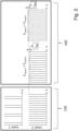
- Two pulsed laser sources (Laser 1 and Laser 2) generate the so called “Stokes” and the "pump” beams for SRS imaging, respectively (see Figure 2 , window 100, where an intensity is shown over time t).
- the laser source with smaller wavelength is designated as the "pump” and the laser with longer wavelength is designated as the "Stokes” beam in the CRSM literature.
- One of the beams (Laser 1) is amplitude modulated with the help of a modulator 3, e.g. an AOM (acousto-optic modulator) or EOM (electro-optic modulator), and combined collinearly with the second laser source (Laser 2) using a dichroic 4.
- the modulator 3 is driven by a RF drive 9 providing a RF frequency signal.
- the temporal overlap of the two laser sources is ensured with the help of a - preferably variable - optical delay stage 5.
- the combined beams travel through a scanning-device or laser-scanning (confocal) microscope 6 and interact with the sample under test at the focus of a microscope objective (not shown). Behind the sample the beam of Laser 1 is blocked by a blocking filter 11.
- the light of Laser 2 acquires a tiny amplitude modulation whose frequency corresponds to the modulation frequency of the light of Laser 1 (see Figure 2 , window 200).
- the light of the Laser 2 could gain or lose energy depending on its relative (to the light of the Laser 1) wavelength. If the wavelength of Laser 2 is smaller than the wavelength of Laser 1, i.e. ⁇ Laser2 ⁇ ⁇ Laser2 , there is an intensity loss I SRL , otherwise a gain I SRG .
- This miniscule gain or loss in Laser 2 is detected with the help of a sensitive detector 7 and signal extraction electronics 8.
- the latter electronic unit can comprise a lock-in amplifier/mixer; the SRS signal is demodulated using the R drive frequency of the modulator 3 as the local oscillator. The resultant signal is routed for image display, storage or analysis 10.
- a lock-in amplifier is an important component of the detection electronics required for extraction of modulated SRS signals.
- SRS detection has been implemented using envelope detection electronics [6]
- use of lock-in detection provides flexible detection bandwidth (implies, varied laser scan frequencies) and higher signal linearity.
- a basic lock-in amplifier 300 comprises an electronic mixer 301 which takes as its input an amplitude modulated signal s and a reference clock signal r. It provides as an output the demodulated signal of s at the reference frequency provided by r.
- commercially available lock-in amplifiers can provide some amount of signal amplification 303 and filtering 302 at the input and/or output ports.
- the frequency bandwidth of the extracted signal o depends on the bandwidth setting BW of the filter 302 at the output stage of the mixer. This bandwidth setting typically ranges from a few tenths of Hz to multiple MHz (or equivalently, a few tens of seconds to a few nanoseconds).
- XP055327869 discloses an SRS-microscope including a lock-in amplifier.
- the output from the photo-diode is fed into the input of the lock-in amplifier, coarsely filtered with a band pass filter around the modulation frequency, and mixed with a reference signal from the modulator.
- the input signal and the reference signal are mixed and fed into a low pass filter.
- a high-frequency lock-in amplifier is used to demodulate the Stokes-intensity. Update rates can be made as short as possible (down to 10 microseconds) to match the pixel-dwell-time of the microscope.
- WO 2011/162787 A1 also shows an SRS-microscope wherein the bandwidth of the filter is inversely proportional to the integration time constant which equals a pixel-dwell-time.
- WO 2014/205007 A1 also discloses an SRS-detection system wherein the output bandwidth of the final low-pass filter of a lock-in amplifier is matched to the maximal acquisition rate.
- Other acquisition parameters which could be modified based on the imaging requirements include laser-scan/stage-scan speed, objective magnification, objective numerical aperture, image scan format (pixel size), image scan width (physical image size), pixel dwell time, zoom, etc. Changing any of these values would lead to a different bandwidth of the modulated signal. If the lock-in time-constant is fixed, varying these parameters could deteriorate image quality.
- an electric circuit for a microscope in particular for a Coherent Raman scattering microscope (CRSM), a Coherent anti-Stokes Raman scattering (CARS) microscope, a coherent Stokes Raman scattering (CSRS) microscope, a Raman-induced Kerr-effect scattering (RIKES) microscope, a stimulated Raman scattering (SRS) microscope or a pump-probe microscope is provided, the electric circuit comprising the features defined in claim 1.
- CRSM Coherent Raman scattering microscope
- CARS Coherent anti-Stokes Raman scattering
- CSRS coherent Stokes Raman scattering
- RKES Raman-induced Kerr-effect scattering
- SRS stimulated Raman scattering
- the present invention provides the advantage that the bandwidth of the lock-in amplifier can be adapted to the current setting such that a maximal measurement bandwidth spectrum is obtained as the output signal for further signal and/or image processing.
- This invention describes a method and an apparatus for implementing e.g. stimulated Raman scattering microscopy (SRS) with an automatic adaptable lock-in detection bandwidth (or time-constant) for optimal imaging for various imaging settings.
- SRS stimulated Raman scattering microscopy
- One aspect of this invention is to provide a device and a method in which the lock-in bandwidth/time-constant is automatically adapted (increased or decreased) to deliver a high quality image and/or the best possible image for a given set of image acquisition parameters.
- the described apparatus can be directly applied for other lock-in based imaging techniques such as OHD-RIKES [2], and pump-probe microscopy techniques [4].
- the at least one parameter of a current setting of the microscope is at least one of a pixel dwell-time, a laser-scan speed, a stage-scan speed, an objective magnification, an objective numerical aperture, an image scan format or a pixel size, an image scan width or a physical image size, and a zoom value.
- the function of the at least one parameter of a current setting of the microscope is at least one of inversely proportional to the pixel dwell-time, proportional to the laser-scan speed, proportional to the stage-scan speed, inversely proportional to the objective magnification, proportional to the objective numerical aperture, proportional to the image scan format or the pixel size, proportional to the image scan width or the physical image size, and inversely proportional to the zoom value.
- Using these parameters allows for easily adapting the measurement bandwidth to the current microscope setting.
- the dynamic bandwidth controller unit is adapted to control the low bandwidth frequency value and/or the high bandwidth frequency value of the lock-in amplifier depending on a potential highest temporal frequency in a demodulated signal, i.e. to set the low bandwidth frequency value and/or the high bandwidth frequency value of the lock-in amplifier to a value depending on said potential highest temporal frequency.
- the value is equal to said potential highest temporal frequency or differs at most 10%, 20%, 30%, 40% or 50% from said potential highest temporal frequency. Thus, a good suitable bandwidth spectrum is obtained.
- the dynamic bandwidth controller unit is adapted to control the low bandwidth frequency value and/or the high bandwidth frequency value of the lock-in amplifier depending on at least one of a wavelength ⁇ of light being focused onto an object, a numerical aperture NA MO of a microscope objective, a system dependent length F Sys which depends on a magnification of the microscope optics, a magnification M MO of the microscope objective, a value Zoom representing an additional - preferably variable settable - magnification of a beam path of the microscope, a duty cycle fill of the laser scan, and a scan frequency f scan . This allow for precisely tuning the bandwidth.
- the dynamic bandwidth controller unit comprises a control circuit functionality which calculates the low bandwidth frequency value and/or the high bandwidth frequency value as the function of parameters of a current setting of the microscope, wherein the calculated low bandwidth frequency value and/or the high bandwidth frequency value is set in the lock-in amplifier and at least one image acquisition is conducted and the measurement bandwidth spectrum of the acquired signal is analysed.
- the dynamic bandwidth controller unit can be formed as a hardware and/or software module, in particular as an ASIC (Application Specific Integrated Circuit) or in a FPGA (Field Programmable Gated Array) or DSP (Digital Signal Processor).
- ASIC Application Specific Integrated Circuit
- FPGA Field Programmable Gated Array
- DSP Digital Signal Processor
- the pixel width w pixel is determined by the magnification of (a) the objective and (b) the relay optics in the confocal scanner and also on length across which the laser light is scanned, which is given by the "Zoom" parameter in a typical commercial laser scanning microscope system.
- the pixel dwell-time t pixel is determined by the frequency of the laser scan, the number of pixels in a single line and the time it takes to scan a single line.
- w pixel F Sys Zoom ⁇ M MO N pixels
- v transit F Sys ⁇ f scan Zoom ⁇ M MO .
- f High F Sys ⁇ f scan ⁇ NA MO 1.22 ⁇ ⁇ Zoom ⁇ M MO ⁇ fill
- the frequency content of the demodulated signal depends on the various system and scan parameters. If any of these parameters change, the frequency content in the signal is bound to change.
- the output low-pass filter should have a bandwidth that is broad enough to let f High through; it should not be too broad otherwise one would have noisy images with the noise coming from the frequency spectrum beyond f High .
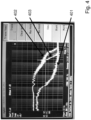
- Figure 4 is a screenshot of the signal in frequency domain as measured with an Agilent spectrum analyser (Model E7401A).
- Line 401 corresponds to the baseline noise curve with no light incident on the detector.
- Line 402 corresponds to the signal that is generated with the zoom parameter set to 0.75.
- Line 403 corresponds to the signal with the zoom parameter set to 1.0.
- an electronic circuit or a software module or a combination of hardware/software module(s) be used which take(s) into account the changes in the scan parameters that might be initiated by a user of the microscope and modify (modifies) the output low-pass filters' bandwidth to let the highest possible signal frequencies through for further processing or display or storage.
- FIG. 5 A pictorial representation of the concept of the present invention is shown in Figure 5 .
- a commercial lock-in UHFLI from Zurich Instruments AG, Zurich, Switzerland along with a software module 500 was used; the latter determines the scan parameters P, calculates the bandwidth values BW and sets this value in the lock-in amplifier unit 300.
Landscapes
- Physics & Mathematics (AREA)
- Spectroscopy & Molecular Physics (AREA)
- General Physics & Mathematics (AREA)
- Engineering & Computer Science (AREA)
- Computer Vision & Pattern Recognition (AREA)
- General Engineering & Computer Science (AREA)
- Chemical & Material Sciences (AREA)
- Analytical Chemistry (AREA)
- Optics & Photonics (AREA)
- Microscoopes, Condenser (AREA)
- Investigating, Analyzing Materials By Fluorescence Or Luminescence (AREA)
- Train Traffic Observation, Control, And Security (AREA)
Claims (6)
- Elektrische Schaltung für ein Mikroskop (20), wobei die elektrische Schaltung einen Lock-in-Verstärker (300) umfasst, wobei der Lock-in-Verstärker (300) umfassteinen Eingang für ein Eingangssignal (s),einen Eingang für ein Referenzsignal (r),einen Ausgang für ein Ausgangssignal (0),und eine Bandbreitenfiltervorrichtung (302),wobei die Bandbreitenfiltervorrichtung (302) dazu eingerichtet ist, dass ein niedriger Bandbreitenfrequenzwert und/oder hoher Bandbreitenfrequenzwert variabel einstellbar ist, wobei die elektrische Schaltung eine dynamische Bandbreitensteuereinheit (500) aufweist, in die Parameter (P) einer aktuellen Einstellung des Mikroskops (20) eingegeben werden, wobei die dynamische Bandbreitensteuereinheit (500) dazu eingerichtet ist, den niedrigen Bandbreitenfrequenzwert und/oder den hohen Bandbreitenfrequenzwert des Lock-in-Verstärkers (300) als eine Funktion der Parameter (P) einer aktuellen Einstellung des Mikroskops (20) zu steuern, wobei die dynamische Bandbreitensteuereinheit (500) dazu eingerichtet ist, den niedrigen Bandbreitenfrequenzwert und/oder den hohen Bandbreitenfrequenzwert des Lock-in-Verstärkers (300) in Abhängigkeit von einer potenziellen höchsten zeitlichen Frequenz in einem demodulierten Signal zu steuern, wobei die potenzielle höchste zeitliche Frequenz in dem demodulierten Signal durch die folgende Formel berechnet wird
 mit:einer Wellenlänge λ von Licht, das auf ein Objekt fokussiert ist,einer numerischen Apertur NAMO eines Mikroskopobjektivs,einer systemabhängigen Länge Fsys, die von einer Vergrößerung der Mikroskopoptik abhängt,einer Vergrößerung MMO des Mikroskopobjektivs,einem Wert Zoom, der eine zusätzliche Vergrößerung eines Strahlengangs des Mikroskops repräsentiert,einem Tastverhältnis fill des Laserscans,einer Abtastfrequenz fscan.
 - Elektrische Schaltung nach Anspruch 1, wobei die Parameter (P) einer aktuellen Einstellung des Mikroskops (20) ferner einen der folgenden umfassen:eine Pixel-Verweilzeit,eine Laser-Scan-Geschwindigkeit,eine Stage-Scan-Geschwindigkeit,ein Bildabtastformat oder eine Pixelgröße,eine Bildabtastbreite oder eine physikalische Bildgröße.
- Elektrische Schaltung nach Anspruch 2, wobei die Funktion des mindestens einen Parameters (P) einer aktuellen Einstellung des Mikroskops (20) mindestens eine der folgenden ist:umgekehrt proportional zur Pixel-Verweilzeit,proportional zu der Laser-Scan-Geschwindigkeit,proportional zu der Stage-Scan-Geschwindigkeit,proportional zu dem Bildabtastformat oder der Pixelgröße,proportional zu der Bildabtastbreite oder zu der physikalischen Bildgröße.
- Elektrische Schaltung nach einem der Ansprüche 1 bis 3, wobei die dynamische Bandbreitensteuereinheit (500) eine Steuerschaltungsfunktionalität aufweist, die den niedrigen Bandbreitenfrequenzwert und/oder den hohen Bandbreitenfrequenzwert als die Funktion in Abhängigkeit von dem mindestens einen Parameter (P) einer aktuellen Einstellung des Mikroskops berechnet, wobei der berechnete niedrige Bandbreitenfrequenzwert und/oder den hohe Bandbreitenfrequenzwert in dem Lock-in-Verstärker (300) eingestellt wird und mindestens eine Bildaufnahme durchgeführt wird und das Messbandbreitenspektrum des aufgenommenen Signals ausgewertet wird.
- Elektrische Schaltung nach einem der Ansprüche 1 bis 4, wobei die dynamische Bandbreitensteuereinheit (500) als Hardware- und/oder Softwaremodul ausgebildet ist
- Mikroskop (20) mit einer elektrischen Schaltung nach einem der Ansprüche 1 bis 5.
Applications Claiming Priority (2)
| Application Number | Priority Date | Filing Date | Title |
|---|---|---|---|
| EP15189132 | 2015-10-09 | ||
| PCT/EP2016/074176 WO2017060519A1 (en) | 2015-10-09 | 2016-10-10 | Dynamic lock-in detection bandwidth for srs imaging |
Publications (2)
| Publication Number | Publication Date |
|---|---|
| EP3359929A1 EP3359929A1 (de) | 2018-08-15 |
| EP3359929B1 true EP3359929B1 (de) | 2024-06-19 |
Family
ID=54293097
Family Applications (1)
| Application Number | Title | Priority Date | Filing Date |
|---|---|---|---|
| EP16778412.3A Active EP3359929B1 (de) | 2015-10-09 | 2016-10-10 | Dynamische bandbreitenkontrolle einer lock-in detektion für srs abbildungsverfahren |
Country Status (5)
| Country | Link |
|---|---|
| US (1) | US10739193B2 (de) |
| EP (1) | EP3359929B1 (de) |
| JP (1) | JP7085989B2 (de) |
| CN (1) | CN108139267B (de) |
| WO (1) | WO2017060519A1 (de) |
Families Citing this family (4)
| Publication number | Priority date | Publication date | Assignee | Title |
|---|---|---|---|---|
| JP6837667B2 (ja) * | 2016-02-09 | 2021-03-03 | 国立大学法人 東京大学 | 誘導ラマン散乱顕微鏡装置および誘導ラマン散乱計測方法 |
| US10523305B2 (en) | 2017-05-11 | 2019-12-31 | Wilson Electronics, Llc | Variable channelized bandwidth booster |
| FR3090863B1 (fr) | 2018-12-21 | 2021-01-22 | Horiba France | Appareil et procédé de micro-spectrométrie à balayage de faisceau lumineux |
| CN112763799B (zh) * | 2021-04-08 | 2021-06-08 | 深圳市鼎阳科技股份有限公司 | 频谱分析仪的信号处理方法和频谱分析仪 |
Family Cites Families (16)
| Publication number | Priority date | Publication date | Assignee | Title |
|---|---|---|---|---|
| US4358789A (en) * | 1981-06-01 | 1982-11-09 | Inframetrics, Inc. | Digital scan converter for image scanning and display system |
| KR930010928B1 (ko) * | 1990-08-17 | 1993-11-17 | 삼성전자 주식회사 | 비디오 신호 기록 및 재생장치 |
| US6189374B1 (en) * | 1999-03-29 | 2001-02-20 | Nanodevices, Inc. | Active probe for an atomic force microscope and method of use thereof |
| DE10150934A1 (de) * | 2001-10-09 | 2003-04-10 | Zeiss Carl Jena Gmbh | Verfahren und Anordnung zur tiefenaufgelösten Erfassung von Proben |
| US7633621B2 (en) * | 2003-04-11 | 2009-12-15 | Thornton Robert L | Method for measurement of analyte concentrations and semiconductor laser-pumped, small-cavity fiber lasers for such measurements and other applications |
| US7283242B2 (en) * | 2003-04-11 | 2007-10-16 | Thornton Robert L | Optical spectroscopy apparatus and method for measurement of analyte concentrations or other such species in a specimen employing a semiconductor laser-pumped, small-cavity fiber laser |
| EP1870718A1 (de) * | 2006-06-23 | 2007-12-26 | The Swatch Group Research and Development Ltd. | Vorrichtung zur Messung des Abstrahlungsdiagramms einer Sendeantenne |
| JP5075722B2 (ja) * | 2008-04-14 | 2012-11-21 | オリンパス株式会社 | 走査型レーザ顕微鏡 |
| US8027032B2 (en) * | 2008-08-22 | 2011-09-27 | President & Fellows Of Harvard College | Microscopy imaging system and method employing stimulated raman spectroscopy as a contrast mechanism |
| US20100252750A1 (en) * | 2009-04-03 | 2010-10-07 | Xiaoliang Sunney Xie | Systems and methods for stimulated emission imaging |
| US8217696B2 (en) * | 2009-12-17 | 2012-07-10 | Intel Corporation | Adaptive digital phase locked loop |
| WO2011162787A1 (en) | 2010-06-22 | 2011-12-29 | President And Fellows Of Harvard College | Systems and methods providing efficient detection of back-scattered illumination in modulation transfer microscopy or micro-spectroscopy |
| US10222335B2 (en) * | 2010-10-27 | 2019-03-05 | The Regents Of The University Of California | Phasor method to fluorescence lifetime microscopy to discriminate metabolic state of cells in living tissue |
| CN104620282B (zh) * | 2012-07-16 | 2018-01-12 | 菲力尔系统公司 | 用于抑制图像中的噪声的方法和系统 |
| WO2014205007A1 (en) * | 2013-06-17 | 2014-12-24 | Invenio Imaging Inc. | Methods and systems for coherent raman scattering |
| CN103940513B (zh) * | 2014-03-27 | 2015-12-02 | 华中科技大学 | 一种实现光谱测量动态范围改善的方法及光谱测量系统 |
-
2016
- 2016-10-10 EP EP16778412.3A patent/EP3359929B1/de active Active
- 2016-10-10 WO PCT/EP2016/074176 patent/WO2017060519A1/en not_active Ceased
- 2016-10-10 CN CN201680058139.9A patent/CN108139267B/zh active Active
- 2016-10-10 JP JP2018517818A patent/JP7085989B2/ja active Active
- 2016-10-10 US US15/766,838 patent/US10739193B2/en active Active
Also Published As
| Publication number | Publication date |
|---|---|
| US20180283939A1 (en) | 2018-10-04 |
| JP2018531424A (ja) | 2018-10-25 |
| CN108139267A (zh) | 2018-06-08 |
| US10739193B2 (en) | 2020-08-11 |
| JP7085989B2 (ja) | 2022-06-17 |
| CN108139267B (zh) | 2021-06-08 |
| WO2017060519A1 (en) | 2017-04-13 |
| EP3359929A1 (de) | 2018-08-15 |
Similar Documents
| Publication | Publication Date | Title |
|---|---|---|
| EP2157415B1 (de) | Mikroskopie-Bildgebungssystem und Verfahren, das stimulierte Raman-Spektroskopie als einen Kontrastmechanismus einsetzt | |
| CN105247350B (zh) | 用于受激拉曼检测的设备和方法 | |
| US8792156B1 (en) | Laser illumination systems and methods for dual-excitation wavelength non-linear optical microscopy and micro-spectroscopy systems | |
| US8681331B2 (en) | Systems and methods providing efficient detection of back-scattered illumination in modulation transfer microscopy or micro-spectroscopy | |
| EP2211219B1 (de) | Vibrationsmikroskopiebildgebungssystem | |
| US8064053B2 (en) | 3-color multiplex CARS spectrometer | |
| US20150369742A1 (en) | Measuring apparatus and measuring method | |
| EP3359929B1 (de) | Dynamische bandbreitenkontrolle einer lock-in detektion für srs abbildungsverfahren | |
| US9634454B1 (en) | Laser illumination systems and methods for dual-excitation wavelength non-linear optical microscopy and micro-spectroscopy systems | |
| JP2003515162A (ja) | 顕微鏡内蛍光現象の把握方法 | |
| DE102010015964A1 (de) | Vorrichtung und Verfahren zur multimodialen Bildgebung in der nichtlinearen Raman-Mikroskopie | |
| US20250180487A1 (en) | Stimulated raman photothermal microscope | |
| WO2011163353A2 (en) | On-demand dual frequency laser sources for non-linear optical microscopy and micro-spectroscopy imaging systems | |
| WO2021177195A1 (ja) | 光検出装置、および光検出方法 | |
| JP2018531424A6 (ja) | Srsイメージングのための動的なロックイン検出帯域幅 | |
| KR20200131923A (ko) | 선택적 가간섭성 반스톡스 라만산란 신호 억제 방법 및 장치 | |
| US10132754B2 (en) | Device and method for illuminating a sample | |
| US20210381985A1 (en) | Methods and devices for detecting a stimulated-raman-scattering (srs) signal in a sample | |
| JP2007278768A (ja) | 顕微鏡装置 | |
| US20250244231A1 (en) | Stimulated raman photothermal microscope with optical parametric amplifier source | |
| JP7577388B2 (ja) | Carsスペクトルを取得するための方法およびシステム | |
| Ranjan et al. | Experimental spectral resolution investigation in stimulated Raman scattering microscopy | |
| Li et al. | Multi-wavelength time-lens source and its application to nonresonant background suppression for coherent anti-Stokes Raman scattering microscopy | |
| JP2016114519A (ja) | 変調光検出のsn比を向上する方法 |
Legal Events
| Date | Code | Title | Description |
|---|---|---|---|
| STAA | Information on the status of an ep patent application or granted ep patent |
Free format text: STATUS: UNKNOWN |
|
| STAA | Information on the status of an ep patent application or granted ep patent |
Free format text: STATUS: THE INTERNATIONAL PUBLICATION HAS BEEN MADE |
|
| PUAI | Public reference made under article 153(3) epc to a published international application that has entered the european phase |
Free format text: ORIGINAL CODE: 0009012 |
|
| STAA | Information on the status of an ep patent application or granted ep patent |
Free format text: STATUS: REQUEST FOR EXAMINATION WAS MADE |
|
| 17P | Request for examination filed |
Effective date: 20180508 |
|
| AK | Designated contracting states |
Kind code of ref document: A1 Designated state(s): AL AT BE BG CH CY CZ DE DK EE ES FI FR GB GR HR HU IE IS IT LI LT LU LV MC MK MT NL NO PL PT RO RS SE SI SK SM TR |
|
| AX | Request for extension of the european patent |
Extension state: BA ME |
|
| DAV | Request for validation of the european patent (deleted) | ||
| DAX | Request for extension of the european patent (deleted) | ||
| STAA | Information on the status of an ep patent application or granted ep patent |
Free format text: STATUS: EXAMINATION IS IN PROGRESS |
|
| 17Q | First examination report despatched |
Effective date: 20211008 |
|
| 17Q | First examination report despatched |
Effective date: 20211022 |
|
| P01 | Opt-out of the competence of the unified patent court (upc) registered |
Effective date: 20230414 |
|
| GRAJ | Information related to disapproval of communication of intention to grant by the applicant or resumption of examination proceedings by the epo deleted |
Free format text: ORIGINAL CODE: EPIDOSDIGR1 |
|
| GRAP | Despatch of communication of intention to grant a patent |
Free format text: ORIGINAL CODE: EPIDOSNIGR1 |
|
| GRAJ | Information related to disapproval of communication of intention to grant by the applicant or resumption of examination proceedings by the epo deleted |
Free format text: ORIGINAL CODE: EPIDOSDIGR1 |
|
| STAA | Information on the status of an ep patent application or granted ep patent |
Free format text: STATUS: GRANT OF PATENT IS INTENDED |
|
| GRAP | Despatch of communication of intention to grant a patent |
Free format text: ORIGINAL CODE: EPIDOSNIGR1 |
|
| RIC1 | Information provided on ipc code assigned before grant |
Ipc: G01J 3/02 20060101ALI20231212BHEP Ipc: G02B 21/00 20060101ALI20231212BHEP Ipc: G01J 3/44 20060101ALI20231212BHEP Ipc: G01J 1/44 20060101AFI20231212BHEP |
|
| INTG | Intention to grant announced |
Effective date: 20240116 |
|
| GRAS | Grant fee paid |
Free format text: ORIGINAL CODE: EPIDOSNIGR3 |
|
| GRAA | (expected) grant |
Free format text: ORIGINAL CODE: 0009210 |
|
| STAA | Information on the status of an ep patent application or granted ep patent |
Free format text: STATUS: THE PATENT HAS BEEN GRANTED |
|
| AK | Designated contracting states |
Kind code of ref document: B1 Designated state(s): AL AT BE BG CH CY CZ DE DK EE ES FI FR GB GR HR HU IE IS IT LI LT LU LV MC MK MT NL NO PL PT RO RS SE SI SK SM TR |
|
| REG | Reference to a national code |
Ref country code: GB Ref legal event code: FG4D |
|
| REG | Reference to a national code |
Ref country code: CH Ref legal event code: EP |
|
| REG | Reference to a national code |
Ref country code: DE Ref legal event code: R096 Ref document number: 602016088040 Country of ref document: DE |
|
| PG25 | Lapsed in a contracting state [announced via postgrant information from national office to epo] |
Ref country code: BG Free format text: LAPSE BECAUSE OF FAILURE TO SUBMIT A TRANSLATION OF THE DESCRIPTION OR TO PAY THE FEE WITHIN THE PRESCRIBED TIME-LIMIT Effective date: 20240619 |
|
| PG25 | Lapsed in a contracting state [announced via postgrant information from national office to epo] |
Ref country code: FI Free format text: LAPSE BECAUSE OF FAILURE TO SUBMIT A TRANSLATION OF THE DESCRIPTION OR TO PAY THE FEE WITHIN THE PRESCRIBED TIME-LIMIT Effective date: 20240619 Ref country code: HR Free format text: LAPSE BECAUSE OF FAILURE TO SUBMIT A TRANSLATION OF THE DESCRIPTION OR TO PAY THE FEE WITHIN THE PRESCRIBED TIME-LIMIT Effective date: 20240619 |
|
| REG | Reference to a national code |
Ref country code: LT Ref legal event code: MG9D |
|
| PG25 | Lapsed in a contracting state [announced via postgrant information from national office to epo] |
Ref country code: GR Free format text: LAPSE BECAUSE OF FAILURE TO SUBMIT A TRANSLATION OF THE DESCRIPTION OR TO PAY THE FEE WITHIN THE PRESCRIBED TIME-LIMIT Effective date: 20240920 |
|
| REG | Reference to a national code |
Ref country code: NL Ref legal event code: MP Effective date: 20240619 |
|
| PG25 | Lapsed in a contracting state [announced via postgrant information from national office to epo] |
Ref country code: LV Free format text: LAPSE BECAUSE OF FAILURE TO SUBMIT A TRANSLATION OF THE DESCRIPTION OR TO PAY THE FEE WITHIN THE PRESCRIBED TIME-LIMIT Effective date: 20240619 |
|
| PG25 | Lapsed in a contracting state [announced via postgrant information from national office to epo] |
Ref country code: NO Free format text: LAPSE BECAUSE OF FAILURE TO SUBMIT A TRANSLATION OF THE DESCRIPTION OR TO PAY THE FEE WITHIN THE PRESCRIBED TIME-LIMIT Effective date: 20240919 Ref country code: LV Free format text: LAPSE BECAUSE OF FAILURE TO SUBMIT A TRANSLATION OF THE DESCRIPTION OR TO PAY THE FEE WITHIN THE PRESCRIBED TIME-LIMIT Effective date: 20240619 Ref country code: HR Free format text: LAPSE BECAUSE OF FAILURE TO SUBMIT A TRANSLATION OF THE DESCRIPTION OR TO PAY THE FEE WITHIN THE PRESCRIBED TIME-LIMIT Effective date: 20240619 Ref country code: GR Free format text: LAPSE BECAUSE OF FAILURE TO SUBMIT A TRANSLATION OF THE DESCRIPTION OR TO PAY THE FEE WITHIN THE PRESCRIBED TIME-LIMIT Effective date: 20240920 Ref country code: FI Free format text: LAPSE BECAUSE OF FAILURE TO SUBMIT A TRANSLATION OF THE DESCRIPTION OR TO PAY THE FEE WITHIN THE PRESCRIBED TIME-LIMIT Effective date: 20240619 Ref country code: BG Free format text: LAPSE BECAUSE OF FAILURE TO SUBMIT A TRANSLATION OF THE DESCRIPTION OR TO PAY THE FEE WITHIN THE PRESCRIBED TIME-LIMIT Effective date: 20240619 Ref country code: RS Free format text: LAPSE BECAUSE OF FAILURE TO SUBMIT A TRANSLATION OF THE DESCRIPTION OR TO PAY THE FEE WITHIN THE PRESCRIBED TIME-LIMIT Effective date: 20240919 |
|
| PG25 | Lapsed in a contracting state [announced via postgrant information from national office to epo] |
Ref country code: NL Free format text: LAPSE BECAUSE OF FAILURE TO SUBMIT A TRANSLATION OF THE DESCRIPTION OR TO PAY THE FEE WITHIN THE PRESCRIBED TIME-LIMIT Effective date: 20240619 |
|
| REG | Reference to a national code |
Ref country code: AT Ref legal event code: MK05 Ref document number: 1696186 Country of ref document: AT Kind code of ref document: T Effective date: 20240619 |
|
| PG25 | Lapsed in a contracting state [announced via postgrant information from national office to epo] |
Ref country code: NL Free format text: LAPSE BECAUSE OF FAILURE TO SUBMIT A TRANSLATION OF THE DESCRIPTION OR TO PAY THE FEE WITHIN THE PRESCRIBED TIME-LIMIT Effective date: 20240619 |
|
| PG25 | Lapsed in a contracting state [announced via postgrant information from national office to epo] |
Ref country code: PT Free format text: LAPSE BECAUSE OF FAILURE TO SUBMIT A TRANSLATION OF THE DESCRIPTION OR TO PAY THE FEE WITHIN THE PRESCRIBED TIME-LIMIT Effective date: 20241021 |
|
| PG25 | Lapsed in a contracting state [announced via postgrant information from national office to epo] |
Ref country code: PT Free format text: LAPSE BECAUSE OF FAILURE TO SUBMIT A TRANSLATION OF THE DESCRIPTION OR TO PAY THE FEE WITHIN THE PRESCRIBED TIME-LIMIT Effective date: 20241021 |
|
| PG25 | Lapsed in a contracting state [announced via postgrant information from national office to epo] |
Ref country code: PL Free format text: LAPSE BECAUSE OF FAILURE TO SUBMIT A TRANSLATION OF THE DESCRIPTION OR TO PAY THE FEE WITHIN THE PRESCRIBED TIME-LIMIT Effective date: 20240619 |
|
| PG25 | Lapsed in a contracting state [announced via postgrant information from national office to epo] |
Ref country code: EE Free format text: LAPSE BECAUSE OF FAILURE TO SUBMIT A TRANSLATION OF THE DESCRIPTION OR TO PAY THE FEE WITHIN THE PRESCRIBED TIME-LIMIT Effective date: 20240619 |
|
| PG25 | Lapsed in a contracting state [announced via postgrant information from national office to epo] |
Ref country code: IS Free format text: LAPSE BECAUSE OF FAILURE TO SUBMIT A TRANSLATION OF THE DESCRIPTION OR TO PAY THE FEE WITHIN THE PRESCRIBED TIME-LIMIT Effective date: 20241019 Ref country code: AT Free format text: LAPSE BECAUSE OF FAILURE TO SUBMIT A TRANSLATION OF THE DESCRIPTION OR TO PAY THE FEE WITHIN THE PRESCRIBED TIME-LIMIT Effective date: 20240619 |
|
| PG25 | Lapsed in a contracting state [announced via postgrant information from national office to epo] |
Ref country code: CZ Free format text: LAPSE BECAUSE OF FAILURE TO SUBMIT A TRANSLATION OF THE DESCRIPTION OR TO PAY THE FEE WITHIN THE PRESCRIBED TIME-LIMIT Effective date: 20240619 |
|
| PG25 | Lapsed in a contracting state [announced via postgrant information from national office to epo] |
Ref country code: RO Free format text: LAPSE BECAUSE OF FAILURE TO SUBMIT A TRANSLATION OF THE DESCRIPTION OR TO PAY THE FEE WITHIN THE PRESCRIBED TIME-LIMIT Effective date: 20240619 Ref country code: SK Free format text: LAPSE BECAUSE OF FAILURE TO SUBMIT A TRANSLATION OF THE DESCRIPTION OR TO PAY THE FEE WITHIN THE PRESCRIBED TIME-LIMIT Effective date: 20240619 |
|
| PG25 | Lapsed in a contracting state [announced via postgrant information from national office to epo] |
Ref country code: ES Free format text: LAPSE BECAUSE OF FAILURE TO SUBMIT A TRANSLATION OF THE DESCRIPTION OR TO PAY THE FEE WITHIN THE PRESCRIBED TIME-LIMIT Effective date: 20240619 Ref country code: SM Free format text: LAPSE BECAUSE OF FAILURE TO SUBMIT A TRANSLATION OF THE DESCRIPTION OR TO PAY THE FEE WITHIN THE PRESCRIBED TIME-LIMIT Effective date: 20240619 |
|
| PG25 | Lapsed in a contracting state [announced via postgrant information from national office to epo] |
Ref country code: SM Free format text: LAPSE BECAUSE OF FAILURE TO SUBMIT A TRANSLATION OF THE DESCRIPTION OR TO PAY THE FEE WITHIN THE PRESCRIBED TIME-LIMIT Effective date: 20240619 Ref country code: SK Free format text: LAPSE BECAUSE OF FAILURE TO SUBMIT A TRANSLATION OF THE DESCRIPTION OR TO PAY THE FEE WITHIN THE PRESCRIBED TIME-LIMIT Effective date: 20240619 Ref country code: RO Free format text: LAPSE BECAUSE OF FAILURE TO SUBMIT A TRANSLATION OF THE DESCRIPTION OR TO PAY THE FEE WITHIN THE PRESCRIBED TIME-LIMIT Effective date: 20240619 Ref country code: PL Free format text: LAPSE BECAUSE OF FAILURE TO SUBMIT A TRANSLATION OF THE DESCRIPTION OR TO PAY THE FEE WITHIN THE PRESCRIBED TIME-LIMIT Effective date: 20240619 Ref country code: IS Free format text: LAPSE BECAUSE OF FAILURE TO SUBMIT A TRANSLATION OF THE DESCRIPTION OR TO PAY THE FEE WITHIN THE PRESCRIBED TIME-LIMIT Effective date: 20241019 Ref country code: ES Free format text: LAPSE BECAUSE OF FAILURE TO SUBMIT A TRANSLATION OF THE DESCRIPTION OR TO PAY THE FEE WITHIN THE PRESCRIBED TIME-LIMIT Effective date: 20240619 Ref country code: EE Free format text: LAPSE BECAUSE OF FAILURE TO SUBMIT A TRANSLATION OF THE DESCRIPTION OR TO PAY THE FEE WITHIN THE PRESCRIBED TIME-LIMIT Effective date: 20240619 Ref country code: CZ Free format text: LAPSE BECAUSE OF FAILURE TO SUBMIT A TRANSLATION OF THE DESCRIPTION OR TO PAY THE FEE WITHIN THE PRESCRIBED TIME-LIMIT Effective date: 20240619 Ref country code: AT Free format text: LAPSE BECAUSE OF FAILURE TO SUBMIT A TRANSLATION OF THE DESCRIPTION OR TO PAY THE FEE WITHIN THE PRESCRIBED TIME-LIMIT Effective date: 20240619 |
|
| PG25 | Lapsed in a contracting state [announced via postgrant information from national office to epo] |
Ref country code: IT Free format text: LAPSE BECAUSE OF FAILURE TO SUBMIT A TRANSLATION OF THE DESCRIPTION OR TO PAY THE FEE WITHIN THE PRESCRIBED TIME-LIMIT Effective date: 20240619 |
|
| REG | Reference to a national code |
Ref country code: DE Ref legal event code: R097 Ref document number: 602016088040 Country of ref document: DE |
|
| PG25 | Lapsed in a contracting state [announced via postgrant information from national office to epo] |
Ref country code: DK Free format text: LAPSE BECAUSE OF FAILURE TO SUBMIT A TRANSLATION OF THE DESCRIPTION OR TO PAY THE FEE WITHIN THE PRESCRIBED TIME-LIMIT Effective date: 20240619 |
|
| PLBE | No opposition filed within time limit |
Free format text: ORIGINAL CODE: 0009261 |
|
| STAA | Information on the status of an ep patent application or granted ep patent |
Free format text: STATUS: NO OPPOSITION FILED WITHIN TIME LIMIT |
|
| 26N | No opposition filed |
Effective date: 20250320 |
|
| REG | Reference to a national code |
Ref country code: CH Ref legal event code: PL |
|
| PG25 | Lapsed in a contracting state [announced via postgrant information from national office to epo] |
Ref country code: MC Free format text: LAPSE BECAUSE OF FAILURE TO SUBMIT A TRANSLATION OF THE DESCRIPTION OR TO PAY THE FEE WITHIN THE PRESCRIBED TIME-LIMIT Effective date: 20240619 |
|
| PG25 | Lapsed in a contracting state [announced via postgrant information from national office to epo] |
Ref country code: LU Free format text: LAPSE BECAUSE OF NON-PAYMENT OF DUE FEES Effective date: 20241010 Ref country code: BE Free format text: LAPSE BECAUSE OF NON-PAYMENT OF DUE FEES Effective date: 20241031 |
|
| PG25 | Lapsed in a contracting state [announced via postgrant information from national office to epo] |
Ref country code: CH Free format text: LAPSE BECAUSE OF NON-PAYMENT OF DUE FEES Effective date: 20241031 |
|
| REG | Reference to a national code |
Ref country code: BE Ref legal event code: MM Effective date: 20241031 |
|
| PG25 | Lapsed in a contracting state [announced via postgrant information from national office to epo] |
Ref country code: SE Free format text: LAPSE BECAUSE OF FAILURE TO SUBMIT A TRANSLATION OF THE DESCRIPTION OR TO PAY THE FEE WITHIN THE PRESCRIBED TIME-LIMIT Effective date: 20240619 |
|
| PG25 | Lapsed in a contracting state [announced via postgrant information from national office to epo] |
Ref country code: IE Free format text: LAPSE BECAUSE OF NON-PAYMENT OF DUE FEES Effective date: 20241010 |
|
| PGFP | Annual fee paid to national office [announced via postgrant information from national office to epo] |
Ref country code: DE Payment date: 20251028 Year of fee payment: 10 |
|
| PGFP | Annual fee paid to national office [announced via postgrant information from national office to epo] |
Ref country code: GB Payment date: 20251023 Year of fee payment: 10 |
|
| PGFP | Annual fee paid to national office [announced via postgrant information from national office to epo] |
Ref country code: FR Payment date: 20251027 Year of fee payment: 10 |
|
| PG25 | Lapsed in a contracting state [announced via postgrant information from national office to epo] |
Ref country code: CY Free format text: LAPSE BECAUSE OF FAILURE TO SUBMIT A TRANSLATION OF THE DESCRIPTION OR TO PAY THE FEE WITHIN THE PRESCRIBED TIME-LIMIT; INVALID AB INITIO Effective date: 20161010 |
|
| PG25 | Lapsed in a contracting state [announced via postgrant information from national office to epo] |
Ref country code: HU Free format text: LAPSE BECAUSE OF FAILURE TO SUBMIT A TRANSLATION OF THE DESCRIPTION OR TO PAY THE FEE WITHIN THE PRESCRIBED TIME-LIMIT; INVALID AB INITIO Effective date: 20161010 |