EP3357166B1 - Récupération de synchronisation tdd dans un système d'antenne réparti - Google Patents
Récupération de synchronisation tdd dans un système d'antenne réparti Download PDFInfo
- Publication number
- EP3357166B1 EP3357166B1 EP16852831.3A EP16852831A EP3357166B1 EP 3357166 B1 EP3357166 B1 EP 3357166B1 EP 16852831 A EP16852831 A EP 16852831A EP 3357166 B1 EP3357166 B1 EP 3357166B1
- Authority
- EP
- European Patent Office
- Prior art keywords
- downlink
- power
- samples
- burst
- uplink
- Prior art date
- Legal status (The legal status is an assumption and is not a legal conclusion. Google has not performed a legal analysis and makes no representation as to the accuracy of the status listed.)
- Active
Links
Images


Classifications
-
- H—ELECTRICITY
- H04—ELECTRIC COMMUNICATION TECHNIQUE
- H04L—TRANSMISSION OF DIGITAL INFORMATION, e.g. TELEGRAPHIC COMMUNICATION
- H04L5/00—Arrangements affording multiple use of the transmission path
- H04L5/14—Two-way operation using the same type of signal, i.e. duplex
-
- H—ELECTRICITY
- H04—ELECTRIC COMMUNICATION TECHNIQUE
- H04B—TRANSMISSION
- H04B7/00—Radio transmission systems, i.e. using radiation field
- H04B7/24—Radio transmission systems, i.e. using radiation field for communication between two or more posts
- H04B7/26—Radio transmission systems, i.e. using radiation field for communication between two or more posts at least one of which is mobile
- H04B7/2643—Radio transmission systems, i.e. using radiation field for communication between two or more posts at least one of which is mobile using time-division multiple access [TDMA]
- H04B7/2656—Radio transmission systems, i.e. using radiation field for communication between two or more posts at least one of which is mobile using time-division multiple access [TDMA] for structure of frame, burst
-
- H—ELECTRICITY
- H04—ELECTRIC COMMUNICATION TECHNIQUE
- H04L—TRANSMISSION OF DIGITAL INFORMATION, e.g. TELEGRAPHIC COMMUNICATION
- H04L5/00—Arrangements affording multiple use of the transmission path
- H04L5/14—Two-way operation using the same type of signal, i.e. duplex
- H04L5/1469—Two-way operation using the same type of signal, i.e. duplex using time-sharing
-
- H—ELECTRICITY
- H04—ELECTRIC COMMUNICATION TECHNIQUE
- H04W—WIRELESS COMMUNICATION NETWORKS
- H04W52/00—Power management, e.g. Transmission Power Control [TPC] or power classes
- H04W52/04—Transmission power control [TPC]
- H04W52/06—TPC algorithms
- H04W52/14—Separate analysis of uplink or downlink
- H04W52/143—Downlink power control
-
- H—ELECTRICITY
- H04—ELECTRIC COMMUNICATION TECHNIQUE
- H04W—WIRELESS COMMUNICATION NETWORKS
- H04W52/00—Power management, e.g. Transmission Power Control [TPC] or power classes
- H04W52/04—Transmission power control [TPC]
- H04W52/30—Transmission power control [TPC] using constraints in the total amount of available transmission power
- H04W52/36—Transmission power control [TPC] using constraints in the total amount of available transmission power with a discrete range or set of values, e.g. step size, ramping or offsets
- H04W52/367—Power values between minimum and maximum limits, e.g. dynamic range
-
- H—ELECTRICITY
- H04—ELECTRIC COMMUNICATION TECHNIQUE
- H04W—WIRELESS COMMUNICATION NETWORKS
- H04W56/00—Synchronisation arrangements
- H04W56/0055—Synchronisation arrangements determining timing error of reception due to propagation delay
- H04W56/0065—Synchronisation arrangements determining timing error of reception due to propagation delay using measurement of signal travel time
- H04W56/007—Open loop measurement
- H04W56/0075—Open loop measurement based on arrival time vs. expected arrival time
- H04W56/008—Open loop measurement based on arrival time vs. expected arrival time detecting arrival of signal based on received raw signal
-
- H—ELECTRICITY
- H04—ELECTRIC COMMUNICATION TECHNIQUE
- H04W—WIRELESS COMMUNICATION NETWORKS
- H04W56/00—Synchronisation arrangements
- H04W56/0055—Synchronisation arrangements determining timing error of reception due to propagation delay
- H04W56/0065—Synchronisation arrangements determining timing error of reception due to propagation delay using measurement of signal travel time
- H04W56/007—Open loop measurement
- H04W56/0075—Open loop measurement based on arrival time vs. expected arrival time
- H04W56/0085—Open loop measurement based on arrival time vs. expected arrival time detecting a given structure in the signal
-
- H—ELECTRICITY
- H04—ELECTRIC COMMUNICATION TECHNIQUE
- H04W—WIRELESS COMMUNICATION NETWORKS
- H04W88/00—Devices specially adapted for wireless communication networks, e.g. terminals, base stations or access point devices
- H04W88/08—Access point devices
- H04W88/085—Access point devices with remote components
Definitions
- Time-division duplex (TDD) methods emulate full duplex communication over a half-duplex communication link.
- signals that are communicated from a first device to a second device occur on the same frequencies as, but at a different time than signals communicated from the second device to the first device.
- one direction of communication is referred to as the "downlink” direction (and the corresponding signals are referred to here as “downlink signals” or “downlink communications”)
- the other direction of communication is referred to as the "uplink” direction (and the corresponding signals are referred to here as “uplink signals” or “uplink communications”).
- downlink and uplink timeslots or sub-frames are assigned.
- TDD Time Division Duplex DD
- 3GPP 3 rd Generation Partnership Projects
- LTE Long Term Evolution
- IEEE 802.16 the Institute of Electrical and Electronics Engineers 802.16 standard
- the devices In order for successful communication between devices in a TDD system, the devices need to synchronize when they switch from communicating in the downlink direction to communicating in the uplink direction and when they switch from communicating in the uplink direction to communicating in the downlink direction. Otherwise, signals will be lost due to interference or missed because each device was not switched to the same signal direction.
- a distributed antenna system is used to relay signals between a first device and a second device in a TDD application.
- DASs typically do not demodulate and decode the RF signals that they distribute. Thus, the DASs cannot determine when to switch between uplink and downlink mode based on the timing information encoded in the RF signals.
- a method for determining timing for a time division duplex signal in a distributed antenna system is provided.
- a corresponding remote unit is provided.
- FIG. 1 is a block diagram of one embodiment of a communication system 100.
- Communication system 100 is described herein as being implemented in order to distribute TDD LTE RF signals. It is to be understood, however, that other embodiments can be implemented in other ways (for example, to distribute other types of TDD RF signals, such as Wireless Broadband, WiBro, or WiMAX).
- TDD schemes enable bi-directional communication between two devices by having uplink transmissions (from wireless terminal 112 toward radio access network (RAN) node 102) and downlink transmissions (from RAN node 102 toward wireless terminal 112) occur at different times using common frequencies.
- RAN radio access network
- communication system 100 comprises a RAN node 102 which is communicatively coupled to a distributed antenna system (DAS) 103.
- DAS 103 is used to transport communication signals between one or more upstream devices (for example, RAN node 102, wireless access points, or other sources of radio frequency signals) and one or more downstream wireless devices (for example, wireless terminals 112).
- RAN node 102 is a part of a telecommunication-service providers' infrastructure and wireless terminals 112 comprise customer premise equipment.
- RAN node 102 is an RF source that performs baseband processing such as a baseband unit, a base station (e.g., eNodeB), or base transceiver station (BTS), for example.
- DAS 103 comprises a host unit 106 communicatively coupled to remote antenna units (RAUs) 108-109.
- DAS 103 also includes an expansion unit 114 communicatively coupled between host unit 106 and RAUs 110, 111 to expand the range of host unit 106.
- Each remote antenna unit 108-111 is coupled to one or more antennas 104 which are used to communicate wirelessly with wireless terminals 112.
- each of remote antenna units 108-111 is coupled to two antennas 104. In other embodiments, other numbers of antennas 104 are used.
- remote antenna units 108-111 and expansion units 114 are coupled to host unit 106
- other numbers of remote antenna units 108-111 and expansion units 114 are coupled to host unit 106.
- DAS topologies can be used.
- one or more host units can be daisy chained together.
- one or more RAUs can be daisy chained together.
- the daisy chains can form rings as well as non-ring topologies.
- Host unit 106 is communicatively coupled to one or more upstream devices (such as one or more RAN nodes 102 or wireless access points). In some embodiments, host unit 106 is coupled to the one or more upstream devices via a physical communication medium. In other embodiments, host unit 106 is communicatively coupled to the one or more upstream devices in other ways (for example, using one or more donor antennas and one or more bi-directional amplifiers or repeaters). In an embodiment, RAN node 102 comprises an eNodeB.
- DAS 103 operates as a point-to-multipoint transport for signals from one or more RAN nodes 102 to one or more wireless terminals 112.
- Downlink RAN signals are received by DAS 103 at host unit 106 from the RAN node 102.
- the DAS 103 generates transport signals based on the downlink RAN signals and sends the transport signals to each of the RAUs 108-111.
- each of the RAUs 108-111 in DAS 103 receive identical transport signals. In other examples, one or more subsets of the RAUs 108-111 receive different transport signals.
- Each RAU 108-111 converts the transport signal from the host unit 106 into an analog RF waveform and transmits the RF waveform to one or more of the wireless terminals 112 as an over-the-air modulated RF signal.
- Each RAU 108-111 includes a digital-to-analog converter (DAC) (in digital implementations) and radiohead hardware to perform the operations for producing the analog modulated RF waveform from the received transport signal and amplifying the analog modulated RF waveform for broadcast as an over-the-air RF signal.
- DAC digital-to-analog converter
- each of the RAUs 108-111 senses one or more RF signals from one or more wireless terminals 112 and generates a respective uplink transport signal based on the one or more RF signals.
- the RAUs 108-111 send their respective transport signals to the host unit 106, and the host unit 106 aggregates the information from the transport signals to provide a unified RAN signal to the RAN node 102.
- the transport signals sent between the host unit 106 and the RAUs 108-111 include digital samples corresponding to the modulated analog wireless signals sent and received between the RAUs 108-111 and the wireless terminals 112.
- the transport signal is a serial data stream including the digital samples.
- the digital samples can include samples corresponding to a baseband, intermediate frequency (IF), or radio frequency (RF) version of the modulated analog signals.
- the baseband samples can be complex I/Q samples and the IF and RF samples can be real samples.
- the signals communicated between the host unit 106 and the RAN node 102 are modulated analog RF signals.
- the host unit 106 receives a modulated RF signal from the RAN node 102, down converts the RF signal to IF, digitizes (A/D converts) the IF signal to produce real digital IF samples, digitally down-converts the real digital IF samples to produce I/Q (complex) samples, and incorporates the I/Q samples into a downlink transport signal.
- the I/Q samples are resampled.
- any of the analog signals or digital samples can be filtered to select only a portion of the original bandwidth for transport.
- the host unit 106 receives an uplink transport signal from one more RAUs 108-111, extracts the I/Q samples therefrom, digitally up-converts the I/Q samples to produce real digital IF samples, D/A converts the real digital IF samples to a modulated analog IF signal, up-converts the analog IF signal to an RF signal and sends the RF signal to the RAN node 102.
- digital samples from respective transport signals can be digitally summed to form unified data for the RAN node 102.
- the signals communicated between the host unit 106 and the RAN node 102 carry digital I/Q samples corresponding to a modulated analog signal.
- the host unit 106 receives a signal from the RAN node 102 including digital I/Q samples (e.g., a CPRI signal) and incorporates the digital I/Q samples into a downlink transport signal to the RAUs 108-111.
- the I/Q samples are resampled.
- the digital samples can be filtered to select only a portion of the original bandwidth for transport.
- the host unit 106 receives an uplink transport signal from one or more RAUs 108-111, extracts I/Q samples therefrom, and sends the I/Q samples to the RAN node 102 (e.g., in a CPRI signal).
- digital samples from respective transport signals can be digitally summed to form unified data for the RAN node 102.
- the transport signals carry packets of digital samples corresponding to a modulated electromagnetic radio-frequency waveform.
- the transport signals between the host unit 106 and the RAUs 108-111 include a modulated analog IF signal.
- the host unit 106 can send and receive modulated analog RF signals with the host unit 106.
- the host unit 106 can convert between the modulated RF signals and modulated analog IF signals, which are transported between the host unit 106 and RAUs 108-111.
- DAS 103 can be an analog and digital DAS and transport both signals including digital samples and analog modulated IF signals concurrently.
- the RAUs 108-111 perform similar conversions for digital and analog DAS functions respectively.
- a RAU 108 senses a modulated wireless RF signal via an antenna, down converts the RF signal to IF, digitizes (A/D converts) the IF signal to produce real digital IF samples, digitally down-converts the real digital IF samples to produce I/Q (complex) samples, and incorporates the I/Q samples into a downlink transport signal.
- the I/Q samples are resampled.
- any of the analog signals or digital samples can be filtered to select only a portion of the original bandwidth for transport.
- the RAU 108 receives an uplink transport signal from the host unit 106, extracts the I/Q samples therefrom, digitally up-converts the I/Q samples to produce real digital IF samples, D/A converts the real digital IF samples to a modulated analog IF signal, up-converts the analog IF signal to an RF signal, amplifies and radiates a wireless RF signal to one or more wireless terminals 112.
- the RAUs 108-111 can convert between modulated RF wireless signals to/from wireless terminals 112 and modulated analog IF signals, which are transported between the host unit 106 and RAUs 108-111.
- DAS 103 host unit 106, expansion unit 114, and remote antenna units 108-111 do not demodulate, decode, or deframe the signals transmitted by RAN node 102 and wireless terminals 112.
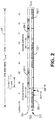
- Figure 2 illustrates one example of a TDD transmission frame 200 for use with system 100.
- Frame 200 comprises one or more downlink (DL) bursts 202 and one or more uplink (UL) bursts 204.
- DL downlink
- UL uplink
- DL downlink
- DL downlink
- UL uplink
- the structure of the TDD frame 200 is static for a given channel in system 100. That is, each TDD frame 200 for a given channel in system 100 has the same duration and the same number of downlink and uplink bursts having the same position and length within their respective frame 200.
- the example TDD frame 200 shown in Figure 2 is an example TDD LTE frame. Accordingly, the following discussion is specific to a TDD LTE frame. It should be understood, however, that other TDD frames can be used.
- the TDD frame 200 has a 10ms duration and includes 10 subframes having a 1ms duration.
- the TDD frame 200 includes two downlink bursts 202-1, 202-2 and two uplink bursts 204-1, 204-2.
- a first downlink burst 202-1 starts at the beginning of subframe #4 (4ms after the start of frame 200) and continues into subframe #6.
- a second downlink burst 202-2 starts at the beginning of subframe #9 (9ms after the start of frame 200), continues into the next frame 200, and ends within subframe #1 of the next frame 200.
- a first uplink burst 204-1 starts at the beginning of subframe #2 (2ms after the start of frame 200) and continues to the end of subframe #3).
- a second uplink burst 204-2 starts at the beginning of subframe #7 (7ms after the start of frame 200) and continues to the end of subframe #8).
- a "burst" is a portion of a TDD signal in which the TDD signal is continuous in the same direction.
- a downlink burst is a continuous downlink portion of the TDD signal and an uplink burst is a continuous uplink portion of the TDD signal.
- a continuous portion can have any structure, including one or more subframes as shown in Figure 2 .
- each (non-special) downlink subframe begins with a header/pilot time slot (DwPTS) followed by signal corresponding to payload data which extends to the end of the subframe.
- DwPTS header/pilot time slot
- the TDD signal over those multiple subframes will include a header or pilot time slot at the beginning of each subframe.
- the downlink signal will be continuous across the adjacent downlink subframes since the signal containing payload data of a first downlink subframe will extend until the header or pilot time slot of the subsequent downlink subframe.
- there is a signal present during all portions of a downlink subframe there is a signal present during all portions of a downlink subframe. Thus, a single burst can extend across a given subframe and across multiple adjacent downlink subframes.
- Special subframes start with a downlink header/pilot time slot followed by a guard period (GP) in which no downlink or uplink signals are transmitted.
- An uplink header/pilot time slot follows the guard period and extends to the end of the special subframe.
- signals are not continuous across the special subframe.
- downlink bursts 202 end in the special subframe and uplink bursts 204 begin in a special subframe.
- other frame structures can be used.
- the RF circuitry within DAS 103 switches between processing downlink signals and uplink signals in coordination with the downlink bursts 202 and uplink bursts 204.
- the RAUs 108-111 include such RF circuitry.
- the host unit 106 does not include any RF circuitry that switches with the downlink bursts 202 and uplink bursts 204. In other examples, however, the host unit 106 can also include switching RF circuitry.
- FIG. 3 is a block diagram of example RAU 108.
- RAU 108 includes one or more transport signal input/output ports 302 for sending and receiving transport signals with the host unit 106.
- the I/O ports 302 are optical ports for sending and receiving optical transport signals.
- the transport signals carry I/Q (complex) digital samples of a TDD signal.
- I/Q samples can be transported according to a serialized RF (SeRF) protocol used by ADC Telecommunications, Inc. (part of Commscope, Inc.) Shakopee, MN. In other embodiments, the I/Q samples can be transported using other transport protocols.
- SeRF serialized RF
- the first one or more processing devices 304 can be configured to generate uplink transport signals having uplink I/Q samples incorporated therein, and extract downlink I/Q samples from downlink transport signals.
- the uplink I/Q samples correspond to the uplink portion of a TDD signal and the downlink I/Q samples correspond to the downlink portion of the TDD signal.
- the first one or more processors 304 are discussed herein, it should be understood that addition components can be included on the SeRF board to implement the functionality described herein.
- the I/Q samples are communicated between the first one or more processing devices 304 and one or more RF system processors 308 over a radio system interface (RSI) 306.
- the one or more RF system processors 308 are configured to bi-directionally convert between I/Q samples and modulated analog signals for interaction with the transmitter(s) 310 and receiver(s) 312.
- the one or more RF system processors 308 are configured to digitally up-convert downlink I/Q samples to real digital IF samples and to digital to analog convert the IF samples to a modulated analog IF signal which is provided to the transmitter(s) 310.
- the one or more RF system processors 308 can also be configured to analog to digital convert an uplink modulated analog IF signal from the receiver(s) 312 to generate real digital IF samples and to digitally down-convert the IF samples into I/Q samples.
- the one or more RF system processors 308 can also be configured to recover the timing of the TDD signal as described below.
- the one or more RF system processors 308 can include a general purpose processor (GPP) or special purpose computer or processor (such as a field-programmable gate array (FPGA), application-specific integrated circuit (ASIC) or other integrated circuit), or any programmable logic device.
- the one or more RF system processors 308 are disposed on a second circuit board (motherboard).
- the transmitter(s) 310 can be configured to up-convert the downlink modulated analog IF signal to RF.
- the receiver(s) 312 can be configured to down-convert an uplink modulated analog RF signal to generate an uplink modulated analog IF signal for the one or more RF system processors 308.
- each transmitter 310 - receiver 312 pair 202 is implemented with a Digital/Analog Radio Transceiver (DART board) commercially available from ADC Telecommunications, Inc. (now part of Commscope, Inc.) of Shakopee, MN as part of the FlexWaveTM Prism line of products.
- DART board Digital/Analog Radio Transceiver
- Each DART board can be a separate circuit board from the motherboard that is configured to plug into a port (e.g., via an edge connector) of the motherboard.
- the DART board is also described in U.S. Patent Application Serial No. 11/627,251 , assigned to ADC Telecommunications, Inc., published in U.S. Patent Application Publication No. 2008/0181282 .
- the RAU 108 includes a downlink path and an uplink path.
- the downlink path includes a logical portion comprising the processing of the downlink digital samples (e.g., the I/Q and IF samples) and an analog portion comprising the generation of the RF modulated signal from the downlink digital samples.
- the uplink path includes an analog portion comprising the generation of an analog IF signal from a sensed RF signal at antenna(s) 104 and a logical portion comprising the processing of the IF signal to generate uplink digital samples (e.g., the I/Q and IF samples).
- the RAU 108 operates on multiple TDD RF signals concurrently (e.g., multiple bands), a downlink path and uplink path exists for each TDD RF signal.
- the RAU 108 has an uplink mode and downlink mode for each set of downlink and uplink paths.
- the uplink mode one or more of the components are set to enable operation on the uplink signals.
- the switching device 314 is set to couple RF signals from the antenna(s) 104 to the receiver 312, and the receiver 312 can be enabled.
- the uplink mode one or more of the components not used to process uplink signals can be disabled, such as the transmitter 310 and power amplifier 313.
- the downlink mode one or more of the components are set to enable operation on the downlink signals.
- switching device 314 is set to couple the RF signals from the transmitter 310 to the antenna(s) 104, and the transmitter 310 and power amplifier 313 are enabled. Additionally, in the downlink mode, one or more components not used to process downlink signals can be disabled, such as the receiver 312.
- Wireless terminals 112 obtain the timing of the downlink bursts 202 and uplink bursts 204 by decoding downlink signals sent by RAN node 102.
- the downlink signals include timing information indicating when each downlink burst 202 and uplink burst 204 begins and the duration of each.
- the DAS 103 does not demodulate and decode the signals transmitted between RAN node 102 and wireless terminals 112.
- DAS 103 independently determines the start time of the downlink bursts 202 and uplink bursts 204 in order to accurately switch between uplink mode and downlink mode.
- FIG. 4 is an example method 400 implemented by the DAS 103 to determine the start time of the downlink bursts 202 and uplink bursts 204 in a TDD frame 200.
- each RAU 108-111 implements method 400 to determine when to switch its RF circuitry.
- one or more "master" RAUs 108-111 implement the method 400 to determine the timing information, and communicate the timing information to the other RAUs 108-111.
- the host unit 106 implements the method 400 to determine the timing information and communicates the timing information to the RAUs 108-111.
- Method 400 is implemented by one or more processing devices.
- the one or more processing devices can include a general purpose processor (GPP) or special purpose computer or processor (such as a field-programmable gate array (FPGA), application-specific integrated circuit (ASIC) or other integrated circuit), or any programmable logic device.
- GPS general purpose processor
- FPGA field-programmable gate array
- ASIC application-specific integrated circuit
- Any of the processors described above may include or function with software programs, firmware or other computer readable instructions for carrying out various methods, process tasks, calculations, and control functions, used in the digital processing functionality described herein. These instructions are typically stored on any appropriate computer readable medium used for storage of computer readable instructions or data structures.
- Suitable processor-readable media may include storage or memory media such as magnetic or optical media.
- storage or memory media may include conventional hard disks, Compact Disk - Read Only Memory (CD-ROM), volatile or non-volatile media such as Random Access Memory (RAM) (including, but not limited to, Synchronous Dynamic Random Access Memory (SDRAM), Double Data Rate (DDR) RAM, RAMBUS Dynamic RAM (RDRAM), Static RAM (SRAM), etc.), Read Only Memory (ROM), Electrically Erasable Programmable ROM (EEPROM), and flash memory, etc.
- RAM Random Access Memory
- SDRAM Synchronous Dynamic Random Access Memory
- DDR Double Data Rate
- RDRAM RAMBUS Dynamic RAM
- SRAM Static RAM
- ROM Read Only Memory
- EEPROM Electrically Erasable Programmable ROM
- flash memory etc.
- Suitable processor-readable media may also include transmission media such as electrical, electromagnetic, or digital signals, conveyed via a communication medium such as a network and/or a wireless like.
- the one or more RF system processors 308 of the RAUs 108-111 can implement
- a processing device determines the start time of downlink bursts 202 and uplink bursts 204 by analyzing power samples of a downlink portion of a TDD signal.
- a RAU 108-111 includes a downlink path separate from an uplink path.
- the downlink path includes samples of the downlink portion of a TDD signal.
- the samples in the downlink path do not include the uplink portion of the TDD signal.
- the samples in the downlink path (ideally) include only noise.
- the samples in the downlink path are I/Q samples of the downlink portion of the TDD signal.
- the processing device can generate power samples (block 402) from the I/Q samples by squaring the I/Q samples.
- Power samples are samples in which the magnitude of the data therein corresponds to the magnitude of the power in the corresponding TDD signal.
- the processing device can take the appropriate steps, if any, to generate power samples therefrom.
- the processing device can then determine a power threshold (block 404) from the power samples.
- the power threshold is determined by grouping power samples into blocks, wherein each block corresponds to a respective time period of the downlink portion of the TDD signal (also referred to herein as "downlink TDD signal").
- each block is a contiguous time period, such that all time periods of the downlink TDD signal are captured in a respective block and there is no overlap of adjacent (in TDD signal time) blocks.
- each block corresponds to 10ms of TDD signal time, such that each block includes one frame's worth of power samples.
- each block corresponds to the minimum length of time of a downlink burst in the TDD signal.
- the minimum length of time can be set in any appropriate manner such as being based on the communication protocol or based on the known minimum length of the downlink burst in the given configuration.
- the minimum length of a downlink burst is 1ms, the length of subframe.
- the processing device can then generate a set of maximum power values, wherein each maximum power value is a representation of a maximum power level for a respective block.
- the maximum power value for a block can be represented in different manners.
- the power sample having the largest value is selected as the maximum power value for a respective block.
- the maximum power value can be an estimation of the power of the largest power symbol within the block. This estimation can be obtained by filtering the power samples for the block with a moving average filter having a time period corresponding to a length of a symbol in the TDD signal. This will generate a set of filtered values for the block.
- the largest filter value from the set can be selected as the maximum power value for the block.
- other manners of representing the maximum power level for a block can be used.
- an average power can be calculated from the set of maximum power levels.
- the power threshold can then be set based on the average power.
- the power threshold can be an a priori value that is manually input.
- the processing device compares the power samples of the downlink TDD signal to the power threshold in order to identify the start of a downlink burst. Since the downlink TDD signal does not include the power from the uplink portion of the TDD signal, the power level of the downlink TDD signal should increase substantially at the start of a downlink burst and maintain a power level above a noise floor until the end of the downlink burst. By comparing the power samples of the downlink TDD signal with the power threshold, the processing device can identify the start of a downlink burst in the downlink TDD signal.
- the power threshold In order to accurately identify the start of a downlink burst in the downlink TDD signal, the power threshold should be set above the noise floor of the downlink TDD signal and below a minimum (expected) power level of the downlink burst.
- the power threshold is set at a value of one of at least 10dB, at least 6dB, or at least 3dB less than the average power determined above. In an implementation of this example, the power threshold is set at a value of 30dB less than the average power.
- the noise floor of the downlink TDD signal during an uplink burst is estimated, and the power threshold is set at a value between the average power and the noise floor.
- the noise floor can be estimated by filtering the power samples of the downlink TDD signal with a moving average filter having a time period that is slightly less than the minimum length of an uplink burst in the TDD signal.
- the minimum length of an uplink burst can be set in any appropriate manner such as being based on the communication protocol or based on the known minimum length of the uplink burst in the given configuration. In the LTD TDD protocol, the minimum length of an uplink burst is 1ms, the length of subframe.
- the time period for the moving average filter is set at between 10 and 100 percent of the minimum length of an uplink burst.
- Filtering the power samples can produce a set of filtered values.
- set of filtered values includes values corresponding to the length of a frame 200 (e.g., 10ms). The minimum of the set of filtered values can be selected as the noise floor estimate for the downlink TDD signal.
- a noise variance of the downlink TDD signal during an uplink burst time period can be estimated.
- the noise variance can be estimated from the set of power samples that were used by the filter to generate the filtered value that was selected as the noise floor estimate.
- the noise variance can be used to calculate an offset from the estimated noise floor.
- the offset can be 2, 3, or 4 sigma with respect to the estimated noise floor.
- the power threshold can then be set at the noise floor plus the offset.
- the processing device can compare power samples of the downlink TDD signal to the power threshold to determine a start of a downlink burst.
- the power samples of the downlink TDD signal are grouped into blocks (block 406).
- each block corresponds to a respective time period of the downlink TDD signal.
- each block is a contiguous time period, such that all time periods of the downlink TDD signal are captured in a respective block and there is no overlap of adjacent (in TDD signal time) blocks.
- each block is less than 1/500 th the minimum length of a downlink burst in the TDD signal.
- each block includes at least 10 samples.
- each block corresponds to 260 nanoseconds of the downlink TDD signal.
- the power samples in each block are compared to the power threshold (block 408). Based on the comparison of the samples in each block to the power threshold, each block is assigned as ON or OFF (block 410). ON is used to represent a block in which a downlink signal is present and OFF is used to represent a block in which a downlink signal is not present. If a threshold number of samples in a given block are above the power threshold, the block is assigned as ON. Otherwise, the block is assigned as OFF. In an example, the threshold number of samples is 10 percent of the samples in a block. In an implementation of this example, the threshold number of samples is 1/6 th of the samples in a block.
- the processing device can then identify a start of a downlink burst by identifying an ON block preceded by at least a minimum number of consecutive OFF blocks (block 412). Since time periods corresponding to the uplink portion of the TDD signal in the downlink TDD signal are (ideally) only noise, the blocks corresponding to these uplink time periods should be assigned as OFF. Thus, the minimum number of OFF blocks used to identify a start of a downlink burst can correspond to the minimum length of an uplink burst in the TDD signal. As discussed above, in an LTE TDD example, this minimum length can be 1ms. Thus, once a number of consecutive OFF blocks corresponding to 1ms of time are identified, the next ON block is identified as the start of a downlink burst. In this way, the start of a downlink burst can be identified by the DAS 103 based on samples of the downlink TDD signal, without demodulating and decoding the TDD signal.
- the DAS 103 can use the start to switch one or more components between downlink mode and uplink mode. For example, the duration of each downlink burst as well as the relative start times of subsequent bursts 202, 204 with the frame 200 can be input (e.g., manually) into the DAS 103 and used to calculate the start and end of each burst 202, 204 based on the identified start of one of the downlink bursts. In examples, where multiple downlink bursts 202 are included in a frame 200, the start of each of the downlink bursts 202 may need to be identified to remove ambiguity between the downlink bursts 202.
- the end of the downlink burst 202 can be determined by the one or more processing devices, for example, by identifying an OFF block following one or more ON blocks. Additionally, in some examples, a similar method to method 400 can be performed on uplink samples in the uplink path to identify a start and/or end of an uplink burst 204.
- the end of the downlink burst(s) 202 and the start and end of the uplink burst(s) 204 can be determined.
- the start and end of the respective downlink burst(s) 202 and uplink burst(s) 204 can be used to set one or more components (e.g., RAU 108, switching device 314, etc.) into downlink or uplink mode respectively.
- specifically timed uplink and/or downlink mode switching schemes can be used which, for example, switch/enable/disable some components prior to other components.
- the power amplifier 313 in the downlink path may be disabled prior to setting the switching device 314 into uplink mode to reduce the likelihood of high power signals being coupled into the uplink path.
- the above process of identifying the start of a downlink burst 202 can be implemented one or a couple times during a training mode of the DAS 103/RAU 108-111 to initially find and lock onto the start of a downlink burst 202. Once locked onto the start of a downlink burst 202, the above process can end and the DAS 103/RAU 108-111 can predict the start of subsequent bursts 202/204 based on the identified start of a downlink burst 202. In such an example, other schemes can be used to maintain the burst timing.
- the above process of identifying the start of a downlink burst 202 can be repeated continually during steady state operation with a continually updated set of blocks (updated to correspond to a more current time) to continually identify the start of a downlink burst 202 and control the one or more components accordingly.
- the above process can be used to maintain the burst timing.
- the processing device can predict the start of a downlink burst 202 based on the start of one or more previous downlink bursts 202.
- the prediction can be based on relative timing of subsequent downlink bursts 202 (e.g., the length of time between starts of downlink bursts 202) which can, for example, be input manually.
- the processing device can identify/observe the start of the subsequent downlink burst using the process described above.
- the process device can set an adjusted start of the subsequent downlink burst 202 at a time between the predicted start and the identified start.
- the adjusted start of the subsequent downlink burst 202 can then be used to control the one or more components and/or for a subsequent prediction of a later downlink burst 202.
- the adjusted start can be set at a second offset from the predicted start.
- the second offset can be selected to adjust the error in the predicted start (difference between predicted start and identified start) over multiple iterations/adjustments to reduce jitter in the adjusted start value. That is, an error of the predicted start is only partially accounted for in a given adjustment. If a subsequent determination for a subsequent downlink burst 202 indicates a further error, the error is adjusted further at that time. This iterative process continues to gradually adjust for error over multiple iterations.
- the second offset can be a fixed small increment of time (e.g., 1 microsecond).
- the second offset can be a fixed percentage of the difference between the predicted start and the identified start (e.g., 25%). In any case, tempering the adjustment of the start in this manner can reduce jitter in the adjustment, while allowing full correction of the error over multiple adjustments.
- the adjusted start can be set based on integrating the difference (error) between the predicted start and the identified start over time. Other manners of accounting for the error can also be used.
- Subsequent predicted starts for subsequent downlink bursts 202 can be determined based on the adjusted, predicted, and/or identified starts of one or more previous downlink bursts 202.
- the predicted start for a given downlink bursts 202 can be based on an averaging of an adjusted start of multiple previous downlink bursts 202 while taking into account a length of time (e.g., that is manually input) between starts of downlink bursts 202.
- the process of predicting the start, identifying the start, and setting an adjusted start can be implemented during steady state operation, and a different process can be implemented during a training phase. For example, during the training phase, larger adjustments to the predicted start can be allowed.
- the processing device can determine when to transition out of the training phase and to steady state operation based on a threshold number of successful predicted starts, that is, a threshold number of predicted starts that are sufficiently close to the corresponding identified start. In some examples, the processing device can also determine when to transition out of steady state operation and back into the training phase based on a threshold number of predicted start being sufficiently far from the corresponding identified start. In an implementation of this example, 15 consecutive successful predicted starts can be used at the threshold to determine when to transition from the training phase to steady state operation and 4 consecutive predicted starts being sufficiently far from the identified start can be used as the threshold to determine when to transition from steady state operation to the training phase.
- this process of predicting the start, identifying the start, and setting an adjusted start of a downlink burst 202 can be repeated continually to maintain the TDD timing over time.
- the process of predicting, identifying, and adjusting can be performed for all downlink bursts 202 of the TDD signal.
- the process of predicting, identifying, and adjusting can be performed for less than all (e.g., one per frame 200, one per 10 frames, etc.) of the downlink bursts 202 of the TDD signal.
- Continually identifying the start of downlink bursts 202 can include continually setting the power threshold based on a continually updated set of blocks (updated to correspond to a more current time) to continually adjust the power threshold based on the updated power samples of the TDD signal.
- the power threshold can be static after an initial training phase.
- the downlink samples can be filtered to extract one or more specific frequencies from which the timing can be obtained. Such filtering could be used, for example, to extract a reference signal from the downlink TDD signal.
Landscapes
- Engineering & Computer Science (AREA)
- Signal Processing (AREA)
- Computer Networks & Wireless Communication (AREA)
- Mobile Radio Communication Systems (AREA)
Claims (15)
- Procédé (400) pour déterminer le cadencement d'un signal en duplex par répartition dans le temps, TDD, dans un système d'antennes distribuées, DAS, le procédé comprenant les étapes consistant à :regrouper (406) des échantillons de puissance d'une partie de liaison descendante du signal TDD en blocs correspondant à une période de temps respective ;comparer (408) des échantillons de puissance des blocs à un seuil de puissance ;définir (410) les blocs comme des blocs ON ou OFF sur la base d'un nombre d'échantillons de puissance dans un bloc respectif qui sont au-dessus du seuil de puissance ;identifier (412) un début d'une salve de liaison descendante dans le signal TDD comme un bloc ON précédé d'au moins un nombre minimal de blocs OFF consécutifs ; etcommander au moins un composant du DAS sur la base du début de la salve de liaison descendante.
- Procédé (400) selon la revendication 1, dans lequel chaque bloc correspond à une durée commune et, éventuellement,
dans lequel la durée commune est inférieure à 1/500ème d'une durée minimale d'une salve de liaison descendante dans le signal TDD, dans lequel la durée commune correspond à au moins 10 échantillons, dans lequel chaque bloc correspond à une période de temps contiguë. - Procédé (400) selon l'une quelconque des revendications 1 à 2, comprenant l'étape consistant à :
générer les échantillons de puissance par élévation au carré d'échantillons de données complexes. - Procédé (400) selon l'une quelconque des revendications 1 à 3, dans lequel définir les blocs comme des blocs ON ou OFF consiste à définir le bloc respectif comme bloc ON si plus d'un nombre minimal d'échantillons de puissance dans le bloc respectif sont au-dessus du seuil de puissance, et, éventuellement,
dans lequel le nombre minimal d'échantillons de puissance est d'au moins 10 pour cent des échantillons de puissance dans le bloc respectif. - Procédé (400) selon l'une quelconque des revendications 1 à 4, dans lequel le nombre minimal de blocs OFF consécutifs est inférieur ou égal à un nombre de blocs correspondant à la longueur minimale d'une salve de liaison montante dans le signal TDD.
- Procédé (400) selon l'une quelconque des revendications 1 à 5, comprenant l'étape consistant à :
ajuster en continu le seuil de puissance sur la base d'échantillons de puissance du signal TDD. - Procédé (400) selon la revendication 6, dans lequel ajuster en continu le seuil de puissance consiste à :regrouper des échantillons de puissance de la partie de liaison descendante du signal TDD en seconds blocs correspondant à une période de temps respective ;générer un ensemble de valeurs de puissance maximale, l'ensemble de valeurs de puissance maximale consistant en une valeur de puissance maximale pour chacun d'un ensemble contigu des seconds blocs ;calculer une puissance moyenne de l'ensemble de valeurs de puissance maximale ; etrégler le seuil de puissance sur la base de la puissance moyenne.
- Procédé (400) selon la revendication 7, dans lequel générer l'ensemble de valeurs de puissance maximale consiste à :
sélectionner le plus grand échantillon de puissance de chacun des seconds blocs dans l'ensemble contigu comme valeur de puissance maximale pour ce second bloc. - Procédé (400) selon la revendication 7, dans lequel générer l'ensemble de valeurs de puissance maximale consiste, pour chacun des seconds blocs dans l'ensemble contigu, à :filtrer les échantillons de puissance pour un bloc respectif avec un filtre à moyenne mobile ayant une période de temps correspondant à une longueur d'un symbole du signal TDD pour générer un ensemble de valeurs filtrées pour le bloc respectif ; etsélectionner la plus grande valeur filtrée pour le bloc respectif comme valeur de puissance maximale pour le bloc respectif.
- Procédé (400) selon la revendication 7, dans lequel regrouper les échantillons de puissance consiste à regrouper les échantillons de puissance en blocs ayant une durée commune qui est au moins la durée minimale d'une salve de liaison descendante dans le signal TDD, et, éventuellement,
dans lequel régler le seuil de puissance consiste à régler le seuil de puissance à une valeur inférieure d'au moins 3 dB à la puissance moyenne. - Procédé (400) selon la revendication 7, comprenant les étapes consistant à :estimer un plancher de bruit de la partie de liaison descendante du signal TDD pendant une période de temps de salve de liaison montante,dans lequel régler le seuil de puissance consiste à régler le seuil de puissance à une valeur v comprise entre la puissance moyenne et le plancher de bruit, et, éventuellement,dans lequel estimer le plancher de bruit consiste à :filtrer des échantillons de puissance de la partie de liaison descendante du signal TDD avec un filtre à moyenne mobile ayant une période de temps qui est comprise entre 10 et 100 pour cent de la longueur minimale d'une salve de liaison montante dans le signal TDD pour générer une pluralité de secondes puissances moyennes ; etsélectionner le minimum de la pluralité de secondes puissances moyennes comme plancher de bruit ;le procédé comprenant en outre les étapes consistant à :estimer une variance de bruit de la partie de liaison descendante du signal TDD pendant la période de temps de salve de liaison montante ; etcalculer un décalage sur la base de la variance de bruit,dans lequel régler le seuil de puissance consiste à régler le seuil de puissance au plancher de bruit plus le décalage.
- Procédé (400) selon l'une quelconque des revendications 1 à 11, comprenant les étapes consistant à :déterminer le nombre de blocs ON consécutifs à partir du début de la salve de liaison descendante ; etsi le nombre de blocs ON consécutifs n'est pas égal à une durée prévue de la salve de liaison descendante, régler une alarme.
- Procédé (400) selon l'une quelconque des revendications 1 à 12, dans lequel commander au moins un composant consiste à :régler un commutateur pour passer du couplage d'une voie de liaison descendante à une ou plusieurs antennes au couplage d'une voie de liaison montante auxdites une ou plusieurs antennes ; etdésactiver un amplificateur de puissance dans la voie de liaison descendante avant de régler le commutateur pour coupler une voie de liaison montante auxdites une ou plusieurs antennes, et, éventuellement,le procédé comprenant en outre les étapes consistant à :identifier en continu un début de salves de liaison descendante suivantes respectives dans le signal TDD en identifiant un bloc ON précédé d'au moins un nombre minimal de blocs OFF consécutifs ; etcommander au moins un composant dans le DAS sur la base du début des salves de liaison descendante suivantes respectives.
- Procédé (400) selon l'une quelconque des revendications 1 à 13, comprenant les étapes consistant à :prédire un début de la salve de liaison descendante sur la base d'un début d'une ou plusieurs salves de liaison descendante précédentes ;si le début identifié de la salve de liaison descendante est différent du début prédit de la salve de liaison descendante, régler un début ajusté pour la salve de liaison descendante à un moment entre le début prédit et le début identifié ; etdans lequel commander au moins un composant dans le DAS consiste à commuter ledit au moins un composant sur la base du début ajusté, et, éventuellement,le procédé comprenant en outre les étapes consistant à :prédire en continu un début de salves de liaison descendante suivantes respectives dans le signal TDD sur la base d'un début ajusté d'une ou plusieurs salves de liaison descendante précédentes ;identifier en continu un début des salves de liaison descendante suivantes respectives en identifiant un bloc ON précédé d'au moins un nombre minimal de blocs OFF consécutifs ;régler en continu un début ajusté pour les salves de liaison descendante suivantes respectives à un moment situé entre le début prévu et le début identifié pour la salve de liaison descendante suivante respective si le début identifié pour la salve de liaison descendante suivante respective est différent du début prévu pour la salve de liaison descendante suivante respective ; etcommander au moins un composant dans le DAS sur la base du début ajusté des salves de liaison descendante suivantes respectives,dans lequel régler en continu un début ajusté inclut l'une des opérations consistant à :régler les débuts ajustés à un ajustement commun à partir de leur début prédit respectif si la différence entre leur début identifié respectif et leur début prédit respectif est supérieure à l'ajustement ; etrégler les débuts ajustés à un second ajustement à partir de leur début prédit respectif, dans lequel le second ajustement est un pourcentage réglé de la différence entre leur début prédit respectif et leur début identifié respectif, dans lequel le pourcentage réglé est le même pour chaque différence qui est supérieure à un seuil.
- Unité distante (108, 109, 110, 111) pour un système d'antennes distribuées (103), l'unité distante (108, 109, 110, 111) comprenant :une ou plusieurs antennes (104) pour émettre des signaux de liaison descendante et pour détecter des signaux de liaison montante ;un commutateur (314) configuré pour coupler sélectivement une voie de communication de liaison descendante ou une voie de communication de liaison montante auxdites une ou plusieurs antennes ;un ou plusieurs dispositifs de traitement (308), dans lequel lesdits un ou plusieurs dispositifs de traitement (308) sont configurés pour mettre en oeuvre le procédé selon l'une quelconque des revendications 1 à 14.
Priority Applications (1)
| Application Number | Priority Date | Filing Date | Title |
|---|---|---|---|
| EP20191953.7A EP3761525B1 (fr) | 2015-10-03 | 2016-10-03 | Récupération de synchronisation tdd dans un système d'antenne réparti |
Applications Claiming Priority (2)
| Application Number | Priority Date | Filing Date | Title |
|---|---|---|---|
| US201562236870P | 2015-10-03 | 2015-10-03 | |
| PCT/US2016/055184 WO2017059435A1 (fr) | 2015-10-03 | 2016-10-03 | Récupération de synchronisation tdd dans un système d'antenne réparti |
Related Child Applications (1)
| Application Number | Title | Priority Date | Filing Date |
|---|---|---|---|
| EP20191953.7A Division EP3761525B1 (fr) | 2015-10-03 | 2016-10-03 | Récupération de synchronisation tdd dans un système d'antenne réparti |
Publications (3)
| Publication Number | Publication Date |
|---|---|
| EP3357166A1 EP3357166A1 (fr) | 2018-08-08 |
| EP3357166A4 EP3357166A4 (fr) | 2019-05-29 |
| EP3357166B1 true EP3357166B1 (fr) | 2020-09-02 |
Family
ID=58427959
Family Applications (2)
| Application Number | Title | Priority Date | Filing Date |
|---|---|---|---|
| EP16852831.3A Active EP3357166B1 (fr) | 2015-10-03 | 2016-10-03 | Récupération de synchronisation tdd dans un système d'antenne réparti |
| EP20191953.7A Active EP3761525B1 (fr) | 2015-10-03 | 2016-10-03 | Récupération de synchronisation tdd dans un système d'antenne réparti |
Family Applications After (1)
| Application Number | Title | Priority Date | Filing Date |
|---|---|---|---|
| EP20191953.7A Active EP3761525B1 (fr) | 2015-10-03 | 2016-10-03 | Récupération de synchronisation tdd dans un système d'antenne réparti |
Country Status (4)
| Country | Link |
|---|---|
| US (1) | US10673604B2 (fr) |
| EP (2) | EP3357166B1 (fr) |
| CN (1) | CN108352854B (fr) |
| WO (1) | WO2017059435A1 (fr) |
Families Citing this family (11)
| Publication number | Priority date | Publication date | Assignee | Title |
|---|---|---|---|---|
| US20190342014A1 (en) * | 2016-07-01 | 2019-11-07 | Telefonaktiebolaget Lm Ericsson (Publ) | Over the air testing of a radio communications device |
| US10454571B2 (en) * | 2017-07-20 | 2019-10-22 | Corning Optical Communications LLC | Dynamic determination of threshold power level for use in distinguishing between downlink and uplink periods in time-division duplexed (TDD) communications |
| US20210029564A1 (en) * | 2018-05-17 | 2021-01-28 | Andrew Wireless Systems Gmbh | User equipment assisted leveling and optimization of distributed antenna systems |
| CN109361416B (zh) * | 2018-10-31 | 2020-07-28 | 深圳昂瑞微电子技术有限公司 | 一种符号定时恢复电路及其接收机 |
| US10616005B1 (en) * | 2018-11-28 | 2020-04-07 | Samsung Electronics Co., Ltd. | Robust noise power estimation |
| WO2021050866A1 (fr) | 2019-09-13 | 2021-03-18 | Commscope Technologies Llc | Système répéteur destiné à être utilisé avec une nouvelle station de base radio 5g qui utilise un duplexage par répartition dans le temps |
| US11956185B2 (en) | 2020-04-15 | 2024-04-09 | Corning Research & Development Corporation | Time-division duplexing (TDD) detection in wireless distributed communications systems (DCS) to synchronize TDD downlink and uplink communications, and related methods |
| US11503554B2 (en) * | 2020-05-13 | 2022-11-15 | Sprint Spectrum L.P. | Dynamically accounting for past transmit power as basis to set future transmit power on co-existing air interface |
| US12069006B2 (en) | 2021-06-18 | 2024-08-20 | Corning Research & Development Corporation | Systems and methods for time division duplex (TDD) synchronizing in distributed communication systems (DCSs) |
| US12432614B2 (en) * | 2022-06-09 | 2025-09-30 | Outdoor Wireless Networks LLC | Techniques about converting time-domain fronthaul data to frequency-domain fronthaul data within a distributed antenna system |
| WO2023241805A1 (fr) * | 2022-06-16 | 2023-12-21 | Telefonaktiebolaget Lm Ericsson (Publ) | Procédé et appareil de détermination de niveau de puissance par analyse d'une occurrence de valeurs d'échantillons de puissance reçus pendant un intervalle de temps |
Family Cites Families (24)
| Publication number | Priority date | Publication date | Assignee | Title |
|---|---|---|---|---|
| CN1993904B (zh) | 2004-05-13 | 2011-09-07 | 高通股份有限公司 | 具有用于上行链路及下行链路同步之下行链路检测的非变频中继器 |
| US20070268846A1 (en) | 2006-03-31 | 2007-11-22 | Widefi, Inc. | Enhanced physical layer repeater for operation in WiMAX systems |
| WO2008076248A1 (fr) * | 2006-12-13 | 2008-06-26 | Powerwave Technologies, Inc. | Générateur de signal de transition d'avant en arrière duplex à répartition dans le temps |
| US8737454B2 (en) | 2007-01-25 | 2014-05-27 | Adc Telecommunications, Inc. | Modular wireless communications platform |
| US8437792B2 (en) * | 2007-02-14 | 2013-05-07 | Qualcomm Incorporated | Uplink power control for LTE |
| US8165100B2 (en) | 2007-12-21 | 2012-04-24 | Powerwave Technologies, Inc. | Time division duplexed digital distributed antenna system |
| DE102008017881B9 (de) | 2008-04-09 | 2012-11-08 | Andrew Wireless Systems Gmbh | TDD-Repeater für ein Drahtlos-Netz und Verfahren zum Betrieb eines solchen Repeaters |
| US8310963B2 (en) | 2008-06-24 | 2012-11-13 | Adc Telecommunications, Inc. | System and method for synchronized time-division duplex signal switching |
| US8626238B2 (en) * | 2008-06-24 | 2014-01-07 | Adc Telecommunications, Inc. | Method and apparatus for switching in a TDD system |
| US8208414B2 (en) | 2008-06-24 | 2012-06-26 | Lgc Wireless, Inc. | System and method for configurable time-division duplex interface |
| US8385373B2 (en) | 2008-06-24 | 2013-02-26 | Adc Telecommunications, Inc. | Method and apparatus for frame detection in a communications system |
| US7961689B2 (en) | 2008-08-18 | 2011-06-14 | Adc Telecommunications, Inc. | Method and apparatus for determining an end of a subframe in a TDD system |
| EP2180605B1 (fr) | 2008-10-27 | 2013-01-09 | Andrew Wireless Systems GmbH | Répétiteur et procédé d'utilisation d'un tel répétiteur |
| US8050246B2 (en) | 2009-03-03 | 2011-11-01 | Adc Telecommunications, Inc. | Range extension for time division duplex systems |
| KR101508978B1 (ko) * | 2009-04-20 | 2015-04-07 | 주식회사 케이엠더블유 | Tdd용 기지국 안테나의 송수신 타이밍 제어 방법 및 상기 방법이 적용된 기지국 안테나 |
| CN103210598B (zh) * | 2010-08-13 | 2017-03-22 | 爱立信(中国)通信有限公司 | 基站中用于时分双工无线通信的自动保护期调整 |
| CN102404761B (zh) * | 2010-09-15 | 2014-02-05 | 联芯科技有限公司 | Td同步定时保持及基于其进行异系统测量的方法与装置 |
| US9172344B2 (en) * | 2011-03-24 | 2015-10-27 | Silicon Laboratories Inc. | Statistical gain control in a receiver |
| US8693342B2 (en) | 2011-10-28 | 2014-04-08 | Adc Telecommunications, Inc. | Distributed antenna system using time division duplexing scheme |
| WO2014199380A1 (fr) * | 2013-06-12 | 2014-12-18 | Corning Optical Communications Wireless, Ltd. | Duplexage par répartition temporelle (tdd) dans des systèmes de communication répartis, comprenant des systèmes d'antenne répartis (das) |
| EP3039943A1 (fr) | 2013-08-29 | 2016-07-06 | Corning Optical Communications Wireless Ltd. | Détection de configurations de trames à duplexage par répartition dans le temps (tdd) en liaison montante/descendante pour synchroniser des communications en liaison montante et descendante tdd entre des équipements de communication tdd |
| CN110071791B (zh) * | 2013-10-30 | 2022-04-19 | 安德鲁无线系统有限公司 | 用于利用时分双工的分布式天线系统的切换子系统 |
| EP3737004B1 (fr) * | 2014-04-11 | 2022-01-12 | CommScope Technologies LLC | Duplexage par répartition en fréquence dans un mode de duplexage par répartition dans le temps pour un système de télécommunications |
| CA2976822C (fr) * | 2015-02-20 | 2019-07-16 | Telefonaktiebolaget Lm Ericsson (Publ) | Unite radio et procede correspondant pour le reglage de niveaux de puissance d'emetteurs-recepteurs separes dans l'espace dans un reseau de communication sans fil |
-
2016
- 2016-10-03 EP EP16852831.3A patent/EP3357166B1/fr active Active
- 2016-10-03 WO PCT/US2016/055184 patent/WO2017059435A1/fr not_active Ceased
- 2016-10-03 CN CN201680066654.1A patent/CN108352854B/zh not_active Expired - Fee Related
- 2016-10-03 US US15/765,712 patent/US10673604B2/en active Active
- 2016-10-03 EP EP20191953.7A patent/EP3761525B1/fr active Active
Non-Patent Citations (1)
| Title |
|---|
| None * |
Also Published As
| Publication number | Publication date |
|---|---|
| EP3761525A1 (fr) | 2021-01-06 |
| US20180302210A1 (en) | 2018-10-18 |
| CN108352854A (zh) | 2018-07-31 |
| WO2017059435A1 (fr) | 2017-04-06 |
| EP3357166A1 (fr) | 2018-08-08 |
| CN108352854B (zh) | 2020-09-04 |
| EP3761525B1 (fr) | 2023-01-04 |
| US10673604B2 (en) | 2020-06-02 |
| EP3357166A4 (fr) | 2019-05-29 |
Similar Documents
| Publication | Publication Date | Title |
|---|---|---|
| EP3357166B1 (fr) | Récupération de synchronisation tdd dans un système d'antenne réparti | |
| CN112640543B (zh) | 新无线电中的定时提前 | |
| EP2319203B1 (fr) | Procédé et appareil permettant de déterminer une fin d'une sous-trame dans un système tdd | |
| US9602270B2 (en) | Clock drift compensation in a time synchronous channel hopping network | |
| US11563481B2 (en) | Method and apparatus for relay based on multiple beams in vehicle-to-everything communication system | |
| US10187239B2 (en) | Systems and methods to reduce the peak-to-average power ratio (PAPR) of signals in channel bonding | |
| EP3349407B1 (fr) | Procédé permettant de supprimer l'auto-brouillage d'un appareil utilisant un système fdr | |
| EP4297327A2 (fr) | Configuration de ressources d'atténuation d'interférences à distance | |
| US10652955B2 (en) | DAS management by radio access network node | |
| WO2015078483A1 (fr) | Procédé et appareil pour combiner des transmissions bidirectionnelles à l'alternat et simultanée dans un relais | |
| EP4527008A1 (fr) | Commande automatique de gain pour modulations d'ordre supérieur | |
| US11528671B2 (en) | Frame structure to support long distance transmission | |
| CN101594705B (zh) | 时分双工系统的定时调整方法及基站 | |
| EP3254421B1 (fr) | Systèmes et procédés pour émuler des signaux de diversité de liaison montante | |
| CN109923908B (zh) | 修改的多间隙扩展覆盖随机接入信道传输 | |
| US20240406033A1 (en) | Methods for enabling and handling joint channel estimation and related devices | |
| WO2025213847A1 (fr) | Ltm conditionnel ultérieur et rétablissement de pdcp | |
| WO2025033516A1 (fr) | Dispositif et procédé de commande, station de relais | |
| WO2025033519A1 (fr) | Dispositif de commande, station de relais et procédé de commande | |
| CN119072952A (zh) | 用于确定各种转发链路的定时的系统和方法 | |
| CN120883537A (zh) | 用于可重新配置智能表面的反馈信令增强 | |
| CN119586029A (zh) | 中继器回传链路的波束指示 | |
| CN117223245A (zh) | 用于确定由无线设备转发的信号的特性的技术 | |
| CN121153310A (zh) | 非线性功率放大器操作模式指示 | |
| CN119586283A (zh) | 用于无线网络中的波束指示的方法和系统 |
Legal Events
| Date | Code | Title | Description |
|---|---|---|---|
| STAA | Information on the status of an ep patent application or granted ep patent |
Free format text: STATUS: THE INTERNATIONAL PUBLICATION HAS BEEN MADE |
|
| PUAI | Public reference made under article 153(3) epc to a published international application that has entered the european phase |
Free format text: ORIGINAL CODE: 0009012 |
|
| STAA | Information on the status of an ep patent application or granted ep patent |
Free format text: STATUS: REQUEST FOR EXAMINATION WAS MADE |
|
| 17P | Request for examination filed |
Effective date: 20180412 |
|
| AK | Designated contracting states |
Kind code of ref document: A1 Designated state(s): AL AT BE BG CH CY CZ DE DK EE ES FI FR GB GR HR HU IE IS IT LI LT LU LV MC MK MT NL NO PL PT RO RS SE SI SK SM TR |
|
| AX | Request for extension of the european patent |
Extension state: BA ME |
|
| DAV | Request for validation of the european patent (deleted) | ||
| DAX | Request for extension of the european patent (deleted) | ||
| A4 | Supplementary search report drawn up and despatched |
Effective date: 20190429 |
|
| RIC1 | Information provided on ipc code assigned before grant |
Ipc: H04B 1/54 20060101AFI20190423BHEP Ipc: H04B 1/44 20060101ALI20190423BHEP Ipc: H04B 7/26 20060101ALI20190423BHEP |
|
| GRAP | Despatch of communication of intention to grant a patent |
Free format text: ORIGINAL CODE: EPIDOSNIGR1 |
|
| STAA | Information on the status of an ep patent application or granted ep patent |
Free format text: STATUS: GRANT OF PATENT IS INTENDED |
|
| INTG | Intention to grant announced |
Effective date: 20200326 |
|
| GRAS | Grant fee paid |
Free format text: ORIGINAL CODE: EPIDOSNIGR3 |
|
| GRAA | (expected) grant |
Free format text: ORIGINAL CODE: 0009210 |
|
| STAA | Information on the status of an ep patent application or granted ep patent |
Free format text: STATUS: THE PATENT HAS BEEN GRANTED |
|
| AK | Designated contracting states |
Kind code of ref document: B1 Designated state(s): AL AT BE BG CH CY CZ DE DK EE ES FI FR GB GR HR HU IE IS IT LI LT LU LV MC MK MT NL NO PL PT RO RS SE SI SK SM TR |
|
| REG | Reference to a national code |
Ref country code: GB Ref legal event code: FG4D |
|
| REG | Reference to a national code |
Ref country code: AT Ref legal event code: REF Ref document number: 1309999 Country of ref document: AT Kind code of ref document: T Effective date: 20200915 Ref country code: CH Ref legal event code: EP |
|
| REG | Reference to a national code |
Ref country code: DE Ref legal event code: R096 Ref document number: 602016043445 Country of ref document: DE |
|
| REG | Reference to a national code |
Ref country code: IE Ref legal event code: FG4D |
|
| REG | Reference to a national code |
Ref country code: NL Ref legal event code: FP |
|
| RAP2 | Party data changed (patent owner data changed or rights of a patent transferred) |
Owner name: COMMSCOPE TECHNOLOGIES LLC |
|
| RIN2 | Information on inventor provided after grant (corrected) |
Inventor name: HEDIN, JOHN M. Inventor name: STRATFORD, SCOTT |
|
| REG | Reference to a national code |
Ref country code: DE Ref legal event code: R081 Ref document number: 602016043445 Country of ref document: DE Owner name: OUTDOOR WIRELESS NETWORKS LLC (N.D.GES.D.STAAT, US Free format text: FORMER OWNER: ADC TELECOMMUNICATIONS, INC., SHAKOPEE, MINN., US Ref country code: DE Ref legal event code: R082 Ref document number: 602016043445 Country of ref document: DE Representative=s name: MURGITROYD & COMPANY, DE Ref country code: DE Ref legal event code: R081 Ref document number: 602016043445 Country of ref document: DE Owner name: COMMSCOPE TECHNOLOGIES LLC, HICKORY, US Free format text: FORMER OWNER: ADC TELECOMMUNICATIONS, INC., SHAKOPEE, MINN., US |
|
| REG | Reference to a national code |
Ref country code: LT Ref legal event code: MG4D |
|
| PG25 | Lapsed in a contracting state [announced via postgrant information from national office to epo] |
Ref country code: SE Free format text: LAPSE BECAUSE OF FAILURE TO SUBMIT A TRANSLATION OF THE DESCRIPTION OR TO PAY THE FEE WITHIN THE PRESCRIBED TIME-LIMIT Effective date: 20200902 Ref country code: BG Free format text: LAPSE BECAUSE OF FAILURE TO SUBMIT A TRANSLATION OF THE DESCRIPTION OR TO PAY THE FEE WITHIN THE PRESCRIBED TIME-LIMIT Effective date: 20201202 Ref country code: GR Free format text: LAPSE BECAUSE OF FAILURE TO SUBMIT A TRANSLATION OF THE DESCRIPTION OR TO PAY THE FEE WITHIN THE PRESCRIBED TIME-LIMIT Effective date: 20201203 Ref country code: LT Free format text: LAPSE BECAUSE OF FAILURE TO SUBMIT A TRANSLATION OF THE DESCRIPTION OR TO PAY THE FEE WITHIN THE PRESCRIBED TIME-LIMIT Effective date: 20200902 Ref country code: NO Free format text: LAPSE BECAUSE OF FAILURE TO SUBMIT A TRANSLATION OF THE DESCRIPTION OR TO PAY THE FEE WITHIN THE PRESCRIBED TIME-LIMIT Effective date: 20201202 Ref country code: FI Free format text: LAPSE BECAUSE OF FAILURE TO SUBMIT A TRANSLATION OF THE DESCRIPTION OR TO PAY THE FEE WITHIN THE PRESCRIBED TIME-LIMIT Effective date: 20200902 Ref country code: HR Free format text: LAPSE BECAUSE OF FAILURE TO SUBMIT A TRANSLATION OF THE DESCRIPTION OR TO PAY THE FEE WITHIN THE PRESCRIBED TIME-LIMIT Effective date: 20200902 |
|
| REG | Reference to a national code |
Ref country code: AT Ref legal event code: MK05 Ref document number: 1309999 Country of ref document: AT Kind code of ref document: T Effective date: 20200902 |
|
| REG | Reference to a national code |
Ref country code: NL Ref legal event code: PD Owner name: COMMSCOPE TECHNOLOGIES LLC; US Free format text: DETAILS ASSIGNMENT: CHANGE OF OWNER(S), ASSIGNMENT; FORMER OWNER NAME: ADC TELECOMMUNICATIONS INC. Effective date: 20210210 |
|
| PG25 | Lapsed in a contracting state [announced via postgrant information from national office to epo] |
Ref country code: RS Free format text: LAPSE BECAUSE OF FAILURE TO SUBMIT A TRANSLATION OF THE DESCRIPTION OR TO PAY THE FEE WITHIN THE PRESCRIBED TIME-LIMIT Effective date: 20200902 Ref country code: PL Free format text: LAPSE BECAUSE OF FAILURE TO SUBMIT A TRANSLATION OF THE DESCRIPTION OR TO PAY THE FEE WITHIN THE PRESCRIBED TIME-LIMIT Effective date: 20200902 Ref country code: LV Free format text: LAPSE BECAUSE OF FAILURE TO SUBMIT A TRANSLATION OF THE DESCRIPTION OR TO PAY THE FEE WITHIN THE PRESCRIBED TIME-LIMIT Effective date: 20200902 |
|
| PG25 | Lapsed in a contracting state [announced via postgrant information from national office to epo] |
Ref country code: RO Free format text: LAPSE BECAUSE OF FAILURE TO SUBMIT A TRANSLATION OF THE DESCRIPTION OR TO PAY THE FEE WITHIN THE PRESCRIBED TIME-LIMIT Effective date: 20200902 Ref country code: PT Free format text: LAPSE BECAUSE OF FAILURE TO SUBMIT A TRANSLATION OF THE DESCRIPTION OR TO PAY THE FEE WITHIN THE PRESCRIBED TIME-LIMIT Effective date: 20210104 Ref country code: CZ Free format text: LAPSE BECAUSE OF FAILURE TO SUBMIT A TRANSLATION OF THE DESCRIPTION OR TO PAY THE FEE WITHIN THE PRESCRIBED TIME-LIMIT Effective date: 20200902 Ref country code: EE Free format text: LAPSE BECAUSE OF FAILURE TO SUBMIT A TRANSLATION OF THE DESCRIPTION OR TO PAY THE FEE WITHIN THE PRESCRIBED TIME-LIMIT Effective date: 20200902 Ref country code: SM Free format text: LAPSE BECAUSE OF FAILURE TO SUBMIT A TRANSLATION OF THE DESCRIPTION OR TO PAY THE FEE WITHIN THE PRESCRIBED TIME-LIMIT Effective date: 20200902 |
|
| PG25 | Lapsed in a contracting state [announced via postgrant information from national office to epo] |
Ref country code: AT Free format text: LAPSE BECAUSE OF FAILURE TO SUBMIT A TRANSLATION OF THE DESCRIPTION OR TO PAY THE FEE WITHIN THE PRESCRIBED TIME-LIMIT Effective date: 20200902 Ref country code: AL Free format text: LAPSE BECAUSE OF FAILURE TO SUBMIT A TRANSLATION OF THE DESCRIPTION OR TO PAY THE FEE WITHIN THE PRESCRIBED TIME-LIMIT Effective date: 20200902 Ref country code: ES Free format text: LAPSE BECAUSE OF FAILURE TO SUBMIT A TRANSLATION OF THE DESCRIPTION OR TO PAY THE FEE WITHIN THE PRESCRIBED TIME-LIMIT Effective date: 20200902 Ref country code: IS Free format text: LAPSE BECAUSE OF FAILURE TO SUBMIT A TRANSLATION OF THE DESCRIPTION OR TO PAY THE FEE WITHIN THE PRESCRIBED TIME-LIMIT Effective date: 20210102 |
|
| REG | Reference to a national code |
Ref country code: CH Ref legal event code: PL |
|
| REG | Reference to a national code |
Ref country code: DE Ref legal event code: R097 Ref document number: 602016043445 Country of ref document: DE |
|
| PG25 | Lapsed in a contracting state [announced via postgrant information from national office to epo] |
Ref country code: SK Free format text: LAPSE BECAUSE OF FAILURE TO SUBMIT A TRANSLATION OF THE DESCRIPTION OR TO PAY THE FEE WITHIN THE PRESCRIBED TIME-LIMIT Effective date: 20200902 Ref country code: MC Free format text: LAPSE BECAUSE OF FAILURE TO SUBMIT A TRANSLATION OF THE DESCRIPTION OR TO PAY THE FEE WITHIN THE PRESCRIBED TIME-LIMIT Effective date: 20200902 Ref country code: LU Free format text: LAPSE BECAUSE OF NON-PAYMENT OF DUE FEES Effective date: 20201003 |
|
| PLBE | No opposition filed within time limit |
Free format text: ORIGINAL CODE: 0009261 |
|
| STAA | Information on the status of an ep patent application or granted ep patent |
Free format text: STATUS: NO OPPOSITION FILED WITHIN TIME LIMIT |
|
| REG | Reference to a national code |
Ref country code: BE Ref legal event code: MM Effective date: 20201031 |
|
| 26N | No opposition filed |
Effective date: 20210603 |
|
| GBPC | Gb: european patent ceased through non-payment of renewal fee |
Effective date: 20201202 |
|
| PG25 | Lapsed in a contracting state [announced via postgrant information from national office to epo] |
Ref country code: LI Free format text: LAPSE BECAUSE OF NON-PAYMENT OF DUE FEES Effective date: 20201031 Ref country code: SI Free format text: LAPSE BECAUSE OF FAILURE TO SUBMIT A TRANSLATION OF THE DESCRIPTION OR TO PAY THE FEE WITHIN THE PRESCRIBED TIME-LIMIT Effective date: 20200902 Ref country code: DK Free format text: LAPSE BECAUSE OF FAILURE TO SUBMIT A TRANSLATION OF THE DESCRIPTION OR TO PAY THE FEE WITHIN THE PRESCRIBED TIME-LIMIT Effective date: 20200902 Ref country code: CH Free format text: LAPSE BECAUSE OF NON-PAYMENT OF DUE FEES Effective date: 20201031 Ref country code: BE Free format text: LAPSE BECAUSE OF NON-PAYMENT OF DUE FEES Effective date: 20201031 |
|
| PG25 | Lapsed in a contracting state [announced via postgrant information from national office to epo] |
Ref country code: IE Free format text: LAPSE BECAUSE OF NON-PAYMENT OF DUE FEES Effective date: 20201003 |
|
| PG25 | Lapsed in a contracting state [announced via postgrant information from national office to epo] |
Ref country code: GB Free format text: LAPSE BECAUSE OF NON-PAYMENT OF DUE FEES Effective date: 20201202 |
|
| PG25 | Lapsed in a contracting state [announced via postgrant information from national office to epo] |
Ref country code: IS Free format text: LAPSE BECAUSE OF FAILURE TO SUBMIT A TRANSLATION OF THE DESCRIPTION OR TO PAY THE FEE WITHIN THE PRESCRIBED TIME-LIMIT Effective date: 20210102 Ref country code: TR Free format text: LAPSE BECAUSE OF FAILURE TO SUBMIT A TRANSLATION OF THE DESCRIPTION OR TO PAY THE FEE WITHIN THE PRESCRIBED TIME-LIMIT Effective date: 20200902 Ref country code: MT Free format text: LAPSE BECAUSE OF FAILURE TO SUBMIT A TRANSLATION OF THE DESCRIPTION OR TO PAY THE FEE WITHIN THE PRESCRIBED TIME-LIMIT Effective date: 20200902 Ref country code: CY Free format text: LAPSE BECAUSE OF FAILURE TO SUBMIT A TRANSLATION OF THE DESCRIPTION OR TO PAY THE FEE WITHIN THE PRESCRIBED TIME-LIMIT Effective date: 20200902 |
|
| PG25 | Lapsed in a contracting state [announced via postgrant information from national office to epo] |
Ref country code: MK Free format text: LAPSE BECAUSE OF FAILURE TO SUBMIT A TRANSLATION OF THE DESCRIPTION OR TO PAY THE FEE WITHIN THE PRESCRIBED TIME-LIMIT Effective date: 20200902 |
|
| P01 | Opt-out of the competence of the unified patent court (upc) registered |
Effective date: 20230530 |
|
| REG | Reference to a national code |
Ref country code: DE Ref legal event code: R081 Ref document number: 602016043445 Country of ref document: DE Owner name: OUTDOOR WIRELESS NETWORKS LLC (N.D.GES.D.STAAT, US Free format text: FORMER OWNER: COMMSCOPE TECHNOLOGIES LLC, HICKORY, N.C., US |
|
| REG | Reference to a national code |
Ref country code: NL Ref legal event code: PD Owner name: OUTDOOR WIRELESS NETWORKS LLC; US Free format text: DETAILS ASSIGNMENT: CHANGE OF OWNER(S), ASSIGNMENT; FORMER OWNER NAME: COMMSCOPE TECHNOLOGIES LLC Effective date: 20240923 |
|
| PGFP | Annual fee paid to national office [announced via postgrant information from national office to epo] |
Ref country code: NL Payment date: 20251026 Year of fee payment: 10 |
|
| PGFP | Annual fee paid to national office [announced via postgrant information from national office to epo] |
Ref country code: DE Payment date: 20251029 Year of fee payment: 10 |
|
| PGFP | Annual fee paid to national office [announced via postgrant information from national office to epo] |
Ref country code: IT Payment date: 20251021 Year of fee payment: 10 |
|
| PGFP | Annual fee paid to national office [announced via postgrant information from national office to epo] |
Ref country code: FR Payment date: 20251027 Year of fee payment: 10 |