EP3355105A1 - Viewing angle switchable display apparatus - Google Patents
Viewing angle switchable display apparatus Download PDFInfo
- Publication number
- EP3355105A1 EP3355105A1 EP17206365.3A EP17206365A EP3355105A1 EP 3355105 A1 EP3355105 A1 EP 3355105A1 EP 17206365 A EP17206365 A EP 17206365A EP 3355105 A1 EP3355105 A1 EP 3355105A1
- Authority
- EP
- European Patent Office
- Prior art keywords
- viewing angle
- polarizer
- switching device
- display apparatus
- electrically controlled
- Prior art date
- Legal status (The legal status is an assumption and is not a legal conclusion. Google has not performed a legal analysis and makes no representation as to the accuracy of the status listed.)
- Granted
Links
Images







Classifications
-
- G—PHYSICS
- G02—OPTICS
- G02F—OPTICAL DEVICES OR ARRANGEMENTS FOR THE CONTROL OF LIGHT BY MODIFICATION OF THE OPTICAL PROPERTIES OF THE MEDIA OF THE ELEMENTS INVOLVED THEREIN; NON-LINEAR OPTICS; FREQUENCY-CHANGING OF LIGHT; OPTICAL LOGIC ELEMENTS; OPTICAL ANALOGUE/DIGITAL CONVERTERS
- G02F1/00—Devices or arrangements for the control of the intensity, colour, phase, polarisation or direction of light arriving from an independent light source, e.g. switching, gating or modulating; Non-linear optics
- G02F1/01—Devices or arrangements for the control of the intensity, colour, phase, polarisation or direction of light arriving from an independent light source, e.g. switching, gating or modulating; Non-linear optics for the control of the intensity, phase, polarisation or colour
- G02F1/13—Devices or arrangements for the control of the intensity, colour, phase, polarisation or direction of light arriving from an independent light source, e.g. switching, gating or modulating; Non-linear optics for the control of the intensity, phase, polarisation or colour based on liquid crystals, e.g. single liquid crystal display cells
- G02F1/1323—Arrangements for providing a switchable viewing angle
-
- G—PHYSICS
- G02—OPTICS
- G02F—OPTICAL DEVICES OR ARRANGEMENTS FOR THE CONTROL OF LIGHT BY MODIFICATION OF THE OPTICAL PROPERTIES OF THE MEDIA OF THE ELEMENTS INVOLVED THEREIN; NON-LINEAR OPTICS; FREQUENCY-CHANGING OF LIGHT; OPTICAL LOGIC ELEMENTS; OPTICAL ANALOGUE/DIGITAL CONVERTERS
- G02F1/00—Devices or arrangements for the control of the intensity, colour, phase, polarisation or direction of light arriving from an independent light source, e.g. switching, gating or modulating; Non-linear optics
- G02F1/01—Devices or arrangements for the control of the intensity, colour, phase, polarisation or direction of light arriving from an independent light source, e.g. switching, gating or modulating; Non-linear optics for the control of the intensity, phase, polarisation or colour
- G02F1/13—Devices or arrangements for the control of the intensity, colour, phase, polarisation or direction of light arriving from an independent light source, e.g. switching, gating or modulating; Non-linear optics for the control of the intensity, phase, polarisation or colour based on liquid crystals, e.g. single liquid crystal display cells
- G02F1/133—Constructional arrangements; Operation of liquid crystal cells; Circuit arrangements
- G02F1/1333—Constructional arrangements; Manufacturing methods
- G02F1/1335—Structural association of cells with optical devices, e.g. polarisers or reflectors
- G02F1/133528—Polarisers
-
- G—PHYSICS
- G02—OPTICS
- G02B—OPTICAL ELEMENTS, SYSTEMS OR APPARATUS
- G02B6/00—Light guides; Structural details of arrangements comprising light guides and other optical elements, e.g. couplings
- G02B6/0001—Light guides; Structural details of arrangements comprising light guides and other optical elements, e.g. couplings specially adapted for lighting devices or systems
- G02B6/0011—Light guides; Structural details of arrangements comprising light guides and other optical elements, e.g. couplings specially adapted for lighting devices or systems the light guides being planar or of plate-like form
- G02B6/0033—Means for improving the coupling-out of light from the light guide
- G02B6/0035—Means for improving the coupling-out of light from the light guide provided on the surface of the light guide or in the bulk of it
- G02B6/0038—Linear indentations or grooves, e.g. arc-shaped grooves or meandering grooves, extending over the full length or width of the light guide
-
- G—PHYSICS
- G02—OPTICS
- G02B—OPTICAL ELEMENTS, SYSTEMS OR APPARATUS
- G02B6/00—Light guides; Structural details of arrangements comprising light guides and other optical elements, e.g. couplings
- G02B6/0001—Light guides; Structural details of arrangements comprising light guides and other optical elements, e.g. couplings specially adapted for lighting devices or systems
- G02B6/0011—Light guides; Structural details of arrangements comprising light guides and other optical elements, e.g. couplings specially adapted for lighting devices or systems the light guides being planar or of plate-like form
- G02B6/0033—Means for improving the coupling-out of light from the light guide
- G02B6/005—Means for improving the coupling-out of light from the light guide provided by one optical element, or plurality thereof, placed on the light output side of the light guide
- G02B6/0053—Prismatic sheet or layer; Brightness enhancement element, sheet or layer
-
- G—PHYSICS
- G02—OPTICS
- G02B—OPTICAL ELEMENTS, SYSTEMS OR APPARATUS
- G02B6/00—Light guides; Structural details of arrangements comprising light guides and other optical elements, e.g. couplings
- G02B6/0001—Light guides; Structural details of arrangements comprising light guides and other optical elements, e.g. couplings specially adapted for lighting devices or systems
- G02B6/0011—Light guides; Structural details of arrangements comprising light guides and other optical elements, e.g. couplings specially adapted for lighting devices or systems the light guides being planar or of plate-like form
- G02B6/0033—Means for improving the coupling-out of light from the light guide
- G02B6/005—Means for improving the coupling-out of light from the light guide provided by one optical element, or plurality thereof, placed on the light output side of the light guide
- G02B6/0055—Reflecting element, sheet or layer
-
- G—PHYSICS
- G02—OPTICS
- G02B—OPTICAL ELEMENTS, SYSTEMS OR APPARATUS
- G02B6/00—Light guides; Structural details of arrangements comprising light guides and other optical elements, e.g. couplings
- G02B6/0001—Light guides; Structural details of arrangements comprising light guides and other optical elements, e.g. couplings specially adapted for lighting devices or systems
- G02B6/0011—Light guides; Structural details of arrangements comprising light guides and other optical elements, e.g. couplings specially adapted for lighting devices or systems the light guides being planar or of plate-like form
- G02B6/0033—Means for improving the coupling-out of light from the light guide
- G02B6/0056—Means for improving the coupling-out of light from the light guide for producing polarisation effects, e.g. by a surface with polarizing properties or by an additional polarizing elements
-
- G—PHYSICS
- G02—OPTICS
- G02F—OPTICAL DEVICES OR ARRANGEMENTS FOR THE CONTROL OF LIGHT BY MODIFICATION OF THE OPTICAL PROPERTIES OF THE MEDIA OF THE ELEMENTS INVOLVED THEREIN; NON-LINEAR OPTICS; FREQUENCY-CHANGING OF LIGHT; OPTICAL LOGIC ELEMENTS; OPTICAL ANALOGUE/DIGITAL CONVERTERS
- G02F1/00—Devices or arrangements for the control of the intensity, colour, phase, polarisation or direction of light arriving from an independent light source, e.g. switching, gating or modulating; Non-linear optics
- G02F1/01—Devices or arrangements for the control of the intensity, colour, phase, polarisation or direction of light arriving from an independent light source, e.g. switching, gating or modulating; Non-linear optics for the control of the intensity, phase, polarisation or colour
- G02F1/13—Devices or arrangements for the control of the intensity, colour, phase, polarisation or direction of light arriving from an independent light source, e.g. switching, gating or modulating; Non-linear optics for the control of the intensity, phase, polarisation or colour based on liquid crystals, e.g. single liquid crystal display cells
- G02F1/133—Constructional arrangements; Operation of liquid crystal cells; Circuit arrangements
- G02F1/1333—Constructional arrangements; Manufacturing methods
- G02F1/13338—Input devices, e.g. touch panels
-
- G—PHYSICS
- G02—OPTICS
- G02F—OPTICAL DEVICES OR ARRANGEMENTS FOR THE CONTROL OF LIGHT BY MODIFICATION OF THE OPTICAL PROPERTIES OF THE MEDIA OF THE ELEMENTS INVOLVED THEREIN; NON-LINEAR OPTICS; FREQUENCY-CHANGING OF LIGHT; OPTICAL LOGIC ELEMENTS; OPTICAL ANALOGUE/DIGITAL CONVERTERS
- G02F1/00—Devices or arrangements for the control of the intensity, colour, phase, polarisation or direction of light arriving from an independent light source, e.g. switching, gating or modulating; Non-linear optics
- G02F1/01—Devices or arrangements for the control of the intensity, colour, phase, polarisation or direction of light arriving from an independent light source, e.g. switching, gating or modulating; Non-linear optics for the control of the intensity, phase, polarisation or colour
- G02F1/13—Devices or arrangements for the control of the intensity, colour, phase, polarisation or direction of light arriving from an independent light source, e.g. switching, gating or modulating; Non-linear optics for the control of the intensity, phase, polarisation or colour based on liquid crystals, e.g. single liquid crystal display cells
- G02F1/133—Constructional arrangements; Operation of liquid crystal cells; Circuit arrangements
- G02F1/1333—Constructional arrangements; Manufacturing methods
- G02F1/1334—Constructional arrangements; Manufacturing methods based on polymer dispersed liquid crystals, e.g. microencapsulated liquid crystals
-
- G—PHYSICS
- G02—OPTICS
- G02F—OPTICAL DEVICES OR ARRANGEMENTS FOR THE CONTROL OF LIGHT BY MODIFICATION OF THE OPTICAL PROPERTIES OF THE MEDIA OF THE ELEMENTS INVOLVED THEREIN; NON-LINEAR OPTICS; FREQUENCY-CHANGING OF LIGHT; OPTICAL LOGIC ELEMENTS; OPTICAL ANALOGUE/DIGITAL CONVERTERS
- G02F1/00—Devices or arrangements for the control of the intensity, colour, phase, polarisation or direction of light arriving from an independent light source, e.g. switching, gating or modulating; Non-linear optics
- G02F1/01—Devices or arrangements for the control of the intensity, colour, phase, polarisation or direction of light arriving from an independent light source, e.g. switching, gating or modulating; Non-linear optics for the control of the intensity, phase, polarisation or colour
- G02F1/13—Devices or arrangements for the control of the intensity, colour, phase, polarisation or direction of light arriving from an independent light source, e.g. switching, gating or modulating; Non-linear optics for the control of the intensity, phase, polarisation or colour based on liquid crystals, e.g. single liquid crystal display cells
- G02F1/133—Constructional arrangements; Operation of liquid crystal cells; Circuit arrangements
- G02F1/1333—Constructional arrangements; Manufacturing methods
- G02F1/1335—Structural association of cells with optical devices, e.g. polarisers or reflectors
- G02F1/133504—Diffusing, scattering, diffracting elements
-
- G—PHYSICS
- G02—OPTICS
- G02F—OPTICAL DEVICES OR ARRANGEMENTS FOR THE CONTROL OF LIGHT BY MODIFICATION OF THE OPTICAL PROPERTIES OF THE MEDIA OF THE ELEMENTS INVOLVED THEREIN; NON-LINEAR OPTICS; FREQUENCY-CHANGING OF LIGHT; OPTICAL LOGIC ELEMENTS; OPTICAL ANALOGUE/DIGITAL CONVERTERS
- G02F1/00—Devices or arrangements for the control of the intensity, colour, phase, polarisation or direction of light arriving from an independent light source, e.g. switching, gating or modulating; Non-linear optics
- G02F1/01—Devices or arrangements for the control of the intensity, colour, phase, polarisation or direction of light arriving from an independent light source, e.g. switching, gating or modulating; Non-linear optics for the control of the intensity, phase, polarisation or colour
- G02F1/13—Devices or arrangements for the control of the intensity, colour, phase, polarisation or direction of light arriving from an independent light source, e.g. switching, gating or modulating; Non-linear optics for the control of the intensity, phase, polarisation or colour based on liquid crystals, e.g. single liquid crystal display cells
- G02F1/133—Constructional arrangements; Operation of liquid crystal cells; Circuit arrangements
- G02F1/1333—Constructional arrangements; Manufacturing methods
- G02F1/1335—Structural association of cells with optical devices, e.g. polarisers or reflectors
- G02F1/133528—Polarisers
- G02F1/133536—Reflective polarizers
-
- G—PHYSICS
- G02—OPTICS
- G02F—OPTICAL DEVICES OR ARRANGEMENTS FOR THE CONTROL OF LIGHT BY MODIFICATION OF THE OPTICAL PROPERTIES OF THE MEDIA OF THE ELEMENTS INVOLVED THEREIN; NON-LINEAR OPTICS; FREQUENCY-CHANGING OF LIGHT; OPTICAL LOGIC ELEMENTS; OPTICAL ANALOGUE/DIGITAL CONVERTERS
- G02F1/00—Devices or arrangements for the control of the intensity, colour, phase, polarisation or direction of light arriving from an independent light source, e.g. switching, gating or modulating; Non-linear optics
- G02F1/01—Devices or arrangements for the control of the intensity, colour, phase, polarisation or direction of light arriving from an independent light source, e.g. switching, gating or modulating; Non-linear optics for the control of the intensity, phase, polarisation or colour
- G02F1/13—Devices or arrangements for the control of the intensity, colour, phase, polarisation or direction of light arriving from an independent light source, e.g. switching, gating or modulating; Non-linear optics for the control of the intensity, phase, polarisation or colour based on liquid crystals, e.g. single liquid crystal display cells
- G02F1/133—Constructional arrangements; Operation of liquid crystal cells; Circuit arrangements
- G02F1/1333—Constructional arrangements; Manufacturing methods
- G02F1/1335—Structural association of cells with optical devices, e.g. polarisers or reflectors
- G02F1/1336—Illuminating devices
- G02F1/133602—Direct backlight
- G02F1/133606—Direct backlight including a specially adapted diffusing, scattering or light controlling members
-
- G—PHYSICS
- G02—OPTICS
- G02F—OPTICAL DEVICES OR ARRANGEMENTS FOR THE CONTROL OF LIGHT BY MODIFICATION OF THE OPTICAL PROPERTIES OF THE MEDIA OF THE ELEMENTS INVOLVED THEREIN; NON-LINEAR OPTICS; FREQUENCY-CHANGING OF LIGHT; OPTICAL LOGIC ELEMENTS; OPTICAL ANALOGUE/DIGITAL CONVERTERS
- G02F1/00—Devices or arrangements for the control of the intensity, colour, phase, polarisation or direction of light arriving from an independent light source, e.g. switching, gating or modulating; Non-linear optics
- G02F1/01—Devices or arrangements for the control of the intensity, colour, phase, polarisation or direction of light arriving from an independent light source, e.g. switching, gating or modulating; Non-linear optics for the control of the intensity, phase, polarisation or colour
- G02F1/13—Devices or arrangements for the control of the intensity, colour, phase, polarisation or direction of light arriving from an independent light source, e.g. switching, gating or modulating; Non-linear optics for the control of the intensity, phase, polarisation or colour based on liquid crystals, e.g. single liquid crystal display cells
- G02F1/133—Constructional arrangements; Operation of liquid crystal cells; Circuit arrangements
- G02F1/1333—Constructional arrangements; Manufacturing methods
- G02F1/1335—Structural association of cells with optical devices, e.g. polarisers or reflectors
- G02F1/13363—Birefringent elements, e.g. for optical compensation
-
- G—PHYSICS
- G02—OPTICS
- G02F—OPTICAL DEVICES OR ARRANGEMENTS FOR THE CONTROL OF LIGHT BY MODIFICATION OF THE OPTICAL PROPERTIES OF THE MEDIA OF THE ELEMENTS INVOLVED THEREIN; NON-LINEAR OPTICS; FREQUENCY-CHANGING OF LIGHT; OPTICAL LOGIC ELEMENTS; OPTICAL ANALOGUE/DIGITAL CONVERTERS
- G02F1/00—Devices or arrangements for the control of the intensity, colour, phase, polarisation or direction of light arriving from an independent light source, e.g. switching, gating or modulating; Non-linear optics
- G02F1/01—Devices or arrangements for the control of the intensity, colour, phase, polarisation or direction of light arriving from an independent light source, e.g. switching, gating or modulating; Non-linear optics for the control of the intensity, phase, polarisation or colour
- G02F1/13—Devices or arrangements for the control of the intensity, colour, phase, polarisation or direction of light arriving from an independent light source, e.g. switching, gating or modulating; Non-linear optics for the control of the intensity, phase, polarisation or colour based on liquid crystals, e.g. single liquid crystal display cells
- G02F1/133—Constructional arrangements; Operation of liquid crystal cells; Circuit arrangements
- G02F1/1333—Constructional arrangements; Manufacturing methods
- G02F1/1347—Arrangement of liquid crystal layers or cells in which the final condition of one light beam is achieved by the addition of the effects of two or more layers or cells
- G02F1/13476—Arrangement of liquid crystal layers or cells in which the final condition of one light beam is achieved by the addition of the effects of two or more layers or cells in which at least one liquid crystal cell or layer assumes a scattering state
-
- G—PHYSICS
- G02—OPTICS
- G02F—OPTICAL DEVICES OR ARRANGEMENTS FOR THE CONTROL OF LIGHT BY MODIFICATION OF THE OPTICAL PROPERTIES OF THE MEDIA OF THE ELEMENTS INVOLVED THEREIN; NON-LINEAR OPTICS; FREQUENCY-CHANGING OF LIGHT; OPTICAL LOGIC ELEMENTS; OPTICAL ANALOGUE/DIGITAL CONVERTERS
- G02F1/00—Devices or arrangements for the control of the intensity, colour, phase, polarisation or direction of light arriving from an independent light source, e.g. switching, gating or modulating; Non-linear optics
- G02F1/01—Devices or arrangements for the control of the intensity, colour, phase, polarisation or direction of light arriving from an independent light source, e.g. switching, gating or modulating; Non-linear optics for the control of the intensity, phase, polarisation or colour
- G02F1/13—Devices or arrangements for the control of the intensity, colour, phase, polarisation or direction of light arriving from an independent light source, e.g. switching, gating or modulating; Non-linear optics for the control of the intensity, phase, polarisation or colour based on liquid crystals, e.g. single liquid crystal display cells
- G02F1/137—Devices or arrangements for the control of the intensity, colour, phase, polarisation or direction of light arriving from an independent light source, e.g. switching, gating or modulating; Non-linear optics for the control of the intensity, phase, polarisation or colour based on liquid crystals, e.g. single liquid crystal display cells characterised by the electro-optical or magneto-optical effect, e.g. field-induced phase transition, orientation effect, guest-host interaction or dynamic scattering
-
- G—PHYSICS
- G02—OPTICS
- G02F—OPTICAL DEVICES OR ARRANGEMENTS FOR THE CONTROL OF LIGHT BY MODIFICATION OF THE OPTICAL PROPERTIES OF THE MEDIA OF THE ELEMENTS INVOLVED THEREIN; NON-LINEAR OPTICS; FREQUENCY-CHANGING OF LIGHT; OPTICAL LOGIC ELEMENTS; OPTICAL ANALOGUE/DIGITAL CONVERTERS
- G02F1/00—Devices or arrangements for the control of the intensity, colour, phase, polarisation or direction of light arriving from an independent light source, e.g. switching, gating or modulating; Non-linear optics
- G02F1/01—Devices or arrangements for the control of the intensity, colour, phase, polarisation or direction of light arriving from an independent light source, e.g. switching, gating or modulating; Non-linear optics for the control of the intensity, phase, polarisation or colour
- G02F1/13—Devices or arrangements for the control of the intensity, colour, phase, polarisation or direction of light arriving from an independent light source, e.g. switching, gating or modulating; Non-linear optics for the control of the intensity, phase, polarisation or colour based on liquid crystals, e.g. single liquid crystal display cells
- G02F1/133—Constructional arrangements; Operation of liquid crystal cells; Circuit arrangements
- G02F1/1333—Constructional arrangements; Manufacturing methods
- G02F1/133302—Rigid substrates, e.g. inorganic substrates
-
- G—PHYSICS
- G02—OPTICS
- G02F—OPTICAL DEVICES OR ARRANGEMENTS FOR THE CONTROL OF LIGHT BY MODIFICATION OF THE OPTICAL PROPERTIES OF THE MEDIA OF THE ELEMENTS INVOLVED THEREIN; NON-LINEAR OPTICS; FREQUENCY-CHANGING OF LIGHT; OPTICAL LOGIC ELEMENTS; OPTICAL ANALOGUE/DIGITAL CONVERTERS
- G02F1/00—Devices or arrangements for the control of the intensity, colour, phase, polarisation or direction of light arriving from an independent light source, e.g. switching, gating or modulating; Non-linear optics
- G02F1/01—Devices or arrangements for the control of the intensity, colour, phase, polarisation or direction of light arriving from an independent light source, e.g. switching, gating or modulating; Non-linear optics for the control of the intensity, phase, polarisation or colour
- G02F1/13—Devices or arrangements for the control of the intensity, colour, phase, polarisation or direction of light arriving from an independent light source, e.g. switching, gating or modulating; Non-linear optics for the control of the intensity, phase, polarisation or colour based on liquid crystals, e.g. single liquid crystal display cells
- G02F1/133—Constructional arrangements; Operation of liquid crystal cells; Circuit arrangements
- G02F1/1333—Constructional arrangements; Manufacturing methods
- G02F1/1334—Constructional arrangements; Manufacturing methods based on polymer dispersed liquid crystals, e.g. microencapsulated liquid crystals
- G02F1/13345—Network or three-dimensional gels
Definitions
- FIG. 1 is a schematic cross-sectional diagram illustrating a viewing angle switchable display apparatus according to a first embodiment of the invention.
- FIG. 2A and FIG. 2B are schematic cross-sectional diagrams respectively illustrating the electrically controlled viewing angle switching device depicted in FIG. 1 in a share mode and an anti-peep mode.
- FIG. 3 is a chart illustrating the relation between incident angle and light transmittance.
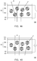
- FIG. 4A and FIG. 4B are schematic cross-sectional diagrams respectively illustrating a first implementation type of the electrically controlled light scattering switching device depicted in FIG. 1 in a scattering state and a transparent state.
- Orthogonal projections of the optical axes T1251 of the liquid crystal molecules 1251 on the first polarizer 126 are perpendicular to an anti-peep direction (e.g., the second direction D2 and its opposite direction), and the transmission axis T126 of the first polarizer 126 may be perpendicular or parallel to the anti-peep direction.
- the transmission axis T126 of the first polarizer 126 is parallel to the first direction D1
- the anti-peep direction is the second direction D2 and its opposite direction. Namely, the transmission axis T126 of the first polarizer 126 is perpendicular to the anti-peep direction, but the invention is not limited thereto.
- the backlight module 140 is located under the electrically controlled light scattering switching device 130, and the electrically controlled light scattering switching device 130 is located between the display panel 110 and the backlight module 140.
- FIG. 7 illustrates an implementation type of the backlight module 140 depicted in FIG. 1 , but the invention is not limited thereto.
- the absorptive polarizer in the filter sheet 144 may be located between the reflective polarizer and the reflection sheet 143. Additionally, an angle included between a transmission axis of the absorptive polarizer and a transmission axis (or a reflection axis) of the reflective polarizer may be adjusted to adjust a ratio of the light beams which are reflected back to the light guide plate 142, scattered by the micro-structures 1421 of light guide plate 142, and pass through the lower polarizer 112 of the display panel 110, thereby obtaining the desired brightness and anti-peep effect.
- a condition that "the angle of the reflection axis of the reflective polarizer is 0 degree, and the angle of the transmission axis of the absorptive polarizer ranges from 0 degree to 90 degrees or from 0 degree to 45 degrees" may be selected when the angle of the transmission axis of the lower polarizer of the display panel is 0 degree.
- a viewing angle switchable display apparatus 100D illustrated in FIG. 13 is similar to the viewing angle switchable display apparatus 100C illustrated in FIG. 12 , and the main difference therebetween will be described as follows.
- the polarized viewing angle control element 170 is located between the display panel 110 and the electrically controlled light scattering switching device 130, and the second polarizer 174 is located between the phase retardation film 172 and the electrically controlled light scattering switching device 130.
Landscapes
- Physics & Mathematics (AREA)
- Nonlinear Science (AREA)
- General Physics & Mathematics (AREA)
- Optics & Photonics (AREA)
- Chemical & Material Sciences (AREA)
- Crystallography & Structural Chemistry (AREA)
- Mathematical Physics (AREA)
- Liquid Crystal (AREA)
- Dispersion Chemistry (AREA)
- Optical Modulation, Optical Deflection, Nonlinear Optics, Optical Demodulation, Optical Logic Elements (AREA)
- Planar Illumination Modules (AREA)
Abstract
Description
- This application claims the priority benefit of China application serial no.
201710060681.4, filed on January 25, 2017 - The invention relates to a display apparatus and more particularly, to a viewing angle switchable display apparatus.
- Generally, a display apparatus offers a wide viewing angle display effect in order to allow multiple viewers to view displayed images together. However, in some situations or occasions (for example, when a private web page or confidential information is browsed in public, or a password is input), the wide viewing angle display effect may cause confidential information to be peeped by others which leads to leak of the confidential information. In order to satisfy anti-peep demands, a general method is to place a light control film (LCF) in front of the display apparatus to filter wide-angle light, while in a scenario with no anti-peep demands, the LCF is manually removed. It causes inconvenience in use that users have to manually place/remove the LCF. Therefore, a viewing angle control apparatus capable of adjusting the viewing angles of the display apparatus is demanded to select or adjust the display screen in a wide or a narrow viewing angle mode for the display apparatus according to operational requirements.
- The information disclosed in this Background section is only for enhancement of understanding of the background of the described technology and therefore it may contain information that does not form the prior art that is already known to a person of ordinary skill in the art. Further, the information disclosed in the Background section does not mean that one or more problems to be resolved by one or more embodiments of the invention were acknowledged by a person of ordinary skill in the art.
- The invention provides a viewing angle switchable display apparatus that controls the viewing angle in an electronically controlled manner.
- Other objectives and advantages of the invention can be further illustrated by the technical features broadly embodied and described as follows.
- In order to achieve one or a part of or all of the above advantages or other advantages, an embodiment of the invention provides a viewing angle switchable display apparatus which includes a display panel, an electrically controlled viewing angle switching device, an electrically controlled light scattering switching device and a backlight module. The electrically controlled viewing angle switching device is opposite to the display panel and includes two first transparent substrates, two first transparent conductive layers located between the two first transparent substrates, a liquid crystal layer located between the two first transparent conductive layers and a first polarizer located on a side of the electrically controlled viewing angle switching device which is far away from the display panel. The liquid crystal layer includes a plurality of liquid crystal molecules, and optical axes of the liquid crystal molecules are parallel or perpendicular to a transmission axis of the first polarizer. The electrically controlled light scattering switching device is located under the display panel and includes two second transparent substrates, two second transparent conductive layers located between the two second transparent substrates and an electronically controlled polymer material layer located between the two second transparent conductive layers. The electrically controlled light scattering switching device is located between the display panel and the backlight module.
- In view of the above, the embodiments of the invention achieve at least one of advantages or effects as listed below. In the viewing angle switchable display apparatus of the invention, the electrically controlled viewing angle switching device can be switched between an anti-peep mode and a share mode, and the electrically controlled light scattering switching device can be switched between a transparent state and a scattering state. When the electrically controlled viewing angle switching device is switched to the anti-peep mode, the electrically controlled light scattering switching device is correspondingly switched to the transparent state, such that light beams, when passing through the electrically controlled light scattering switching device, can be prevented from being scattered, and wide-angle light beams in an anti-peep direction can be absorbed when the light beams pass through the electrically controlled viewing angle switching device. Thereby, a viewer viewing the viewing angle switchable display apparatus in a wide viewing angle can be prevented from seeing a displayed image, so as to achieve an anti-peep effect. When the electrically controlled viewing angle switching device is switched to the share mode, the electrically controlled light scattering switching device is correspondingly switched to the scattering state, such that the light beams, when passing through the electrically controlled light scattering switching device, are scattered, which contributes to enlarging the viewing angle, and intensity ratios of the wide-angle light beams in the anti-peep direction are substantially uninfluenced when the light beams pass through the electrically controlled viewing angle switching device. Thus, the viewer viewing the viewing angle switchable display apparatus in the wide angle can see the displayed image, so as to achieve an image (information) sharing effect.
- Other objectives, features and advantages of the invention will be further understood from the further technological features disclosed by the embodiments of the invention wherein there are shown and described preferred embodiments of this invention, simply by way of illustration of modes best suited to carry out the invention.
- The accompanying drawings are included to provide a further understanding of the invention, and are incorporated in and constitute a part of this specification. The drawings illustrate embodiments of the invention and, together with the description, serve to explain the principles of the invention.
-
FIG. 1 is a schematic cross-sectional diagram illustrating a viewing angle switchable display apparatus according to a first embodiment of the invention. -
FIG. 2A and FIG. 2B are schematic cross-sectional diagrams respectively illustrating the electrically controlled viewing angle switching device depicted inFIG. 1 in a share mode and an anti-peep mode. -
FIG. 3 is a chart illustrating the relation between incident angle and light transmittance. -
FIG. 4A and FIG. 4B are schematic cross-sectional diagrams respectively illustrating a first implementation type of the electrically controlled light scattering switching device depicted inFIG. 1 in a scattering state and a transparent state. -
FIG. 5A and FIG. 5B are schematic cross-sectional diagrams respectively illustrating a second implementation type of the electrically controlled light scattering switching device depicted inFIG. 1 in the scattering state and the transparent state. -
FIG. 6A and FIG. 6B are schematic cross-sectional diagrams respectively illustrating a third implementation type of the electrically controlled light scattering switching device depicted inFIG. 1 in the scattering state and the transparent state. -
FIG. 7 is a schematic cross-sectional diagram illustrating the backlight module depicted inFIG. 1 . -
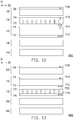
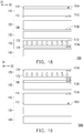
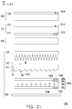
FIG. 8 to FIG. 21 are schematic cross-sectional diagrams respectively illustrating viewing angle switchable display apparatuses according to other embodiments of the invention. - In the following detailed description of the preferred embodiments, reference is made to the accompanying drawings which form a part hereof, and in which are shown by way of illustration specific embodiments in which the invention may be practiced. In this regard, directional terminology, such as "top," "bottom," "front," "back," etc., is used with reference to the orientation of the Figure(s) being described. The components of the invention can be positioned in a number of different orientations. As such, the directional terminology is used for purposes of illustration and is in no way limiting. On the other hand, the drawings are only schematic and the sizes of components may be exaggerated for clarity. It is to be understood that other embodiments may be utilized and structural changes may be made without departing from the scope of the invention. Also, it is to be understood that the phraseology and terminology used herein are for the purpose of description and should not be regarded as limiting. The use of "including," "comprising," or "having" and variations thereof herein is meant to encompass the items listed thereafter and equivalents thereof as well as additional items. Unless limited otherwise, the terms "connected," "coupled," and "mounted" and variations thereof herein are used broadly and encompass direct and indirect connections, couplings, and mountings. Similarly, the terms "facing," "faces" and variations thereof herein are used broadly and encompass direct and indirect facing, and "adjacent to" and variations thereof herein are used broadly and encompass directly and indirectly "adjacent to". Therefore, the description of "A" component facing "B" component herein may contain the situations that "A" component directly faces "B" component or one or more additional components are between "A" component and "B" component. Also, the description of "A" component "adjacent to" "B" component herein may contain the situations that "A" component is directly "adjacent to" "B" component or one or more additional components are between "A" component and "B" component. Accordingly, the drawings and descriptions will be regarded as illustrative in nature and not as restrictive.
-
FIG. 1 is a schematic cross-sectional diagram illustrating a viewing angle switchable display apparatus according to a first embodiment of the invention.FIG. 2A and FIG. 2B are schematic cross-sectional diagrams respectively illustrating the electrically controlled viewing angle switching device depicted inFIG. 1 in a share mode and an anti-peep mode.FIG. 3 is a chart illustrating the relation between incident angle and light transmittance.FIG. 4A and FIG. 4B are schematic cross-sectional diagrams respectively illustrating a first implementation type of the electrically controlled light scattering switching device depicted inFIG. 1 in a scattering state and a transparent state.FIG. 5A and FIG. 5B are schematic cross-sectional diagrams respectively illustrating a second implementation type of the electrically controlled light scattering switching device depicted inFIG. 1 in the scattering state and the transparent state.FIG. 6A and FIG. 6B are schematic cross-sectional diagrams respectively illustrating a third implementation type of the electrically controlled light scattering switching device depicted inFIG. 1 in the scattering state and the transparent state.FIG. 7 is a schematic cross-sectional diagram illustrating the backlight module depicted inFIG. 1 . - Referring to
FIG. 1 , a viewing angleswitchable display apparatus 100 includes adisplay panel 110, an electrically controlled viewingangle switching device 120, an electrically controlled lightscattering switching device 130 and abacklight module 140. Thedisplay panel 110 may be any apparatus adapted to provide images (information). For instance, thedisplay panel 110 may be a liquid crystal display panel, but the invention is not limited thereto. In addition, thedisplay panel 110 may include alower polarizer 112 and anupper polarizer 114. A transmission axis T112 of thelower polarizer 112 and a transmission axis T114 of theupper polarizer 114 may be perpendicular to each other, but the invention is not limited thereto. In another embodiment, the transmission axis T112 of thelower polarizer 112 and the transmission axis T114 of theupper polarizer 114 may also be parallel to each other. - The electrically controlled viewing
angle switching device 120 is opposite to thedisplay panel 110. For instance, thedisplay panel 110 may be located between the electrically controlled viewingangle switching device 120 and the electrically controlled lightscattering switching device 130, but the invention is not limited thereto. - Referring to
FIG. 2A , the electrically controlled viewingangle switching device 120 includes firsttransparent substrates conductive layers liquid crystal layer 125 and afirst polarizer 126. - The first
transparent substrates angle switching device 120 is more adjacent to a viewer than thedisplay panel 110, the electrically controlled lightscattering switching device 130 and thebacklight module 140, and in the electrically controlled viewingangle switching device 120, the firsttransparent substrate 122 is more adjacent to the viewer than the first transparent substrate 121 (i.e., the firsttransparent substrate 122 is further away from thedisplay panel 110 than the first transparent substrate 121). Thus, a reinforced glass substrate may be employed as the firsttransparent substrate 122, so as to increase mechanical strength of the electrically controlled viewingangle switching device 120 and contribute to omitting a protection cover of the viewing angleswitchable display apparatus 100. - The first transparent
conductive layers liquid crystal layer 125 are located between the firsttransparent substrates conductive layer 123 is located between theliquid crystal layer 125 and the firsttransparent substrate 121, and the first transparentconductive layer 124 is located between theliquid crystal layer 125 and the firsttransparent substrate 122. A material of the first transparentconductive layers - The
liquid crystal layer 125 is located between the first transparentconductive layers liquid crystal molecules 1251. Theliquid crystal molecules 1251 are adapted to deflect according to an electric field between the first transparentconductive layers liquid crystal layer 125 in different incident angles (e.g., a light beam B1 which is orthogonally incident to the electrically controlled viewingangle switching device 120, light beams B2 and B3 which are incident to the electrically controlled viewingangle switching device 120 in small angles, and light beams B4 and B5 which are incident to the electrically controlled viewingangle switching device 120 in wide angles) generate phase retardation in different degrees, thereby polarization directions of the light beams passing through theliquid crystal layer 125 with different incident angles have different degrees of change amounts. - The
first polarizer 126 is located on a side of the electrically controlled viewingangle switching device 120 which is far away from thedisplay panel 110. In the embodiment, thefirst polarizer 126 is disposed, for example, on the firsttransparent substrate 122 which is relatively far away from thedisplay panel 110. - Each of the
liquid crystal molecules 1251 has an optical axis T1251, and thefirst polarizer 126 has a transmission axis T126. In the embodiment, the transmission axis T126 of thefirst polarizer 126 is parallel to the first direction D1, and the optical axes T1251 of theliquid crystal molecules 1251 are also parallel to the first direction D1. Namely, the optical axes T1251 of theliquid crystal molecules 1251 are parallel to the transmission axis T126 of thefirst polarizer 126, but the invention is not limited thereto. In another embodiment, the optical axes T1251 of theliquid crystal molecules 1251 may also be perpendicular to the transmission axis T126 of thefirst polarizer 126. - Referring to
FIG. 1 to FIG. 2B , with the transmission axis T126 of thefirst polarizer 126 and the transmission axis T114 of theupper polarizer 114 in thedisplay panel 110 being parallel to each other, polarization states of the light beams incident to the electrically controlled viewingangle switching device 120 may be parallel to the transmission axis T126 of thefirst polarizer 126. - Referring to
FIG. 2A , when the electrically controlled viewingangle switching device 120 is turned off (i.e., no potential difference exists between the first transparentconductive layers 123 and 124), theliquid crystal molecules 1251 cause no phase retardation to the light beams with various incident angles. Thus, the polarization states of the light beams B1, B2, B3, B4 and B5 passing through theliquid crystal layer 125 are all unchanged, and thus, the light beams B1, B2, B3, B4 and B5 are capable of passing through the first polarizer 126 (referring to a curve C1 inFIG. 3 ). That is, when the electrically controlled viewingangle switching device 120 is turned off, the viewing angle is not influenced, which is referred to as a share mode. - On other hand, referring to
FIG. 2B , when the electrically controlled viewingangle switching device 120 is turned on (i.e., a potential difference exists between the first transparentconductive layers 123 and 124), theliquid crystal molecules 1251 generate the phase retardation in different degrees to the light beams with different incident angles. Thus, the polarization states of at least a part of the light beams (e.g., the light beams B2, B3, B4 and B5) passing through theliquid crystal layer 125 are changed, and light transmittance of the electrically controlled viewingangle switching device 120 in a second direction D2 (which is a direction perpendicular to the transmission axis T126 of the first polarizer 126) decreases as the incident angle increases (referring to a curve C2 inFIG. 3 ). That is, when the electrically controlled viewingangle switching device 120 is turned on, the light beams (e.g., the light beams B4 and B5) with the wide incident angles in the second direction D2 are incapable of passing through thefirst polarizer 126, which is referred to as an anti-peep mode. - Referring to
FIG. 2B and a curve C3 illustrated inFIG. 3 , when the amount of the phase retardation of theliquid crystal layer 125 is sufficiently large, the light transmittance of the electrically controlled viewingangle switching device 120 first increases and then decreases as the incident angle increases. In other words, by modulating a thickness of theliquid crystal layer 125 or a refractive index difference (ΔN, where ΔN=Ne-No) of theliquid crystal molecules 1251 to change the amount of the phase retardation of theliquid crystal layer 125, the light transmittance of the electrically controlled viewingangle switching device 120 in the second direction D2 may be further controlled, i.e., the size of the viewing angle in the second direction D2 may be further controlled. - Orthogonal projections of the optical axes T1251 of the
liquid crystal molecules 1251 on thefirst polarizer 126 are perpendicular to an anti-peep direction (e.g., the second direction D2 and its opposite direction), and the transmission axis T126 of thefirst polarizer 126 may be perpendicular or parallel to the anti-peep direction. In the embodiment, the transmission axis T126 of thefirst polarizer 126 is parallel to the first direction D1, and the anti-peep direction is the second direction D2 and its opposite direction. Namely, the transmission axis T126 of thefirst polarizer 126 is perpendicular to the anti-peep direction, but the invention is not limited thereto. In another embodiment, the transmission axis T126 of thefirst polarizer 126 may be parallel to the second direction D2, and in this circumstance, the anti-peep direction is still the second direction D2 and its opposite direction. Namely, the transmission axis T126 of thefirst polarizer 126 is parallel to the anti-peep direction. In this architecture, the transmission axis T114 of theupper polarizer 114 of thedisplay panel 110 depicted inFIG. 1 has to be changed to be parallel to the second direction D2, such that the polarization states of the light beams incident to the electrically controlled viewingangle switching device 120 are parallel to the transmission axis T126 of thefirst polarizer 126. In the architecture that the transmission axis T112 of thelower polarizer 112 and the transmission axis T114 of theupper polarizer 114 are perpendicular to each other, the transmission axis T112 of thelower polarizer 112 in thedisplay panel 110 also has to be changed to be parallel to the first direction D1. - Based on different demands, the electrically controlled viewing
angle switching device 120 may further include other film layers. For instance, the electrically controlled viewingangle switching device 120 may further includealignment layers alignment layer 127 is located between theliquid crystal layer 125 and the first transparentconductive layer 123, and thealignment layer 128 is located between theliquid crystal layer 125 and the first transparentconductive layer 124. - Referring to
FIG. 1 andFIG. 4A , the electrically controlled lightscattering switching device 130 is located under thedisplay panel 110 and between thedisplay panel 110 and thebacklight module 140. The electrically controlled lightscattering switching device 130 includes secondtransparent substrates conductive layers polymer material layer 135. - The second
transparent substrates conductive layers polymer material layer 135 are located between the secondtransparent substrates conductive layer 133 is located between the electronically controlledpolymer material layer 135 and the secondtransparent substrate 131, and the second transparentconductive layer 134 is located between the electronically controlledpolymer material layer 135 and the secondtransparent substrate 132. A material of the second transparentconductive layers polymer material layer 135 is located between the second transparentconductive layers polymer material layer 135 may include polymer dispersed liquid crystal (PDLC), polymer network liquid crystal (PNLC) or a composition containing dual frequency liquid crystal (DFLC) and reactive mesogen (RM).FIG. 4A and FIG. 4B ,FIG. 5A and FIG. 5B , andFIG. 6A and FIG. 6B respectively illustrate three implementation types of the electronically controlledpolymer material layer 135, but the invention is not limited thereto. - As illustrated in
FIG. 4A and FIG. 4B , the electronically controlledpolymer material layer 135 may include, for example, a plurality of micron-sizedliquid crystal droplets 1351 and apolymer material 1352. The micron-sizedliquid crystal droplets 1351 are distributed in thepolymer material 1352. When the electronically controlledpolymer material layer 135 is not driven by a voltage, as illustrated inFIG. 4A , the micron-sizedliquid crystal droplets 1351 present a scattering state, and the light beam B, when passing through the micron-sizedliquid crystal droplets 1351, is scattered. When the electronically controlledpolymer material layer 135 is driven by the voltage, as illustrated inFIG. 4B , the micron-sizedliquid crystal droplets 1351 present a transparent state, and most of the light beam B, when passing through the micron-sizedliquid crystal droplets 1351, is not scattered. - Additionally, as illustrated in
FIG. 5A and FIG. 5B , an electronically controlledpolymer material layer 135A may include a plurality ofliquid crystal molecules 1353 and a polymer network (PN) 1354. When the electronically controlledpolymer material layer 135A is not driven by a voltage, as illustrated inFIG. 5A , theliquid crystal molecules 1353 are dispersedly distributed and present the scattering state. When the electronically controlledpolymer material layer 135A is driven by the voltage, as illustrated inFIG. 5B , optical axes T1353 of theliquid crystal molecules 1353 are parallel to an electric field, and theliquid crystal molecules 1353 present the transparent state. - Further, as illustrated in
FIG. 6A and FIG. 6B , an electronically controlledpolymer material layer 135B may include acomposition containing DFLC 1355 and RM 1356 (or an anisotropic polymer network). Additionally, the electrically controlled lightscattering switching device 130 may further include vertical alignment layers 136 and 137. Thevertical alignment layer 136 is located between the electronically controlledpolymer material layer 135B and the second transparentconductive layer 133, and thevertical alignment layer 137 is located between the electronically controlledpolymer material layer 135B and the second transparentconductive layer 134. - When the electronically controlled
polymer material layer 135B is driven by a high-frequency voltage, as illustrated inFIG. 6A , molecule dipolar moments and optical axes theDFLC 1355 are perpendicular, and theDFLC 1355 located adjacent to the vertical alignment layers 136 and 137 and theRM 1356 is not turned by the electric field in the presence of an anchoring force, while theDFLC 1355 that is not located adjacent to the vertical alignment layers 136 and 137 and thereactive RM 1356 is turned by the electric field and presents the scattering state as a part of theDFLC 1355 is perpendicular to a direction of the electric field, and another part of theDFLC 1355 is parallel to the direction of the electric field. When the electronically controlledpolymer material layer 135B is not driven by the voltage or driven by a low-frequency voltage, as illustrated inFIG. 6B , theDFLC 1355 and theRM 1356 present the transparent state as the molecule dipolar moments and the optical axes of theDFLC 1355 are parallel, and the optical axes of theDFLC 1355 and theRM 1356 are substantially parallel to the direction of the electric field. Additionally, by comparing the transparent states illustrated inFIG. 4B andFIG. 5B , since extraordinary refractive indices and ordinary refractive indices of theDFLC 1355 and theRM 1356 are similar to each other, and the scattering of inclined incident light may be suppressed in the transparent state, an included angle between the inclined incident light emitting from the electrically controlled lightscattering switching device 130 and a normal vector of the secondtransparent substrate 132 is small (with reference to the rightmost light beam B illustrated inFIG. 4B ,FIG. 5B andFIG. 6B ), thereby enhancing an anti-peep effect. - Referring to
FIG. 1 andFIG. 7 , thebacklight module 140 is located under the electrically controlled lightscattering switching device 130, and the electrically controlled lightscattering switching device 130 is located between thedisplay panel 110 and thebacklight module 140.FIG. 7 illustrates an implementation type of thebacklight module 140 depicted inFIG. 1 , but the invention is not limited thereto. - Referring to
FIG. 7 , thebacklight module 140 may include alight source 141, alight guide plate 142, areflection sheet 143, afilter sheet 144 and areverse prism film 145. Thelight source 141 is located at a side of thelight guide plate 142. Thelight guide plate 142 is located between thereverse prism film 145 and thereflection sheet 143. Thefilter sheet 144 is located between thelight guide plate 142 and thereflection sheet 143. - In addition, the
light guide plate 142 has a light-incident surface SI, a bottom surface SB and a light-emitting surface SE. The light-incident surface SI is connected with the bottom surface SB and the light-emitting surface SE, and a plurality of micro-structures 1421 may be formed on the bottom surface SB. Thelight source 141 is located next to the light-incident surface SI of thelight guide plate 142 and adapted to emit illumination light beams toward the light-incident surface SI. Thereflection sheet 143 and thefilter sheet 144 are disposed under the bottom surface SB, and thereverse prism film 145 is disposed above the light-emitting surface SE. In the embodiment, extension directions of the micro-structures 1421 and cylindrical prisms (not noted) of thereverse prism film 145 are respectively parallel to the anti-peep direction (i.e., the second direction D2 and its opposite direction), but the invention is not limited thereto. In another embodiment, the extension directions of the micro-structures 1421 and the cylindrical prisms of thereverse prism film 145 may also be respectively perpendicular to the anti-peep direction. - The disposition of the
filter sheet 144 is adapted to reduce the light beams reflected back to thelight guide plate 142 by thereflection sheet 143, so as to prevent the light beams from being scattered by themicro-structures 1421 of thelight guide plate 142, sand thus reducing the probability of the generation of inclined scattering light. In this way, a preferable anti-peep effect may be achieved. For instance, thefilter sheet 144 may be a translucent film containing a light absorbing material (e.g., a dye), an absorptive polarizer, or a composite polarizer composed of an absorptive polarizer and a reflective polarizer. In an embodiment, the disposition of thefilter sheet 144 may be omitted. Additionally, a reflection sheet with a lower reflectivity (which is lower than 50%, for example) may be used in replacement with an ordinary reflection sheet with a higher reflectivity (which is higher than 90%, for example), so as to further enhance the anti-peep effect. - When the
filter sheet 144 is a translucent film containing a light absorbing material, the lower the absorbance of thefilter sheet 144, the higher the light transmittance. In other words, as the absorbance of thefilter sheet 144 decreases, the light beams reflected back to thelight guide plate 142 by thereflection sheet 143 increase. Therefore, the higher the brightness of thedisplay panel 110, the poorer the anti-peep effect. When the light transmittance of thefilter sheet 144 is more than 60%, thedisplay panel 110 has a higher brightness and a poorer anti-peep effect. When the light transmittance of thefilter sheet 144 is less than 60%, thedisplay panel 110 has a lower brightness, but a better anti-peep effect. - Referring to
FIG. 1 andFIG. 7 , when thefilter sheet 144 is an absorptive polarizer, a higher brightness may be obtained if a transmission axis (not shown) of the absorptive polarizer is parallel to the transmission axis T112 of thelower polarizer 112 of thedisplay panel 110, but a pooper anti-peep effect may be obtained as more light beams are reflected back to thelight guide plate 142 by thereflection sheet 143. If the transmission axis of the absorptive polarizer is perpendicular to the transmission axis T112 of thelower polarizer 112 of thedisplay panel 110, the brightness of thedisplay panel 110 may be lower, but a higher portion of the light beams which are reflected back to thelight guide plate 142 by thereflection sheet 143 are absorbed by thelower polarizer 112 of thedisplay panel 110, and thus, the anti-peep effect may be preferable. Accordingly, the included angle between the transmission axis of the absorptive polarizer and the transmission axis T112 of thelower polarizer 112 of thedisplay panel 110 may be adjusted according to the desired brightness and anti-peep effect. - When the
filter sheet 144 is a composite polarizer composed of an absorptive polarizer and a reflective polarizer, the absorptive polarizer in thefilter sheet 144 may be located between the reflective polarizer and thereflection sheet 143. Additionally, an angle included between a transmission axis of the absorptive polarizer and a transmission axis (or a reflection axis) of the reflective polarizer may be adjusted to adjust a ratio of the light beams which are reflected back to thelight guide plate 142, scattered by themicro-structures 1421 oflight guide plate 142, and pass through thelower polarizer 112 of thedisplay panel 110, thereby obtaining the desired brightness and anti-peep effect. - Table 1 shows influence on the brightness and the anti-peep effect by the relative relation among an angle of the transmission axis of the lower polarizer of the display panel, an angle of the reflection axis of the reflective polarizer of the filter sheet (which has an included angle of 90 degrees with the transmission axis of the reflective polarizer), and an angle of the transmission axis of the absorptive polarizer of the filter sheet. In Table 1, numbers 1 to 4 are used to represent good and bad of the brightness of the display panel and the anti-peep effect. Particularly, in term of the brightness of the display panel, the greater number represents the higher brightness. In term of the anti-peep effect, the greater number represents the better anti-peep effect. It should be additionally mentioned that in Table 1, the angle of the transmission axis of the lower polarizer of the display panel is indicated as 0 degree only for descriptive convenience, and actually, the angle of the transmission axis of the lower polarizer of the display panel may by any other angle, and evaluations of the brightness of the display panel and the anti-peep effect will remain unchanged as long as the angles of and the relative included angle between the reflection axis of the reflective polarizer and the transmission axis of the absorptive polarizer remain unchanged.
Table 1 Condition 1 Condition 2 Condition 3 Condition 4 Angle (°) of transmission axis of lower polarizer of display panel 0 0 0 0 Angle (°) of reflection axis of reflective polarizer of filter sheet 0 0 90 90 Angle (°) of transmission axis of absorptive polarizer of filter sheet 0 90 0 90 Brightness of display panel 4 3 2 1 Anti-peep effect 2 1 3 4 - Additionally, in the filter sheet, when the angle of the reflection axis of the reflective polarizer and the angle of the transmission axis of the absorptive polarizer are not 0 degree or 90 degrees, the evaluations of the brightness of the display panel and the anti-peep effect fall within the ranges corresponding to the angles. For example, when the angle of the transmission axis of the lower polarizer of the display panel is 0 degree, the angle of the reflection axis of the reflective polarizer is 0 degree, and the angle of the transmission axis of the absorptive polarizer is 20 degrees, the evaluation of the brightness of the display panel ranges between 4 and 3, and the evaluation of the anti-peep effect ranges between 2 and 1. Thus, if a higher brightness of the display panel but a less good anti-peep effect are desired, a condition that "the angle of the reflection axis of the reflective polarizer is 0 degree, and the angle of the transmission axis of the absorptive polarizer ranges from 0 degree to 90 degrees or from 0 degree to 45 degrees" may be selected when the angle of the transmission axis of the lower polarizer of the display panel is 0 degree. If a lower brightness of the display panel but a better anti-peep effect are desired, a condition that "the angle of the reflection axis of the reflective polarizer is 90 degrees, and the angle of the transmission axis of the absorptive polarizer ranges from 0 degree to 90 degrees or from 45 degrees to 90 degrees" may be selected when the angle of the transmission axis of the lower polarizer of the display panel is 0 degree.
-
FIG. 8 to FIG. 21 are schematic cross-sectional diagrams respectively illustrating viewing angle switchable display apparatuses according to other embodiments of the invention. Therein, the display panel, the electrically controlled light scattering switching device and the backlight module of the viewing angle switchable display apparatus are respectively omitted inFIG. 8 and FIG. 9 . The same or similar reference numerals represent the same or similar elements in the following embodiments, and the related contents may refer to the corresponding descriptions with respect to the embodiments illustrated inFIG. 1 to FIG. 7 and will not be repeated hereinafter. - Referring to
FIG. 8 , the viewing angle switchable display apparatus may further include atouch sensing element 150 to provide a touch sensing function. Thetouch sensing element 150 may be located between thefirst polarizer 126 and the firsttransparent substrate 122 and have single-layer or multi-layer touch sensing electrodes (not shown). The touch sensing electrodes may be disposed on the firsttransparent substrate 122 or thefirst polarizer 126. Alternatively, the multi-layer touch sensing electrodes may be respectively disposed on the firsttransparent substrate 122 and thefirst polarizer 126, and then attached thereto through an insulated transparent adhesive layer. Moreover, the touch sensing electrodes may be disposed on at least one thin film or at least one substrate (which is not shown) in advance and then attached to the firsttransparent substrate 122 and thefirst polarizer 126 through a transparent adhesive layer. - In addition, the viewing angle switchable display apparatus may further include a
decoration layer 160. Thedecoration layer 160 is located on the electrically controlled viewingangle switching device 120, and thefirst polarizer 126 is located between thedecoration layer 160 and thetouch sensing element 150. Thedecoration layer 160 is disposed, for example, in the periphery of thefirst polarizer 126 to shield the elements (for example, peripheral traces of the touch sensing element 150) that are not desired to be seen. Additionally, thedecoration layer 160 exposes a display region of thedisplay panel 110, so as to prevent display light beams from being shielded. Thedecoration layer 160 may be made of ink or other light absorbing material. - In yet another embodiment, as illustrated in
FIG. 9 , thetouch sensing element 150 may also be located on thefirst polarizer 126. Particularly, thetouch sensing element 150 and thedecoration layer 160 may be sequentially stacked on the electrically controlled viewingangle switching device 120, and thereby, thetouch sensing element 150 is located between thedecoration layer 160 and thefirst polarizer 126. - Referring to
FIG. 1 andFIG. 10 , a viewing angleswitchable display apparatus 100A illustrated inFIG. 10 is similar to the viewing angleswitchable display apparatus 100 inFIG. 1 , and the main difference therebetween will be described as follows. In the viewing angleswitchable display apparatus 100 illustrated inFIG. 1 , thedisplay panel 110 is located between the electrically controlled viewingangle switching device 120 and the electrically controlled lightscattering switching device 130, and thefirst polarizer 126 is disposed on the first transparent substrate 122 (referring toFIG. 2A ). In the viewing angleswitchable display apparatus 100A illustrated inFIG. 10 , the electrically controlled viewingangle switching device 120 is located between thedisplay panel 110 and the electrically controlled lightscattering switching device 130, and thefirst polarizer 126 is disposed on a side of the first transparent substrate 121 (referring toFIG. 2A ) which is far away from thedisplay panel 110, and thereby, the firsttransparent substrate 121 is located between thefirst polarizer 126 and the first transparentconductive layer 123. Additionally, the transmission axis T126 of thefirst polarizer 126 is parallel to the transmission axis of one of the polarizers in thedisplay panel 110 which is adjacent to thefirst polarizer 126, for example, the transmission axis T112 of thelower polarizer 112. - Referring to
FIG. 1 andFIG. 11 , a viewing angleswitchable display apparatus 100B illustrated inFIG. 11 is similar to the viewing angleswitchable display apparatus 100 illustrated inFIG. 1 , and the main difference therebetween will be described as follows. The viewing angleswitchable display apparatus 100B illustrated inFIG. 11 further includes a polarized viewingangle control element 170. The polarized viewingangle control element 170 is located above thebacklight module 140 and includes aphase retardation film 172 and asecond polarizer 174. Thesecond polarizer 174 is disposed on a side of thephase retardation film 172 which is far away from thedisplay panel 110. In the embodiment, the polarized viewingangle control element 170 is located on the electrically controlled viewingangle switching device 120, and thereby, the electrically controlled viewingangle switching device 120 is located between the polarized viewingangle control element 170 and thedisplay panel 110, and thephase retardation film 172 is located between thesecond polarizer 174 and the electrically controlled viewingangle switching device 120. - The
phase retardation film 172 is, for example, a C-plate, where an optical axis T172 of thephase retardation film 172 is perpendicular to thesecond polarizer 174. Thesecond polarizer 174 is, for example, an absorptive polarizer, and a transmission axis T174 of thesecond polarizer 174 is parallel to a transmission axis T126 of thefirst polarizer 126. In this architecture, the polarized viewingangle control element 170 may further filter the light beams which have included angles ranging 45±15 degrees with the anti-peep direction (e.g., the second direction D2 and its opposite direction) at an azimuth, thereby enlarging an anti-peep angle range at the azimuth. - In another embodiment, the
phase retardation film 172 may also be an O-plate. In this way, the polarized viewingangle control element 170 may further enlarge the angle range for filtering the light beams in the anti-peep direction, such that the anti-peep angle range in the anti-peep direction may be enlarged. In yet another embodiment, thephase retardation film 172 may also be a composite plate composed of an O-plate and a C-plate to enlarge the anti-peep angle range at the azimuth and the anti-peep angle range in the anti-peep direction. - Referring to
FIG. 11 andFIG. 12 , a viewing angleswitchable display apparatus 100C illustrated inFIG. 12 is similar to the viewing angleswitchable display apparatus 100B illustrated inFIG. 11 , and the main difference therebetween will be described as follows. In the viewing angleswitchable display apparatus 100C illustrated inFIG. 12 , the polarized viewingangle control element 170 is located between the electrically controlled viewingangle switching device 120 and thedisplay panel 110, and thephase retardation film 172 is located between thesecond polarizer 174 and thedisplay panel 110. - Referring to
FIG. 12 and FIG. 13 , a viewing angleswitchable display apparatus 100D illustrated inFIG. 13 is similar to the viewing angleswitchable display apparatus 100C illustrated inFIG. 12 , and the main difference therebetween will be described as follows. In the viewing angleswitchable display apparatus 100D illustrated inFIG. 13 , the polarized viewingangle control element 170 is located between thedisplay panel 110 and the electrically controlled lightscattering switching device 130, and thesecond polarizer 174 is located between thephase retardation film 172 and the electrically controlled lightscattering switching device 130. Additionally, the transmission axis T174 of thesecond polarizer 174 is parallel to the transmission axis of one of the polarizers in thedisplay panel 110 which is adjacent to thesecond polarizer 174, for example, the transmission axis T112 of thelower polarizer 112. - Referring to
FIG. 13 andFIG. 14 , a viewing angleswitchable display apparatus 100E illustrated inFIG. 14 is similar to the viewing angleswitchable display apparatus 100D illustrated inFIG. 13 , and the main difference therebetween will be described as follows. In the viewing angleswitchable display apparatus 100E illustrated inFIG. 14 , the polarized viewingangle control element 170 is located between the electrically controlled lightscattering switching device 130 and thebacklight module 140, and thesecond polarizer 174 is located between thephase retardation film 172 and thebacklight module 140. - Referring to
FIG. 10 andFIG. 15 , a viewing angleswitchable display apparatus 100F illustrated inFIG. 15 is similar to the viewing angleswitchable display apparatus 100A illustrated inFIG. 10 , and the main difference therebetween will be described as follows. The viewing angleswitchable display apparatus 100F illustrated inFIG. 15 further includes a polarized viewingangle control element 170, and therein, the description related to each film layer in the polarized viewingangle control element 170 may refer to the related descriptions corresponding to the polarized viewingangle control element 170 illustrated inFIG. 11 and will not be repeated hereinafter. - Referring to
FIG. 15 andFIG. 16 , a viewing angleswitchable display apparatus 100G illustrated inFIG. 16 is similar to the viewing angleswitchable display apparatus 100F illustrated inFIG. 15 , and the main difference therebetween will be described as follows. In the viewing angleswitchable display apparatus 100G illustrated inFIG. 16 , the polarized viewingangle control element 170 is located between thedisplay panel 110 and the electrically controlled viewingangle switching device 120, and thesecond polarizer 174 is located between thephase retardation film 172 and the electrically controlled viewingangle switching device 120. Additionally, the transmission axis T174 of thesecond polarizer 174 is parallel to the transmission axis of one of the polarizers in thedisplay panel 110 which is adjacent to thesecond polarizer 174, for example, the transmission axis T112 of thelower polarizer 112. - Referring to
FIG. 16 and FIG. 17 , a viewing angleswitchable display apparatus 100H illustrated inFIG. 17 is similar to the viewing angleswitchable display apparatus 100G illustrated inFIG. 16 , and the main difference therebetween will be described as follows. In the viewing angleswitchable display apparatus 100H illustrated inFIG. 17 , the polarized viewingangle control element 170 is located between the electrically controlled viewingangle switching device 120 and the electrically controlled lightscattering switching device 130, and thesecond polarizer 174 is located between thephase retardation film 172 and the electrically controlled lightscattering switching device 130. - Referring to
FIG. 17 andFIG. 18 , a viewing angle switchable display apparatus 100I illustrated inFIG. 18 is similar to the viewing angleswitchable display apparatus 100H illustrated inFIG. 17 , and the main difference therebetween will be described as follows. In the viewing angle switchable display apparatus 100I illustrated inFIG. 18 , the polarized viewingangle control element 170 is located between the electrically controlled lightscattering switching device 130 and thebacklight module 140, and thesecond polarizer 174 is located between thephase retardation film 172 and thebacklight module 140. - Referring to
FIG. 11 andFIG. 19 , a viewing angleswitchable display apparatus 100J illustrated inFIG. 19 is similar to the viewing angleswitchable display apparatus 100B illustrated inFIG. 11 , and the main difference therebetween will be described as follows. In the viewing angleswitchable display apparatus 100J illustrated inFIG. 19 , the transmission axis T112 of thelower polarizer 112 of thedisplay panel 110 is parallel to the first direction D1, and the transmission axis T114 of theupper polarizer 114 of thedisplay panel 110, the transmission axis T126 of thefirst polarizer 126 and the transmission axis T174 of thesecond polarizer 174 are parallel to the second direction D2. Additionally, thephase retardation film 172 is an O-plate, where the optical axis T172 of thephase retardation film 172 is inclined relatively to the first direction D1. Namely, the optical axis T172 of thephase retardation film 172 is neither perpendicular nor parallel to the first direction D1. Additionally, an orthogonal projection of the optical axis T172 of thephase retardation film 172 on thesecond polarizer 174 is perpendicular to the second direction D2 (i.e., the anti-peep direction). - It should be supplementarily noted that although the aforementioned modifications of the embodiment are made based on the architecture illustrated in
FIG. 11 , the modifications (including replacing the C-plate with the O-plate and changing the directions of the transmission axes of the plurality of film layers) may also be applicable to the embodiments illustrated inFIG. 12 to FIG. 18 . - Referring to
FIG. 1 andFIG. 20 , a viewing angleswitchable display apparatus 100K illustrated inFIG. 20 is similar to the viewing angleswitchable display apparatus 100 illustrated inFIG. 1 , and the main difference therebetween will be described as follows. In the viewing angleswitchable display apparatus 100K, thefilter sheet 144 depicted inFIG. 7 is replaced by a polarized viewingangle control element 180. The polarized viewingangle control element 180 is located between thelight guide plate 142 and thereflection sheet 143 and includesthird polarizers phase retardation film 186 located between thethird polarizers - Each of the
third polarizers third polarizer 182 and a transmission axis T184 of thethird polarizer 184 are respectively parallel to the transmission axis T112 of thelower polarizer 112 of thedisplay panel 110. For instance, both of thethird polarizers third polarizer 182 may be an absorptive polarizer, and thethird polarizer 184 may be a reflective polarizer. - The
phase retardation film 186 may be an O-plate or a C-plate. In other words, an optical axis T186 of thephase retardation film 186 may be perpendicular to thethird polarizer 182. Alternatively, the optical axis T186 of thephase retardation film 186 may be inclined relatively to the first direction D1, and an orthogonal projection of the optical axis T186 of thephase retardation film 186 on thethird polarizer 182 is perpendicular to the second direction D2 (i.e., the anti-peep direction). - A polarized viewing
angle control element 180 is adapted to filter light beams at angles ranging from 60 degrees to 80 degrees, and may prevent leakage of large-viewing-angle light resulted from the light beams reflected back to thelight guide plate 142 by thereflection sheet 143 and scattered by themicro-structures 1421 of thelight guide plate 142, so as to enhance the anti-peep effect. - It should be supplementarily noted that although the aforementioned modification of the embodiment is made based on the architecture illustrated in
FIG. 1 , the modification (i.e., replacing thefilter sheet 144 illustrated inFIG. 7 with the polarized viewing angle control element 180) may also be applicable to other embodiments. - Referring to
FIG. 20 andFIG. 21 , a viewing angleswitchable display apparatus 100L illustrated inFIG. 21 is similar to the viewing angleswitchable display apparatus 100K illustrated inFIG. 20 , and the main difference therebetween will be described as follows. In the viewing angleswitchable display apparatus 100L illustrated inFIG. 21 , thethird polarizers angle control element 180A are respectively absorptive polarizers, and the polarized viewingangle control element 180A further includes a reflective polarizer 188. The reflective polarizer 188 is located on a side of the polarized viewingangle control element 180A which is adjacent to thelight guide plate 142. Particularly, the reflective polarizer 188 is, for example, disposed on thethird polarizer 184, and thethird polarizer 184 is located between the reflective polarizer 188 and thephase retardation film 186. A transmission axis T188 of the reflective polarizer 188 is parallel to the transmission axis T182 of thethird polarizer 182 and the transmission axis T184 of thethird polarizer 184. Thereby, the brightness of thedisplay panel 110 may be increased. - In light of the foregoing, the embodiments of the invention achieve at least one of the following advantages or effects. In the viewing angle switchable display apparatus of the invention, the electrically controlled viewing angle switching device can be switched between the anti-peep mode and the share mode, and the electrically controlled light scattering switching device can be switched between the transparent state and the scattering state. When the electrically controlled viewing angle switching device is switched to the anti-peep mode, the electrically controlled light scattering switching device is correspondingly switched to the transparent state, such that the light beams, when passing through the electrically controlled light scattering switching device, can be prevented from being scattered, and the wide-angle light beams in the anti-peep direction are absorbed when the light beams pass through the electrically controlled viewing angle switching device. Thereby, the viewer viewing the viewing angle switchable display apparatus in a wide viewing angle can be prevented from seeing a displayed image, so as to achieve the anti-peep effect. When the electrically controlled viewing angle switching device is switched to the share mode, the electrically controlled light scattering switching device is correspondingly switched to the scattering state, such that the light beams, when passing through the electrically controlled light scattering switching device, are scattered, which contributes to enlarging the viewing angle, and the intensity ratios of the wide-angle light beams in the anti-peep direction are substantially uninfluenced when the light beams pass through the electrically controlled viewing angle switching device. Thus, the viewer viewing the viewing angle switchable display apparatus in the wide angle can see the displayed image, so as to achieve an image (information) sharing effect.
- The foregoing description of the preferred embodiments of the invention has been presented for purposes of illustration and description. It is not intended to be exhaustive or to limit the invention to the precise form or to exemplary embodiments disclosed. Accordingly, the foregoing description should be regarded as illustrative rather than restrictive. Obviously, many modifications and variations will be apparent to practitioners skilled in this art. The embodiments are chosen and described in order to best explain the principles of the invention and its best mode practical application, thereby to enable persons skilled in the art to understand the invention for various embodiments and with various modifications as are suited to the particular use or implementation contemplated. It is intended that the scope of the invention be defined by the claims appended hereto and their equivalents in which all terms are meant in their broadest reasonable sense unless otherwise indicated. Therefore, the term "the invention", "the invention" or the like does not necessarily limit the claim scope to a specific embodiment, and the reference to particularly preferred exemplary embodiments of the invention does not imply a limitation on the invention, and no such limitation is to be inferred. The invention is limited only by the spirit and scope of the appended claims. The abstract of the disclosure is provided to comply with the rules requiring an abstract, which will allow a searcher to quickly ascertain the subject matter of the technical disclosure of any patent issued from this disclosure. It is submitted with the understanding that it will not be used to interpret or limit the scope or meaning of the claims. Any advantages and benefits described may not apply to all embodiments of the invention. It should be appreciated that variations may be made in the embodiments described by persons skilled in the art without departing from the scope of the invention as defined by the following claims. Moreover, no element and component in the present disclosure is intended to be dedicated to the public regardless of whether the element or component is explicitly recited in the following claims.
Claims (14)
- A viewing angle switchable display apparatus, comprising:a display panel;an electrically controlled viewing angle switching device, opposite to the display panel and comprising two first transparent substrates, two first transparent conductive layers located between the two first transparent substrates, a liquid crystal layer located between the two first transparent conductive layers and a first polarizer located on a side of the electrically controlled viewing angle switching device which is far away from the display panel, wherein the liquid crystal layer comprises a plurality of liquid crystal molecules, and optical axes of the liquid crystal molecules are parallel or perpendicular to a transmission axis of the first polarizer;an electrically controlled light scattering switching device, comprising two second transparent substrates, two second transparent conductive layers located between the two second transparent substrates and an electronically controlled polymer material layer located between the two second transparent conductive layers; anda backlight module, wherein the electrically controlled light scattering switching device is located between the display panel and the backlight module.
- The viewing angle switchable display apparatus according to claim 1, wherein the display panel is located between the electrically controlled viewing angle switching device and the electrically controlled light scattering switching device.
- The viewing angle switchable display apparatus according to claim 2, wherein one of the two first transparent substrates which is far away from the display panel is a reinforced glass substrate.
- The viewing angle switchable display apparatus according to claim 2, further comprising:a touch sensing element, located between the first polarizer and one of the two first transparent substrates which is far away from the display panel; anda decoration layer, located on the electrically controlled viewing angle switching device, wherein the first polarizer is located between the decoration layer and the touch sensing element.
- The viewing angle switchable display apparatus according to claim 2, further comprising:a touch sensing element, located on the first polarizer; anda decoration layer, located on the touch sensing element, wherein the touch sensing element is located between the decoration layer and the first polarizer.
- The viewing angle switchable display apparatus according to claim 1, wherein the electrically controlled viewing angle switching device is located between the display panel and the electrically controlled light scattering switching device.
- The viewing angle switchable display apparatus according to claim 1, wherein the electronically controlled polymer material layer comprises polymer dispersed liquid crystal, polymer network liquid crystal or a composition containing dual frequency liquid crystal and reactive mesogen.
- The viewing angle switchable display apparatus according to claim 1, wherein the backlight module comprises a light source, a light guide plate, a reflection sheet, a filter sheet and a reverse prism film, the light source is located at a side of the light guide plate, the light guide plate is located between the reverse prism film and the reflection sheet, and the filter sheet is located between the light guide plate and the reflection sheet.
- The viewing angle switchable display apparatus according to claim 8, wherein the filter sheet is a translucent film containing a light absorbing material, an absorptive polarizer or a composite polarizer composed of an absorptive polarizer and a reflective polarizer.
- The viewing angle switchable display apparatus according to claim 1, further comprising:a polarized viewing angle control element, located above the backlight module and comprising a phase retardation film and a second polarizer, wherein the second polarizer is disposed on a side of the phase retardation film which is far away from the display panel.
- The viewing angle switchable display apparatus according to claim 10, wherein the phase retardation film is an O-plate, a C-plate or a composite plate composed of an O-plate and a C-plate.
- The viewing angle switchable display apparatus according to claim 1, further comprising:a polarized viewing angle control element, located between a light guide plate and a reflection sheet, wherein the polarized viewing angle control element comprises two third polarizers and a phase retardation film located between the two third polarizers.
- The viewing angle switchable display apparatus according to claim 12, wherein each of the two third polarizers is an absorptive polarizer or a reflective polarizer, and the phase retardation film is an O-plate or a C-plate.
- The viewing angle switchable display apparatus according to claim 12, wherein each of the two third polarizers is an absorptive polarizer, the phase retardation film is an O-plate or a C-plate, and the polarized viewing angle control element further comprises a reflective polarizer located on a side of the polarized viewing angle control element which is adjacent to the light guide plate.
Applications Claiming Priority (1)
| Application Number | Priority Date | Filing Date | Title |
|---|---|---|---|
| CN201710060681.4A CN108345139B (en) | 2017-01-25 | 2017-01-25 | Viewing angle switchable display device |
Publications (2)
| Publication Number | Publication Date |
|---|---|
| EP3355105A1 true EP3355105A1 (en) | 2018-08-01 |
| EP3355105B1 EP3355105B1 (en) | 2020-08-12 |
Family
ID=60654828
Family Applications (1)
| Application Number | Title | Priority Date | Filing Date |
|---|---|---|---|
| EP17206365.3A Active EP3355105B1 (en) | 2017-01-25 | 2017-12-11 | Viewing angle switchable display apparatus |
Country Status (5)
| Country | Link |
|---|---|
| US (1) | US11402676B2 (en) |
| EP (1) | EP3355105B1 (en) |
| JP (1) | JP7114247B2 (en) |
| CN (1) | CN108345139B (en) |
| TW (1) | TWI612360B (en) |
Cited By (2)
| Publication number | Priority date | Publication date | Assignee | Title |
|---|---|---|---|---|
| TWI718641B (en) * | 2019-08-16 | 2021-02-11 | 中強光電股份有限公司 | View angle control structure and display apparatus |
| TWI718820B (en) * | 2019-12-11 | 2021-02-11 | 中強光電股份有限公司 | Backlight module and display apparatus |
Families Citing this family (85)
| Publication number | Priority date | Publication date | Assignee | Title |
|---|---|---|---|---|
| WO2017074951A1 (en) | 2015-10-26 | 2017-05-04 | Reald Inc. | Intelligent privacy system, apparatus, and method thereof |
| CN114554177A (en) | 2016-05-19 | 2022-05-27 | 瑞尔D斯帕克有限责任公司 | Wide-angle imaging directional backlight |
| CN107664871B (en) * | 2016-07-27 | 2020-03-31 | 京东方科技集团股份有限公司 | Backlight module and display device |
| CN108345139B (en) | 2017-01-25 | 2022-04-22 | 中强光电股份有限公司 | Viewing angle switchable display device |
| CN106646955A (en) * | 2017-03-07 | 2017-05-10 | 京东方科技集团股份有限公司 | Peep-proof display device and peep-proof display method |
| US10126575B1 (en) | 2017-05-08 | 2018-11-13 | Reald Spark, Llc | Optical stack for privacy display |
| JP7204073B2 (en) | 2017-05-08 | 2023-01-16 | リアルディー スパーク エルエルシー | Optical stacks for directional displays |
| US20210199879A1 (en) | 2017-05-08 | 2021-07-01 | Reald Spark, Llc | Optical stack for imaging directional backlights |
| TWI878209B (en) * | 2017-09-15 | 2025-04-01 | 美商瑞爾D斯帕克有限責任公司 | Display device and a view angle control optical element for application to a display device |
| US10948648B2 (en) | 2017-09-29 | 2021-03-16 | Reald Spark, Llc | Backlights having stacked waveguide and optical components with different coefficients of friction |
| WO2019090252A1 (en) | 2017-11-06 | 2019-05-09 | Reald Spark, Llc | Privacy display apparatus |
| CN207650518U (en) | 2017-12-26 | 2018-07-24 | 扬升照明股份有限公司 | Viewing angle switchable device and viewing angle switchable display module |
| TWI827580B (en) | 2018-01-25 | 2024-01-01 | 美商瑞爾D斯帕克有限責任公司 | Reflective optical stack for privacy display |
| US20250306423A1 (en) * | 2018-01-25 | 2025-10-02 | Reald Spark, Llc | Touch screen for privacy display |
| KR102759510B1 (en) | 2018-01-25 | 2025-02-04 | 리얼디 스파크, 엘엘씨 | Touchscreen for privacy display |
| EP3769516B1 (en) | 2018-03-22 | 2025-06-25 | RealD Spark, LLC | Optical waveguide for directional backlight |
| CN110361883B (en) | 2018-03-26 | 2023-04-28 | 中强光电股份有限公司 | Anti-peeping control device and backlight module and display using same |
| CN208126055U (en) | 2018-04-28 | 2018-11-20 | 扬升照明股份有限公司 | Display device |
| US10955715B2 (en) | 2018-06-29 | 2021-03-23 | Reald Spark, Llc | Optical stack for privacy display |
| CN112602011A (en) | 2018-07-18 | 2021-04-02 | 瑞尔D斯帕克有限责任公司 | Optical stack for switchable directional display |
| WO2020072643A1 (en) | 2018-10-03 | 2020-04-09 | Reald Spark, Llc | Privacy display control apparatus |
| CN111090191B (en) * | 2018-10-24 | 2022-10-04 | 中强光电股份有限公司 | Light source module and dual-screen display device |
| WO2020097156A1 (en) | 2018-11-07 | 2020-05-14 | Reald Spark, Llc | Directional display apparatus |
| CN111338105A (en) * | 2018-12-18 | 2020-06-26 | 群创光电股份有限公司 | Display device |
| WO2020146091A1 (en) | 2019-01-07 | 2020-07-16 | Reald Spark, Llc | Optical stack for privacy display |
| CN111458911B (en) * | 2019-01-18 | 2024-03-19 | 中强光电股份有限公司 | Display device and light source module thereof |
| EP3924776B1 (en) | 2019-02-12 | 2024-07-10 | RealD Spark, LLC | Display device with diffuser for privacy display |
| CN111796438B (en) | 2019-04-09 | 2024-07-26 | 中强光电股份有限公司 | Viewing angle switching module and display device |
| CN111965888B (en) * | 2019-05-20 | 2023-08-29 | 群创光电股份有限公司 | Display apparatus |
| GB2584416A (en) | 2019-05-23 | 2020-12-09 | Flexenable Ltd | Integrated privacy windows for liquid crystal displays |
| TWI729396B (en) * | 2019-05-28 | 2021-06-01 | 友達光電股份有限公司 | Display module |
| US11402692B2 (en) | 2019-05-29 | 2022-08-02 | Coretronic Corporation | Backlight module having an optical film and display apparatus having the same |
| CN112015000B (en) * | 2019-05-29 | 2024-01-23 | 中强光电股份有限公司 | Backlight module and display device |
| CN210123503U (en) * | 2019-06-24 | 2020-03-03 | 中强光电股份有限公司 | Screen privacy protection layer and touch display device |
| TWI912252B (en) | 2019-07-02 | 2026-01-21 | 美商瑞爾D斯帕克有限責任公司 | Directional display apparatus |
| US11366353B2 (en) * | 2019-07-23 | 2022-06-21 | Innolux Corporation | Electronic device |
| WO2021026018A1 (en) | 2019-08-02 | 2021-02-11 | Reald Spark, Llc | Optical stack for privacy display |
| CN112394558B (en) | 2019-08-14 | 2023-08-08 | 中强光电股份有限公司 | Electric control visual angle switcher and display device |
| CN110501833B (en) * | 2019-08-27 | 2022-09-02 | 厦门天马微电子有限公司 | Display device |
| KR102854553B1 (en) | 2019-09-02 | 2025-09-03 | 삼성전자주식회사 | Electronic apparatus for controlling a passenger seat display and method for controlling the passenger seat display |
| EP4438945B1 (en) | 2019-10-02 | 2025-09-03 | RealD Spark, LLC | Privacy display apparatus |
| WO2021097040A1 (en) | 2019-11-13 | 2021-05-20 | Reald Spark, Llc | Display device with uniform off-axis luminance reduction |
| WO2021118936A1 (en) | 2019-12-10 | 2021-06-17 | Reald Spark, Llc | Control of reflections of a display device |
| CN114902093B (en) | 2019-12-18 | 2025-09-26 | 瑞尔D斯帕克有限责任公司 | Ambient light control for privacy displays |
| KR102714565B1 (en) * | 2019-12-31 | 2024-10-07 | 엘지디스플레이 주식회사 | Privacy protecting film and liquid crystal display device comrpising the same |
| JP7304296B2 (en) * | 2020-01-17 | 2023-07-06 | 株式会社カネカ | Light control film and light control device |
| TWI732476B (en) * | 2020-03-02 | 2021-07-01 | 友達光電股份有限公司 | Display apparatus |
| CN111552114A (en) * | 2020-03-24 | 2020-08-18 | 京东方科技集团股份有限公司 | Backlight module and display device |
| CN113552736B (en) | 2020-04-23 | 2024-01-30 | 中强光电股份有限公司 | Electric control visual angle switcher and display device |
| WO2021217414A1 (en) * | 2020-04-28 | 2021-11-04 | 瑞仪(广州)光电子器件有限公司 | Optical film, backlight module and display device |
| WO2021222606A1 (en) | 2020-04-30 | 2021-11-04 | Reald Spark, Llc | Directional display apparatus |
| US11442316B2 (en) | 2020-04-30 | 2022-09-13 | Reald Spark, Llc | Directional display apparatus |
| EP4143631A4 (en) | 2020-04-30 | 2024-05-29 | RealD Spark, LLC | Directional display apparatus |
| CN113625373B (en) * | 2020-05-06 | 2024-11-22 | 中强光电股份有限公司 | Display device, viewing angle limiter and manufacturing method thereof |
| CN113741084B (en) | 2020-05-29 | 2024-11-26 | 夏普株式会社 | Liquid crystal display device and polarizing plate |
| WO2022026536A1 (en) | 2020-07-29 | 2022-02-03 | Reald Spark, Llc | Backlight for switchable directional display |
| TWI898003B (en) | 2020-07-29 | 2025-09-21 | 美商瑞爾D斯帕克有限責任公司 | Pupillated illumination apparatus |
| CN114384714B (en) * | 2020-10-18 | 2024-11-22 | 中强光电股份有限公司 | Display device |
| KR102766363B1 (en) * | 2020-11-20 | 2025-02-10 | 엘지디스플레이 주식회사 | Display device having switchable wiewing angle |
| US20240385472A1 (en) * | 2021-02-01 | 2024-11-21 | Coretronic Corporation | Display device |
| CN114839815A (en) | 2021-02-01 | 2022-08-02 | 中强光电股份有限公司 | Display device |
| CN113359348B (en) * | 2021-06-02 | 2023-06-27 | 深圳市华星光电半导体显示技术有限公司 | Backlight module and display device |
| CN113671734A (en) * | 2021-08-06 | 2021-11-19 | Tcl华星光电技术有限公司 | Display device and driving method of peep-proof state switching diaphragm thereof |
| CN113552741B (en) * | 2021-08-13 | 2025-08-08 | 武汉华星光电技术有限公司 | Privacy film, display panel, and display device |
| US11892717B2 (en) | 2021-09-30 | 2024-02-06 | Reald Spark, Llc | Marks for privacy display |
| CN217060711U (en) * | 2021-12-02 | 2022-07-26 | 中强光电股份有限公司 | display device |
| US11841585B2 (en) * | 2021-12-02 | 2023-12-12 | Coretronic Corporation | Display apparatus and method of driving the same |
| WO2023154217A1 (en) | 2022-02-09 | 2023-08-17 | Reald Spark, Llc | Observer-tracked privacy display |
| TW202332973A (en) | 2022-02-09 | 2023-08-16 | 美商瑞爾D斯帕克有限責任公司 | Display device with uniform off-axis luminance reduction |
| CN119053908A (en) | 2022-04-07 | 2024-11-29 | 瑞尔D斯帕克有限责任公司 | Directional display device |
| JP2025518844A (en) * | 2022-06-03 | 2025-06-19 | ベーハーテーツェー ゲーエムベーハー | display device |
| CN117500303A (en) | 2022-07-21 | 2024-02-02 | 群创光电股份有限公司 | electronic device |
| CN117524170A (en) | 2022-07-27 | 2024-02-06 | 群创光电股份有限公司 | electronic device |
| CN117518566A (en) * | 2022-07-28 | 2024-02-06 | 中强光电股份有限公司 | Electric control optical screen |
| CN115453781B (en) * | 2022-09-13 | 2025-04-22 | 上海天马微电子有限公司 | Anti-peeping display module and display device |
| WO2024070691A1 (en) * | 2022-09-28 | 2024-04-04 | 富士フイルム株式会社 | Laminate, image display device, optical device, and head-mounted display |
| CN115728983A (en) * | 2022-11-11 | 2023-03-03 | 厦门天马微电子有限公司 | Display module assembly and display device |
| DE102022134123A1 (en) * | 2022-12-20 | 2024-06-20 | Sioptica Gmbh | Light filter and lighting device and screen with such a light filter |
| JP2024104972A (en) * | 2023-01-25 | 2024-08-06 | シャープディスプレイテクノロジー株式会社 | Liquid crystal panel and display device |
| CN118534687A (en) | 2023-02-23 | 2024-08-23 | 群创光电股份有限公司 | Electronic device and method for manufacturing the same |
| WO2024226506A1 (en) | 2023-04-25 | 2024-10-31 | Reald Spark, Llc | Switchable privacy display |
| CN118859562A (en) * | 2023-04-27 | 2024-10-29 | 瀚宇彩晶股份有限公司 | Anti-peeping element and method for manufacturing the same |
| CN116634812B (en) * | 2023-05-31 | 2024-05-03 | 惠科股份有限公司 | Display panel and display device |
| WO2025030030A2 (en) | 2023-08-03 | 2025-02-06 | Reald Spark, Llc | Privacy displays |
| TWI884736B (en) * | 2024-01-22 | 2025-05-21 | 中強光電股份有限公司 | Anti-peep module and display apparatus |
Citations (2)
| Publication number | Priority date | Publication date | Assignee | Title |
|---|---|---|---|---|
| US20050206814A1 (en) * | 2004-03-18 | 2005-09-22 | Yuzo Histake | Liquid crystal display device |
| WO2016195786A1 (en) * | 2015-06-03 | 2016-12-08 | Apple Inc | Electronic device display with switchable film structures |
Family Cites Families (76)
| Publication number | Priority date | Publication date | Assignee | Title |
|---|---|---|---|---|
| WO1985004262A1 (en) | 1984-03-19 | 1985-09-26 | Kent State University | Light modulating material comprising a liquid crystal dispersion in a synthetic resin matrix |
| JPH0580302A (en) | 1991-09-21 | 1993-04-02 | Semiconductor Energy Lab Co Ltd | Liquid crystal electrooptical device |
| US6452650B1 (en) | 1996-09-25 | 2002-09-17 | Matsushita Electric Industrial Co., Ltd. | Polymer dispersion type liquid crystal display element, producing method therefor and apparatus for use in the producing method |
| JP3998897B2 (en) | 2000-08-11 | 2007-10-31 | セイコーエプソン株式会社 | Liquid crystal display |
| US6819381B2 (en) | 2002-10-28 | 2004-11-16 | Eastman Kodak Company | Compensation films for liquid crystal displays |
| KR100910559B1 (en) | 2002-12-24 | 2009-08-03 | 삼성전자주식회사 | Liquid crystal display |
| JP4248974B2 (en) * | 2003-09-02 | 2009-04-02 | 日東電工株式会社 | Light source device and liquid crystal display device |
| US7201955B2 (en) | 2003-11-26 | 2007-04-10 | E. I. Du Pont De Nemours And Company | Privacy screen for a display |
| JP4369222B2 (en) | 2003-12-26 | 2009-11-18 | 帝人株式会社 | Wide viewing angle polarizing film |
| US7267849B2 (en) | 2004-03-02 | 2007-09-11 | Nitto Denko Corporation | Compensator for liquid crystal display |
| GB2413394A (en) | 2004-04-20 | 2005-10-26 | Sharp Kk | Display |
| EP1612596A1 (en) * | 2004-06-29 | 2006-01-04 | Fraunhofer-Gesellschaft zur Förderung der angewandten Forschung e.V. | High-efficient, tuneable and switchable optical elements based on polymer-liquid crystal composites and films, mixtures and a method for their production |
| JP4536489B2 (en) | 2004-11-15 | 2010-09-01 | 株式会社 日立ディスプレイズ | Optical element and display device using the same |
| TWI319496B (en) * | 2005-01-03 | 2010-01-11 | Au Optronics Corp | Viewing-angle adjustable liquid crystal display and viewing-angle adjusting method thereof |
| TWI261124B (en) | 2005-02-22 | 2006-09-01 | Tpo Displays Corp | Liquid crystal display and wide viewing angle crossed polarizer |
| JP3974631B2 (en) | 2005-03-02 | 2007-09-12 | 日東電工株式会社 | OPTICAL FILM, MANUFACTURING METHOD THEREOF, AND IMAGE DISPLAY DEVICE USING THE OPTICAL FILM |
| KR100835156B1 (en) | 2005-03-07 | 2008-06-04 | 닛토덴코 가부시키가이샤 | Liquid crystal panel, liquid crystal television, and liquid crystal display apparatus |
| CN1912659A (en) * | 2005-08-10 | 2007-02-14 | 台湾薄膜电晶体液晶显示器产业协会 | Integrated metal polarizing film/optical film structure and manufacturing method thereof |
| CN101258432A (en) | 2005-09-09 | 2008-09-03 | 日东电工株式会社 | Polarizing plate with optical compensation layer, liquid crystal panel using polarizing plate with optical compensation layer, and image display device |
| CN1982976A (en) * | 2005-12-13 | 2007-06-20 | 奇美电子股份有限公司 | Liquid-crystal display device with visual-angle switched and adjusting polarized wafer |
| KR20070071346A (en) | 2005-12-30 | 2007-07-04 | 쓰리엠 이노베이티브 프로퍼티즈 컴파니 | Brightness enhancing optical film composite comprising a birefringent polymer layer |
| CN101371190B (en) | 2006-01-20 | 2010-10-13 | 日本电气株式会社 | portable terminal |
| TWI320866B (en) | 2006-02-03 | 2010-02-21 | Tpo Displays Corp | Vertical alignment liquid crystal displays |
| JP2007256682A (en) | 2006-03-23 | 2007-10-04 | Nec Corp | Viewing angle control display device, control method therefor, and terminal equipped with the same |
| US20070236636A1 (en) | 2006-03-31 | 2007-10-11 | Watson Philip E | Contrast ratio enhancement optical stack |
| US20070236939A1 (en) | 2006-03-31 | 2007-10-11 | 3M Innovative Properties Company | Structured Composite Optical Films |
| WO2007148651A1 (en) | 2006-06-20 | 2007-12-27 | Nec Corporation | Illuminating apparatus, illuminating method and display apparatus |
| JP2008003450A (en) | 2006-06-26 | 2008-01-10 | Sumitomo Chemical Co Ltd | Composite polarizing plate, liquid crystal display device using the same, manufacturing method of composite polarizing plate, and manufacturing method of optical compensation film used therefor |
| WO2008004361A1 (en) * | 2006-07-05 | 2008-01-10 | Sharp Kabushiki Kaisha | Liquid crystal display and angle-of-field control panel |
| JP5037508B2 (en) | 2006-08-09 | 2012-09-26 | シャープ株式会社 | Liquid crystal display |
| JP2008096458A (en) | 2006-10-05 | 2008-04-24 | Sharp Corp | Display and viewing angle control device used therefor |
| KR101476841B1 (en) * | 2006-12-28 | 2014-12-24 | 엘지디스플레이 주식회사 | Viewing angle control liquid crystal display |
| US8054433B2 (en) * | 2007-03-16 | 2011-11-08 | Sharp Kabushiki Kaisha | Viewing angle control device and display provided with the same |
| TWI364564B (en) | 2007-05-04 | 2012-05-21 | Ind Tech Res Inst | Low color shift polarizer film assembly, lcd, low color shift polarized light source and method for polarization translation and color shift compensation |
| US20100149459A1 (en) | 2007-07-09 | 2010-06-17 | Koji Yabuta | View angle control element and display device provided with the same |
| TW200903053A (en) | 2007-07-09 | 2009-01-16 | Shenzhen Tcl Corporate Res Ltd | Optical compound film and LCD using the same |
| JP4928608B2 (en) | 2007-07-19 | 2012-05-09 | シャープ株式会社 | Display and viewing angle control element used therefor |
| TWI356937B (en) | 2007-07-20 | 2012-01-21 | Chimei Innolux Corp | Viewing angle controllable liquid crystal display |
| CN101414022B (en) | 2007-10-17 | 2010-10-13 | 财团法人工业技术研究院 | Polarizing optical element, liquid crystal display, polarized light source and method |
| JP4902516B2 (en) | 2007-12-17 | 2012-03-21 | 日東電工株式会社 | Viewing angle control system and image display device |
| EP2075601A1 (en) | 2007-12-24 | 2009-07-01 | Lofo High Tech Film GmbH | Optical compensation film for liquid crystal displays and related inventions |
| JP5129682B2 (en) | 2008-08-04 | 2013-01-30 | スタンレー電気株式会社 | Liquid crystal display element |
| JP2010079287A (en) | 2008-08-28 | 2010-04-08 | Fujifilm Corp | Liquid crystal display device |
| TW201031969A (en) | 2009-02-18 | 2010-09-01 | Wintek Corp | Image display device and illumination control device |
| KR20100116079A (en) | 2009-04-21 | 2010-10-29 | 삼성전자주식회사 | Display apparatus having variable diffuser film |
| US7837897B2 (en) | 2009-04-27 | 2010-11-23 | Polytronix, Inc. | Polymeric dispersed liquid crystal light shutter device |
| JP2011002596A (en) | 2009-06-18 | 2011-01-06 | Mitsubishi Electric Corp | Liquid crystal display device |
| TWI386732B (en) | 2009-08-19 | 2013-02-21 | Taiwan Tft Lcd Ass | Liquid crystal display and biaxial compenstation film |
| CN102261599A (en) * | 2010-05-25 | 2011-11-30 | 神讯电脑(昆山)有限公司 | Improved backlight module structure |
| JP5566785B2 (en) | 2010-06-22 | 2014-08-06 | 日東電工株式会社 | Composite sheet |
| WO2012090769A1 (en) | 2010-12-28 | 2012-07-05 | シャープ株式会社 | Optical element and liquid crystal display device |
| CN202141874U (en) | 2011-07-13 | 2012-02-08 | 京东方科技集团股份有限公司 | Light regulating device for polarized light |
| EP2761360A4 (en) * | 2011-09-30 | 2015-06-10 | 3M Innovative Properties Co | Electronically switchable privacy film and display device having same |
| US20140009377A1 (en) * | 2012-07-09 | 2014-01-09 | Chimei Innolux Corporation | Liquid crystal display apparatus with private mode |
| CN103676288A (en) * | 2012-09-10 | 2014-03-26 | 宏腾光电股份有限公司 | Wide color gamut film, manufacturing method thereof, and display device with wide color gamut film |
| JP6048137B2 (en) | 2012-12-28 | 2016-12-21 | 日立化成株式会社 | Adhesive sheet for image display device and image display device |
| EP2959332A1 (en) * | 2013-02-20 | 2015-12-30 | 3M Innovative Properties Company | Absorbing, reflecting and collimating polarizer stack and backlights incorporating same |
| CN104637973B (en) * | 2013-11-12 | 2018-10-19 | 宸鸿光电科技股份有限公司 | organic light emitting diode touch display device |
| KR20150087494A (en) * | 2014-01-22 | 2015-07-30 | 삼성디스플레이 주식회사 | Method for fabricating window member |
| JP2015200866A (en) * | 2014-03-31 | 2015-11-12 | 日東電工株式会社 | Optical member, polarizing plate set and liquid crystal display apparatus |
| KR20150137217A (en) * | 2014-05-28 | 2015-12-09 | 삼성디스플레이 주식회사 | Liquid crystal display apparatus |
| KR20170010848A (en) * | 2014-05-30 | 2017-02-01 | 쓰리엠 이노베이티브 프로퍼티즈 컴파니 | Variable viewing angle optical systems |
| JP6688744B2 (en) * | 2014-05-30 | 2020-04-28 | スリーエム イノベイティブ プロパティズ カンパニー | Optical system with variable viewing angle |
| KR102230549B1 (en) | 2014-09-12 | 2021-03-22 | 삼성디스플레이 주식회사 | Touch sensible optical system and display device including the same |
| CN105807485A (en) | 2014-12-30 | 2016-07-27 | 上海冠显光电科技有限公司 | Liquid crystal display module, device and control method |
| US10247982B2 (en) | 2015-06-03 | 2019-04-02 | Apple Inc. | Electronic device display with switchable film structures |
| WO2017061768A1 (en) | 2015-10-05 | 2017-04-13 | 주식회사 엘지화학 | Optical film |
| US10705358B2 (en) | 2016-02-02 | 2020-07-07 | Apple, Inc. | Display apparatus with adjustable angles-of-view comprising backlight structures having an electrically adjustable lens array that adjusts backlight illumination |
| TWI606286B (en) | 2016-05-24 | 2017-11-21 | 揚昇照明股份有限公司 | Composite film and display device |
| CN106168719A (en) | 2016-08-30 | 2016-11-30 | 深圳市华星光电技术有限公司 | A kind of Ultrathin LCD and preparation method thereof |
| TWM537663U (en) | 2016-10-25 | 2017-03-01 | 揚昇照明股份有限公司 | Viewing angle control device and viewing angle controllable display apparatus |
| TWI605287B (en) | 2016-12-29 | 2017-11-11 | 揚昇照明股份有限公司 | Display Device |
| CN108345139B (en) | 2017-01-25 | 2022-04-22 | 中强光电股份有限公司 | Viewing angle switchable display device |
| JP7204073B2 (en) | 2017-05-08 | 2023-01-16 | リアルディー スパーク エルエルシー | Optical stacks for directional displays |
| CN110662996B (en) | 2017-05-29 | 2022-04-19 | 富士胶片株式会社 | Display device |
| DE102019102604A1 (en) | 2019-02-01 | 2020-08-06 | Carl Zeiss Jena Gmbh | Functionalized waveguide for a detector system |
-
2017
- 2017-01-25 CN CN201710060681.4A patent/CN108345139B/en active Active
- 2017-02-07 TW TW106103983A patent/TWI612360B/en active
- 2017-11-30 US US15/826,706 patent/US11402676B2/en active Active
- 2017-12-11 EP EP17206365.3A patent/EP3355105B1/en active Active
- 2017-12-15 JP JP2017240167A patent/JP7114247B2/en active Active
Patent Citations (2)
| Publication number | Priority date | Publication date | Assignee | Title |
|---|---|---|---|---|
| US20050206814A1 (en) * | 2004-03-18 | 2005-09-22 | Yuzo Histake | Liquid crystal display device |
| WO2016195786A1 (en) * | 2015-06-03 | 2016-12-08 | Apple Inc | Electronic device display with switchable film structures |
Non-Patent Citations (1)
| Title |
|---|
| HISATAKE Y ET AL: "VIEWING ANGLE CONTROLLABLE LCD USING VARIABLE OPTICAL COMPENSATOR AND VARIABLE DIFFUSER", 2005 SID INTERNATIONAL SYMPOSIUM DIGEST OF TECHNICAL PAPERS. BOSTON ,MA, MAY 24 - 27, 2005; [SID INTERNATIONAL SYMPOSIUM DIGEST OF TECHNICAL PAPERS], SAN JOSE, CA : SID, US, vol. VOL. 36, 1 January 2005 (2005-01-01), pages 1218 - 1221, XP001244346 * |
Cited By (3)
| Publication number | Priority date | Publication date | Assignee | Title |
|---|---|---|---|---|
| TWI718641B (en) * | 2019-08-16 | 2021-02-11 | 中強光電股份有限公司 | View angle control structure and display apparatus |
| TWI718820B (en) * | 2019-12-11 | 2021-02-11 | 中強光電股份有限公司 | Backlight module and display apparatus |
| US11391987B2 (en) | 2019-12-11 | 2022-07-19 | Coretronic Corporation | Backlight module and display apparatus |
Also Published As
| Publication number | Publication date |
|---|---|
| JP2018120210A (en) | 2018-08-02 |
| TW201827894A (en) | 2018-08-01 |
| US11402676B2 (en) | 2022-08-02 |
| TWI612360B (en) | 2018-01-21 |
| US20180210243A1 (en) | 2018-07-26 |
| CN108345139A (en) | 2018-07-31 |
| EP3355105B1 (en) | 2020-08-12 |
| JP7114247B2 (en) | 2022-08-08 |
| CN108345139B (en) | 2022-04-22 |
Similar Documents
| Publication | Publication Date | Title |
|---|---|---|
| EP3355105B1 (en) | Viewing angle switchable display apparatus | |
| US12085803B2 (en) | Backlight module and display apparatus | |
| US10725228B2 (en) | Electronic device display with switchable film structures | |
| TWI827580B (en) | Reflective optical stack for privacy display | |
| US11150399B2 (en) | Backlight module and display apparatus | |
| KR102610147B1 (en) | Optical stack for switchable directional displays | |
| EP3343282B1 (en) | Display device | |
| US10012866B2 (en) | Mirror display and electronic device | |
| US20190196236A1 (en) | Viewing angle switchable devcie and viewing angle switchable display module | |
| KR102955177B1 (en) | Switchable light filter, lighting device, and screen | |
| US11526038B2 (en) | Display device, viewing angle limiting device and manufacturing method thereof | |
| WO2016195786A1 (en) | Electronic device display with switchable film structures | |
| EP3924776B1 (en) | Display device with diffuser for privacy display | |
| CN103907053B (en) | Liquid crystal display device | |
| US20210048697A1 (en) | View angle control structure and display apparatus | |
| CN100520524C (en) | Liquid crystal display device | |
| JP2002116435A (en) | Display device | |
| KR102824933B1 (en) | Anti-glare mirror including liquid crystal layer |
Legal Events
| Date | Code | Title | Description |
|---|---|---|---|
| PUAI | Public reference made under article 153(3) epc to a published international application that has entered the european phase |
Free format text: ORIGINAL CODE: 0009012 |
|
| STAA | Information on the status of an ep patent application or granted ep patent |
Free format text: STATUS: THE APPLICATION HAS BEEN PUBLISHED |
|
| AK | Designated contracting states |
Kind code of ref document: A1 Designated state(s): AL AT BE BG CH CY CZ DE DK EE ES FI FR GB GR HR HU IE IS IT LI LT LU LV MC MK MT NL NO PL PT RO RS SE SI SK SM TR |
|
| AX | Request for extension of the european patent |
Extension state: BA ME |
|
| RAP1 | Party data changed (applicant data changed or rights of an application transferred) |
Owner name: CORETRONIC CORPORATION |
|
| STAA | Information on the status of an ep patent application or granted ep patent |
Free format text: STATUS: REQUEST FOR EXAMINATION WAS MADE |
|
| 17P | Request for examination filed |
Effective date: 20190201 |
|
| RBV | Designated contracting states (corrected) |
Designated state(s): AL AT BE BG CH CY CZ DE DK EE ES FI FR GB GR HR HU IE IS IT LI LT LU LV MC MK MT NL NO PL PT RO RS SE SI SK SM TR |
|
| RAP1 | Party data changed (applicant data changed or rights of an application transferred) |
Owner name: CORETRONIC CORPORATION |
|
| GRAP | Despatch of communication of intention to grant a patent |
Free format text: ORIGINAL CODE: EPIDOSNIGR1 |
|
| STAA | Information on the status of an ep patent application or granted ep patent |
Free format text: STATUS: GRANT OF PATENT IS INTENDED |
|
| INTG | Intention to grant announced |
Effective date: 20200311 |
|
| GRAS | Grant fee paid |
Free format text: ORIGINAL CODE: EPIDOSNIGR3 |
|
| GRAA | (expected) grant |
Free format text: ORIGINAL CODE: 0009210 |
|
| STAA | Information on the status of an ep patent application or granted ep patent |
Free format text: STATUS: THE PATENT HAS BEEN GRANTED |
|
| AK | Designated contracting states |
Kind code of ref document: B1 Designated state(s): AL AT BE BG CH CY CZ DE DK EE ES FI FR GB GR HR HU IE IS IT LI LT LU LV MC MK MT NL NO PL PT RO RS SE SI SK SM TR |
|
| REG | Reference to a national code |
Ref country code: CH Ref legal event code: EP |
|
| REG | Reference to a national code |
Ref country code: IE Ref legal event code: FG4D |
|
| REG | Reference to a national code |
Ref country code: DE Ref legal event code: R096 Ref document number: 602017021477 Country of ref document: DE |
|
| REG | Reference to a national code |
Ref country code: AT Ref legal event code: REF Ref document number: 1302129 Country of ref document: AT Kind code of ref document: T Effective date: 20200915 |
|
| REG | Reference to a national code |
Ref country code: LT Ref legal event code: MG4D |
|
| REG | Reference to a national code |
Ref country code: NL Ref legal event code: MP Effective date: 20200812 |
|
| PG25 | Lapsed in a contracting state [announced via postgrant information from national office to epo] |
Ref country code: LT Free format text: LAPSE BECAUSE OF FAILURE TO SUBMIT A TRANSLATION OF THE DESCRIPTION OR TO PAY THE FEE WITHIN THE PRESCRIBED TIME-LIMIT Effective date: 20200812 Ref country code: HR Free format text: LAPSE BECAUSE OF FAILURE TO SUBMIT A TRANSLATION OF THE DESCRIPTION OR TO PAY THE FEE WITHIN THE PRESCRIBED TIME-LIMIT Effective date: 20200812 Ref country code: BG Free format text: LAPSE BECAUSE OF FAILURE TO SUBMIT A TRANSLATION OF THE DESCRIPTION OR TO PAY THE FEE WITHIN THE PRESCRIBED TIME-LIMIT Effective date: 20201112 Ref country code: SE Free format text: LAPSE BECAUSE OF FAILURE TO SUBMIT A TRANSLATION OF THE DESCRIPTION OR TO PAY THE FEE WITHIN THE PRESCRIBED TIME-LIMIT Effective date: 20200812 Ref country code: GR Free format text: LAPSE BECAUSE OF FAILURE TO SUBMIT A TRANSLATION OF THE DESCRIPTION OR TO PAY THE FEE WITHIN THE PRESCRIBED TIME-LIMIT Effective date: 20201113 Ref country code: NO Free format text: LAPSE BECAUSE OF FAILURE TO SUBMIT A TRANSLATION OF THE DESCRIPTION OR TO PAY THE FEE WITHIN THE PRESCRIBED TIME-LIMIT Effective date: 20201112 Ref country code: FI Free format text: LAPSE BECAUSE OF FAILURE TO SUBMIT A TRANSLATION OF THE DESCRIPTION OR TO PAY THE FEE WITHIN THE PRESCRIBED TIME-LIMIT Effective date: 20200812 |
|
| REG | Reference to a national code |
Ref country code: AT Ref legal event code: MK05 Ref document number: 1302129 Country of ref document: AT Kind code of ref document: T Effective date: 20200812 |
|
| PG25 | Lapsed in a contracting state [announced via postgrant information from national office to epo] |
Ref country code: IS Free format text: LAPSE BECAUSE OF FAILURE TO SUBMIT A TRANSLATION OF THE DESCRIPTION OR TO PAY THE FEE WITHIN THE PRESCRIBED TIME-LIMIT Effective date: 20201212 Ref country code: NL Free format text: LAPSE BECAUSE OF FAILURE TO SUBMIT A TRANSLATION OF THE DESCRIPTION OR TO PAY THE FEE WITHIN THE PRESCRIBED TIME-LIMIT Effective date: 20200812 Ref country code: PL Free format text: LAPSE BECAUSE OF FAILURE TO SUBMIT A TRANSLATION OF THE DESCRIPTION OR TO PAY THE FEE WITHIN THE PRESCRIBED TIME-LIMIT Effective date: 20200812 Ref country code: LV Free format text: LAPSE BECAUSE OF FAILURE TO SUBMIT A TRANSLATION OF THE DESCRIPTION OR TO PAY THE FEE WITHIN THE PRESCRIBED TIME-LIMIT Effective date: 20200812 Ref country code: RS Free format text: LAPSE BECAUSE OF FAILURE TO SUBMIT A TRANSLATION OF THE DESCRIPTION OR TO PAY THE FEE WITHIN THE PRESCRIBED TIME-LIMIT Effective date: 20200812 |
|
| PG25 | Lapsed in a contracting state [announced via postgrant information from national office to epo] |
Ref country code: SM Free format text: LAPSE BECAUSE OF FAILURE TO SUBMIT A TRANSLATION OF THE DESCRIPTION OR TO PAY THE FEE WITHIN THE PRESCRIBED TIME-LIMIT Effective date: 20200812 Ref country code: EE Free format text: LAPSE BECAUSE OF FAILURE TO SUBMIT A TRANSLATION OF THE DESCRIPTION OR TO PAY THE FEE WITHIN THE PRESCRIBED TIME-LIMIT Effective date: 20200812 Ref country code: RO Free format text: LAPSE BECAUSE OF FAILURE TO SUBMIT A TRANSLATION OF THE DESCRIPTION OR TO PAY THE FEE WITHIN THE PRESCRIBED TIME-LIMIT Effective date: 20200812 Ref country code: CZ Free format text: LAPSE BECAUSE OF FAILURE TO SUBMIT A TRANSLATION OF THE DESCRIPTION OR TO PAY THE FEE WITHIN THE PRESCRIBED TIME-LIMIT Effective date: 20200812 Ref country code: DK Free format text: LAPSE BECAUSE OF FAILURE TO SUBMIT A TRANSLATION OF THE DESCRIPTION OR TO PAY THE FEE WITHIN THE PRESCRIBED TIME-LIMIT Effective date: 20200812 |
|
| REG | Reference to a national code |
Ref country code: DE Ref legal event code: R097 Ref document number: 602017021477 Country of ref document: DE |
|
| PG25 | Lapsed in a contracting state [announced via postgrant information from national office to epo] |
Ref country code: ES Free format text: LAPSE BECAUSE OF FAILURE TO SUBMIT A TRANSLATION OF THE DESCRIPTION OR TO PAY THE FEE WITHIN THE PRESCRIBED TIME-LIMIT Effective date: 20200812 Ref country code: AL Free format text: LAPSE BECAUSE OF FAILURE TO SUBMIT A TRANSLATION OF THE DESCRIPTION OR TO PAY THE FEE WITHIN THE PRESCRIBED TIME-LIMIT Effective date: 20200812 Ref country code: AT Free format text: LAPSE BECAUSE OF FAILURE TO SUBMIT A TRANSLATION OF THE DESCRIPTION OR TO PAY THE FEE WITHIN THE PRESCRIBED TIME-LIMIT Effective date: 20200812 |
|
| PLBE | No opposition filed within time limit |
Free format text: ORIGINAL CODE: 0009261 |
|
| STAA | Information on the status of an ep patent application or granted ep patent |
Free format text: STATUS: NO OPPOSITION FILED WITHIN TIME LIMIT |
|
| PG25 | Lapsed in a contracting state [announced via postgrant information from national office to epo] |
Ref country code: SK Free format text: LAPSE BECAUSE OF FAILURE TO SUBMIT A TRANSLATION OF THE DESCRIPTION OR TO PAY THE FEE WITHIN THE PRESCRIBED TIME-LIMIT Effective date: 20200812 |
|
| 26N | No opposition filed |
Effective date: 20210514 |
|
| PG25 | Lapsed in a contracting state [announced via postgrant information from national office to epo] |
Ref country code: IT Free format text: LAPSE BECAUSE OF FAILURE TO SUBMIT A TRANSLATION OF THE DESCRIPTION OR TO PAY THE FEE WITHIN THE PRESCRIBED TIME-LIMIT Effective date: 20200812 |
|
| REG | Reference to a national code |
Ref country code: CH Ref legal event code: PL |
|
| PG25 | Lapsed in a contracting state [announced via postgrant information from national office to epo] |
Ref country code: SI Free format text: LAPSE BECAUSE OF FAILURE TO SUBMIT A TRANSLATION OF THE DESCRIPTION OR TO PAY THE FEE WITHIN THE PRESCRIBED TIME-LIMIT Effective date: 20200812 Ref country code: MC Free format text: LAPSE BECAUSE OF FAILURE TO SUBMIT A TRANSLATION OF THE DESCRIPTION OR TO PAY THE FEE WITHIN THE PRESCRIBED TIME-LIMIT Effective date: 20200812 |
|
| REG | Reference to a national code |
Ref country code: BE Ref legal event code: MM Effective date: 20201231 |
|
| PG25 | Lapsed in a contracting state [announced via postgrant information from national office to epo] |
Ref country code: FR Free format text: LAPSE BECAUSE OF NON-PAYMENT OF DUE FEES Effective date: 20201231 Ref country code: IE Free format text: LAPSE BECAUSE OF NON-PAYMENT OF DUE FEES Effective date: 20201211 Ref country code: LU Free format text: LAPSE BECAUSE OF NON-PAYMENT OF DUE FEES Effective date: 20201211 |
|
| PG25 | Lapsed in a contracting state [announced via postgrant information from national office to epo] |
Ref country code: CH Free format text: LAPSE BECAUSE OF NON-PAYMENT OF DUE FEES Effective date: 20201231 Ref country code: LI Free format text: LAPSE BECAUSE OF NON-PAYMENT OF DUE FEES Effective date: 20201231 |
|
| PG25 | Lapsed in a contracting state [announced via postgrant information from national office to epo] |
Ref country code: TR Free format text: LAPSE BECAUSE OF FAILURE TO SUBMIT A TRANSLATION OF THE DESCRIPTION OR TO PAY THE FEE WITHIN THE PRESCRIBED TIME-LIMIT Effective date: 20200812 Ref country code: MT Free format text: LAPSE BECAUSE OF FAILURE TO SUBMIT A TRANSLATION OF THE DESCRIPTION OR TO PAY THE FEE WITHIN THE PRESCRIBED TIME-LIMIT Effective date: 20200812 Ref country code: CY Free format text: LAPSE BECAUSE OF FAILURE TO SUBMIT A TRANSLATION OF THE DESCRIPTION OR TO PAY THE FEE WITHIN THE PRESCRIBED TIME-LIMIT Effective date: 20200812 |
|
| PG25 | Lapsed in a contracting state [announced via postgrant information from national office to epo] |
Ref country code: MK Free format text: LAPSE BECAUSE OF FAILURE TO SUBMIT A TRANSLATION OF THE DESCRIPTION OR TO PAY THE FEE WITHIN THE PRESCRIBED TIME-LIMIT Effective date: 20200812 |
|
| PG25 | Lapsed in a contracting state [announced via postgrant information from national office to epo] |
Ref country code: PT Free format text: LAPSE BECAUSE OF FAILURE TO SUBMIT A TRANSLATION OF THE DESCRIPTION OR TO PAY THE FEE WITHIN THE PRESCRIBED TIME-LIMIT Effective date: 20200812 Ref country code: BE Free format text: LAPSE BECAUSE OF NON-PAYMENT OF DUE FEES Effective date: 20201231 |
|
| GBPC | Gb: european patent ceased through non-payment of renewal fee |
Effective date: 20211211 |
|
| PG25 | Lapsed in a contracting state [announced via postgrant information from national office to epo] |
Ref country code: GB Free format text: LAPSE BECAUSE OF NON-PAYMENT OF DUE FEES Effective date: 20211211 |
|
| PGFP | Annual fee paid to national office [announced via postgrant information from national office to epo] |
Ref country code: DE Payment date: 20251218 Year of fee payment: 9 |