US11391987B2 - Backlight module and display apparatus - Google Patents
Backlight module and display apparatus Download PDFInfo
- Publication number
- US11391987B2 US11391987B2 US17/111,433 US202017111433A US11391987B2 US 11391987 B2 US11391987 B2 US 11391987B2 US 202017111433 A US202017111433 A US 202017111433A US 11391987 B2 US11391987 B2 US 11391987B2
- Authority
- US
- United States
- Prior art keywords
- light
- guide plate
- light guide
- backlight module
- light emitting
- Prior art date
- Legal status (The legal status is an assumption and is not a legal conclusion. Google has not performed a legal analysis and makes no representation as to the accuracy of the status listed.)
- Active
Links
Images


Classifications
-
- G—PHYSICS
- G02—OPTICS
- G02F—OPTICAL DEVICES OR ARRANGEMENTS FOR THE CONTROL OF LIGHT BY MODIFICATION OF THE OPTICAL PROPERTIES OF THE MEDIA OF THE ELEMENTS INVOLVED THEREIN; NON-LINEAR OPTICS; FREQUENCY-CHANGING OF LIGHT; OPTICAL LOGIC ELEMENTS; OPTICAL ANALOGUE/DIGITAL CONVERTERS
- G02F1/00—Devices or arrangements for the control of the intensity, colour, phase, polarisation or direction of light arriving from an independent light source, e.g. switching, gating or modulating; Non-linear optics
- G02F1/01—Devices or arrangements for the control of the intensity, colour, phase, polarisation or direction of light arriving from an independent light source, e.g. switching, gating or modulating; Non-linear optics for the control of the intensity, phase, polarisation or colour
- G02F1/13—Devices or arrangements for the control of the intensity, colour, phase, polarisation or direction of light arriving from an independent light source, e.g. switching, gating or modulating; Non-linear optics for the control of the intensity, phase, polarisation or colour based on liquid crystals, e.g. single liquid crystal display cells
- G02F1/133—Constructional arrangements; Operation of liquid crystal cells; Circuit arrangements
- G02F1/1333—Constructional arrangements; Manufacturing methods
- G02F1/1335—Structural association of cells with optical devices, e.g. polarisers or reflectors
- G02F1/1336—Illuminating devices
- G02F1/133602—Direct backlight
- G02F1/133606—Direct backlight including a specially adapted diffusing, scattering or light controlling members
-
- G—PHYSICS
- G02—OPTICS
- G02F—OPTICAL DEVICES OR ARRANGEMENTS FOR THE CONTROL OF LIGHT BY MODIFICATION OF THE OPTICAL PROPERTIES OF THE MEDIA OF THE ELEMENTS INVOLVED THEREIN; NON-LINEAR OPTICS; FREQUENCY-CHANGING OF LIGHT; OPTICAL LOGIC ELEMENTS; OPTICAL ANALOGUE/DIGITAL CONVERTERS
- G02F1/00—Devices or arrangements for the control of the intensity, colour, phase, polarisation or direction of light arriving from an independent light source, e.g. switching, gating or modulating; Non-linear optics
- G02F1/01—Devices or arrangements for the control of the intensity, colour, phase, polarisation or direction of light arriving from an independent light source, e.g. switching, gating or modulating; Non-linear optics for the control of the intensity, phase, polarisation or colour
- G02F1/13—Devices or arrangements for the control of the intensity, colour, phase, polarisation or direction of light arriving from an independent light source, e.g. switching, gating or modulating; Non-linear optics for the control of the intensity, phase, polarisation or colour based on liquid crystals, e.g. single liquid crystal display cells
- G02F1/133—Constructional arrangements; Operation of liquid crystal cells; Circuit arrangements
- G02F1/1333—Constructional arrangements; Manufacturing methods
- G02F1/1335—Structural association of cells with optical devices, e.g. polarisers or reflectors
- G02F1/1336—Illuminating devices
- G02F1/133615—Edge-illuminating devices, i.e. illuminating from the side
-
- G—PHYSICS
- G02—OPTICS
- G02B—OPTICAL ELEMENTS, SYSTEMS OR APPARATUS
- G02B6/00—Light guides; Structural details of arrangements comprising light guides and other optical elements, e.g. couplings
- G02B6/0001—Light guides; Structural details of arrangements comprising light guides and other optical elements, e.g. couplings specially adapted for lighting devices or systems
- G02B6/0011—Light guides; Structural details of arrangements comprising light guides and other optical elements, e.g. couplings specially adapted for lighting devices or systems the light guides being planar or of plate-like form
- G02B6/0033—Means for improving the coupling-out of light from the light guide
-
- G—PHYSICS
- G02—OPTICS
- G02B—OPTICAL ELEMENTS, SYSTEMS OR APPARATUS
- G02B6/00—Light guides; Structural details of arrangements comprising light guides and other optical elements, e.g. couplings
- G02B6/0001—Light guides; Structural details of arrangements comprising light guides and other optical elements, e.g. couplings specially adapted for lighting devices or systems
- G02B6/0011—Light guides; Structural details of arrangements comprising light guides and other optical elements, e.g. couplings specially adapted for lighting devices or systems the light guides being planar or of plate-like form
- G02B6/0013—Means for improving the coupling-in of light from the light source into the light guide
- G02B6/0023—Means for improving the coupling-in of light from the light source into the light guide provided by one optical element, or plurality thereof, placed between the light guide and the light source, or around the light source
- G02B6/003—Lens or lenticular sheet or layer
-
- G—PHYSICS
- G02—OPTICS
- G02F—OPTICAL DEVICES OR ARRANGEMENTS FOR THE CONTROL OF LIGHT BY MODIFICATION OF THE OPTICAL PROPERTIES OF THE MEDIA OF THE ELEMENTS INVOLVED THEREIN; NON-LINEAR OPTICS; FREQUENCY-CHANGING OF LIGHT; OPTICAL LOGIC ELEMENTS; OPTICAL ANALOGUE/DIGITAL CONVERTERS
- G02F1/00—Devices or arrangements for the control of the intensity, colour, phase, polarisation or direction of light arriving from an independent light source, e.g. switching, gating or modulating; Non-linear optics
- G02F1/01—Devices or arrangements for the control of the intensity, colour, phase, polarisation or direction of light arriving from an independent light source, e.g. switching, gating or modulating; Non-linear optics for the control of the intensity, phase, polarisation or colour
- G02F1/13—Devices or arrangements for the control of the intensity, colour, phase, polarisation or direction of light arriving from an independent light source, e.g. switching, gating or modulating; Non-linear optics for the control of the intensity, phase, polarisation or colour based on liquid crystals, e.g. single liquid crystal display cells
- G02F1/133—Constructional arrangements; Operation of liquid crystal cells; Circuit arrangements
- G02F1/1333—Constructional arrangements; Manufacturing methods
- G02F1/1335—Structural association of cells with optical devices, e.g. polarisers or reflectors
- G02F1/133528—Polarisers
- G02F1/133536—Reflective polarizers
-
- G—PHYSICS
- G02—OPTICS
- G02B—OPTICAL ELEMENTS, SYSTEMS OR APPARATUS
- G02B6/00—Light guides; Structural details of arrangements comprising light guides and other optical elements, e.g. couplings
- G02B6/0001—Light guides; Structural details of arrangements comprising light guides and other optical elements, e.g. couplings specially adapted for lighting devices or systems
- G02B6/0011—Light guides; Structural details of arrangements comprising light guides and other optical elements, e.g. couplings specially adapted for lighting devices or systems the light guides being planar or of plate-like form
- G02B6/0033—Means for improving the coupling-out of light from the light guide
- G02B6/0035—Means for improving the coupling-out of light from the light guide provided on the surface of the light guide or in the bulk of it
- G02B6/0038—Linear indentations or grooves, e.g. arc-shaped grooves or meandering grooves, extending over the full length or width of the light guide
-
- G—PHYSICS
- G02—OPTICS
- G02B—OPTICAL ELEMENTS, SYSTEMS OR APPARATUS
- G02B6/00—Light guides; Structural details of arrangements comprising light guides and other optical elements, e.g. couplings
- G02B6/0001—Light guides; Structural details of arrangements comprising light guides and other optical elements, e.g. couplings specially adapted for lighting devices or systems
- G02B6/0011—Light guides; Structural details of arrangements comprising light guides and other optical elements, e.g. couplings specially adapted for lighting devices or systems the light guides being planar or of plate-like form
- G02B6/0033—Means for improving the coupling-out of light from the light guide
- G02B6/005—Means for improving the coupling-out of light from the light guide provided by one optical element, or plurality thereof, placed on the light output side of the light guide
- G02B6/0053—Prismatic sheet or layer; Brightness enhancement element, sheet or layer
-
- G—PHYSICS
- G02—OPTICS
- G02B—OPTICAL ELEMENTS, SYSTEMS OR APPARATUS
- G02B6/00—Light guides; Structural details of arrangements comprising light guides and other optical elements, e.g. couplings
- G02B6/0001—Light guides; Structural details of arrangements comprising light guides and other optical elements, e.g. couplings specially adapted for lighting devices or systems
- G02B6/0011—Light guides; Structural details of arrangements comprising light guides and other optical elements, e.g. couplings specially adapted for lighting devices or systems the light guides being planar or of plate-like form
- G02B6/0033—Means for improving the coupling-out of light from the light guide
- G02B6/005—Means for improving the coupling-out of light from the light guide provided by one optical element, or plurality thereof, placed on the light output side of the light guide
- G02B6/0055—Reflecting element, sheet or layer
-
- G—PHYSICS
- G02—OPTICS
- G02B—OPTICAL ELEMENTS, SYSTEMS OR APPARATUS
- G02B6/00—Light guides; Structural details of arrangements comprising light guides and other optical elements, e.g. couplings
- G02B6/0001—Light guides; Structural details of arrangements comprising light guides and other optical elements, e.g. couplings specially adapted for lighting devices or systems
- G02B6/0011—Light guides; Structural details of arrangements comprising light guides and other optical elements, e.g. couplings specially adapted for lighting devices or systems the light guides being planar or of plate-like form
- G02B6/0066—Light guides; Structural details of arrangements comprising light guides and other optical elements, e.g. couplings specially adapted for lighting devices or systems the light guides being planar or of plate-like form characterised by the light source being coupled to the light guide
- G02B6/0068—Arrangements of plural sources, e.g. multi-colour light sources
-
- G—PHYSICS
- G02—OPTICS
- G02F—OPTICAL DEVICES OR ARRANGEMENTS FOR THE CONTROL OF LIGHT BY MODIFICATION OF THE OPTICAL PROPERTIES OF THE MEDIA OF THE ELEMENTS INVOLVED THEREIN; NON-LINEAR OPTICS; FREQUENCY-CHANGING OF LIGHT; OPTICAL LOGIC ELEMENTS; OPTICAL ANALOGUE/DIGITAL CONVERTERS
- G02F1/00—Devices or arrangements for the control of the intensity, colour, phase, polarisation or direction of light arriving from an independent light source, e.g. switching, gating or modulating; Non-linear optics
- G02F1/01—Devices or arrangements for the control of the intensity, colour, phase, polarisation or direction of light arriving from an independent light source, e.g. switching, gating or modulating; Non-linear optics for the control of the intensity, phase, polarisation or colour
- G02F1/13—Devices or arrangements for the control of the intensity, colour, phase, polarisation or direction of light arriving from an independent light source, e.g. switching, gating or modulating; Non-linear optics for the control of the intensity, phase, polarisation or colour based on liquid crystals, e.g. single liquid crystal display cells
- G02F1/133—Constructional arrangements; Operation of liquid crystal cells; Circuit arrangements
- G02F1/1333—Constructional arrangements; Manufacturing methods
- G02F1/1335—Structural association of cells with optical devices, e.g. polarisers or reflectors
- G02F1/1336—Illuminating devices
- G02F1/133602—Direct backlight
- G02F1/133606—Direct backlight including a specially adapted diffusing, scattering or light controlling members
- G02F1/133607—Direct backlight including a specially adapted diffusing, scattering or light controlling members the light controlling member including light directing or refracting elements, e.g. prisms or lenses
Definitions
- the invention relates to an optical module and a display apparatus, and in particular, relates to a backlight module and a display apparatus.
- a backlight module disposed with a Brightness Enhancement Film has become one of the mainstreams in the market.
- this type of backlight module is disposed with a laminated structure of two brightness enhancement films (e.g., two prism lenses with extending directions orthogonal to each other), which can guide a light beam emitted from a light guide plate at a large angle to be within a specific angle range (e.g., ⁇ 60 degrees to 60 degrees) covering a normal viewing angle, so as to improve a light intensity of the backlight module near the normal viewing angle.
- the backlight module adopting this double-layer BEF cannot satisfy a specification requirement of an anti-peep display apparatus for a high light collection of the backlight module.
- a high light collection type backlight module adopting a reverse prism sheet as a replacement of the two stacked brightness enhancement films came into being.
- This type of backlight module can further improve a total light output near the normal viewing angle (i.e., to provide a light-condensing characteristic in a smaller angle range).
- the light beam will go through reflection and/or refraction for multiple times in the light guide plate and the surface and the interior of the light guide plate will have small defects during to the manufacturing process, a part of the light beam transmitted in the light guide plate may be scattered and deviated from a light collection area to form an unexpected stray light, which makes a light collection effect worse than expected. Therefore, how to overcome the above problems has become a challenge that related manufacturers need to face when adopting such a high light collection backlight module.
- the invention provides a backlight module with excellent light collection, which can suppress the generation of stray light.
- the invention provides a display apparatus with a higher total light output near a normal viewing angle and a better anti-peep effect at an oblique viewing angle.
- the backlight module includes a light guide plate, a light source, a prism sheet and a light absorbing sheet.
- the light guide plate has a light incident surface, a light emitting surface connected to the light incident surface and a bottom surface opposite to the light emitting surface. At least one of the light emitting surface and the bottom surface of the light guide plate is disposed with a plurality of micro lens structures.
- the light source is disposed on a side of the light incident surface of the light guide plate.
- the prism sheet is overlapped with the light emitting surface of the light guide plate and has a plurality of prism structures facing the light emitting surface.
- An extending direction of the prism structures is parallel to the light incident surface of the light guide plate.
- the light absorbing sheet is disposed on a side of the bottom surface of the light guide plate.
- An absorbance of the light absorbing sheet within a wavelength range of visible light is higher than 70%.
- an embodiment of the invention proposes a display apparatus.
- the display apparatus includes a display panel and a backlight module.
- the backlight module is overlapped with the display panel, and includes a light guide plate, a light source, a prism sheet and a light absorbing sheet.
- the light guide plate has a light incident surface, a light emitting surface connected to the light incident surface and a bottom surface opposite to the light emitting surface. At least one of the light emitting surface and the bottom surface of the light guide plate is disposed with a plurality of micro lens structures.
- the light source is disposed on a side of the light incident surface of the light guide plate.
- the prism sheet is overlapped with the light emitting surface of the light guide plate and has a plurality of prism structures facing the light emitting surface. An extending direction of the prism structures is parallel to the light incident surface of the light guide plate.
- the light absorbing sheet is disposed on a side of the bottom surface of the light guide plate. An absorbance of the light absorbing sheet within a wavelength range of visible light is higher than 70%.
- the backlight module with the light absorbing sheet disposed on one side of the bottom surface of the light guide plate and the absorption of the light absorbing sheet within the wavelength range of visible light higher than 70%, the influence of stray light on the light output type of the backlight module may be effectively suppressed to improve the light collection of the backlight module.
- the light output of the display apparatus using the backlight module in the side view angle can be effectively reduced, thereby improving the anti-peep performance of the display apparatus.
- FIG. 1 is a schematic diagram of a backlight module in a first embodiment of the invention.
- FIG. 2 is a side view of the backlight module of FIG. 1 .
- FIG. 3 is a schematic diagram of a backlight module in a second embodiment of the invention.
- FIG. 4 is a side view of the backlight module of FIG. 3 .
- FIG. 5 is a bottom view of the backlight module of FIG. 3 .
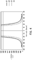
- FIG. 6 is a curve diagram of viewing angle versus luminance ratio of the backlight modules of FIG. 1 and FIG. 3 .
- FIG. 7 is a cross-sectional view of an optical film according to another embodiment of the invention.
- FIG. 8 is a cross-sectional view of an optical film according to yet another embodiment of the invention.
- FIG. 9 is a bottom view of a backlight module in a third embodiment of the invention.
- FIG. 10 is a bottom view of a backlight module in a forth embodiment of the invention.
- FIG. 11 is a bottom view of a backlight module in a fifth embodiment of the invention.
- FIG. 12 is a curve diagram of viewing angle versus luminance ratio of the backlight modules of FIG. 1 , FIG. 3 and FIG. 11 .
- FIG. 13 is a side view of a display apparatus in an embodiment of the invention.
- FIG. 14 is a side view of a display apparatus in another embodiment of the invention.
- FIG. 15 is a side view of a display apparatus in yet another embodiment of the invention.
- FIG. 16 is a side view of a display apparatus in still another embodiment of the invention.
- the description of “A” component facing “B” component herein may contain the situations that “A” component directly faces “B” component or one or more additional components are between “A” component and “B” component.
- the description of “A” component “adjacent to” “B” component herein may contain the situations that “A” component is directly “adjacent to” “B” component or one or more additional components are between “A” component and “B” component. Accordingly, the drawings and descriptions will be regarded as illustrative in nature and not as restrictive.
- FIG. 1 is a schematic diagram of a backlight module in a first embodiment of the invention.
- FIG. 2 is a side view of the backlight module of FIG. 1 .
- a backlight module 10 includes a light guide plate 100 , a light source 110 , a prism sheet 120 and a light absorbing sheet 130 .
- the light guide plate 100 has a light incident surface 100 b , a light emitting surface 100 a connected to the light incident surface 100 b and a bottom surface 100 c opposite to the light emitting surface 100 a .
- the prism sheet 120 is overlapped with the light guide plate 100 , and the prism sheet 120 is disposed on a side of the light emitting surface 100 a of the light guide plate 100 .
- the light source 110 is disposed on a side of the light incident surface 100 b of the light guide plate 100 . That is, the backlight module 10 of the embodiment is an edge type backlight module. It should be noted that in this embodiment, the number of the light sources 110 is exemplarily described by taking four as an example, but the invention is not limited by the disclosure of the drawings. In other embodiments, the number of the light sources 110 may be adjusted according to an optical design of the backlight module.
- the prism sheet 120 includes a substrate 121 and a plurality of prism structures 122 facing the light emitting surface 100 a .
- the substrate 121 has a light incident side 121 a and a light emitting side 121 b opposite to each other.
- the light incident side 121 a faces the light guide plate 100
- the prism structures 122 are disposed on the light incident side 121 a of the substrate 121 .
- materials of the substrate 121 and the prism structures 122 may include polyethylene terephthalate (PET), polycarbonate (PC), UV glue, other suitable polymers, or a combination of the above materials.
- the prism structures 122 of the prism sheet 120 may be arranged on the substrate 121 along a direction X and extending in a direction Y.
- an extending direction of the prism structures 122 is parallel to the light incident surface 100 b of the light guide plate 100 .
- a cross-sectional profile of the prism structure 122 on a plane (i.e., an XZ plane) perpendicular to the extending direction (i.e., the direction Y) may be a triangle. That is, the prism structures 122 of this embodiment may be triangular prism strips, but the invention is not limited thereto.
- each of the prism structures 122 has a first inclined surface 122 s 1 and a second inclined surface 122 s 2 opposite to each other.
- a ridge line RL 1 of the prism structure 122 is defined at a junction of the first inclined surface 122 s 1 and the second inclined surface 122 s 2 , and the ridge line RL 1 may extend in the direction Y.
- a first vertex angle ⁇ 1 is provided between the first inclined surface 122 s 1 and the second inclined surface 122 s 2 of the prism structure 122 , and the first vertex angle ⁇ 1 of the prism structure 122 may fall between 60 degrees and 75 degrees.
- the invention is not limited in this regard.
- a light emitting brightness of the backlight module 10 near the normal viewing angle e.g., a viewing angle range between ⁇ 15 degrees and 15 degrees
- a light emitting brightness of a backlight module provided without the prism sheet 120 is higher than a light emitting brightness of a backlight module provided without the prism sheet 120 .
- the light guide plate 100 has a plurality of micro lens structures 100 m 1 and a plurality of micro lens structures 100 m 2 , and the micro lens structures 100 m 1 and the micro lens structures 100 m 2 are disposed on the light emitting surface 100 a and the bottom surface 100 c of the light guide plate 100 , respectively.
- the invention is not limited in this regard.
- the micro lens structures may also be disposed on only one of the light emitting surface and the bottom surface of the light guide plate according to the actual light type requirements.
- the micro lens structures 100 m 1 of the light guide plate 100 are arranged on the light emitting surface 100 a along the direction Y, and an extending direction of the micro lens structures 100 m 1 is perpendicular to the light incident surface 100 b of the light guide plate 100 (i.e., the direction X).
- the micro lens structures 100 m 2 of the light guide plate 100 are arranged on the bottom surface 100 c along the direction X, and an extending direction of the micro lens structures 100 m 2 is parallel to the light incident surface 100 b of the light guide plate 100 (i.e., the direction Y).
- the extending direction of the micro lens structures 100 m 1 may be perpendicular to the extending direction of the micro lens structures 100 m 2 , but the invention is not limited thereto. According to other embodiments, depending on the actual light type requirements, the extending direction of the micro lens structures 100 m 1 of the light guide plate 100 may not be perpendicular to the light incident surface 100 b of the light guide plate 100 but intersected with the extending direction of the micro lens structures 100 m 2 .
- a cross-sectional profile of the micro lens structure 100 m 1 of the light guide plate 100 on a plane (i.e., a YZ plane) perpendicular to the extending direction (i.e., the direction X) may be a semi-oval shape. That is, the micro lens structures 100 m 1 of this embodiment may be rod lens strips, but the invention is not limited thereto. In other embodiments, the cross-sectional profile of the micro lens structure 100 m 1 on the plane perpendicular to the extending direction may also be adjusted according to actual light type requirements (or light splitting effect).
- a cross-sectional profile of the micro lens structure 100 m 2 of the light guide plate 100 on a plane (i.e., an XZ plane) perpendicular to the extending direction (i.e., the direction Y) may be a wedge. That is, the micro lens structures 100 m 2 may be (inclined) triangular lens strips, but the invention is not limited thereto. In other embodiments, the cross-sectional profile of the micro lens structures 100 m 2 on the plane perpendicular to the extending direction may also be adjusted according to actual light type requirements (or light splitting effect).
- the number of the micro lens structures of the light guide plate 100 in this embodiment is only for illustrative purposes, and is not intended to limit the invention. In other embodiments, the number of the micro lens structures of the light guide plate may also adjusted according to actual design requirements (e.g., the configuration relationship with the light source or the size of the light guide plate).
- the light absorbing sheet 130 of the backlight module 10 is disposed on a side of the bottom surface 100 c of the light guide plate 100 .
- most of the light beam emitted by the light source 110 may be emitted from the light emitting surface 100 a and focused near the normal viewing angle (e.g., the viewing angle range between ⁇ 15 degrees and 15 degrees; total viewing angle range of about 30 degrees).
- a part of the light beam may be emitted from the bottom surface 100 c , and reflected again (e.g., reflected by backplate, mirror reflection sheet, or frame) to the light emitting surface 100 a to be emitted.
- the unexpected light beam emitted from the bottom surface 100 c may be effectively absorbed.
- the influence of the stray light on the light output type of the backlight module may be effectively reduced so as to further improve a light collection of the backlight module.
- the absorption of the light absorbing sheet 130 within the wavelength range of visible light may selectively be higher than 90%.
- FIG. 3 is a schematic diagram of a backlight module in a second embodiment of the invention.
- FIG. 4 is a side view of the backlight module of FIG. 3 .
- FIG. 5 is a bottom view of the backlight module of FIG. 3 .
- the major difference between a backlight module 11 of this embodiment and the backlight module 10 of FIG. 1 is the different composition of the backlight module.
- the backlight module 11 of this embodiment further includes an optical film 140 disposed between the light guide plate 100 and the light absorbing sheet 130 .
- the optical film 140 includes a substrate 141 and a plurality of optical micro structures 142 facing the light absorbing sheet 130 .
- the substrate 141 includes a first side 141 a and a second side 141 b opposite to each other.
- the first side 141 a faces the light absorbing sheet 130
- the optical micro structures 142 are disposed on the first side 141 a of the substrate 141 .
- materials of the substrate 141 and the optical micro structure 142 may include polyethylene terephthalate (PET), polycarbonate (PC), UV glue, other suitable polymers, or a combination of the above materials.
- the optical micro structures 142 of the optical film 140 may be arranged on the first side 141 a of the substrate 141 along the direction Y, and an extending direction of the optical micro structures 142 may selectively be perpendicular to the light incident surface 100 b of the light guide plate 100 .
- FIG. 5 only illustrates the light guide plate 100 , the light source 110 and the optical micro structures 142 of the optical film 140 of FIG. 3 .
- the invention is not limited in this regard. According to other embodiments, it is also possible that the extending direction of the optical micro structures 142 is not perpendicular to the light incident surface 100 b of the light guide plate 100 .
- a cross-sectional profile of optical micro structure 142 on a plane (i.e., the YZ plane) perpendicular to the extending direction (i.e., the direction X) may be a triangle. That is, the optical micro structures 142 of the present embodiment may be triangular prism strips.
- each of the optical micro structures 142 has a first inclined surface 142 s 1 and a second inclined surface 142 s 2 opposite to each other.
- a ridge line RL 2 is defined at a junction of the first inclined surface 142 s 1 and the second inclined surface 142 s 2 of the optical micro structure 142 , and the ridge line RL 2 may extend in the direction X. That is, a cross-sectional profile of optical micro structures 142 on a plane (i.e., the YZ plane) perpendicular to the extending direction may be a triangle.
- the invention is not limited in this regard.
- the cross-sectional profile of the optical micro structure 142 on the plane perpendicular to the extending direction may also be adjusted according to actual light type requirements (or light splitting effect).
- a second vertex angle ⁇ 2 is provided between the first inclined surface 142 s 1 and the second inclined surface 142 s 2 of the optical micro structure 142 , and the second vertex angle ⁇ 2 of the optical micro structure 142 may fall between 80 degrees and 140 degrees.
- the invention is not limited in this regard.
- the light hits the optical micro structure 142 of the optical film 140 , if a projection of a travelling direction of the light on the light emitting surface 100 a is parallel to a projection of the ridge line RL 2 on the light emitting surface 100 a or there is a small angle included in between the two, the light is reflected by the optical micro structure 142 and transmitted towards the light emitting surface 100 a ; otherwise, the light penetrates the optical micro structure 142 and is absorbed by the light absorbing sheet 130 . In this way, a proportion of the light being reflected and transmitted by the optical micro structure 142 may be controlled by designing the cross-sectional profile of the optical micro structure 142 or the direction of the ridge line RL 2 .
- FIG. 6 is a graph of the viewing angle versus luminance ratio of the four backlight modules of FIG. 1 and FIG. 3 , where a curve C 1 , a curve C 2 , a curve C 3 and a curve C 4 respectively show changes in the luminance ratio of the four backlight modules at different viewing angles.
- the curve C 1 corresponds to a backlight module provided without the light absorbing sheet 130 and the optical film 140 ;
- the curve C 2 corresponds to the backlight module 10 provided with the light absorbing sheet 130 but without the optical film 140 ;
- the curve C 3 corresponds to the backlight module 11 provided with the light absorbing sheet 130 and the optical film 140 having the second vertex angle ⁇ 2 of the optical micro structure 142 being 90 degrees;
- the curve C 4 corresponds to the backlight module 11 provided with the light absorbing sheet 130 and the optical film 140 having the second vertex angle ⁇ 2 of the optical micro structure 142 being 140 degrees.
- the luminance ratio herein is a ratio of the light emitting brightness of each backlight module at each viewing angle to the light emitting brightness of each backlight module at the normal viewing angle (i.e., when the viewing angle is 0 degree, for example, normalized to 1).
- the backlight module provided without the light absorbing sheet 130 is, for example, a backlight module with a mirror reflection sheet disposed on a side of the bottom surface of the light guide such as the 3M product called ESR (Enhanced Specular Reflector).
- the light emitting luminance ratios of the backlight module 11 at the viewing angle of 45 degrees are lower than the light emitting luminance ratio of the backlight module provided without the light absorbing sheet 130 (as shown by the curve C 1 ).
- the light emitting luminance ratios of the backlight module 11 at the viewing angle of 45 degrees are higher than the light emitting luminance ratio of the backlight module 10 provided with the light absorbing sheet 130 but without the optical film 140 (as shown by the curve C 2 ). Therefore, as can be learnt from FIG. 6 that under the architecture of the backlight module 11 of FIG. 3 , with the light emitting luminance ratio and a maximum brightness taken into consideration, if an optimal design value of the second vertex angle ⁇ 2 of the optical micro structure 142 is 90 degrees, the anti-peep effect may be better than a common backlight module and the backlight module 10 .
- the viewing angle (e.g. the viewing angle of 45 degrees) selected for determining the optimal design value of the second vertex angle ⁇ 2 is determined according to an optical specification (i.e., inspection item) of an anti-peep display apparatus.
- the viewing angle selected for determining the optimal design value of the second vertex angle ⁇ 2 may also be adjusted according to use of the backlight module.
- FIG. 7 is a cross-sectional view of an optical film according to another embodiment of the invention.
- FIG. 8 is a cross-sectional view of an optical film according to yet another embodiment of the invention.
- the difference between an optical film 140 A (as shown in FIG. 7 ), an optical film 140 B (as shown in FIG. 8 ) and the optical film 140 (as shown in FIG. 4 ) is the configuration of the optical micro structures, Specifically, each of the optical micro structures of the optical films 140 , 140 A and 140 B has one vertex angle.
- a cross-sectional profile of an optical micro structure 142 A of the optical film 140 A on the YZ plane is a combination of multiple straight line segments 1421 (i.e., polylines).
- a cross-sectional profile of an optical micro structure 142 B of the optical film 140 B of the YZ plane is a combination of a straight line segment 1421 and an arc segment 1422 .
- the invention is not limited in this regard.
- the cross-sectional profile of the optical micro structure of the optical film on the YZ plane may also be adjusted according to different optical design requirements.
- FIG. 9 is a bottom view of a backlight module in a third embodiment of the invention.
- FIG. 10 is a bottom view of a backlight module in a forth embodiment of the invention.
- FIG. 9 and FIG. 10 only illustrate the light guide plate 100 , the light source 110 , optical micro structures 142 C of an optical film 140 C, and optical micro structures 142 D of an optical film 140 D.
- the difference between a backlight module 11 A of this embodiment and the backlight module 11 of FIG. 5 is the extending direction of the optical micro structures.
- a normal projection of a ridge line RL 2 -A of the optical micro structure 142 C of the optical film 140 C (i.e., an extending path) on the light emitting surface 100 a of the light guide surface 100 is not perpendicular to the light incident surface 100 b of the light guide plate 100 .
- an included angle ⁇ is provided between the extending direction of the optical micro structure 142 C (or the ridge line RL 2 -A) and the light incident surface 100 b of the light guide plate 100 , and the included angle ⁇ is between 75 degrees and 105 degrees. Accordingly, the bright and dark lines (i.e., the moiré pattern) produced between the optical film 140 C and the micro lens structures 100 m 1 (as shown in FIG. 3 ) of the light guide plate 100 may be effectively suppressed. In other words, a light output uniformity of the backlight module 11 A may be improved.
- the difference between a backlight module 11 B of this embodiment, the backlight module 11 of FIG. 5 and the backlight module 11 A of FIG. 9 is the different configuration of the optical micro structures.
- a normal projection of a ridge line RL 2 -B of the optical micro structure 142 D of the optical film 140 D (i.e., the extending path) on the light emitting surface 100 a of the light guide surface 100 is wavy.
- the extending path of the optical microstructure 142 D is wavy, the normal projection of the ridge line RL 2 -B on the light guide plate 100 is still limited between two virtual straight lines IL, and an extending direction of the two virtual straight lines IL are still substantially identical to the extending direction of the optical micro structures 142 C of FIG. 9 .
- an included angle between the virtual straight line IL and the light incident surface 100 b of the light guide plate 100 may fall between, for example, 75 degrees and 105 degrees.
- the optical micro structure 142 D may be effectively suppressed.
- a light output uniformity of the backlight module 11 B may be improved.
- the optical micro structures 142 D with a wavy structure may also suppress the bright and dark lines (i.e., mura) produced between the optical film 140 D and the display panel.
- FIG. 11 is a bottom view of a backlight module in a fifth embodiment of the invention.
- the difference between a backlight module 12 of this embodiment and the backlight module 11 in FIG. 4 is the different type of the optical film.
- an optical film 145 disposed between the light absorbing sheet 130 and the light guide plate 100 is, for example, a reflective polarizer.
- An included angel between a reflection axis RA of the reflective polarizer (i.e., the optical film 145 ) and the light incident surface 100 b of the light guide plate 100 may fall between 70 degrees and 110 degrees, and more preferably, at 90 degrees.
- the invention is not limited in this regard.
- this reflective polarizer i.e., the optical film 145
- this reflective polarizer may have a higher reflectance for a light beam with a traveling direction substantially parallel to the reflection axis RA, and have a lower reflectance for a light beam with a traveling direction substantially perpendicular to the reflection axis RA.
- This reflective polarizer has a lowest reflectance (viewing angle) at an oblique viewing angle in a range of 50 degrees to 60 degrees.
- the invention is not limited in this regard.
- a reflectance distribution of the reflective polarizer for different viewing angles may also be adjusted according to the actual light type requirements.
- FIG. 12 is a graph of the viewing angle versus luminance ratio of the three backlight modules of FIG. 1 , FIG. 3 and FIG. 11 , where a curve C 5 , a curve C 6 and a curve C 7 respectively show changes in the luminance ratio of the three backlight modules at different viewing angles.
- the curve C 5 corresponds to the backlight module 12 provided with the light absorbing sheet 130 and the optical film 145 ;
- the curve C 6 corresponds to the backlight module 11 provided with the light absorbing sheet 130 and the optical film 140 having the second vertex angle ⁇ 2 of the optical micro structure 142 being 90 degrees;
- the curve C 7 corresponds to the backlight module 10 provided with the light absorbing sheet 130 but without the optical film 140 .
- the luminance ratio herein is a ratio of the light emitting brightness of each backlight module at each viewing angle to the light emitting brightness of each backlight module at the normal viewing angle.
- the optical film 145 e.g., the reflective polarizer
- the light emitting luminance ratio of the backlight module 12 near the viewing angle of 45 degrees is clearly lower than the light emitting luminance ratio of the backlight module 11 near the viewing angle of 45 degrees (as shown by the curve C 6 ).
- the light output of the backlight module at the oblique viewing angle may be reduced to improve the anti-peep effect.
- a light output loss of the backlight module near the normal viewing angle e.g., the viewing angle range of ⁇ 15 degrees to 15 degrees
- the light collection of the backlight module may be improved accordingly.
- FIG. 13 is a side view of a display apparatus in an embodiment of the invention.
- a display apparatus 1 may include the backlight module 10 , a display panel 200 and an electrically controlled diffusion film 300 .
- the display panel 200 and the electrically controlled diffusion film 300 are overlapped with the light emitting surface 100 a of the light guide plate 100 .
- the electrically controlled diffusion film 300 is overlapped with the display panel 200 and located between the display panel 200 and the backlight module 10 .
- the display apparatus 1 of this embodiment can provide a switchable anti-peep function.
- the disclosure is not limited in this regard. In other embodiments, it is also possible that the display apparatus does not have the electrically controlled diffusion film 300 .
- the display apparatus can provide the anti-peep effect compared to the general displays but cannot provide the effect of switching between a sharing mode and an anti-peep mode.
- the display panel 200 is, for example, a liquid crystal display (LCD) panel, an electrophoretic display (EPD) panel or other non self-emissive display panels.
- the electrically controlled diffusion film 300 is, for example, a polymer dispersed liquid crystal (PDLC) film, a polymer network liquid crystal (PNLC) film, a liquid crystal lens (LC Lens), or other structures that can change the degree of light beam divergence by electrical control.
- the display apparatus 1 may adjust a light pattern of the light beam emitted from the backlight module 10 through the electrically controlled diffusion film 300 .
- the light beam emitted from the backlight module 10 at a small angle e.g., narrow light beam angle
- a large angle e.g., wide light beam angle
- the electrically controlled diffusion film 300 may be disabled so the purpose of the anti-peep can be achieved through the better light collection of the backlight module 10 .
- the invention is not limited in this regard.
- FIG. 14 is a side view of a display apparatus in another embodiment of the invention.
- a display apparatus 2 may include the backlight module 11 , the display panel 200 and an electrically controlled viewing angle switch 310 .
- the electrically controlled viewing angle switch 310 is overlapped with the display panel 200 . More specifically, the display apparatus 2 of this embodiment may also provide the switchable anti-peep function. However, the disclosure is not limited in this regard. In other embodiments, it is also possible that the display apparatus does not have the electrically controlled viewing angle switch 310 .
- the electrically controlled viewing angle switch 310 may be selectively disposed between the display panel 200 and the prism sheet 120 , but the invention is not limited thereto.
- the display panel 200 may also be disposed between the electrically controlled viewing angle switch 310 and the prism sheet 120 .
- the electrically controlled viewing angle switch 310 may include a liquid crystal cell (not illustrated) and two polarizers (not illustrated) disposed on two opposite sides of the liquid crystal cell.
- the liquid crystal cell includes a liquid crystal layer (not illustrated) and two electrode layers (not illustrated) located on two opposite sides of the liquid crystal layer.
- the two electrode layers may be enabled to form an electric field between the two electrode layers.
- the electric field is configured to drive a plurality of liquid crystal molecules (not illustrated) of the liquid crystal layers to rotate. Accordingly, optical axes of the liquid crystal molecules may be changed according to different electric field sizes and distributions so that the light output of the electrically controlled viewing angle switch 310 at different viewing angles may be adjusted.
- the electrically controlled viewing angle switch 310 has a viewing angle control direction (e.g., the direction Y) perpendicular to an axial direction of optical axes of the liquid crystal molecules, and the display apparatus 2 may electronically control and switch the total light output of a large viewing angle range in this viewing angle control direction.
- the total light output of the large viewing angle range may be significantly reduced (or suppressed).
- the sharing mode the total light output of the large viewing angle range may be restored.
- the backlight module 11 of this embodiment may improve the total light output of the display apparatus 2 near the normal viewing angle through the better light collection.
- the display apparatus 2 may be switched to the anti-peep mode or the sharing mode.
- the backlight module 11 may provide a more preferable anti-peep effect for the display apparatus 2 .
- FIG. 15 is a side view of a display apparatus in yet another embodiment of the invention.
- the major difference between a display apparatus 3 of this embodiment and the display apparatus 2 of FIG. 14 is the different composition of the backlight module.
- the electrically controlled viewing angle switch 310 may include a liquid crystal cell 311 and a polarizer 312 and a polarizer 313 disposed on two opposite sides of the liquid crystal cell 311 .
- the liquid crystal cell 311 includes a liquid crystal layer (not illustrated) and two electrode layers (not illustrated) located on two opposite sides of the liquid crystal layer. The two electrode layers may be enabled to form an electric field between the two electrode layers.
- the electric field is configured to drive a plurality of liquid crystal molecules (not illustrated) of the liquid crystal layers to rotate. Accordingly, optical axes of the liquid crystal molecules may be changed according to different electric field sizes and distributions so that the light output of the electrically controlled viewing angle switch 310 at different viewing angles may be adjusted.
- the polarizer 312 is located between the liquid crystal cell 311 and the prism sheet 120
- the polarizer 313 is located between the liquid crystal cell 311 and the display panel 200 . Because the reflection axis RA of the optical film 145 (e.g., the reflective polarizer) of the backlight module 12 of the display apparatus 3 is perpendicular to the light incident surface 100 b of the light guide plate 100 , a penetration axis TA of the polarizer 312 of the electrically controlled viewing angle switch 310 also needs to be perpendicular to the light incident surface 100 b of the light guide plate 100 (that is, the penetration axis TA of the polarizer 312 is parallel to the reflection axis RA of the optical film 145 ) so that the light energy utilization of the display apparatus 3 may be maximized.
- the reflection axis RA of the optical film 145 e.g., the reflective polarizer
- the backlight module 12 of the present embodiment may improve the total light output of the display apparatus 3 near the normal viewing angle through the better light collection. Further, in cooperation with the electrically controlled viewing angle switch 310 to improve the anti-peep effect, the display apparatus 3 may be switched to the anti-peep mode or the sharing mode. In other words, the backlight module 12 may provide a more preferable anti-peep effect for the display apparatus 3 .
- FIG. 16 is a side view of a display apparatus in still another embodiment of the invention.
- the difference between a display apparatus 4 of this embodiment and the display apparatus 3 of FIG. 15 is the different composition of the backlight module and the different axial direction of the penetration axis TA of the polarizer.
- the reflection axis RA of the optical film 145 (e.g., the reflective polarizer) of a backlight module 12 A of the display apparatus 4 is perpendicular to the light incident surface 100 b of the light guide plate 100 .
- a penetration axis TA of a polarizer 312 A of the electrically controlled viewing angle switch 310 is parallel to the light incident surface 100 b of the light guide plate 100 . Therefore, the backlight module 12 A further includes a half wave plate 150 , and the half wave plate 150 is disposed between the polarizer 312 A and the prism sheet 120 .
- the light beam emitted from the light emitting surface 121 b of the prism sheet 120 and passed through the half wave plate 150 can have a polarization direction parallel to the axial direction of the penetration axis TA of the polarizer 312 A so that the light energy utilization of the display apparatus 4 may be maximized.
- the backlight module 12 A of the present embodiment may improve the total light output of the display apparatus 4 near the normal viewing angle through the better light collection. In other words, the backlight module 12 A may provide a more preferable anti-peep effect for the display apparatus 4 .
- the backlight module in the backlight module according to an embodiment of the invention, with the light absorbing sheet disposed on one side of the bottom surface of the light guide plate and the absorption of the light absorbing sheet within the wavelength range of visible light higher than 70%, the influence of the stray light on the light output type of the backlight module may be effectively suppressed to improve the light collection of the backlight module.
- the light output of the display apparatus using the backlight module in the side view angle can be effectively reduced, thereby improving the anti-peep performance of the display apparatus.
- the term “the invention”, “the present invention” or the like does not necessarily limit the claim scope to a specific embodiment, and the reference to particularly preferred exemplary embodiments of the invention does not imply a limitation on the invention, and no such limitation is to be inferred.
- the invention is limited only by the spirit and scope of the appended claims. Moreover, these claims may refer to use “first”, “second”, etc. following with noun or element. Such terms should be understood as a nomenclature and should not be construed as giving the limitation on the number of the elements modified by such nomenclature unless specific number has been given.
- the abstract of the disclosure is provided to comply with the rules requiring an abstract, which will allow a searcher to quickly ascertain the subject matter of the technical disclosure of any patent issued from this disclosure.
Abstract
Description
Claims (6)
Applications Claiming Priority (2)
| Application Number | Priority Date | Filing Date | Title |
|---|---|---|---|
| CN201911263904.2 | 2019-12-11 | ||
| CN201911263904.2A CN112946951A (en) | 2019-12-11 | 2019-12-11 | Backlight module and display device |
Publications (2)
| Publication Number | Publication Date |
|---|---|
| US20210181580A1 US20210181580A1 (en) | 2021-06-17 |
| US11391987B2 true US11391987B2 (en) | 2022-07-19 |
Family
ID=75745604
Family Applications (1)
| Application Number | Title | Priority Date | Filing Date |
|---|---|---|---|
| US17/111,433 Active US11391987B2 (en) | 2019-12-11 | 2020-12-03 | Backlight module and display apparatus |
Country Status (3)
| Country | Link |
|---|---|
| US (1) | US11391987B2 (en) |
| CN (1) | CN112946951A (en) |
| TW (1) | TWI718820B (en) |
Families Citing this family (4)
| Publication number | Priority date | Publication date | Assignee | Title |
|---|---|---|---|---|
| CN111487708B (en) * | 2020-04-24 | 2022-07-05 | 京东方科技集团股份有限公司 | Side-in backlight module and liquid crystal display device |
| CN112859435A (en) * | 2021-01-12 | 2021-05-28 | 扬昕科技(苏州)有限公司 | Light guide plate and light source module |
| CN113204141A (en) * | 2021-04-28 | 2021-08-03 | 京东方科技集团股份有限公司 | Backlight module and display device |
| WO2023279224A1 (en) * | 2021-07-05 | 2023-01-12 | 瑞仪光电(苏州)有限公司 | Backlight module and display apparatus |
Citations (15)
| Publication number | Priority date | Publication date | Assignee | Title |
|---|---|---|---|---|
| US5557433A (en) * | 1994-02-28 | 1996-09-17 | Nec Corporation | Transmissive liquid crystal display having prism lens film for light illumination and wave lens film for light diffusion |
| JPH10206849A (en) | 1997-01-27 | 1998-08-07 | Seiko Epson Corp | Liquid crystal display device and electronic equipment using the same |
| US20040042233A1 (en) * | 2002-08-30 | 2004-03-04 | Fujitsu Display Technologies Corporation | Lighting unit and display device |
| US20090180191A1 (en) * | 2006-04-28 | 2009-07-16 | Yukinori Yamada | Lens sheet for use in backlight, backlight and display device using the same |
| US7784954B1 (en) * | 2006-07-25 | 2010-08-31 | Fusion Optix, Inc. | Polarization sensitive light homogenizer |
| US20110025946A1 (en) * | 2006-06-09 | 2011-02-03 | Ubright Optronics Corporation | Luminance enhancement optical substrates with anti-interference-fringe structures |
| US20110051022A1 (en) * | 2009-08-25 | 2011-03-03 | Samsung Electronics Co., Ltd. | Backlight assembly and display device having the same |
| US20120086332A1 (en) * | 2009-06-25 | 2012-04-12 | Panasonic Corporation | Multicolor light-emitting organic el display device and method of manufacturing multicolor light-emitting organic el display device |
| US20120105771A1 (en) * | 2010-10-29 | 2012-05-03 | Hitachi Displays, Ltd. | Liquid crystal display device |
| US20140320784A1 (en) * | 2013-04-30 | 2014-10-30 | Lg Display Co., Ltd. | Display device |
| US8982300B2 (en) | 2007-12-17 | 2015-03-17 | Nitto Denko Corporation | Viewing angle controlling system, and image display device using the same |
| TWI592722B (en) | 2016-03-16 | 2017-07-21 | 揚昇照明股份有限公司 | Backlight module and display apparatus |
| EP3355105A1 (en) | 2017-01-25 | 2018-08-01 | Young Lighting Technology Inc. | Viewing angle switchable display apparatus |
| CN109212660A (en) | 2018-10-26 | 2019-01-15 | 合肥京东方光电科技有限公司 | Leaded light component, light collimator assembly, backlight module and display device |
| US20190369319A1 (en) * | 2018-05-31 | 2019-12-05 | Stanley Electric Co., Ltd. | Side-edge type surface light emitting apparatus having light guide plate sandwiched by upper and lower prism sheets |
Family Cites Families (8)
| Publication number | Priority date | Publication date | Assignee | Title |
|---|---|---|---|---|
| CN100426011C (en) * | 2003-03-03 | 2008-10-15 | 三菱丽阳株式会社 | Optical deflector element and light source device |
| US20050271348A1 (en) * | 2004-06-02 | 2005-12-08 | Hsin-Hsin Huang Hsu | Prism sheet for a backlight module |
| CN1710478A (en) * | 2005-07-05 | 2005-12-21 | 友达光电股份有限公司 | Light-guide plate with bent groove |
| US20070223249A1 (en) * | 2006-03-24 | 2007-09-27 | Eastman Kodak Company | Light redirecting film |
| TW200736754A (en) * | 2006-03-31 | 2007-10-01 | Gamma Optical Co Ltd | Optical film for edge-type backlight module |
| CN107111184A (en) * | 2014-12-23 | 2017-08-29 | 3M创新有限公司 | Reflector layer is fit |
| CN207650518U (en) * | 2017-12-26 | 2018-07-24 | 扬升照明股份有限公司 | Display module can be switched in visual angle switchable apparatus and visual angle |
| CN110546647B (en) * | 2018-07-25 | 2021-01-01 | 深圳市汇顶科技股份有限公司 | Optical fingerprint sensor under screen based on utilize off-axis pinhole to carry out lens-pinhole formation of image |
-
2019
- 2019-12-11 CN CN201911263904.2A patent/CN112946951A/en active Pending
- 2019-12-19 TW TW108146784A patent/TWI718820B/en active
-
2020
- 2020-12-03 US US17/111,433 patent/US11391987B2/en active Active
Patent Citations (15)
| Publication number | Priority date | Publication date | Assignee | Title |
|---|---|---|---|---|
| US5557433A (en) * | 1994-02-28 | 1996-09-17 | Nec Corporation | Transmissive liquid crystal display having prism lens film for light illumination and wave lens film for light diffusion |
| JPH10206849A (en) | 1997-01-27 | 1998-08-07 | Seiko Epson Corp | Liquid crystal display device and electronic equipment using the same |
| US20040042233A1 (en) * | 2002-08-30 | 2004-03-04 | Fujitsu Display Technologies Corporation | Lighting unit and display device |
| US20090180191A1 (en) * | 2006-04-28 | 2009-07-16 | Yukinori Yamada | Lens sheet for use in backlight, backlight and display device using the same |
| US20110025946A1 (en) * | 2006-06-09 | 2011-02-03 | Ubright Optronics Corporation | Luminance enhancement optical substrates with anti-interference-fringe structures |
| US7784954B1 (en) * | 2006-07-25 | 2010-08-31 | Fusion Optix, Inc. | Polarization sensitive light homogenizer |
| US8982300B2 (en) | 2007-12-17 | 2015-03-17 | Nitto Denko Corporation | Viewing angle controlling system, and image display device using the same |
| US20120086332A1 (en) * | 2009-06-25 | 2012-04-12 | Panasonic Corporation | Multicolor light-emitting organic el display device and method of manufacturing multicolor light-emitting organic el display device |
| US20110051022A1 (en) * | 2009-08-25 | 2011-03-03 | Samsung Electronics Co., Ltd. | Backlight assembly and display device having the same |
| US20120105771A1 (en) * | 2010-10-29 | 2012-05-03 | Hitachi Displays, Ltd. | Liquid crystal display device |
| US20140320784A1 (en) * | 2013-04-30 | 2014-10-30 | Lg Display Co., Ltd. | Display device |
| TWI592722B (en) | 2016-03-16 | 2017-07-21 | 揚昇照明股份有限公司 | Backlight module and display apparatus |
| EP3355105A1 (en) | 2017-01-25 | 2018-08-01 | Young Lighting Technology Inc. | Viewing angle switchable display apparatus |
| US20190369319A1 (en) * | 2018-05-31 | 2019-12-05 | Stanley Electric Co., Ltd. | Side-edge type surface light emitting apparatus having light guide plate sandwiched by upper and lower prism sheets |
| CN109212660A (en) | 2018-10-26 | 2019-01-15 | 合肥京东方光电科技有限公司 | Leaded light component, light collimator assembly, backlight module and display device |
Also Published As
| Publication number | Publication date |
|---|---|
| US20210181580A1 (en) | 2021-06-17 |
| CN112946951A (en) | 2021-06-11 |
| TW202122891A (en) | 2021-06-16 |
| TWI718820B (en) | 2021-02-11 |
Similar Documents
| Publication | Publication Date | Title |
|---|---|---|
| US11391987B2 (en) | Backlight module and display apparatus | |
| US11029462B2 (en) | Backlight module having an optical film and display apparatus having the same | |
| TWI444715B (en) | Liquid crystal display | |
| CN104246590B (en) | Liquid crystal display | |
| TWI659247B (en) | Liquid crystal display device | |
| CN114341681A (en) | Optical stack for privacy display | |
| KR20020001594A (en) | Light pipe, plane light source unit and reflection type liquid-crystal display device | |
| US11402692B2 (en) | Backlight module having an optical film and display apparatus having the same | |
| KR20110019388A (en) | Hollow backlight with tilted light source | |
| CN101535878A (en) | Back-lit displays with high illumination uniformity | |
| JP2002023155A (en) | Reflective liquid crystal display device | |
| US20120113357A1 (en) | Transmissive Liquid Crystal Display with Reflective Mode | |
| US11150399B2 (en) | Backlight module and display apparatus | |
| US11016337B2 (en) | Light source module and dual display device | |
| JP2010262813A (en) | Lighting device, and liquid crystal display device | |
| JP2001051268A (en) | Liquid crystal display device | |
| US11828974B2 (en) | Backlight module and display apparatus | |
| RU2454689C2 (en) | Backlight module and liquid crystal display | |
| US20220244598A1 (en) | Display device | |
| US11698553B2 (en) | Backlight module and display apparatus | |
| CN217332919U (en) | Backlight module with optical film and display device | |
| US11947217B2 (en) | Backlight module and display apparatus | |
| US20240036429A1 (en) | Electrically controlled optical screen | |
| US20230288753A1 (en) | Backlight module and display apparatus | |
| JP7361683B2 (en) | liquid crystal display device |
Legal Events
| Date | Code | Title | Description |
|---|---|---|---|
| FEPP | Fee payment procedure |
Free format text: ENTITY STATUS SET TO UNDISCOUNTED (ORIGINAL EVENT CODE: BIG.); ENTITY STATUS OF PATENT OWNER: LARGE ENTITY |
|
| AS | Assignment |
Owner name: CORETRONIC CORPORATION, TAIWAN Free format text: ASSIGNMENT OF ASSIGNORS INTEREST;ASSIGNORS:CHEN, PING-YEN;FANG, CHUNG-YANG;LIN, YANG-CHING;AND OTHERS;REEL/FRAME:054584/0554 Effective date: 20201202 |
|
| STPP | Information on status: patent application and granting procedure in general |
Free format text: RESPONSE TO NON-FINAL OFFICE ACTION ENTERED AND FORWARDED TO EXAMINER |
|
| STPP | Information on status: patent application and granting procedure in general |
Free format text: FINAL REJECTION MAILED |
|
| STPP | Information on status: patent application and granting procedure in general |
Free format text: NON FINAL ACTION MAILED |
|
| STPP | Information on status: patent application and granting procedure in general |
Free format text: RESPONSE TO NON-FINAL OFFICE ACTION ENTERED AND FORWARDED TO EXAMINER |
|
| STPP | Information on status: patent application and granting procedure in general |
Free format text: NOTICE OF ALLOWANCE MAILED -- APPLICATION RECEIVED IN OFFICE OF PUBLICATIONS |
|
| STPP | Information on status: patent application and granting procedure in general |
Free format text: PUBLICATIONS -- ISSUE FEE PAYMENT VERIFIED |
|
| STCF | Information on status: patent grant |
Free format text: PATENTED CASE |