EP3355040A1 - Electronic component assembly with leads and manufacturing method therefor - Google Patents
Electronic component assembly with leads and manufacturing method therefor Download PDFInfo
- Publication number
- EP3355040A1 EP3355040A1 EP16847882.4A EP16847882A EP3355040A1 EP 3355040 A1 EP3355040 A1 EP 3355040A1 EP 16847882 A EP16847882 A EP 16847882A EP 3355040 A1 EP3355040 A1 EP 3355040A1
- Authority
- EP
- European Patent Office
- Prior art keywords
- leads
- electronic component
- metal wire
- lead
- wire exposed
- Prior art date
- Legal status (The legal status is an assumption and is not a legal conclusion. Google has not performed a legal analysis and makes no representation as to the accuracy of the status listed.)
- Granted
Links
Images






Classifications
-
- H—ELECTRICITY
- H01—ELECTRIC ELEMENTS
- H01C—RESISTORS
- H01C17/00—Apparatus or processes specially adapted for manufacturing resistors
- H01C17/28—Apparatus or processes specially adapted for manufacturing resistors adapted for applying terminals
-
- G—PHYSICS
- G01—MEASURING; TESTING
- G01K—MEASURING TEMPERATURE; MEASURING QUANTITY OF HEAT; THERMALLY-SENSITIVE ELEMENTS NOT OTHERWISE PROVIDED FOR
- G01K7/00—Measuring temperature based on the use of electric or magnetic elements directly sensitive to heat ; Power supply therefor, e.g. using thermoelectric elements
- G01K7/16—Measuring temperature based on the use of electric or magnetic elements directly sensitive to heat ; Power supply therefor, e.g. using thermoelectric elements using resistive elements
- G01K7/22—Measuring temperature based on the use of electric or magnetic elements directly sensitive to heat ; Power supply therefor, e.g. using thermoelectric elements using resistive elements the element being a non-linear resistance, e.g. thermistor
- G01K7/223—Measuring temperature based on the use of electric or magnetic elements directly sensitive to heat ; Power supply therefor, e.g. using thermoelectric elements using resistive elements the element being a non-linear resistance, e.g. thermistor characterised by the shape of the resistive element
-
- H—ELECTRICITY
- H01—ELECTRIC ELEMENTS
- H01C—RESISTORS
- H01C1/00—Details
- H01C1/14—Terminals or tapping points specially adapted for resistors; Arrangements of terminals or tapping points on resistors
- H01C1/144—Terminals or tapping points specially adapted for resistors; Arrangements of terminals or tapping points on resistors the terminals or tapping points being welded or soldered
-
- H—ELECTRICITY
- H01—ELECTRIC ELEMENTS
- H01C—RESISTORS
- H01C7/00—Non-adjustable resistors formed as one or more layers or coatings; Non-adjustable resistors made from powdered conducting material or powdered semi-conducting material with or without insulating material
- H01C7/18—Non-adjustable resistors formed as one or more layers or coatings; Non-adjustable resistors made from powdered conducting material or powdered semi-conducting material with or without insulating material comprising a plurality of layers stacked between terminals
-
- H—ELECTRICITY
- H01—ELECTRIC ELEMENTS
- H01G—CAPACITORS; CAPACITORS, RECTIFIERS, DETECTORS, SWITCHING DEVICES, LIGHT-SENSITIVE OR TEMPERATURE-SENSITIVE DEVICES OF THE ELECTROLYTIC TYPE
- H01G2/00—Details of capacitors not covered by a single one of groups H01G4/00-H01G11/00
- H01G2/02—Mountings
- H01G2/06—Mountings specially adapted for mounting on a printed-circuit support
- H01G2/065—Mountings specially adapted for mounting on a printed-circuit support for surface mounting, e.g. chip capacitors
-
- H—ELECTRICITY
- H01—ELECTRIC ELEMENTS
- H01G—CAPACITORS; CAPACITORS, RECTIFIERS, DETECTORS, SWITCHING DEVICES, LIGHT-SENSITIVE OR TEMPERATURE-SENSITIVE DEVICES OF THE ELECTROLYTIC TYPE
- H01G4/00—Fixed capacitors; Processes of their manufacture
- H01G4/002—Details
- H01G4/228—Terminals
-
- G—PHYSICS
- G01—MEASURING; TESTING
- G01K—MEASURING TEMPERATURE; MEASURING QUANTITY OF HEAT; THERMALLY-SENSITIVE ELEMENTS NOT OTHERWISE PROVIDED FOR
- G01K7/00—Measuring temperature based on the use of electric or magnetic elements directly sensitive to heat ; Power supply therefor, e.g. using thermoelectric elements
- G01K7/16—Measuring temperature based on the use of electric or magnetic elements directly sensitive to heat ; Power supply therefor, e.g. using thermoelectric elements using resistive elements
- G01K2007/163—Measuring temperature based on the use of electric or magnetic elements directly sensitive to heat ; Power supply therefor, e.g. using thermoelectric elements using resistive elements provided with specially adapted connectors
-
- H—ELECTRICITY
- H01—ELECTRIC ELEMENTS
- H01C—RESISTORS
- H01C7/00—Non-adjustable resistors formed as one or more layers or coatings; Non-adjustable resistors made from powdered conducting material or powdered semi-conducting material with or without insulating material
- H01C7/008—Thermistors
Definitions
- the present invention relates to an electronic component module with leads and a method for manufacturing the same.
- a thermistor module as a temperature sensor
- a thermistor having terminal electrodes formed at both ends thereof is mounted on two parallel leads, a coated insulator of the same front end of the two leads is peeled off to expose metal wires, the exposed metal wires are connected to the terminal electrodes of the thermistor by soldering, respectively.
- Patent Document 1 proposes a thermistor module with leads which has the following structure. As shown in Fig.8 , a first and second leads 49a and 49b are formed by covering metal wires 42a and 42b with insulating members 43a and 43b, and the lengths thereof are different from each other and arranged side by side.
- the front ends of the first and second leads 49a and 49b are cut into an oblique shape so that the surfaces of inner wires 42a and 42b are exposed, two terminal electrodes 411 and 412 located at both ends of a thermistor 41 are electrically connected to the corresponding exposed metal wires 42a and 42b through solder 40a and 40b, which ensures that the front ends of at least one of the leads is cut off to form a specific angle with the side turn portion of the connected terminal electrode.
- Patent Document 1 China Patent Publication No. 101583858
- the two leads can be arranged in parallel without gaps, and a short-circuit failure is not easily generated.
- the metal wires are connected to the thermistor while being cut into an oblique shape, the area of a solder joint portion is small and the jointing strength is low.
- the diameter of the leads is relatively small, the area of the solder joint portion is reduced accordingly, and the jointing strength is further lowered, especially in thermal shock, circuit breakage is likely to occur due to the break of the solder joint portion.
- the smaller the lead diameter the higher the accuracy of the cutting process requested, so that it is difficult to realize the installation of the thermistor on leads with smaller diameter.
- the present invention has been made in view of the above circumstances, and an object of the present invention is to provide an electronic component module with leads which is capable of preventing short-circuit failure while ensuring a jointing strength and a method of manufacturing the same.
- the electronic component module with leads includes an electronic component having terminal electrodes formed at both ends of the electronic component body, and a first and second leads formed by covering metal wires with insulating members and arranged side-by-side while the first and second leads are electrically connected to the terminal electrodes, characterized in that metal wire exposed portions where the metal wires are exposed respectively from the first and second leads are provided on joint surfaces of the first and second leads on the same side which is used for jointing to the terminal electrodes, the metal wire exposed portion of the first lead and the metal wire exposed portion of the second lead are spaced apart from each other by a predetermined interval in the lead length direction, the terminal electrodes are electrically connected to the metal wire exposed portions of the first and second leads, respectively, by soldering.
- the electronic component is provided with a predetermined angle between the longitudinal direction and the lead length direction.
- the electronic component is provided that the longitudinal direction is parallel to the lead length direction.
- the area of the metal wire exposed portion of the first and second leads is equal to or greater than the jointing area of the terminal electrodes and the corresponding metal wire exposed portions, respectively.
- the metal wire exposed portions of the first and second leads respectively extend to the outer peripheral side of the corresponding lead, toward non-adjacent outer directions of the first and second leads.
- an end surface of the first lead for mounting one end of the electronic component and an end surface of the second lead for mounting one end of the electronic component are not aligned with each other and are not continuous.
- the end surface of the first lead for mounting one end of the electronic component is protruded as compared with the end surface of the second lead for mounting one end of the electronic component.
- an insulating material is provided between the metal wire exposed portions.
- the insulating material covers a part of the metal wire exposed portion.
- the insulating material doesn't cover the metal wire exposed portion.
- the insulating material extends to a side wall of the electronic component between the two terminal electrodes.
- the first and second leads, the electronic component are fixed to each other by the insulating material.
- a plurality of the electronic components are mounted on the first lead and the second lead at a predetermined interval.
- the electronic component is a thermistor.
- the thermistor is a surface-mount type thermistor.
- the surface- mount type thermistor includes an internal electrode.
- a method of manufacturing an electronic component module with leads is a method for mounting an electronic component having terminal electrodes formed at both ends of the electronic component body onto a first and second leads which formed by covering metal wires with insulating members and arranged side-by-side, characterized in that it comprises: a step of forming metal wire exposed portions where the metal wires are exposed respectively from the first and second leads on joint surfaces of the first and second leads on the same side which is used for jointing to the terminal electrodes, and separating the metal wire exposed portion of the first lead from the metal wire exposed portion of the second lead by a predetermined interval in a lead length direction; a step of applying solder to the metal wire exposed portion of the first and second leads, respectively; and a step of bringing the terminal electrodes into contact with the solder of the metal wire exposed portions of the first and second leads, respectively, and heating the solder to melt so that the terminal electrodes are respectively jointed to the metal wire exposed portions of the first and second leads.
- the electronic component is provided with a predetermined angle between the longitudinal direction and the lead length direction.
- the electronic component is provided that the longitudinal direction is parallel to the lead length direction.
- the method of manufacturing an electronic component module with leads further includes a step of applying an insulating material between the metal wire exposed portions of the first and second leads.
- the insulating material when the insulating material is applied between the metal wire exposed portions, the insulating material also covers a part of the metal wire exposed portions.
- the present invention also relates to a method of manufacturing an electronic component module with leads, for mounting an electronic component having terminal electrodes formed at both ends of the electronic component body onto a first and second leads which formed by covering metal wires with insulating members and arranged side-by-side, characterized in that it comprises: a step of applying an insulating material to joint surfaces of the first and second leads on the same side which are used for jointing to the terminal electrodes, as well as its periphery thereof, removing the insulating members as well as the insulating material for forming metal wire exposed portions where the metal wires are exposed respectively from the first and second leads, and separating the metal wire exposed portion of the first lead and the metal wire exposed portion of the second lead from each other by a predetermined interval in the lead length direction; a step of applying solder to the metal wire exposed portion of the first and second leads, respectively; and a step of bringing the terminal electrodes into contact with the solder of the metal wire exposed portions of the first and second leads, respectively, and heating the solder to melt so that
- the solder can be applied to the metal wire exposed portions to ensure conduction, even if the diameter of the first and second leads are small, it is possible to control the solder coating amount and the jointing area by controlling the area of the metal wire exposed portions, to ensure a sufficient solder joint surface, thereby obtain a strong jointing strength as well as improved reliability and environmental resistance.
- the metal wire exposed portions of the first and second leads are spaced apart from each other by a predetermined interval in the lead length direction, bridging or migration of the solder is less likely to occur even if more solder is applied, so that the short circuit between the terminal electrodes of the electronic components is avoided, and the short-circuit failure is less likely to occur.
- the electronic components are mounted on the joint surfaces of the first and second leads on the same side, it is not necessary to perform end surface machining for the front ends of the first and second leads, and is possible to eliminate the restriction of the cutting process when the diameter of the first and second leads is small, thereby obtain a smaller electronic component module with leads with low cost, sufficient stability, and stable reliability in terms of heat and mechanical. Furthermore, when the thermistor is mounted on the joint surfaces of the first and second leads on the same side, the electronic components do not fall of before the solder melted, therefore, the position of the electronic components does not need to be fixed before soldering, which is easy to process.
- the present embodiment provides a thermistor module with leads (also referred to as a temperature sensor) as an electronic component module with leads.
- Fig. 1(a) is a solid diagram illustrating a thermistor 1 used in a thermistor module with leads concerning the present embodiment
- Fig. 1(b) is a cross-sectional view taken along the line A-A' in Fig. 1(a) .
- the thermistor 1 is preferably a surface-mount type thermistor having an internal electrode.
- the thermistor 1 has a thermistor body mainly composed of ceramic material, and two terminal electrodes 2a, 2b formed at both ends of the thermistor body by a firing process or the like.
- the terminal electrodes 2a, 2b are made of conductive material such as Ag, Cu, Ni, Sn or the like.
- the internal electrode 110 is formed inside the thermistor body.
- the electronic component is preferably a thermistor, and leads can be welded and fixed to a control board such as a printed circuit board, the thermistor mounted on the lead can be extended with the lead and placed in a target location where temperature sensing is required or heat changes may occur.
- the distance between the terminal electrodes can be larger, and it is difficult to generate a migration, so that the short circuit between the terminal electrodes can be greatly prevented.
- the thermistor since the thermistor has an internal electrode, it is difficult to produce the electrode peeling, and the influence on the resistance value is small even when the electrode is peeled off.
- Fig. 2(a) ⁇ Fig. 2(c) are a top view, a side view, and a front view, respectively, illustrating a thermistor module 8 with leads concerning the first embodiment of the present invention.
- the first and second leads 5a, 5b are arranged side by side.
- the first lead 5a and the second lead 5b may be jointed as a whole in the lead length direction to form a set of parallel leads. Further, the first lead and the second lead may not be jointed as a whole.
- the metal wire (core) 6a is covered with the insulating member 7a
- the metal wire (core) 6b is covered with the insulating member 7b.
- the metal wires 6a and 6b may be any material that can be welded, and there is no specific limitation. For example, it may be iron, nickel, copper or metal alloy, preferably copper having good compatibility with tin solder.
- the insulating members 7a and 7b may be any heat-resistant material that can withstand reflow soldering process, and there is no specific limitation. For example, it may be an insulating material such as urethane resin or acrylic resin or the like.
- a metal wire exposed portion 3a where the metal wire 6a is exposed from the first lead 5a by stripping a part of the insulating member 7a is provided in the first lead 5a.
- a metal wire exposed portion 3b where the metal wire 6b is exposed from the second lead 5b by stripping a part of the insulating member 7b is provided in the second lead 5b.
- the metal wire exposed portion 3a of the first lead 5a and the metal wire exposed portion 3b of the second lead 5b are spaced apart by a predetermined interval L (see Fig. 3 ) in the lead length direction.
- the predetermined interval L is a distance between the adjacent edges of the metal wire exposed portions 3a, 3b of the first and second leads in the lead length direction.
- the predetermined distance L between the adjacent edges of the metal wire exposed portions 3a and 3b of the first and second leads 5a and 5b in the lead length direction satisfies the following relationship: L>0 and is smaller than a distance between two terminal electrodes 2a, 2b of the thermistor 1.
- the metal wire exposed portions 3a and 3b of the first and second leads 5a and 5b may be of any shape, for example, as shown in Figs. 3 (a) to 3 (c) , respectively, rectangular, oval, and irregular shape.
- the metal wire exposed portion 3a is coated with a solder 4a
- the metal wire exposed portion 3b is coated with a solder 4b.
- the solder 4a and 4b are composed of Sn-Ag-Cu, for example. Taking advantage of the solder 4a and 4b coated on the metal wire exposed portions 3a and 3b of the first and second leads 5a and 5b, one terminal electrode of the thermistor 1 is electrically connected to the metal wire exposed portion 3a of the first lead 5a, and the other terminal electrode of the thermistor 1 is electrically connected to the metal wire exposed portion 3b of the second lead 5b.
- the thermistor 1 can naturally move to a stable position and be fixed under an action of a surface tension of the solder. Therefore, the thermistor 1 is finally mounted on the first and second leads 5a and 5b in an inclined manner so as to have a predetermined angle between the longitudinal direction and the lead length direction. According to the structure, the thermistor element can automatically adjust the position, besides, it suffers a small stress, is not easy to break, and has a high resistance to environment.
- the jointing area of the terminal electrodes 2a, 2b and the metal wire exposed portions 3a and 3b is large, and the round angle is formed at the center of the electrode so that the jointing reliability is high, as a result, the reliability of the electrical characteristic is also high.
- Fig. 20 illustrates an example of a configuration of an electronic component module with leads according to the present embodiment.
- the electronic component module may further include an insulating resin 50 which packages a front end of the first and second leads on which the electronic component is mounted.
- the environmental adaptability of the electronic component module can be improved.
- metal wires are exposed from the first and second leads 5a, 5b by stripping a certain area of the insulating member, respectively, therefore metal wire exposed portions 3a, 3b are formed.
- the metal wire exposed portions 3a, 3b do not overlap each other in the lead length direction and are spaced apart with a predetermined interval L.
- L >0 and is smaller than a distance between two terminal electrodes 2a, 2b of the thermistor 1.
- solder 4a and 4b are composed of Sn-Ag-Cu, for example.
- the solder is melted in a heating process at a specific temperature for a specific period of time, so that the terminal electrodes 2a, 2b of the thermistor 1 are jointed and fixed to the metal wire exposed portions 3a, 3b by soldering.
- the thermistor 1 moves to a stable position naturally and is fixed under an action of a surface tension of the solder.
- the thermistor 1 is finally mounted on the first and second leads 5a, 5b in an inclined manner so as to have a predetermined angle with respect to the length direction of the first and second leads 5a, 5b.
- the insulating resin 50 used for packaging is applied to cover the first and second leads 5a and 5b, the solder and the thermistor 1, and then solidification treatment is performed at a specific temperature for a specific period of time, thereby a thermistor module 8 with leads is manufactured.
- an area of the metal wire exposed portions 3a, 3b of the first and second leads 5a, 5b is equal to or greater than the jointing area of the terminal electrodes 2a, 2b of the thermistor 1 and the corresponding metal wire exposed portions (the area of a joint surface where the terminal electrode is connected to the metal wire exposed portion by soldering), preferably that the area of the metal wire exposed portions 3a, 3b of the first and second leads 5a, 5b is equal to or slightly greater than an area of an end surface portion of the terminal electrodes 2a, 2b of the thermistor 1 used for jointing to the corresponding metal wire exposed portions.
- the adjacent edges of the metal wire exposed portions 3a, 3b in the lead length direction are respectively overlapped with the attaching surfaces of the terminal electrodes 2a, 2b of the thermistor 1.
- the thermistor 1 can be installed after the first and second leads 5a, 5b are cut to a proper length, and the lead cutting can also be performed after the installation of the thermistor 1 is finished by soldering.
- the solder can be applied to the metal wire exposed portions to ensure conduction, even if the diameter of the first and second leads are small, it is possible to control the solder coating amount and the jointing area by controlling the area of the metal wire exposed portions, to ensure a sufficient solder joint surface, thereby obtain a strong jointing strength as well as improved reliability and environmental resistance.
- the metal wire exposed portions of the first and second leads are spaced apart from each other by a predetermined interval in the lead length direction, bridging or migration of the solder is less likely to occur even if more solder is applied, so that the short circuit between the terminal electrodes of the thermistor is avoided, and the short-circuit failure is less likely to occur.
- a short-circuit failure is not likely to occur even if the thermistor is not covered with the insulator as in Patent Document 1.
- the thermistor since the thermistor is mounted on the joint surfaces of the first and second leads on the same side, it is not necessary to perform end surface machining for the front ends of the first and second leads, and is possible to eliminate the restriction of the cutting process when the diameter of the first and second leads is small, and the stress for the thermistor is small in the lead length direction, thereby obtain a smaller thermistor module with leads with low cost, sufficient stability, and stable reliability in terms of heat and mechanical. Furthermore, when the thermistor is mounted on the joint surfaces of the first and second leads on the same side, the thermistor does not fall off before the solder melted, therefore, the position of the thermistor does not need to be fixed before soldering, which is easy to process.
- the terminal electrodes of the thermistor are electrically connected to the metal wire exposed portions of the first and second leads by soldering, when melting the solder during processing, the thermistor can naturally move to a stable position and be fixed under an action of a surface tension of the solder, as a result, placing position of the thermistor does not need to be strictly controlled before soldering, as long as the dimensional accuracy of the thermistor itself is controlled, it is possible to ensure that the thermistor stably rests in the proper position, making it easy to process.
- the area of the metal wire exposed portions is equal to or greater than the jointing area between the terminal electrodes of the thermistor and the metal wire exposed portions, so that sufficient exposed portions of metal wires are ensured, and enough area of the solder joint portion is guaranteed, and the distance between the respective metal wire exposed portions of the first and second leads and the terminal electrodes of the thermistor gets closer, thereby, the solder jointing strength and the environmental resistance are ensured, and particularly the resistance to thermal shock is improved.
- the thermistor can also be a chip resistor, a chip capacitor, a chip inductor, a piezoelectric element and other chip electronic components with electrodes at both ends.
- a thermistor module with leads also referred to as a temperature sensor
- the thermistor module with leads according to the second embodiment differs from the first embodiment in that, in the first embodiment, the thermistor is provided with a predetermined angle between the longitudinal direction and the length direction of the first and second leads, but in the second embodiment, the thermistor is provided that the longitudinal direction is parallel to the length direction of the first and second leads. In the following, only the differences will be described.
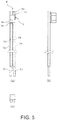
- Fig. 5(a) ⁇ Fig. 5(c) are a top view, a side view, and a front view, respectively, illustrating a thermistor module with leads according to the second embodiment of the present invention.
- the predetermined interval in the lead length direction of the metal wire exposed portions 3a, 3b is equal to or slightly larger than the distance between the two terminal electrodes of the thermistor 1.
- the thermistor 1 can be mounted on the joint surfaces of the first and second leads on the same side in such a manner that the longitudinal direction of the thermistor 1 is parallel to the length direction of the first and second leads.
- the thermistor is provided that the longitudinal direction of the thermistor is parallel to the length direction of the first and second leads, so that when the sum of outer diameter of the first and second leads is equal to or smaller than the width of the thermistor, the width in a direction perpendicular to the lead length direction is equal to the width of the thermistor, and is smaller than the width while the thermistor is provided in an inclined manner at a predetermined angle with respect to the first and second leads, therefore, compared with the first embodiment, the miniaturization can be maximized.
- the thermistor can also be a chip resistor, a chip capacitor, a chip inductor, a piezoelectric element and other chip electronic components with electrodes at both ends.
- Fig. 20 illustrates an example of a configuration of an electronic component module with leads according to the present embodiment.
- the electronic component module may further include an insulating resin 50 which packages the electronic component, as well as a front end of the first and second leads on which the electronic component is mounted.
- the insulating resin 50 By using the insulating resin 50 to package, the environmental adaptability of the electronic component module can be improved.
- the third embodiment it is still preferred to use a thermistor module with leads (also referred to as a temperature sensor) as an electronic component module with leads, for the same reason as in the first embodiment.
- the metal wire exposed portions of the first and second leads respectively extend to the outer peripheral side of the corresponding lead, toward non-adjacent outer directions of the first and second leads.
- the metal wire exposed portions of the first and second leads are respectively coated with solder, if the solder can be applied in direct contact with the metal wire exposed portions, respectively, the solder coating may extend beyond the metal wire exposed portions and extend to the outer peripheral side of the corresponding lead toward non-adjacent outer directions of the first and second leads.
- the area of the solder coating i.e. the contact area between solder and the first and second leads
- the area of the solder coating is slightly larger than the area of the corresponding metal wire exposed portion.
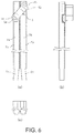
- Fig. 6(a) ⁇ Fig. 6(c) are a top view, a side view, and a front view, respectively, illustrating an example of a thermistor module with leads according to the third embodiment of the present invention. This example corresponds to the case where the length direction of the thermistor and the length direction of the first and second leads have a predetermined angle.
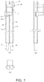
- Fig. 7(a) ⁇ Fig. 7(c) are a top view, a side view, and a front view, respectively, illustrating another example of a thermistor module with leads according to the third embodiment of the present invention. This example corresponds to the case where the length direction of the thermistor is parallel to the length direction of the first and second leads.
- the metal wire exposed portions 3a and 3b of the first and second leads 5a and 5b extend to the outer peripheral side of the corresponding lead toward non-adjacent outer directions of the first and second leads 5a and 5b.
- the metal wire exposed portions of the first and second leads extend to the out peripheral side of the corresponding lead toward non-adjacent outer directions of the first and second leads 5a and 5b, so that the solder coating amount applied to the metal wire exposed portions is more, the solder coating area becomes larger, thereby the area of a solder joint portion becomes larger, with a strong jointing strength which can achieve stable and reliable jointing.
- the solder is applied so as to extend toward the outer direction of the first and second leads to the outer peripheral side of the corresponding lead, even if the solder coating amount is large and the area is large, the metal wire exposed portions of the first and second leads still have sufficient intervals in the lead width direction, under the action of the solder surface tension, the solder will naturally shrink at the terminal electrodes at both ends of the thermistor during melting, which can greatly avoid short-circuit failure.
- the solder in direct contact with the metal wire exposed portions, it is not necessary to strictly control the solder coating position and the coating amount, thereby the difficulty of operation can be reduced as well as the costs, and thus the mass production processing can be achieved.
- the thermistor can also be a chip resistor, a chip capacitor, a chip inductor, a piezoelectric element and other chip electronic components with electrodes at both ends.
- Fig. 20 illustrates an example of a configuration of an electronic component module with leads according to the present embodiment.
- the electronic component module may further include an insulating resin 50 which packages the electronic component, as well as a front end of the first and second leads on which the electronic component is mounted.
- the insulating resin 50 By using the insulating resin 50 to package, the environmental adaptability of the electronic component module can be improved.
- the electronic component may be a chip electronic component having an electrode at both ends, such as a chip resistor, a chip capacitor, a chip inductor, a piezoelectric element, and a thermistor, etc.
- the electronic component is a thermistor.
- the electronic component module according to the fourth embodiment differs from the first embodiment in that, in the fourth embodiment, an end surface of the front end of the first lead for mounting one end of the electronic component body and an end surface of the front end of the second lead for mounting one end of the electronic component body are not aligned with each other and are not continuous.
- “not aligned with each other and are not continuous” can be understood as the end surfaces of the first lead and the second lead are in different planes and edges of the both are not adjacent to each other.
- Fig. 9(a) ⁇ Fig. 9(c) are a top view, a side view, and a front view, respectively, illustrating an example of a electronic component module with leads according to the forth embodiment of the present invention.
- the end surface of the first lead 15a for mounting one end of an electronic component 11 and the end surface of the second lead 15b for mounting one end of the electronic component 11 form a segment difference, that is, the end surface of the first lead 15a for mounting one end of the electronic component 11 is more protruded than the end surface of the second lead 15b for mounting one end of the electronic component 11.
- the first lead 15a extends longer in the length direction with respect to the second lead 15b, so that the edge of the end surface of the first lead 15a and the edge of the end surface of the second lead 15b are not adjacent and cannot come into contact with each other.
- Fig. 10(a) ⁇ Fig. 10(c) are a top view, a side view, and a front view, respectively, illustrating another example of an electronic component module with leads according to the fourth embodiment of the present invention.
- the end surface of the first lead 15a for mounting one end of the electronic component 11 and the end surface of the second lead 15b for mounting one end of the electronic component 11 form a segment difference, specifically, the end surface of the second lead 15b for mounting one end of the electronic component 11 is more protruded than the end surface of the first lead 15a for mounting one end of the electronic component 11.
- the second lead 15b extends longer in the length direction with respect to the first lead 15a, so that the edge of the end surface of the first lead 15a and the edge of the end surface of the second lead 15b are not adjacent and cannot come into contact with each other.
- first lead 15a and the second lead 15b When cutting off the first lead 15a and the second lead 15b covering an insulating layer, incisions with metal burrs or other form of irregular incisions may sometimes be formed. If the front end of the first lead 15a is aligned with the front end of the second lead 15b, it is still easy to make the contact between the conductors, and thus a short-circuit failure occurs.
- the top end surfaces of the first lead 15a and the second lead 15b are formed in the form shown in the Fig. 9(a) ⁇ 9(c) , Fig.10(a) ⁇ 10(c) by cutting or other reasonable means, thereby the risk of the above short-circuit failure can be reduced.
- Fig. 20 illustrates an example of a configuration of an electronic component module with leads according to the present embodiment.
- the electronic component module may further include an insulating resin 50 which packages the electronic component, as well as a front end of the first and second leads on which the electronic component is mounted.
- the insulating resin 50 By using the insulating resin 50 to package, the environmental adaptability of the electronic component module can be improved.
- the electronic component may be a chip electronic component having two electrodes, such as a chip resistor, a chip capacitor, a chip inductor, a piezoelectric element, and a thermistor, etc.
- the electronic component is a thermistor.
- the electronic component module according to the fifth embodiment differs from the first embodiment in that, in the fifth embodiment, the electronic component is rectangular parallelepiped, a gap or a space having a V-shaped cross-sectional shape is formed between the first lead and the second lead, and a long side of the electronic component falls into and is accommodated in the gap or the space having a V-shaped cross-sectional shape.
- Fig. 11(a) ⁇ Fig. 11(c) are a top view, a side view, and a front view, respectively, illustrating an example of an electronic component module with leads according to the fifth embodiment of the present invention. As shown in Fig. 11(a) ⁇ Fig.
- a first lead 15a and a second lead 15b are cylinders, and the first lead 15a and the second lead 15b are brought into close contact with each other to form a V-shaped groove 9a.
- V-shaped it should be understood by those skilled in the art that, it does not refer to an absolute V-shape, it should include a shape similar to the V-shape, for example, the line has a certain degree of curvature or a range of deformation.
- the electronic component 11 is rectangular parallelepiped, when the electronic component 11 is mounted on the first lead 15a and the second lead 15b, a long side 11a of the electronic component 11 falls into the groove 9a.
- the V-shaped groove, or space can also be replaced by a groove, or space of U-shape, or having a concave section.
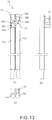
- Fig. 12(a) ⁇ Fig. 12(c) are a top view, a side view, and a front view, respectively, illustrating another example of an electronic component module with leads according to the fifth embodiment of the present invention.
- a gap 9a is left between the first lead 15a and the second lead 15b.
- the electronic component 11 is rectangular parallelepiped, when the electronic component 11 is mounted on the first lead 15a and the second lead 15b, a long side 11a of the electronic component 11 falls into the gap 9a.
- the electronic component can be stably mounted on the first lead 15a and the second lead 15b.
- the structure may have better stability, for example, the longer side 11a of the electronic component is longer, or the diameter of the lead is larger.
- Fig. 20 illustrates an example of a configuration of an electronic component module with leads according to the present embodiment.
- the electronic component module may further include an insulating resin 50 which packages the electronic component, as well as a front end of the first and second leads on which the electronic component is mounted.
- the insulating resin 50 By using the insulating resin 50 to package, the environmental adaptability of the electronic component module can be improved.
- the electronic component may be a chip electronic component having an electrode at both ends, such as a chip resistor, a chip capacitor, a chip inductor, a piezoelectric element, and a thermistor, etc.
- the electronic component is a thermistor.
- the electronic component module with leads according to the sixth embodiment differs from the first embodiment in that, an insulating material is coated between metal wire exposed portions. Since two electrodes of the electronic component are mounted and welded to metal wire exposed portions, there is still a slight risk of short-circuit after welding, although there are insulating members used to isolate the electrical conduction between metal wire exposed portions, for example, the solder of the two electrodes of the electronic component may extend and contact with each other, therefore, it is possible to coat insulating material between metal wire exposed portions to reduce the risk of the short circuit.
- the insulating material may further have an adhesive property, or may be welded, for example, as a connecting method, an epoxy resin in a molten state may be used at the metal wire exposed portions, especially at adjacent area of the first lead, the second lead, and the electronic component, and thus the above three may be welded and fixed to each other, in this way, not only the risk of the above-mentioned short-circuit can be reduced, but also the structure of the electronic component module with leads of the present embodiment can be more stable and less susceptible to external shock, at the same time, it is possible to prevent the electronic component from falling off from the first lead and the second lead while manufacturing.
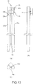
- Fig. 13(a) ⁇ Fig. 13(c) are a top view, a side view, and a front view, respectively, illustrating an example of an electronic component module with leads according to the sixth embodiment of the present invention.
- an insulating material 19 having an adhesive property such as an epoxy resin, is coated.
- the insulating material 19 is coated between metal wire exposed portions 13a and 13b and is located at adjacent area of the first lead 15a and the second lead 15b.
- the insulating material 19 is located between the metal wire exposed portions 13a, 13b and is therefore also located between the electrodes 12a, 12b of electronic component 11 and between solder 14a, 14b. As a result, the risk of short-circuit between the solder 14a, 14b and between the electrodes 12a, 12b is reduced. At the same time, taking advantage of adhesive property of the insulating material 19, the first lead 15a, the second lead 15b, and the electronic component 11 are fixed to each other by the adhesion.
- the structure of electronic component module 18 with leads can be more stable and less susceptible to external shock, meanwhile, it is possible to prevent the electronic component 11 from being affected by vibration or the like, which causing the mount position to be shifted or falling off from the first lead 12a and the second lead 12b.
- the insulating material 19 may also extend to the side walls (not shown) of the electronic component 11 between the two terminal electrodes 12a, 12b.That is, after electronic component 11 is mounted and welded to metal wire exposed portions 13a and 13b, the insulating material 19 is not only located at adjacent area of the first lead 15a, the second lead 15b and the electronic element 11, but also extends and is adhered to the side wall of the electronic component 11 located between the two terminal electrodes 12a and 12b through melting, coating, deformation and other means, and the insulating material 19 may cover a part or all of the side wall.
- the electronic component 11 itself is likely to be a semiconductor material, and if the insulating material 19 covers all of the side wall, the influence on the characteristics of the electronic component due to the solder extension on the terminal electrodes 12a, 12b is reduced, on the other hand, such structure can further prevent the solder extension on the terminal electrodes 12a, 12b from causing a short-circuit.
- Fig. 14 illustrates a top view of another example of an electronic component module with leads according to the sixth embodiment of the present invention.
- an insulating material 19 having an adhesive property is also provided between metal wire exposed portions 13a and 13b, the coverage of insulating material 19 is increased so that a part of metal wire exposed portions 13a, 13b is covered by the insulating material 19.As a result, the short-circuit risk is further reduced. Even if the distance between metal wire exposed portions 13a, 13b is very small, it is difficult for the solder to bypass the area covered by the insulating material 19 to cause a short-circuit.
- Fig. 15 illustrates a top view of another example of an electronic component module with leads according to the sixth embodiment of the present invention.
- the coverage of the insulating material 19 can be further increased, thereby more effectively reducing the above-mentioned short-circuit risk.
- the metal wire exposed portions 13a, 13b are completely exposed, not covered by insulating material 19. Since the insulating material 19 does not cover the metal wire exposed portions 13a, 13b, the metal wire exposed portions 13a, 13b can be brought into more sufficient contact with the electrodes of electronic component 11. Meanwhile the manufacturing process can also be more simplified (please refer to the method section below).
- the sixth embodiment also relates to a method of manufacturing the above-described electronic component module with leads.
- one example of manufacturing steps of above-described electronic component module with leads include the following steps.
- Step a as shown in Fig. 16(a) , prepare two metal wires covered with an insulating member to form parallel leads 5a, 5b arranged side by side.
- Step b as shown in Fig. 16(b) , on the joint surfaces of the first and second leads 15a, 15b on the same side and used for jointing with the terminal electrodes 12a, 12b of the thermistor 1, metal wires are exposed from the first and second leads 15a, 15b by stripping a certain area of the insulating member, respectively, therefore metal wire exposed portions 13a, 13b are formed.
- the metal wire exposed portions 13a, 13b do not overlap each other in lead length direction and are spaced apart with a predetermined interval L.
- the insulating material 19 is coated between metal wire exposed portions 13a, 13b, the coverage of the insulating material 19 may include a part of the metal wire exposed portions 13a, 13b (as shown in Fig.14 ), or may be formed without covering the metal wire exposed portions 13a, 13b as shown in Fig. 13(a) .
- Insulating material 19 may be made of an epoxy resin or the like.
- Step d as shown in Fig. 16(d) , the metal wire exposed portions 13a and 13b are respectively coated with solder 14a and 14b.
- the solder 14a and 14b are composed of Sn-Ag-Cu, for example.
- Step e as shown in Fig. 16(e) , two terminal electrodes 12a, 12b of electronic component 11 are respectively in contact with solder 14a, 14b.
- Step f as shown in Fig. 16(f) , the solder is melted at a specific temperature for a specific period of time, so that the terminal electrodes 12a, 12b of electronic component 11 are jointed and fixed to the metal wire exposed portions 13a, 13b by soldering.
- the electronic component 11 moves to a stable position naturally and fixed under an action of a surface tension of the solder.
- the electronic component 11 is finally mounted on the first and second leads 15a, 15b in an inclined manner so as to have a predetermined angle with respect to the length direction of the first and second leads 15a, 15b.
- Step g as shown in Fig. 16(g) , the insulating resin 50 used for packaging is applied to cover the first and second leads 15a and 15b, the solder and the electronic component 11, and then solidification treatment is performed at a specific temperature for a specific time, thereby a electronic component module 18 with leads is manufactured.
- an area of the metal wire exposed portions 13a, 13b of the first and second leads 15a, 15b is equal to or greater than the jointing area of the terminal electrodes 12a, 12b of the electronic component 11 and the corresponding metal wire exposed portions (the area of a joint surface where the terminal electrode is connected to the metal wire exposed portion by soldering), preferably that the area of the metal wire exposed portions 13a, 13b of the first and second leads 15a, 15b is equal to or slightly greater than the area of an end surface portion of the terminal electrodes 12a, 12b of the electronic component 11 used for jointing to the corresponding metal wire exposed portions.
- the adjacent edges of the metal wire exposed portions 13a, 13b in the lead length direction are respectively overlapped with the attaching surfaces of the terminal electrodes 12a, 12b of the electronic component 11.
- the electronic component 11 can be installed after the first and second leads 15a, 15b are cut to a proper length, and the lead cutting can also be performed after the installation of the electronic component 11 is finished by soldering.
- the coated insulating material 19 may have an adhesive or a welding effect to fix electronic component 11 onto the first and second leads 15a, 15b, thereby it is possible to ensure that the electronic component 11 does not shift or fall off due to the movement or vibration of the first and second leads 15a and 15b before the welding is completed.
- the solder since the solder is in a molten state during welding, it is possible to prevent the electronic component 11 from being shifted due to contact, thermal expansion, shrinkage, and the like.
- Fig. 17(a) ⁇ Fig. 17(b) illustrate step b', step c' of another example in manufacturing steps of an electronic component module with leads according to the sixth embodiment.
- the example is different from the example shown in Figs. 16 (a) -16 (g) in that, step b and step c are changed to step b' , step c'.
- the steps b' and c' will be described in detail below. And since the other steps of the two examples are the same, they are not described here.
- Step b' as shown in Fig. 17(a) , in the regions of the first and second leads 15a and 15b for mounting the electronic component 11, the insulating material 19 is coated.
- Step c' as shown in Fig. 17(b) , on the joint surfaces of the first and second leads 15a, 15b on the same side and used for jointing with the terminal electrodes 12a, 12b of the electronic component 11, metal wires are exposed from the first and second leads 15a, 15b by stripping a certain area of the insulating member and the insulating material 19 adhered to, respectively, therefore metal wire exposed portions 13a, 13b are formed.
- the metal wire exposed portions 13a, 13b do not overlap each other in the lead length direction and are spaced apart with a predetermined interval L.
- the insulating material 19 is not adhered, but the partial edges of metal wire exposed portions 13a and 13b are surrounded by the insulating material 19.
- the insulating material 19 can be coated onto the first and second leads 15a and 15b at a relatively low accuracy (That is, there is no need for a very precise positioning of the coating for insulating material), so that the production efficiency can be improved.
- Fig. 18(a) ⁇ Fig. 18(c) are a top view, a side view, and a front view, respectively, illustrating another example of an electronic component module with leads according to the sixth embodiment.
- the end surface of the first lead 15a for mounting one end of the electronic component 11 and the end surface of the second lead 15b for mounting one end of the electronic component 11 form a segment difference, that is, the end surface of the first lead 15a for mounting one end of the electronic component 11 is more protruded than the end surface of the second lead 15b for mounting one end of the electronic component 11.
- the first lead 15a extends longer in the length direction with respect to the second lead 15b, so that the edge of the end surface of the first lead 15a and the edge of the end surface of the second lead 15b are not adjacent and cannot come into contact with each other.
- an insulating material 19 having an adhesive property such as an epoxy resin, is coated. Specifically, the insulating material 19 is coated between metal wire exposed portions 13a and 13b and is located at adjacent area of the first lead 15a and the second lead 15b.
- Fig. 20 illustrates an example of a configuration of an electronic component module with leads according to the present embodiment.
- the electronic component module may further include an insulating resin 50 which packages the electronic components, as well as a front end of the first and second leads on which the electronic component is mounted.
- the insulating resin 50 By using the insulating resin 50 to package, the environmental adaptability of the electronic component module can be improved.
- the electronic component may be a chip electronic component having an electrode at both ends, such as a chip resistor, a chip capacitor, a chip inductor, a piezoelectric element, and a thermistor, etc.
- a plurality of electronic components are mounted on the first and second leads at a predetermined interval so that the electronic components of electronic component module with leads are connected in parallel for various different applications.
- a thermistor when used as an electronic component, set the most likely hot spot of the battery cell of the mobile phone as a measurement point, and arrange the temperature sensing part of the thermistor, so that it is possible to accurately perform the battery charging and discharging control.
- Fig. 18 illustrates a configuration of an electronic component module with leads according to the seventh embodiment of the present invention when applied to a fuel battery temperature detection.
- battery case 35 is provided with three battery cells 32a, 32b, and 32c inside, and a control board 37 is disposed at the end of the battery case 35.
- the measurement point Since the lead is mounted on the control board 37, the measurement point must be separated from the control board 37 when it is desired to measure the temperature of the battery cell 32b.
- the temperature sensing part of the thermistor can be also arranged at the heat generating portion of a FET (Field Effect Transistor) used for power supply, so that it can be quickly and accurately controlled when the FET generates abnormal heat.
- FET Field Effect Transistor
- a plurality of FETs and a large battery are mounted on an electronic device such as a personal computer, by using a plurality of thermistors connected as shown in Fig. 19 , the temperature measurement can be performed efficiently.
- a thermistor as an electronic component for temperature measurement
- a plurality of other electronic components which can be used as a sensing device and other devices can be connected in parallel to form an electronic component module with leads of the seventh embodiment, to obtain a corresponding function.
- the electronic component module of the present embodiment may further include an insulating resin which packages electronic components, as well as the part of the first and second leads on which electronic components are mounted.
- the insulating resin not shown
- the electronic component is preferably a thermistor, and a lead can be welded and fixed to a control board such as a printed circuit board, the thermistor mounted on the lead can be extended with the lead and placed in a target location where temperature sensing is required or heat changes may occur.
- a control board such as a printed circuit board
- the thermistor mounted on the lead can be extended with the lead and placed in a target location where temperature sensing is required or heat changes may occur.
- the present invention is not limited to the above-described embodiments, and various modifications may be made within the scope of the claims, and the embodiments obtained by appropriately combining the technical means disclosed in the different embodiments are also included in the technical scope of the present invention.
- a non-laminated thermistor without internal electrode may be used, or an electronic component other than a thermistor may be used.
Landscapes
- Engineering & Computer Science (AREA)
- Microelectronics & Electronic Packaging (AREA)
- Power Engineering (AREA)
- Physics & Mathematics (AREA)
- Manufacturing & Machinery (AREA)
- Electromagnetism (AREA)
- Nonlinear Science (AREA)
- General Physics & Mathematics (AREA)
- Thermistors And Varistors (AREA)
Abstract
Description
- The present invention relates to an electronic component module with leads and a method for manufacturing the same.
- In the prior art, in an electronic component module with leads, for example, a thermistor module as a temperature sensor, a thermistor having terminal electrodes formed at both ends thereof is mounted on two parallel leads, a coated insulator of the same front end of the two leads is peeled off to expose metal wires, the exposed metal wires are connected to the terminal electrodes of the thermistor by soldering, respectively.
- As an example, for example,
Patent Document 1 proposes a thermistor module with leads which has the following structure. As shown inFig.8 , a first andsecond leads metal wires members second leads inner wires terminal electrodes thermistor 41 are electrically connected to the corresponding exposedmetal wires solder - Patent Document 1: China Patent Publication No.
101583858 - In
Patent Document 1, the two leads can be arranged in parallel without gaps, and a short-circuit failure is not easily generated. However, since the metal wires are connected to the thermistor while being cut into an oblique shape, the area of a solder joint portion is small and the jointing strength is low. Furthermore, when the diameter of the leads is relatively small, the area of the solder joint portion is reduced accordingly, and the jointing strength is further lowered, especially in thermal shock, circuit breakage is likely to occur due to the break of the solder joint portion. Besides, when cutting the front ends of the two leads at a specific angle, the smaller the lead diameter, the higher the accuracy of the cutting process requested, so that it is difficult to realize the installation of the thermistor on leads with smaller diameter. - The present invention has been made in view of the above circumstances, and an object of the present invention is to provide an electronic component module with leads which is capable of preventing short-circuit failure while ensuring a jointing strength and a method of manufacturing the same.
- In order to achieve the above object, the electronic component module with leads according to the present invention includes an electronic component having terminal electrodes formed at both ends of the electronic component body, and a first and second leads formed by covering metal wires with insulating members and arranged side-by-side while the first and second leads are electrically connected to the terminal electrodes, characterized in that metal wire exposed portions where the metal wires are exposed respectively from the first and second leads are provided on joint surfaces of the first and second leads on the same side which is used for jointing to the terminal electrodes, the metal wire exposed portion of the first lead and the metal wire exposed portion of the second lead are spaced apart from each other by a predetermined interval in the lead length direction, the terminal electrodes are electrically connected to the metal wire exposed portions of the first and second leads, respectively, by soldering.
- In the electronic component module with leads according to the present invention, it is preferable that the electronic component is provided with a predetermined angle between the longitudinal direction and the lead length direction.
- In the electronic component module with leads according to the present invention, it is preferable that the electronic component is provided that the longitudinal direction is parallel to the lead length direction.
- In the electronic component module with leads according to the present invention, it is preferable that the area of the metal wire exposed portion of the first and second leads is equal to or greater than the jointing area of the terminal electrodes and the corresponding metal wire exposed portions, respectively.
- In the electronic component module with leads according to the present invention, it is preferable that the metal wire exposed portions of the first and second leads respectively extend to the outer peripheral side of the corresponding lead, toward non-adjacent outer directions of the first and second leads.
- In the electronic component module with leads according to the present invention, it is preferable that an end surface of the first lead for mounting one end of the electronic component and an end surface of the second lead for mounting one end of the electronic component are not aligned with each other and are not continuous.
- In the electronic component module with leads according to the present invention, it is preferable that the end surface of the first lead for mounting one end of the electronic component is protruded as compared with the end surface of the second lead for mounting one end of the electronic component.
- In the electronic component module with leads according to the present invention, it is preferable that, an insulating material is provided between the metal wire exposed portions.
- In the electronic component module with leads according to the present invention, it is preferable that, the insulating material covers a part of the metal wire exposed portion.
- In the electronic component module with leads according to the present invention, it is preferable that, the insulating material doesn't cover the metal wire exposed portion.
- In the electronic component module with leads according to the present invention, it is preferable that, the insulating material extends to a side wall of the electronic component between the two terminal electrodes.
- In the electronic component module with leads according to the present invention, it is preferable that, the first and second leads, the electronic component are fixed to each other by the insulating material.
- In the electronic component module with leads according to the present invention, it is preferable that, a plurality of the electronic components are mounted on the first lead and the second lead at a predetermined interval.
- In the electronic component module with leads according to the present invention, it is preferable that, the electronic component is a thermistor.
- In the electronic component module with leads according to the present invention, it is preferable that, the thermistor is a surface-mount type thermistor.
- In the electronic component module with leads according to the present invention, it is preferable that, the surface- mount type thermistor includes an internal electrode.
- A method of manufacturing an electronic component module with leads according to the present invention is a method for mounting an electronic component having terminal electrodes formed at both ends of the electronic component body onto a first and second leads which formed by covering metal wires with insulating members and arranged side-by-side, characterized in that it comprises: a step of forming metal wire exposed portions where the metal wires are exposed respectively from the first and second leads on joint surfaces of the first and second leads on the same side which is used for jointing to the terminal electrodes, and separating the metal wire exposed portion of the first lead from the metal wire exposed portion of the second lead by a predetermined interval in a lead length direction; a step of applying solder to the metal wire exposed portion of the first and second leads, respectively; and a step of bringing the terminal electrodes into contact with the solder of the metal wire exposed portions of the first and second leads, respectively, and heating the solder to melt so that the terminal electrodes are respectively jointed to the metal wire exposed portions of the first and second leads.
- In the method of manufacturing an electronic component module with leads according to the present invention, it is preferable that, the electronic component is provided with a predetermined angle between the longitudinal direction and the lead length direction.
- In the method of manufacturing an electronic component module with leads according to the present invention, it is preferable that, the electronic component is provided that the longitudinal direction is parallel to the lead length direction.
- In the method of manufacturing an electronic component module with leads according to the present invention, it is preferable that, the method of manufacturing an electronic component module with leads further includes a step of applying an insulating material between the metal wire exposed portions of the first and second leads.
- In the method of manufacturing an electronic component module with leads according to the present invention, it is preferable that, when the insulating material is applied between the metal wire exposed portions, the insulating material also covers a part of the metal wire exposed portions.
- The present invention also relates to a method of manufacturing an electronic component module with leads, for mounting an electronic component having terminal electrodes formed at both ends of the electronic component body onto a first and second leads which formed by covering metal wires with insulating members and arranged side-by-side, characterized in that it comprises: a step of applying an insulating material to joint surfaces of the first and second leads on the same side which are used for jointing to the terminal electrodes, as well as its periphery thereof, removing the insulating members as well as the insulating material for forming metal wire exposed portions where the metal wires are exposed respectively from the first and second leads, and separating the metal wire exposed portion of the first lead and the metal wire exposed portion of the second lead from each other by a predetermined interval in the lead length direction; a step of applying solder to the metal wire exposed portion of the first and second leads, respectively; and a step of bringing the terminal electrodes into contact with the solder of the metal wire exposed portions of the first and second leads, respectively, and heating the solder to melt so that the terminal electrodes are respectively jointed to the metal wire exposed portions of the first and second leads.
- According to the present invention, since the metal wire exposed portions are formed on the joint surfaces of the first and second leads on the same side, the solder can be applied to the metal wire exposed portions to ensure conduction, even if the diameter of the first and second leads are small, it is possible to control the solder coating amount and the jointing area by controlling the area of the metal wire exposed portions, to ensure a sufficient solder joint surface, thereby obtain a strong jointing strength as well as improved reliability and environmental resistance. Meanwhile, since the metal wire exposed portions of the first and second leads are spaced apart from each other by a predetermined interval in the lead length direction, bridging or migration of the solder is less likely to occur even if more solder is applied, so that the short circuit between the terminal electrodes of the electronic components is avoided, and the short-circuit failure is less likely to occur.
- According to the present invention, since the electronic components are mounted on the joint surfaces of the first and second leads on the same side, it is not necessary to perform end surface machining for the front ends of the first and second leads, and is possible to eliminate the restriction of the cutting process when the diameter of the first and second leads is small, thereby obtain a smaller electronic component module with leads with low cost, sufficient stability, and stable reliability in terms of heat and mechanical. Furthermore, when the thermistor is mounted on the joint surfaces of the first and second leads on the same side, the electronic components do not fall of before the solder melted, therefore, the position of the electronic components does not need to be fixed before soldering, which is easy to process.
-
-
Fig. 1(a) is a solid diagram illustrating a thermistor used in a thermistor module with leads according to a first embodiment of the present invention,Fig. 1(b) is a cross-sectional view taken along the line A-A' inFig. 1(a) . -
Fig. 2(a) ∼ Fig. 2(c) are a top view, a side view, and a front view, respectively, illustrating a thermistor module with leads according to the first embodiment of the present invention. -
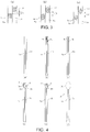
Fig. 3(a) ∼ Fig. 3(c) illustrate different shapes of metal wire exposed portions in a thermistor module with leads in a top view according to the first embodiment of the present invention. -
Fig. 4(a) ∼ Fig. 4(f) illustrate manufacturing steps of a thermistor module with leads according to the first embodiment of the present invention. -
Fig. 5(a) ∼ Fig. 5(c) are a top view, a side view, and a front view, respectively, illustrating a thermistor module with leads according to a second embodiment of the present invention. -
Fig. 6(a) ∼ Fig. 6(c) are a top view, a side view, and a front view, respectively, illustrating an example of a thermistor module with leads according to a third embodiment of the present invention. -
Fig. 7(a) ∼ Fig. 7(c) are a top view, a side view, and a front view, respectively, illustrating another example of a thermistor module with leads according to the third embodiment of the present invention. -
Fig. 8 illustrates a top view of a thermistor module with leads disclosed inPatent Document 1. -
Fig. 9(a) ∼ Fig. 9(c) are a top view, a side view, and a front view, respectively, illustrating an example of a thermistor module with leads according to a fourth embodiment of the present invention. -
Fig. 10(a) ∼ Fig. 10(c) are a top view, a side view, and a front view, respectively, illustrating another example of a thermistor module with leads according to the fourth embodiment of the present invention. -
Fig. 11(a) ∼ Fig. 11(c) are a top view, a side view, and a front view, respectively, illustrating an example of a thermistor module with leads according to a fifth embodiment of the present invention. -
Fig. 12(a) ∼ Fig. 12(c) are a top view, a side view, and a front view, respectively, illustrating another example of a thermistor module with leads according to the fifth embodiment of the present invention. -
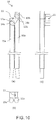
Fig. 13(a) ∼ Fig. 13(c) are a top view, a side view, and a front view, respectively, illustrating an example of a thermistor module with leads according to a sixth embodiment of the present invention. -
Fig. 14 illustrates a top view of another example of a thermistor module with leads according to the sixth embodiment of the present invention. -
Fig. 15 illustrates a top view of another example of a thermistor module with leads according to the sixth embodiment of the present invention. -
Fig. 16(a) ∼ Fig. 16(g) illustrate an example of a method of manufacturing a thermistor module with leads according to the sixth embodiment of the present invention. -
Fig. 17(a) ∼ Fig. 17(b) illustrate step b', step c' of another example of a method of manufacturing a thermistor module with leads according to the sixth embodiment of the present invention. -
Fig. 18(a) ∼ Fig. 18(c) are a top view, a side view, and a front view, respectively, illustrating another example of a thermistor module with leads according to the sixth embodiment of the present invention. -
Fig. 19 illustrates a configuration of an electronic component module with leads according to a seventh embodiment of the present invention when applied to a fuel battery temperature detection. -
Fig. 20 illustrates an example of a configuration of an electronic component module with leads according to the first to sixth embodiment of the present invention. - Hereinafter, preferred embodiments of the present invention will be described in detail with reference to the accompanying drawings. Here, the same reference numbers are assigned to the same structures, and the repetitive description is omitted.
- The present embodiment provides a thermistor module with leads (also referred to as a temperature sensor) as an electronic component module with leads.
- First, a thermistor module with leads according to the first embodiment of the present invention will be described.
Fig. 1(a) is a solid diagram illustrating athermistor 1 used in a thermistor module with leads concerning the present embodiment,Fig. 1(b) is a cross-sectional view taken along the line A-A' inFig. 1(a) . - As shown in
Fig. 1(a) , thethermistor 1 is preferably a surface-mount type thermistor having an internal electrode. Thethermistor 1 has a thermistor body mainly composed of ceramic material, and twoterminal electrodes terminal electrodes Fig. 1(b) , theinternal electrode 110 is formed inside the thermistor body. - Among them, the electronic component is preferably a thermistor, and leads can be welded and fixed to a control board such as a printed circuit board, the thermistor mounted on the lead can be extended with the lead and placed in a target location where temperature sensing is required or heat changes may occur.
- Furthermore, by using a surface-mount type thermistor, the distance between the terminal electrodes can be larger, and it is difficult to generate a migration, so that the short circuit between the terminal electrodes can be greatly prevented. In addition, since the thermistor has an internal electrode, it is difficult to produce the electrode peeling, and the influence on the resistance value is small even when the electrode is peeled off.
-
Fig. 2(a) ∼ Fig. 2(c) are a top view, a side view, and a front view, respectively, illustrating athermistor module 8 with leads concerning the first embodiment of the present invention. - As shown in
Fig. 2 , the first andsecond leads first lead 5a and thesecond lead 5b may be jointed as a whole in the lead length direction to form a set of parallel leads. Further, the first lead and the second lead may not be jointed as a whole. - In the first and
second leads member 7a, and the metal wire (core) 6b is covered with the insulating member 7b.Themetal wires members - As shown in
Fig. 2(a) , in thefirst lead 5a, on a joint surface thereof for jointing to oneterminal electrode 2a of thethermistor 1, a metal wire exposedportion 3a where themetal wire 6a is exposed from thefirst lead 5a by stripping a part of the insulatingmember 7a is provided. Similarly, in thesecond lead 5b, on a joint surface thereof located on the same side with the joint surface of thefirst lead 5a, for jointing to the otherterminal electrode 2b of thethermistor 1, a metal wire exposedportion 3b where themetal wire 6b is exposed from thesecond lead 5b by stripping a part of the insulatingmember 7b is provided. - The metal wire exposed
portion 3a of thefirst lead 5a and the metal wire exposedportion 3b of thesecond lead 5b are spaced apart by a predetermined interval L (seeFig. 3 ) in the lead length direction. The predetermined interval L is a distance between the adjacent edges of the metal wire exposedportions portions second leads terminal electrodes thermistor 1. - In a top view, the metal wire exposed
portions second leads Figs. 3 (a) to 3 (c) , respectively, rectangular, oval, and irregular shape. - In addition, the metal wire exposed
portion 3a is coated with asolder 4a, and the metal wire exposedportion 3b is coated with a solder 4b.Thesolder solder portions second leads thermistor 1 is electrically connected to the metal wire exposedportion 3a of thefirst lead 5a, and the other terminal electrode of thethermistor 1 is electrically connected to the metal wire exposedportion 3b of thesecond lead 5b. - Specifically, when the
solder portions thermistor 1 can naturally move to a stable position and be fixed under an action of a surface tension of the solder. Therefore, thethermistor 1 is finally mounted on the first andsecond leads terminal electrodes portions - Moreover,
Fig. 20 illustrates an example of a configuration of an electronic component module with leads according to the present embodiment. As shown inFig. 20 , the electronic component module may further include an insulatingresin 50 which packages a front end of the first and second leads on which the electronic component is mounted. By using the insulatingresin 50 to package, the environmental adaptability of the electronic component module can be improved. - Hereinafter, the manufacturing steps of the thermistor module with leads will be described in detail with reference to
Figs. 4(a) to 4(f) . - First of all, as shown in
Fig. 4(a) , prepare two metal wires covered with insulating members to formparallel leads - Next, as shown in
Fig. 4(b) , on the joint surfaces of the first andsecond leads terminal electrodes thermistor 1, metal wires are exposed from the first andsecond leads portions portions terminal electrodes thermistor 1. - Next, as shown in
Fig. 4(c) , the metal wire exposedportions solder 4a and 4b.Thesolder - Then, as shown in
Fig. 4(d) , twoterminal electrodes thermistor 1 are respectively in contact withsolder - Next, as shown in
Fig. 4(e) , the solder is melted in a heating process at a specific temperature for a specific period of time, so that theterminal electrodes thermistor 1 are jointed and fixed to the metal wire exposedportions thermistor 1 moves to a stable position naturally and is fixed under an action of a surface tension of the solder. According to the first embodiment, thethermistor 1 is finally mounted on the first andsecond leads second leads - Then, as shown in
Fig. 4(f) , the insulatingresin 50 used for packaging is applied to cover the first andsecond leads thermistor 1, and then solidification treatment is performed at a specific temperature for a specific period of time, thereby athermistor module 8 with leads is manufactured. - In addition, an area of the metal wire exposed
portions second leads terminal electrodes thermistor 1 and the corresponding metal wire exposed portions (the area of a joint surface where the terminal electrode is connected to the metal wire exposed portion by soldering), preferably that the area of the metal wire exposedportions second leads terminal electrodes thermistor 1 used for jointing to the corresponding metal wire exposed portions. In addition, the adjacent edges of the metal wire exposedportions terminal electrodes thermistor 1. - In addition, the
thermistor 1 can be installed after the first andsecond leads thermistor 1 is finished by soldering. - As mentioned above, according to the first embodiment, since the metal wire exposed portions are formed on the joining surfaces of the first and second leads on the same side, the solder can be applied to the metal wire exposed portions to ensure conduction, even if the diameter of the first and second leads are small, it is possible to control the solder coating amount and the jointing area by controlling the area of the metal wire exposed portions, to ensure a sufficient solder joint surface, thereby obtain a strong jointing strength as well as improved reliability and environmental resistance. Meanwhile, since the metal wire exposed portions of the first and second leads are spaced apart from each other by a predetermined interval in the lead length direction, bridging or migration of the solder is less likely to occur even if more solder is applied, so that the short circuit between the terminal electrodes of the thermistor is avoided, and the short-circuit failure is less likely to occur. In addition, a short-circuit failure is not likely to occur even if the thermistor is not covered with the insulator as in
Patent Document 1. - According to the first embodiment, since the thermistor is mounted on the joint surfaces of the first and second leads on the same side, it is not necessary to perform end surface machining for the front ends of the first and second leads, and is possible to eliminate the restriction of the cutting process when the diameter of the first and second leads is small, and the stress for the thermistor is small in the lead length direction, thereby obtain a smaller thermistor module with leads with low cost, sufficient stability, and stable reliability in terms of heat and mechanical. Furthermore, when the thermistor is mounted on the joint surfaces of the first and second leads on the same side, the thermistor does not fall off before the solder melted, therefore, the position of the thermistor does not need to be fixed before soldering, which is easy to process.
- In addition, according to the first embodiment, the terminal electrodes of the thermistor are electrically connected to the metal wire exposed portions of the first and second leads by soldering, when melting the solder during processing, the thermistor can naturally move to a stable position and be fixed under an action of a surface tension of the solder, as a result, placing position of the thermistor does not need to be strictly controlled before soldering, as long as the dimensional accuracy of the thermistor itself is controlled, it is possible to ensure that the thermistor stably rests in the proper position, making it easy to process.
- In addition, according to the first embodiment, the area of the metal wire exposed portions is equal to or greater than the jointing area between the terminal electrodes of the thermistor and the metal wire exposed portions, so that sufficient exposed portions of metal wires are ensured, and enough area of the solder joint portion is guaranteed, and the distance between the respective metal wire exposed portions of the first and second leads and the terminal electrodes of the thermistor gets closer, thereby, the solder jointing strength and the environmental resistance are ensured, and particularly the resistance to thermal shock is improved.
- Besides, according to the first embodiment, the thermistor can also be a chip resistor, a chip capacitor, a chip inductor, a piezoelectric element and other chip electronic components with electrodes at both ends.
- Next, an electronic component module with leads according to the second embodiment will be described. In the second embodiment, it is still preferred to use a thermistor module with leads (also referred to as a temperature sensor) as an electronic component module with leads, for the same reason as in the first embodiment. The thermistor module with leads according to the second embodiment differs from the first embodiment in that, in the first embodiment, the thermistor is provided with a predetermined angle between the longitudinal direction and the length direction of the first and second leads, but in the second embodiment, the thermistor is provided that the longitudinal direction is parallel to the length direction of the first and second leads. In the following, only the differences will be described.
-
Fig. 5(a) ∼ Fig. 5(c) are a top view, a side view, and a front view, respectively, illustrating a thermistor module with leads according to the second embodiment of the present invention. - Specifically, in the second embodiment, the predetermined interval in the lead length direction of the metal wire exposed
portions thermistor 1. As a result, thethermistor 1 can be mounted on the joint surfaces of the first and second leads on the same side in such a manner that the longitudinal direction of thethermistor 1 is parallel to the length direction of the first and second leads. - According to the second embodiment, the thermistor is provided that the longitudinal direction of the thermistor is parallel to the length direction of the first and second leads, so that when the sum of outer diameter of the first and second leads is equal to or smaller than the width of the thermistor, the width in a direction perpendicular to the lead length direction is equal to the width of the thermistor, and is smaller than the width while the thermistor is provided in an inclined manner at a predetermined angle with respect to the first and second leads, therefore, compared with the first embodiment, the miniaturization can be maximized.
- Besides, according to the second embodiment, the thermistor can also be a chip resistor, a chip capacitor, a chip inductor, a piezoelectric element and other chip electronic components with electrodes at both ends.
- Moreover,
Fig. 20 illustrates an example of a configuration of an electronic component module with leads according to the present embodiment. As shown inFig. 20 , the electronic component module may further include an insulatingresin 50 which packages the electronic component, as well as a front end of the first and second leads on which the electronic component is mounted. By using the insulatingresin 50 to package, the environmental adaptability of the electronic component module can be improved. - Next, an electronic component module with leads according to the third embodiment will be described. In the third embodiment, it is still preferred to use a thermistor module with leads (also referred to as a temperature sensor) as an electronic component module with leads, for the same reason as in the first embodiment. In the third embodiment, the metal wire exposed portions of the first and second leads respectively extend to the outer peripheral side of the corresponding lead, toward non-adjacent outer directions of the first and second leads.
- In the third embodiment, the metal wire exposed portions of the first and second leads are respectively coated with solder, if the solder can be applied in direct contact with the metal wire exposed portions, respectively, the solder coating may extend beyond the metal wire exposed portions and extend to the outer peripheral side of the corresponding lead toward non-adjacent outer directions of the first and second leads. In the case where it is ensured that the metal wire exposed portions of the first and second leads have a predetermined interval in the lead length direction, the area of the solder coating (i.e. the contact area between solder and the first and second leads) is slightly larger than the area of the corresponding metal wire exposed portion.
-
Fig. 6(a) ∼ Fig. 6(c) are a top view, a side view, and a front view, respectively, illustrating an example of a thermistor module with leads according to the third embodiment of the present invention. This example corresponds to the case where the length direction of the thermistor and the length direction of the first and second leads have a predetermined angle. -
Fig. 7(a) ∼ Fig. 7(c) are a top view, a side view, and a front view, respectively, illustrating another example of a thermistor module with leads according to the third embodiment of the present invention. This example corresponds to the case where the length direction of the thermistor is parallel to the length direction of the first and second leads. - As can be seen from
Fig. 6 andFig. 7 , the metal wire exposedportions second leads second leads - According to the third embodiment, the metal wire exposed portions of the first and second leads extend to the out peripheral side of the corresponding lead toward non-adjacent outer directions of the first and
second leads - In addition, since the solder is applied so as to extend toward the outer direction of the first and second leads to the outer peripheral side of the corresponding lead, even if the solder coating amount is large and the area is large, the metal wire exposed portions of the first and second leads still have sufficient intervals in the lead width direction, under the action of the solder surface tension, the solder will naturally shrink at the terminal electrodes at both ends of the thermistor during melting, which can greatly avoid short-circuit failure. In addition, in the case where the solder is in direct contact with the metal wire exposed portions, it is not necessary to strictly control the solder coating position and the coating amount, thereby the difficulty of operation can be reduced as well as the costs, and thus the mass production processing can be achieved.
- Besides, according to the third embodiment, the thermistor can also be a chip resistor, a chip capacitor, a chip inductor, a piezoelectric element and other chip electronic components with electrodes at both ends.
- Moreover,
Fig. 20 illustrates an example of a configuration of an electronic component module with leads according to the present embodiment. As shown inFig. 20 , the electronic component module may further include an insulatingresin 50 which packages the electronic component, as well as a front end of the first and second leads on which the electronic component is mounted. By using the insulatingresin 50 to package, the environmental adaptability of the electronic component module can be improved. - Next, an electronic component module with leads according to the fourth embodiment will be described. According to the fourth embodiment, the electronic component may be a chip electronic component having an electrode at both ends, such as a chip resistor, a chip capacitor, a chip inductor, a piezoelectric element, and a thermistor, etc. In the fourth embodiment, it is preferable that the electronic component is a thermistor.
- The electronic component module according to the fourth embodiment differs from the first embodiment in that, in the fourth embodiment, an end surface of the front end of the first lead for mounting one end of the electronic component body and an end surface of the front end of the second lead for mounting one end of the electronic component body are not aligned with each other and are not continuous. Here, "not aligned with each other and are not continuous" can be understood as the end surfaces of the first lead and the second lead are in different planes and edges of the both are not adjacent to each other.
- In the following, only the differences will be described.
-
Fig. 9(a) ∼ Fig. 9(c) are a top view, a side view, and a front view, respectively, illustrating an example of a electronic component module with leads according to the forth embodiment of the present invention. As shown inFig. 9(a) ∼ Fig. 9(c) , the end surface of thefirst lead 15a for mounting one end of anelectronic component 11 and the end surface of thesecond lead 15b for mounting one end of theelectronic component 11 form a segment difference, that is, the end surface of thefirst lead 15a for mounting one end of theelectronic component 11 is more protruded than the end surface of thesecond lead 15b for mounting one end of theelectronic component 11. It also can be said that, thefirst lead 15a extends longer in the length direction with respect to thesecond lead 15b, so that the edge of the end surface of thefirst lead 15a and the edge of the end surface of thesecond lead 15b are not adjacent and cannot come into contact with each other. -
Fig. 10(a) ∼ Fig. 10(c) are a top view, a side view, and a front view, respectively, illustrating another example of an electronic component module with leads according to the fourth embodiment of the present invention. As shown inFig. 10(a) ∼ Fig. 10(c) , the end surface of thefirst lead 15a for mounting one end of theelectronic component 11 and the end surface of thesecond lead 15b for mounting one end of theelectronic component 11 form a segment difference, specifically, the end surface of thesecond lead 15b for mounting one end of theelectronic component 11 is more protruded than the end surface of thefirst lead 15a for mounting one end of theelectronic component 11. It also can be said that, thesecond lead 15b extends longer in the length direction with respect to thefirst lead 15a, so that the edge of the end surface of thefirst lead 15a and the edge of the end surface of thesecond lead 15b are not adjacent and cannot come into contact with each other. - When cutting off the
first lead 15a and thesecond lead 15b covering an insulating layer, incisions with metal burrs or other form of irregular incisions may sometimes be formed. If the front end of thefirst lead 15a is aligned with the front end of thesecond lead 15b, it is still easy to make the contact between the conductors, and thus a short-circuit failure occurs. The top end surfaces of thefirst lead 15a and thesecond lead 15b are formed in the form shown in theFig. 9(a)∼9(c) ,Fig.10(a)∼10(c) by cutting or other reasonable means, thereby the risk of the above short-circuit failure can be reduced. - Moreover,
Fig. 20 illustrates an example of a configuration of an electronic component module with leads according to the present embodiment. As shown inFig. 20 , the electronic component module may further include an insulatingresin 50 which packages the electronic component, as well as a front end of the first and second leads on which the electronic component is mounted. By using the insulatingresin 50 to package, the environmental adaptability of the electronic component module can be improved. - Next, an electronic component module with leads according to the fifth embodiment will be described. According to the fifth embodiment, the electronic component may be a chip electronic component having two electrodes, such as a chip resistor, a chip capacitor, a chip inductor, a piezoelectric element, and a thermistor, etc. In the fifth embodiment, it is preferable that the electronic component is a thermistor.
- The electronic component module according to the fifth embodiment differs from the first embodiment in that, in the fifth embodiment, the electronic component is rectangular parallelepiped, a gap or a space having a V-shaped cross-sectional shape is formed between the first lead and the second lead, and a long side of the electronic component falls into and is accommodated in the gap or the space having a V-shaped cross-sectional shape.
- In the following, only the differences will be described.
-
Fig. 11(a) ∼ Fig. 11(c) are a top view, a side view, and a front view, respectively, illustrating an example of an electronic component module with leads according to the fifth embodiment of the present invention. As shown inFig. 11(a) ∼ Fig. 11(c) , afirst lead 15a and asecond lead 15b are cylinders, and thefirst lead 15a and thesecond lead 15b are brought into close contact with each other to form a V-shaped groove 9a.Here, for the "V-shaped", It should be understood by those skilled in the art that, it does not refer to an absolute V-shape, it should include a shape similar to the V-shape, for example, the line has a certain degree of curvature or a range of deformation. Theelectronic component 11 is rectangular parallelepiped, when theelectronic component 11 is mounted on thefirst lead 15a and thesecond lead 15b, along side 11a of theelectronic component 11 falls into the groove 9a.In addition, the V-shaped groove, or space can also be replaced by a groove, or space of U-shape, or having a concave section. -
Fig. 12(a) ∼ Fig. 12(c) are a top view, a side view, and a front view, respectively, illustrating another example of an electronic component module with leads according to the fifth embodiment of the present invention. As shown inFig.12(a) ∼ Fig. 12(c) , agap 9a is left between thefirst lead 15a and the second lead 15b.Theelectronic component 11 is rectangular parallelepiped, when theelectronic component 11 is mounted on thefirst lead 15a and thesecond lead 15b, along side 11a of theelectronic component 11 falls into thegap 9a. - According to the structure shown in
Fig. 11(a)∼11(c) , orFig. 12(a)∼12(c) , the electronic component can be stably mounted on thefirst lead 15a and thesecond lead 15b. In some cases, the structure may have better stability, for example, thelonger side 11a of the electronic component is longer, or the diameter of the lead is larger. - Moreover,
Fig. 20 illustrates an example of a configuration of an electronic component module with leads according to the present embodiment. As shown inFig. 20 , the electronic component module may further include an insulatingresin 50 which packages the electronic component, as well as a front end of the first and second leads on which the electronic component is mounted. By using the insulatingresin 50 to package, the environmental adaptability of the electronic component module can be improved. - Next, an electronic component module with leads according to the sixth embodiment will be described. According to the sixth embodiment, the electronic component may be a chip electronic component having an electrode at both ends, such as a chip resistor, a chip capacitor, a chip inductor, a piezoelectric element, and a thermistor, etc. In the sixth embodiment, it is preferable that the electronic component is a thermistor.
- The electronic component module with leads according to the sixth embodiment differs from the first embodiment in that, an insulating material is coated between metal wire exposed portions. Since two electrodes of the electronic component are mounted and welded to metal wire exposed portions, there is still a slight risk of short-circuit after welding, although there are insulating members used to isolate the electrical conduction between metal wire exposed portions, for example, the solder of the two electrodes of the electronic component may extend and contact with each other, therefore, it is possible to coat insulating material between metal wire exposed portions to reduce the risk of the short circuit. On the other hand, preferably, the insulating material may further have an adhesive property, or may be welded, for example, as a connecting method, an epoxy resin in a molten state may be used at the metal wire exposed portions, especially at adjacent area of the first lead, the second lead, and the electronic component, and thus the above three may be welded and fixed to each other, in this way, not only the risk of the above-mentioned short-circuit can be reduced, but also the structure of the electronic component module with leads of the present embodiment can be more stable and less susceptible to external shock, at the same time, it is possible to prevent the electronic component from falling off from the first lead and the second lead while manufacturing.
- In the following, only the differences will be described.
-
Fig. 13(a) ∼ Fig. 13(c) are a top view, a side view, and a front view, respectively, illustrating an example of an electronic component module with leads according to the sixth embodiment of the present invention. As shown inFig. 13(a) ∼ Fig. 13(c) , between metal wire exposedportions material 19 having an adhesive property, such as an epoxy resin, is coated. Specifically, the insulatingmaterial 19 is coated between metal wire exposedportions first lead 15a and thesecond lead 15b. - According to above structure, the insulating
material 19 is located between the metal wire exposedportions electrodes electronic component 11 and betweensolder solder electrodes material 19, thefirst lead 15a, thesecond lead 15b, and theelectronic component 11 are fixed to each other by the adhesion. The structure ofelectronic component module 18 with leads can be more stable and less susceptible to external shock, meanwhile, it is possible to prevent theelectronic component 11 from being affected by vibration or the like, which causing the mount position to be shifted or falling off from thefirst lead 12a and thesecond lead 12b. - In addition, the insulating
material 19 may also extend to the side walls (not shown) of theelectronic component 11 between the twoterminal electrodes 12a, 12b.That is, afterelectronic component 11 is mounted and welded to metal wire exposedportions material 19 is not only located at adjacent area of thefirst lead 15a, thesecond lead 15b and theelectronic element 11, but also extends and is adhered to the side wall of theelectronic component 11 located between the twoterminal electrodes material 19 may cover a part or all of the side wall. The effect of the above structure is: theelectronic component 11 itself is likely to be a semiconductor material, and if the insulatingmaterial 19 covers all of the side wall, the influence on the characteristics of the electronic component due to the solder extension on theterminal electrodes terminal electrodes -
Fig. 14 illustrates a top view of another example of an electronic component module with leads according to the sixth embodiment of the present invention. As shown inFig. 14 , in this example, an insulatingmaterial 19 having an adhesive property is also provided between metal wire exposedportions material 19 is increased so that a part of metal wire exposedportions portions material 19 to cause a short-circuit. -
Fig. 15 illustrates a top view of another example of an electronic component module with leads according to the sixth embodiment of the present invention. As shown inFig. 15 , in this example, the coverage of the insulatingmaterial 19 can be further increased, thereby more effectively reducing the above-mentioned short-circuit risk. However, the metal wire exposedportions material 19. Since the insulatingmaterial 19 does not cover the metal wire exposedportions portions electronic component 11. Meanwhile the manufacturing process can also be more simplified (please refer to the method section below). - The sixth embodiment also relates to a method of manufacturing the above-described electronic component module with leads.
- As shown in
Fig. 16(a)∼16(g) , one example of manufacturing steps of above-described electronic component module with leads include the following steps. - Step a, as shown in
Fig. 16(a) , prepare two metal wires covered with an insulating member to formparallel leads - Step b, as shown in
Fig. 16(b) , on the joint surfaces of the first andsecond leads terminal electrodes thermistor 1, metal wires are exposed from the first andsecond leads portions portions - Step c, as shown in
Fig. 16(c) , the insulatingmaterial 19 is coated between metal wire exposedportions material 19 may include a part of the metal wire exposedportions Fig.14 ), or may be formed without covering the metal wire exposedportions Fig. 13(a) . Insulatingmaterial 19 may be made of an epoxy resin or the like. - Step d, as shown in
Fig. 16(d) , the metal wire exposedportions solder 14a and 14b.Thesolder - Step e, as shown in
Fig. 16(e) , twoterminal electrodes electronic component 11 are respectively in contact withsolder - Step f, as shown in
Fig. 16(f) , the solder is melted at a specific temperature for a specific period of time, so that theterminal electrodes electronic component 11 are jointed and fixed to the metal wire exposedportions electronic component 11 moves to a stable position naturally and fixed under an action of a surface tension of the solder. In the sixth embodiment, theelectronic component 11 is finally mounted on the first andsecond leads second leads - Step g, as shown in
Fig. 16(g) , the insulatingresin 50 used for packaging is applied to cover the first andsecond leads electronic component 11, and then solidification treatment is performed at a specific temperature for a specific time, thereby aelectronic component module 18 with leads is manufactured. - In addition, an area of the metal wire exposed
portions second leads terminal electrodes electronic component 11 and the corresponding metal wire exposed portions (the area of a joint surface where the terminal electrode is connected to the metal wire exposed portion by soldering), preferably that the area of the metal wire exposedportions second leads terminal electrodes electronic component 11 used for jointing to the corresponding metal wire exposed portions. In addition, the adjacent edges of the metal wire exposedportions terminal electrodes electronic component 11. - In addition, the
electronic component 11 can be installed after the first andsecond leads electronic component 11 is finished by soldering. - Besides, the coated insulating
material 19 may have an adhesive or a welding effect to fixelectronic component 11 onto the first andsecond leads electronic component 11 does not shift or fall off due to the movement or vibration of the first andsecond leads electronic component 11 from being shifted due to contact, thermal expansion, shrinkage, and the like. -
Fig. 17(a) ∼ Fig. 17(b) illustrate step b', step c' of another example in manufacturing steps of an electronic component module with leads according to the sixth embodiment. The example is different from the example shown inFigs. 16 (a) -16 (g) in that, step b and step c are changed to step b' , step c'. The steps b' and c' will be described in detail below. And since the other steps of the two examples are the same, they are not described here. - Step b', as shown in
Fig. 17(a) , in the regions of the first andsecond leads electronic component 11, the insulatingmaterial 19 is coated. - Step c', as shown in
Fig. 17(b) , on the joint surfaces of the first andsecond leads terminal electrodes electronic component 11, metal wires are exposed from the first andsecond leads material 19 adhered to, respectively, therefore metal wire exposedportions portions portions material 19 is not adhered, but the partial edges of metal wire exposedportions material 19. - That is, in the manufacturing steps of the electronic component module with leads as shown in
Fig. 17(a) -17(b) , after the insulatingmaterial 19 is coated on the first andsecond leads portions - As a result, the insulating
material 19 can be coated onto the first andsecond leads -
Fig. 18(a) ∼ Fig. 18(c) are a top view, a side view, and a front view, respectively, illustrating another example of an electronic component module with leads according to the sixth embodiment. In the present example, the end surface of thefirst lead 15a for mounting one end of theelectronic component 11 and the end surface of thesecond lead 15b for mounting one end of theelectronic component 11 form a segment difference, that is, the end surface of thefirst lead 15a for mounting one end of theelectronic component 11 is more protruded than the end surface of thesecond lead 15b for mounting one end of theelectronic component 11. It also can be said that, thefirst lead 15a extends longer in the length direction with respect to thesecond lead 15b, so that the edge of the end surface of thefirst lead 15a and the edge of the end surface of thesecond lead 15b are not adjacent and cannot come into contact with each other. - Between metal wire exposed
portions material 19 having an adhesive property, such as an epoxy resin, is coated. Specifically, the insulatingmaterial 19 is coated between metal wire exposedportions first lead 15a and thesecond lead 15b. - Moreover,
Fig. 20 illustrates an example of a configuration of an electronic component module with leads according to the present embodiment. As shown inFig. 20 , the electronic component module may further include an insulatingresin 50 which packages the electronic components, as well as a front end of the first and second leads on which the electronic component is mounted. By using the insulatingresin 50 to package, the environmental adaptability of the electronic component module can be improved. - Next, an electronic component module with leads according to the seventh embodiment will be described. According to the seventh embodiment, the electronic component may be a chip electronic component having an electrode at both ends, such as a chip resistor, a chip capacitor, a chip inductor, a piezoelectric element, and a thermistor, etc.
- In the seventh embodiment, a plurality of electronic components are mounted on the first and second leads at a predetermined interval so that the electronic components of electronic component module with leads are connected in parallel for various different applications.
- For example, when a thermistor is used as an electronic component, set the most likely hot spot of the battery cell of the mobile phone as a measurement point, and arrange the temperature sensing part of the thermistor, so that it is possible to accurately perform the battery charging and discharging control.
-
Fig. 18 illustrates a configuration of an electronic component module with leads according to the seventh embodiment of the present invention when applied to a fuel battery temperature detection. - In the fuel battery,
battery case 35 is provided with threebattery cells control board 37 is disposed at the end of thebattery case 35. - Since the lead is mounted on the
control board 37, the measurement point must be separated from thecontrol board 37 when it is desired to measure the temperature of thebattery cell 32b. - In this case, by soldering a single thermistor to the first and second leads, it is possible to detect the temperature of the
battery cell 32b. - When it is desired to measure the temperature of all the three
battery cells 32a to 32c, as shown inFig. 20 , on the first andsecond leads thermistors battery cells 32a to 32c. - In addition to temperature detection of fuel battery, the temperature sensing part of the thermistor can be also arranged at the heat generating portion of a FET (Field Effect Transistor) used for power supply, so that it can be quickly and accurately controlled when the FET generates abnormal heat.
- In addition, a plurality of FETs and a large battery are mounted on an electronic device such as a personal computer, by using a plurality of thermistors connected as shown in
Fig. 19 , the temperature measurement can be performed efficiently. - In addition to using a thermistor as an electronic component for temperature measurement, a plurality of other electronic components which can be used as a sensing device and other devices can be connected in parallel to form an electronic component module with leads of the seventh embodiment, to obtain a corresponding function.
- In addition, the electronic component module of the present embodiment may further include an insulating resin which packages electronic components, as well as the part of the first and second leads on which electronic components are mounted. By using the insulating resin (not shown) to package, the environmental adaptability of the electronic component module can be improved.
- In addition, in the present invention, the electronic component is preferably a thermistor, and a lead can be welded and fixed to a control board such as a printed circuit board, the thermistor mounted on the lead can be extended with the lead and placed in a target location where temperature sensing is required or heat changes may occur. The present invention is not limited to the above-described embodiments, and various modifications may be made within the scope of the claims, and the embodiments obtained by appropriately combining the technical means disclosed in the different embodiments are also included in the technical scope of the present invention. For example, in the present invention, a non-laminated thermistor without internal electrode may be used, or an electronic component other than a thermistor may be used.
-
- 1, 31a, 31b, 31c: thermistor
- 2a, 2b, 12a, 12b: terminal electrode
- 3a, 3b, 13a, 13b: metal wire exposed portion
- 4a, 4b, 14a, 14b: solder
- 5a, 15a: first lead
- 5b, 15b: second lead
- 6a, 6b: metal wire
- 7a, 7b: insulating member
- 8, 8': thermistor module with leads
- 19: insulating material
- 50: insulating resin for package
- 110: internal electrode
- 11: electronic component
- 18: electronic component module with leads
- 32a, 32b, 32c: battery cell
- 35: battery case
- 37: control board
Claims (22)
- An electronic component module with leads, comprising:an electronic component having terminal electrodes formed at both ends of said electronic component body; andfirst and second leads formed by covering metal wires with insulating members and arranged side-by-side,said first and second leads are electrically connected to said terminal electrodes, respectively,wherein metal wire exposed portions where the metal wires are exposed respectively from said first and second leads are provided on joint surfaces of said first and second leads on the same side which is used for jointing to said terminal electrodes, and said metal wire exposed portion of said first lead and said metal wire exposed portion of said second lead are spaced apart from each other by a predetermined interval in a lead length direction,said terminal electrodes are electrically connected to said metal wire exposed portions of said first and second leads, respectively, by soldering.
- The electronic component module with leads according to Claim 1, wherein said electronic component is provided with a predetermined angle between a length direction of said electronic component and said lead length direction.
- The electronic component module with leads according to Claim 1, wherein said electronic component is provided that a length direction of said electronic component is parallel to said lead length direction.
- The electronic component module with leads according to anyone of Claim 1-3, wherein an area of said exposed metal wire portions of said first and second leads is equal to or greater than a jointing area of said terminal electrodes and corresponding said exposed metal wire portions, respectively.
- The electronic component module with leads according to anyone of Claim 1-3, wherein said exposed metal wire portions of said first and second leads respectively extends to an outer peripheral side of the corresponding said leads, toward non-adjacent outer directions of said first and second leads.
- The electronic component module with leads according to Claim 1, wherein an end surface of said first lead for mounting one end of said electronic component and an end surface of said second lead for mounting one end of said electronic component are not aligned with each other and are not continuous.
- The electronic component module with leads according to Claim 6, wherein said end surface of said first lead for mounting one end of said electronic component is protruded as compared with said end surface of said second lead for mounting one end of said electronic component.
- The electronic component module with leads according to anyone of Claim 1-3, wherein an insulating material is provided between said metal wire exposed portions.
- The electronic component module with leads according to Claim 8, wherein said insulating material covers a part of said metal wire exposed portions.
- The electronic component module with leads according to Claim 8, wherein said insulating material doesn't cover said metal wire exposed portions.
- The electronic component module with leads according to Claim 8, wherein said insulating material extends to a side wall of said electronic component between two said terminal electrodes.
- The electronic component module with leads according to Claim 8, wherein said first and second leads, said electronic component are fixed to each other by said insulating material.
- The electronic component module with leads according to anyone of Claim 1-3, wherein a plurality of said electronic components are mount on said first lead and said second lead at a predetermined interval.
- The electronic component module with leads according to anyone of Claim 1-3, wherein said electronic component is a thermistor.
- The electronic component module with leads according to Claim 14, wherein said thermistor is a surface-mount type thermistor.
- The electronic component module with leads according to Claim 15, wherein said surface-mount type thermistor includes an internal electrode.
- A method of manufacturing an electronic component module with leads, for mounting an electronic component having terminal electrodes formed at both ends of the electronic component body onto first and second leads which formed by covering metal wires with insulating members and arranged side-by-side, comprising:a step of forming metal wire exposed portions where metal wires are exposed respectively from said first and second leads on joint surfaces of said first and second leads on the same side and for jointing to said terminal electrodes, and spacing said metal wire exposed portion of said first lead and said metal wire exposed portion of said second lead apart from each other by a predetermined interval in a lead length direction;a step of applying solder to said metal wire exposed portions of said first and second leads, respectively; anda step of bringing said terminal electrodes into contact with said solder of said metal wire exposed portions of said first and second leads, respectively, and heating said solder to melt so that said terminal electrodes are respectively jointed to said metal wire exposed portions of said first and second leads.
- The method of manufacturing an electronic component module with leads according to Claim 17, wherein said electronic component is provided with a predetermined angle between a length direction of said electronic component and said lead length direction.
- The method of manufacturing an electronic component module with leads according to Claim 17, wherein said electronic component is provided that a length direction of said electronic component is parallel to said lead length direction.
- The method of manufacturing an electronic component module with leads according to Claim 17,
wherein said method of manufacturing an electronic component module with leads further includes:
a step of applying an insulating material between said metal wire exposed portions of said first and second leads. - The method of manufacturing an electronic component module with leads according to Claim 20, wherein when said insulating material is applied between said metal wire exposed portions, said insulating material also covers a part of said metal wire exposed portions.
- A method of manufacturing an electronic component module with leads, for mounting an electronic component having terminal electrodes formed at both ends of the electronic component body onto a first and second leads which formed by covering metal wires with insulating members and arranged side-by-side, comprising:a step of applying an insulating material to joint surfaces of said first and second leads on the same side and used for jointing to said terminal electrodes, as well as its periphery thereof,removing said insulating members as well as said insulating material for forming metal wire exposed portions where said metal wires are exposed respectively from said first and second leads,and separating said metal wire exposed portion of said first lead and said metal wire exposed portion of said second lead from each other by a predetermined interval in a lead length direction;a step of applying solder to said metal wire exposed portions of said first and second leads, respectively; anda step of bringing said terminal electrodes into contact with said solder of said metal wire exposed portions of said first and second leads, respectively, and heating said solder to melt so that said terminal electrodes are respectively jointed to said metal wire exposed portions of said first and second leads.
Applications Claiming Priority (2)
| Application Number | Priority Date | Filing Date | Title |
|---|---|---|---|
| CN201510621595.7A CN106556468A (en) | 2015-09-25 | 2015-09-25 | Thermistor component with lead and its manufacture method |
| PCT/CN2016/090694 WO2017050000A1 (en) | 2015-09-25 | 2016-07-20 | Electronic component assembly with leads and manufacturing method therefor |
Publications (3)
| Publication Number | Publication Date |
|---|---|
| EP3355040A1 true EP3355040A1 (en) | 2018-08-01 |
| EP3355040A4 EP3355040A4 (en) | 2019-06-19 |
| EP3355040B1 EP3355040B1 (en) | 2021-08-18 |
Family
ID=58385808
Family Applications (1)
| Application Number | Title | Priority Date | Filing Date |
|---|---|---|---|
| EP16847882.4A Active EP3355040B1 (en) | 2015-09-25 | 2016-07-20 | Electronic component assembly with leads and manufacturing method therefor |
Country Status (4)
| Country | Link |
|---|---|
| US (1) | US10176909B2 (en) |
| EP (1) | EP3355040B1 (en) |
| CN (2) | CN106556468A (en) |
| WO (1) | WO2017050000A1 (en) |
Families Citing this family (2)
| Publication number | Priority date | Publication date | Assignee | Title |
|---|---|---|---|---|
| CN108036875B (en) * | 2017-12-20 | 2020-02-07 | 广东爱晟电子科技有限公司 | Quick response temperature sensor and manufacturing method thereof |
| DE102021118569B4 (en) * | 2021-07-19 | 2023-01-26 | Tdk Electronics Ag | NTC sensor and method for manufacturing an NTC sensor |
Family Cites Families (21)
| Publication number | Priority date | Publication date | Assignee | Title |
|---|---|---|---|---|
| NL267879A (en) * | 1960-09-26 | |||
| US3147457A (en) * | 1961-08-02 | 1964-09-01 | Fisher Scientific Co | Temperature probe |
| DE4237224C2 (en) * | 1992-11-04 | 1999-11-04 | Bosch Gmbh Robert | Temperature sensor |
| US5379022A (en) * | 1993-05-03 | 1995-01-03 | Fluke Corporation | Thermistor device with extended operating range |
| JP3305941B2 (en) * | 1996-01-22 | 2002-07-24 | 株式会社村田製作所 | Electronic components |
| JPH11108771A (en) * | 1997-10-06 | 1999-04-23 | Matsushita Electric Ind Co Ltd | Thermistor temperature sensor |
| JP2000138105A (en) * | 1998-10-29 | 2000-05-16 | Murata Mfg Co Ltd | Negative temperature coefficient thermistor device |
| TW463184B (en) * | 1999-04-09 | 2001-11-11 | Murata Manufacturing Co | Temperature sensor, method of producing same and method of mounting same to a circuit board |
| JP3516204B2 (en) * | 1999-11-26 | 2004-04-05 | Tdk株式会社 | How to assemble a sensor for detecting temperature and the sensor |
| US6588931B2 (en) * | 2000-12-07 | 2003-07-08 | Delphi Technologies, Inc. | Temperature sensor with flexible circuit substrate |
| JP2002305101A (en) * | 2001-04-05 | 2002-10-18 | Murata Mfg Co Ltd | Surface-mounted positive temperature characteristic thermistor and manufacturing method therefor |
| CN101583858B (en) * | 2007-06-19 | 2011-11-09 | 株式会社村田制作所 | temperature sensor with leads |
| JP2010073731A (en) * | 2008-09-16 | 2010-04-02 | Murata Mfg Co Ltd | Electronic component with lead wire |
| JP5385218B2 (en) * | 2009-11-16 | 2014-01-08 | 三星エスディアイ株式会社 | Usage of secondary battery |
| CN101882744B (en) * | 2010-05-25 | 2011-11-02 | 张战士 | Connection method of thermistor and wire |
| JP2012182260A (en) * | 2011-02-28 | 2012-09-20 | Mitsubishi Materials Corp | Thermistor element and manufacturing method thereof |
| CN202041316U (en) * | 2011-03-02 | 2011-11-16 | 肇庆爱晟电子科技有限公司 | Transparent packaging thermistor temperature sensor |
| CN202662415U (en) * | 2012-06-19 | 2013-01-09 | 华南理工大学 | Composite type voltage and current protection assembly |
| CN203940931U (en) * | 2014-05-29 | 2014-11-12 | 肇庆爱晟电子科技有限公司 | A kind of novel quick response temperature sensor |
| CN104198078A (en) * | 2014-07-30 | 2014-12-10 | 肇庆爱晟电子科技有限公司 | Rapid response single-side double-electrode glass package NTC (Negative-Temperature-Coefficient) thermistor and manufacturing method thereof |
| CN204479201U (en) * | 2015-03-31 | 2015-07-15 | 常州市惠昌传感器有限公司 | The anti-interference NTC temperature sensor in greenhouse |
-
2015
- 2015-09-25 CN CN201510621595.7A patent/CN106556468A/en not_active Withdrawn
-
2016
- 2016-07-20 EP EP16847882.4A patent/EP3355040B1/en active Active
- 2016-07-20 WO PCT/CN2016/090694 patent/WO2017050000A1/en not_active Ceased
- 2016-07-20 CN CN201680043713.3A patent/CN107949778A/en active Pending
-
2018
- 2018-01-31 US US15/884,846 patent/US10176909B2/en active Active
Also Published As
| Publication number | Publication date |
|---|---|
| EP3355040B1 (en) | 2021-08-18 |
| CN106556468A (en) | 2017-04-05 |
| CN107949778A (en) | 2018-04-20 |
| US20180158581A1 (en) | 2018-06-07 |
| WO2017050000A1 (en) | 2017-03-30 |
| EP3355040A4 (en) | 2019-06-19 |
| US10176909B2 (en) | 2019-01-08 |
Similar Documents
| Publication | Publication Date | Title |
|---|---|---|
| KR101125432B1 (en) | Temperature sensor with lead wires | |
| US8770988B2 (en) | Connector | |
| US20100066482A1 (en) | Electronic component with lead wire | |
| US9437352B2 (en) | Resistor and structure for mounting same | |
| CN101719418B (en) | Ceramic chip assembly and manufacturing method thereof | |
| KR20110000506A (en) | Subminiature fuse with surface mount end caps and improved connectivity | |
| JP6596469B2 (en) | Imaging module and manufacturing method of imaging module | |
| US20240344897A1 (en) | Ntc sensor and method of manufacturing an ntc sensor | |
| US10176909B2 (en) | Electronic component module with leads and method for manufacturing the same | |
| CN111656461A (en) | Method for fixing contact element in electric assembly and electric assembly with contact element | |
| KR20220154201A (en) | protection element | |
| US20210257174A1 (en) | Chip-type fuse with a metal wire type fusible element and manufacturing method for the same | |
| JPH09297069A (en) | Temperature detecting sensor | |
| JP2013197104A (en) | Circuit board with external connection conductor and method of manufacturing the same | |
| CN205079882U (en) | Guide thermistor subassembly of line | |
| US20160055935A1 (en) | Apparatus and Method for Establishing an Electrically Conductive and Mechanical Connection | |
| CN205881604U (en) | Guide thermistor subassembly of line | |
| CN206059063U (en) | Temperature-sensitive element component with lead | |
| KR200459384Y1 (en) | Thermistor | |
| JPH06302259A (en) | Board type temperature fuse | |
| JPH06302257A (en) | Board type temperature fuse |
Legal Events
| Date | Code | Title | Description |
|---|---|---|---|
| STAA | Information on the status of an ep patent application or granted ep patent |
Free format text: STATUS: THE INTERNATIONAL PUBLICATION HAS BEEN MADE |
|
| PUAI | Public reference made under article 153(3) epc to a published international application that has entered the european phase |
Free format text: ORIGINAL CODE: 0009012 |
|
| STAA | Information on the status of an ep patent application or granted ep patent |
Free format text: STATUS: REQUEST FOR EXAMINATION WAS MADE |
|
| 17P | Request for examination filed |
Effective date: 20180129 |
|
| AK | Designated contracting states |
Kind code of ref document: A1 Designated state(s): AL AT BE BG CH CY CZ DE DK EE ES FI FR GB GR HR HU IE IS IT LI LT LU LV MC MK MT NL NO PL PT RO RS SE SI SK SM TR |
|
| AX | Request for extension of the european patent |
Extension state: BA ME |
|
| DAV | Request for validation of the european patent (deleted) | ||
| DAX | Request for extension of the european patent (deleted) | ||
| A4 | Supplementary search report drawn up and despatched |
Effective date: 20190520 |
|
| RIC1 | Information provided on ipc code assigned before grant |
Ipc: G01K 7/22 20060101AFI20190514BHEP Ipc: H01C 7/18 20060101ALI20190514BHEP Ipc: H01C 1/14 20060101ALI20190514BHEP |
|
| STAA | Information on the status of an ep patent application or granted ep patent |
Free format text: STATUS: EXAMINATION IS IN PROGRESS |
|
| 17Q | First examination report despatched |
Effective date: 20200420 |
|
| GRAP | Despatch of communication of intention to grant a patent |
Free format text: ORIGINAL CODE: EPIDOSNIGR1 |
|
| STAA | Information on the status of an ep patent application or granted ep patent |
Free format text: STATUS: GRANT OF PATENT IS INTENDED |
|
| RIC1 | Information provided on ipc code assigned before grant |
Ipc: G01K 7/22 20060101AFI20210205BHEP Ipc: G01K 7/16 20060101ALI20210205BHEP Ipc: H01C 17/28 20060101ALI20210205BHEP Ipc: H01G 2/06 20060101ALI20210205BHEP Ipc: H01C 7/18 20060101ALI20210205BHEP Ipc: H01G 4/228 20060101ALI20210205BHEP Ipc: H01C 1/14 20060101ALI20210205BHEP Ipc: H01C 7/00 20060101ALI20210205BHEP Ipc: H01C 1/144 20060101ALI20210205BHEP |
|
| INTG | Intention to grant announced |
Effective date: 20210303 |
|
| GRAS | Grant fee paid |
Free format text: ORIGINAL CODE: EPIDOSNIGR3 |
|
| GRAA | (expected) grant |
Free format text: ORIGINAL CODE: 0009210 |
|
| STAA | Information on the status of an ep patent application or granted ep patent |
Free format text: STATUS: THE PATENT HAS BEEN GRANTED |
|
| AK | Designated contracting states |
Kind code of ref document: B1 Designated state(s): AL AT BE BG CH CY CZ DE DK EE ES FI FR GB GR HR HU IE IS IT LI LT LU LV MC MK MT NL NO PL PT RO RS SE SI SK SM TR |
|
| REG | Reference to a national code |
Ref country code: GB Ref legal event code: FG4D |
|
| REG | Reference to a national code |
Ref country code: CH Ref legal event code: EP |
|
| REG | Reference to a national code |
Ref country code: DE Ref legal event code: R096 Ref document number: 602016062510 Country of ref document: DE |
|
| REG | Reference to a national code |
Ref country code: IE Ref legal event code: FG4D Ref country code: AT Ref legal event code: REF Ref document number: 1422052 Country of ref document: AT Kind code of ref document: T Effective date: 20210915 |
|
| REG | Reference to a national code |
Ref country code: LT Ref legal event code: MG9D |
|
| REG | Reference to a national code |
Ref country code: NL Ref legal event code: MP Effective date: 20210818 |
|
| REG | Reference to a national code |
Ref country code: AT Ref legal event code: MK05 Ref document number: 1422052 Country of ref document: AT Kind code of ref document: T Effective date: 20210818 |
|
| PG25 | Lapsed in a contracting state [announced via postgrant information from national office to epo] |
Ref country code: RS Free format text: LAPSE BECAUSE OF FAILURE TO SUBMIT A TRANSLATION OF THE DESCRIPTION OR TO PAY THE FEE WITHIN THE PRESCRIBED TIME-LIMIT Effective date: 20210818 Ref country code: SE Free format text: LAPSE BECAUSE OF FAILURE TO SUBMIT A TRANSLATION OF THE DESCRIPTION OR TO PAY THE FEE WITHIN THE PRESCRIBED TIME-LIMIT Effective date: 20210818 Ref country code: LT Free format text: LAPSE BECAUSE OF FAILURE TO SUBMIT A TRANSLATION OF THE DESCRIPTION OR TO PAY THE FEE WITHIN THE PRESCRIBED TIME-LIMIT Effective date: 20210818 Ref country code: BG Free format text: LAPSE BECAUSE OF FAILURE TO SUBMIT A TRANSLATION OF THE DESCRIPTION OR TO PAY THE FEE WITHIN THE PRESCRIBED TIME-LIMIT Effective date: 20211118 Ref country code: AT Free format text: LAPSE BECAUSE OF FAILURE TO SUBMIT A TRANSLATION OF THE DESCRIPTION OR TO PAY THE FEE WITHIN THE PRESCRIBED TIME-LIMIT Effective date: 20210818 Ref country code: NO Free format text: LAPSE BECAUSE OF FAILURE TO SUBMIT A TRANSLATION OF THE DESCRIPTION OR TO PAY THE FEE WITHIN THE PRESCRIBED TIME-LIMIT Effective date: 20211118 Ref country code: PT Free format text: LAPSE BECAUSE OF FAILURE TO SUBMIT A TRANSLATION OF THE DESCRIPTION OR TO PAY THE FEE WITHIN THE PRESCRIBED TIME-LIMIT Effective date: 20211220 Ref country code: HR Free format text: LAPSE BECAUSE OF FAILURE TO SUBMIT A TRANSLATION OF THE DESCRIPTION OR TO PAY THE FEE WITHIN THE PRESCRIBED TIME-LIMIT Effective date: 20210818 Ref country code: FI Free format text: LAPSE BECAUSE OF FAILURE TO SUBMIT A TRANSLATION OF THE DESCRIPTION OR TO PAY THE FEE WITHIN THE PRESCRIBED TIME-LIMIT Effective date: 20210818 Ref country code: ES Free format text: LAPSE BECAUSE OF FAILURE TO SUBMIT A TRANSLATION OF THE DESCRIPTION OR TO PAY THE FEE WITHIN THE PRESCRIBED TIME-LIMIT Effective date: 20210818 |
|
| PG25 | Lapsed in a contracting state [announced via postgrant information from national office to epo] |
Ref country code: PL Free format text: LAPSE BECAUSE OF FAILURE TO SUBMIT A TRANSLATION OF THE DESCRIPTION OR TO PAY THE FEE WITHIN THE PRESCRIBED TIME-LIMIT Effective date: 20210818 Ref country code: LV Free format text: LAPSE BECAUSE OF FAILURE TO SUBMIT A TRANSLATION OF THE DESCRIPTION OR TO PAY THE FEE WITHIN THE PRESCRIBED TIME-LIMIT Effective date: 20210818 Ref country code: GR Free format text: LAPSE BECAUSE OF FAILURE TO SUBMIT A TRANSLATION OF THE DESCRIPTION OR TO PAY THE FEE WITHIN THE PRESCRIBED TIME-LIMIT Effective date: 20211119 |
|
| PG25 | Lapsed in a contracting state [announced via postgrant information from national office to epo] |
Ref country code: NL Free format text: LAPSE BECAUSE OF FAILURE TO SUBMIT A TRANSLATION OF THE DESCRIPTION OR TO PAY THE FEE WITHIN THE PRESCRIBED TIME-LIMIT Effective date: 20210818 |
|
| PG25 | Lapsed in a contracting state [announced via postgrant information from national office to epo] |
Ref country code: DK Free format text: LAPSE BECAUSE OF FAILURE TO SUBMIT A TRANSLATION OF THE DESCRIPTION OR TO PAY THE FEE WITHIN THE PRESCRIBED TIME-LIMIT Effective date: 20210818 |
|
| REG | Reference to a national code |
Ref country code: DE Ref legal event code: R097 Ref document number: 602016062510 Country of ref document: DE |
|
| PG25 | Lapsed in a contracting state [announced via postgrant information from national office to epo] |
Ref country code: SM Free format text: LAPSE BECAUSE OF FAILURE TO SUBMIT A TRANSLATION OF THE DESCRIPTION OR TO PAY THE FEE WITHIN THE PRESCRIBED TIME-LIMIT Effective date: 20210818 Ref country code: SK Free format text: LAPSE BECAUSE OF FAILURE TO SUBMIT A TRANSLATION OF THE DESCRIPTION OR TO PAY THE FEE WITHIN THE PRESCRIBED TIME-LIMIT Effective date: 20210818 Ref country code: RO Free format text: LAPSE BECAUSE OF FAILURE TO SUBMIT A TRANSLATION OF THE DESCRIPTION OR TO PAY THE FEE WITHIN THE PRESCRIBED TIME-LIMIT Effective date: 20210818 Ref country code: EE Free format text: LAPSE BECAUSE OF FAILURE TO SUBMIT A TRANSLATION OF THE DESCRIPTION OR TO PAY THE FEE WITHIN THE PRESCRIBED TIME-LIMIT Effective date: 20210818 Ref country code: CZ Free format text: LAPSE BECAUSE OF FAILURE TO SUBMIT A TRANSLATION OF THE DESCRIPTION OR TO PAY THE FEE WITHIN THE PRESCRIBED TIME-LIMIT Effective date: 20210818 Ref country code: AL Free format text: LAPSE BECAUSE OF FAILURE TO SUBMIT A TRANSLATION OF THE DESCRIPTION OR TO PAY THE FEE WITHIN THE PRESCRIBED TIME-LIMIT Effective date: 20210818 |
|
| PLBE | No opposition filed within time limit |
Free format text: ORIGINAL CODE: 0009261 |
|
| STAA | Information on the status of an ep patent application or granted ep patent |
Free format text: STATUS: NO OPPOSITION FILED WITHIN TIME LIMIT |
|
| 26N | No opposition filed |
Effective date: 20220519 |
|
| PG25 | Lapsed in a contracting state [announced via postgrant information from national office to epo] |
Ref country code: IT Free format text: LAPSE BECAUSE OF FAILURE TO SUBMIT A TRANSLATION OF THE DESCRIPTION OR TO PAY THE FEE WITHIN THE PRESCRIBED TIME-LIMIT Effective date: 20210818 |
|
| PG25 | Lapsed in a contracting state [announced via postgrant information from national office to epo] |
Ref country code: SI Free format text: LAPSE BECAUSE OF FAILURE TO SUBMIT A TRANSLATION OF THE DESCRIPTION OR TO PAY THE FEE WITHIN THE PRESCRIBED TIME-LIMIT Effective date: 20210818 |
|
| PG25 | Lapsed in a contracting state [announced via postgrant information from national office to epo] |
Ref country code: MC Free format text: LAPSE BECAUSE OF FAILURE TO SUBMIT A TRANSLATION OF THE DESCRIPTION OR TO PAY THE FEE WITHIN THE PRESCRIBED TIME-LIMIT Effective date: 20210818 |
|
| REG | Reference to a national code |
Ref country code: CH Ref legal event code: PL |
|
| GBPC | Gb: european patent ceased through non-payment of renewal fee |
Effective date: 20220720 |
|
| REG | Reference to a national code |
Ref country code: BE Ref legal event code: MM Effective date: 20220731 |
|
| PG25 | Lapsed in a contracting state [announced via postgrant information from national office to epo] |
Ref country code: LU Free format text: LAPSE BECAUSE OF NON-PAYMENT OF DUE FEES Effective date: 20220720 Ref country code: LI Free format text: LAPSE BECAUSE OF NON-PAYMENT OF DUE FEES Effective date: 20220731 Ref country code: FR Free format text: LAPSE BECAUSE OF NON-PAYMENT OF DUE FEES Effective date: 20220731 Ref country code: CH Free format text: LAPSE BECAUSE OF NON-PAYMENT OF DUE FEES Effective date: 20220731 |
|
| PG25 | Lapsed in a contracting state [announced via postgrant information from national office to epo] |
Ref country code: GB Free format text: LAPSE BECAUSE OF NON-PAYMENT OF DUE FEES Effective date: 20220720 Ref country code: BE Free format text: LAPSE BECAUSE OF NON-PAYMENT OF DUE FEES Effective date: 20220731 |
|
| PG25 | Lapsed in a contracting state [announced via postgrant information from national office to epo] |
Ref country code: IE Free format text: LAPSE BECAUSE OF NON-PAYMENT OF DUE FEES Effective date: 20220720 |
|
| PG25 | Lapsed in a contracting state [announced via postgrant information from national office to epo] |
Ref country code: HU Free format text: LAPSE BECAUSE OF FAILURE TO SUBMIT A TRANSLATION OF THE DESCRIPTION OR TO PAY THE FEE WITHIN THE PRESCRIBED TIME-LIMIT; INVALID AB INITIO Effective date: 20160720 |
|
| PG25 | Lapsed in a contracting state [announced via postgrant information from national office to epo] |
Ref country code: MK Free format text: LAPSE BECAUSE OF FAILURE TO SUBMIT A TRANSLATION OF THE DESCRIPTION OR TO PAY THE FEE WITHIN THE PRESCRIBED TIME-LIMIT Effective date: 20210818 Ref country code: CY Free format text: LAPSE BECAUSE OF FAILURE TO SUBMIT A TRANSLATION OF THE DESCRIPTION OR TO PAY THE FEE WITHIN THE PRESCRIBED TIME-LIMIT Effective date: 20210818 |
|
| PG25 | Lapsed in a contracting state [announced via postgrant information from national office to epo] |
Ref country code: MT Free format text: LAPSE BECAUSE OF FAILURE TO SUBMIT A TRANSLATION OF THE DESCRIPTION OR TO PAY THE FEE WITHIN THE PRESCRIBED TIME-LIMIT Effective date: 20210818 |
|
| PGFP | Annual fee paid to national office [announced via postgrant information from national office to epo] |
Ref country code: DE Payment date: 20250722 Year of fee payment: 10 |
|
| PG25 | Lapsed in a contracting state [announced via postgrant information from national office to epo] |
Ref country code: TR Free format text: LAPSE BECAUSE OF FAILURE TO SUBMIT A TRANSLATION OF THE DESCRIPTION OR TO PAY THE FEE WITHIN THE PRESCRIBED TIME-LIMIT Effective date: 20210818 |