EP3352231A1 - Light emitting module and method for manufacturing light emitting module - Google Patents
Light emitting module and method for manufacturing light emitting module Download PDFInfo
- Publication number
- EP3352231A1 EP3352231A1 EP16846229.9A EP16846229A EP3352231A1 EP 3352231 A1 EP3352231 A1 EP 3352231A1 EP 16846229 A EP16846229 A EP 16846229A EP 3352231 A1 EP3352231 A1 EP 3352231A1
- Authority
- EP
- European Patent Office
- Prior art keywords
- light
- window member
- emitting module
- emitting device
- lens
- Prior art date
- Legal status (The legal status is an assumption and is not a legal conclusion. Google has not performed a legal analysis and makes no representation as to the accuracy of the status listed.)
- Granted
Links
Images


Classifications
-
- F—MECHANICAL ENGINEERING; LIGHTING; HEATING; WEAPONS; BLASTING
- F21—LIGHTING
- F21S—NON-PORTABLE LIGHTING DEVICES; SYSTEMS THEREOF; VEHICLE LIGHTING DEVICES SPECIALLY ADAPTED FOR VEHICLE EXTERIORS
- F21S8/00—Lighting devices intended for fixed installation
- F21S8/02—Lighting devices intended for fixed installation of recess-mounted type, e.g. downlighters
-
- F—MECHANICAL ENGINEERING; LIGHTING; HEATING; WEAPONS; BLASTING
- F21—LIGHTING
- F21V—FUNCTIONAL FEATURES OR DETAILS OF LIGHTING DEVICES OR SYSTEMS THEREOF; STRUCTURAL COMBINATIONS OF LIGHTING DEVICES WITH OTHER ARTICLES, NOT OTHERWISE PROVIDED FOR
- F21V15/00—Protecting lighting devices from damage
- F21V15/01—Housings, e.g. material or assembling of housing parts
-
- G—PHYSICS
- G02—OPTICS
- G02B—OPTICAL ELEMENTS, SYSTEMS OR APPARATUS
- G02B27/00—Optical systems or apparatus not provided for by any of the groups G02B1/00 - G02B26/00, G02B30/00
- G02B27/09—Beam shaping, e.g. changing the cross-sectional area, not otherwise provided for
- G02B27/0938—Using specific optical elements
- G02B27/095—Refractive optical elements
- G02B27/0955—Lenses
-
- H—ELECTRICITY
- H10—SEMICONDUCTOR DEVICES; ELECTRIC SOLID-STATE DEVICES NOT OTHERWISE PROVIDED FOR
- H10H—INORGANIC LIGHT-EMITTING SEMICONDUCTOR DEVICES HAVING POTENTIAL BARRIERS
- H10H20/00—Individual inorganic light-emitting semiconductor devices having potential barriers, e.g. light-emitting diodes [LED]
- H10H20/80—Constructional details
- H10H20/85—Packages
- H10H20/8506—Containers
-
- H—ELECTRICITY
- H10—SEMICONDUCTOR DEVICES; ELECTRIC SOLID-STATE DEVICES NOT OTHERWISE PROVIDED FOR
- H10H—INORGANIC LIGHT-EMITTING SEMICONDUCTOR DEVICES HAVING POTENTIAL BARRIERS
- H10H20/00—Individual inorganic light-emitting semiconductor devices having potential barriers, e.g. light-emitting diodes [LED]
- H10H20/80—Constructional details
- H10H20/85—Packages
- H10H20/855—Optical field-shaping means, e.g. lenses
-
- H—ELECTRICITY
- H10—SEMICONDUCTOR DEVICES; ELECTRIC SOLID-STATE DEVICES NOT OTHERWISE PROVIDED FOR
- H10H—INORGANIC LIGHT-EMITTING SEMICONDUCTOR DEVICES HAVING POTENTIAL BARRIERS
- H10H20/00—Individual inorganic light-emitting semiconductor devices having potential barriers, e.g. light-emitting diodes [LED]
- H10H20/80—Constructional details
- H10H20/85—Packages
- H10H20/855—Optical field-shaping means, e.g. lenses
- H10H20/856—Reflecting means
-
- H—ELECTRICITY
- H10—SEMICONDUCTOR DEVICES; ELECTRIC SOLID-STATE DEVICES NOT OTHERWISE PROVIDED FOR
- H10W—GENERIC PACKAGES, INTERCONNECTIONS, CONNECTORS OR OTHER CONSTRUCTIONAL DETAILS OF DEVICES COVERED BY CLASS H10
- H10W90/00—Package configurations
Definitions
- the present invention relates to light-emitting modules that seal a light-emitting device therein and a method of manufacturing the light-emitting modules.
- LED Light-emitting diodes
- illumination, signals, and optical communication mainly as light sources for a wavelength range from visible light to infrared light.
- LED devices are sealed by a light transmissive material for packaging in order to protect light-emitting devices made of compound semiconductors from the external environment.
- a method of the sealing includes a method of coating, with a resin material, light-emitting devices attached to lead electrodes and a method of housing light-emitting devices in a package body provided with an opening and covering the opening with a window member such as a glass plate.
- the latter method includes a technique of providing a metal frame at the opening of the package body and bonding the metal frame and the glass plate using a low melting point glass.
- a ball lens for collimating an outgoing beam is sometimes bonded instead of a glass plate (for example, see Patent document No. 1).
- the package body and a ball lens are bonded via a metal frame, the number of parts is increased by the number of metal frames to be prepared, and the number of bonding sites is also increased. While keeping high sealing properties, the package body and the ball lens are desirably bonded with a simpler structure.
- a purpose of the present invention is to provide a highly-reliable light-emitting module integrated with a lens feature.
- a light-emitting module includes a package substrate that is provided with a recessed portion having an opening at an upper surface thereof; a light-emitting device that is housed in the recessed portion; a window member that is provided on the upper surface such that the window member covers the opening; and a sealing portion that bonds the package substrate and the window member.
- the window member includes a lens portion facing the light-emitting device and a flange portion that projects from the lens portion and bonds to the sealing portion. The lens portion and the flange portion are formed of the same glass material.
- the lens portion and the flange portion are formed in an integral manner, and the flange portion allows for bonding to the package substrate.
- the sealing properties between the package substrate and the window member can be improved.
- the window member having a lens feature and the package substrate can be directly bonded, the number of bonding sites can be reduced compared to a case where the window member and the package substrate are bonded via another member. Thereby, even when the window member having a lens feature is bonded, the number of bonding sites, which are causes for the deterioration of sealing properties, can be reduced, and the reliability of the light-emitting module can be increased.
- the lens portion and the flange portion may be formed of a quartz glass.
- the light-emitting device may emit ultraviolet light whose wavelength is included in the band of a wavelength of 200 nm to 360 nm.
- the lens portion may convert light from the light-emitting device into parallel light and emit the parallel light to the outside.
- the lens portion may be a sphere or a portion of a sphere.
- the lens portion may be a Fresnel lens.
- Another embodiment of the present invention relates to a method of manufacturing a light-emitting module.
- This method includes: injection-molding a window member including a lens portion and a flange portion projecting from the lens portion, using fused quartz as a material; housing a light-emitting device in a recessed portion of a package substrate that is provided with the recessed portion having an opening at an upper surface thereof; arranging the window member at the upper surface such that the lens portion and the light-emitting device face each other; and bonding the package substrate and the flange portion using a sealing material.
- a window member having a lens portion and a flange portion can be formed in an integral manner by injection molding, the manufacturing cost for a light-emitting module can be lowered compared to a case where a base material of a quartz glass is cut and polished to form a window member.
- a highly-reliable light-emitting module integrated with a lens feature can be provided.
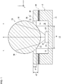
- Fig. 1 is a sectional view illustrating a light-emitting module 10 according to an embodiment.
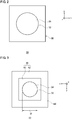
- Fig. 2 is a top view illustrating the structure of a window member 30 of Fig. 1
- Fig. 3 is a bottom view thereof.
- the light-emitting module 10 is provided with a package substrate 12, a light-emitting device 20, a window member 30, and a sealing portion 48.
- the direction of travel of light that is output from the light-emitting module 10 is set to be a z direction, and directions that are perpendicular to the z direction are set to be an x direction and a y direction.
- the z direction is sometimes referred to as a longitudinal direction or a vertical direction, and the x direction and the y direction are each sometimes referred to as a transverse direction or a horizontal direction.
- the package substrate 12 is a plate-like member having an upper surface 14 and a lower surface 15 and is provided with a recessed portion 16 having an opening at the upper surface 14.
- the package substrate 12 is a ceramic substrate containing alumina (Al 2 O 3 ), aluminum nitride (AlN), and the like and is a so-called high temperature co-fired ceramic (HTCC) multilayer substrate.
- the upper surface 14 is rectangular shaped, and, in the central part thereof, the recessed portion 16 forming a rectangular opening is provided. Metallization treatment is performed on a region of the upper surface 14 in which the recessed portion 16 is not provided.
- the upper surface 14 is formed by plating a substrate containing tungsten (W), molybdenum (Mo), etc., with nickel (Ni), gold (Au), or the like. To the upper surface 14, the window member 30 is bonded via the sealing portion 48.
- the lower surface 15 is rectangular shaped, and an external electrode (not shown) that is connected to the anode or cathode of the light-emitting device 20 is provided.
- the recessed portion 16 is open at the upper surface 14 and houses the light-emitting device 20 inside the recessed portion 16.
- the light-emitting device 20 is mounted on a bottom surface 18 of the recessed portion 16.
- the light-emitting device 20 is an LED formed of a compound semiconductor, is housed in the recessed portion 16, and radiates light to the outside of the light-emitting module 10 through the window member 30.
- an ultraviolet light LED is used whose center wavelength or peak wavelength is included in an ultraviolet region of about 200 nm to 360 nm.
- an ultraviolet light LED is used that emits ultraviolet light of around 260 nm, which is a wavelength for high sterilization efficiency.
- AlGaN aluminum gallium nitride
- the light-emitting device 20 has a light-emitting surface 22 and a mounting surface 24 opposite to the light-emitting surface 22.
- the light-emitting device 20 is arranged such that the mounting surface 24 is in contact with the bottom surface 18. This allows heat radiated by the light-emitting device 20 to be dissipated to the outside via the package substrate 12.
- the window member 30 includes a lens portion 32 and a flange portion 38 and is provided on the upper surface 14 such that the window member 30 covers the opening of the recessed portion 16.
- the window member 30 is provided at a position where the lens portion 32 faces the light-emitting device 20 and where a bonding surface 44 of the flange portion 38 faces the upper surface 14.
- the window member 30 is formed of a material that transmits ultraviolet light emitted by the light-emitting device 20 and is formed of, for example, a quartz (SiO 2 ) glass.
- the lens portion 32 is formed into a sphere and functions as a ball lens.
- the lens portion 32 has a light incident surface 34, which faces the light-emitting surface 22 of the light-emitting device 20 and on which light from the light-emitting device 20 becomes incident, and a light emission surface 36, which becomes exposed on the outside of the light-emitting module 10 and which emits light from the light-emitting device 20.
- the light incident surface 34 and the light emission surface 36 are each formed as a spherical surface.
- the lens portion 32 is arranged such that the light-emitting device 20 is located at the focal point of the lens portion 32 and such that the light incident surface 34 becomes close to the light-emitting device 20.
- the lens portion 32 has a collimating function of converting light from the light-emitting device 20 into parallel light and emitting the parallel light.
- the flange unit 38 is a plate-like member that projects in the transverse direction from the lens portion 32 and has an outer circumference in a rectangular shape that corresponds to the package substrate 12.
- the flange portion 38 has a bonding portion 42 facing the upper surface 14 of the package substrate 12 and a connecting portion 40 connecting the lens portion 32 and the bonding portion 42.
- the flange portion 38 is formed integrally with the lens portion 32 and is formed of the same glass material.
- the bonding portion 42 is a part where the bonding surface 44 on which metallization treatment has been performed is formed.
- the bonding surface 44 is formed by a method such as vacuum deposition, sputtering, or the like and is formed of a multilayer film where, for example, titanium (Ti), copper (Cu), nickel (Ni), and gold (Au) are stacked in order on the bonding portion 42 formed of a quartz glass.
- chromium (Cr) may be used instead of titanium.
- the connecting portion 40 is a part where metallization treatment is not performed and is a part where the thickness d1 thereof in the z direction is smaller than the thickness d2 of the bonding portion 42.
- the connecting portion 40 is also considered to be a part where a difference in level is provided away from the upper surface 14 of the package substrate 12. Providing the difference in level on the connecting portion 40 allows the range W of the light incident surface 34, which is a spherical surface, to be increased. Increasing the range W of the light incident surface 34 allows more light output from the light-emitting device 20 to be incident on the light incident surface 34 and allows the amount of light collimated by the lens portion 32 and emitted from the light emission surface 36 to be increased.
- the sealing portion 48 is a sealing material that is provided between the package substrate 12 and the window member 30 and fills a space between the package substrate 12 and the window member 30.
- the sealing portion 48 is formed of a low melting point metal material and contains, for example, a gold-tin (AuSn) or silver-tin (AgSn) alloy.
- AuSn gold-tin
- AgSn silver-tin
- the sealing portion 48 spreads between the upper surface 14 and the bonding surface 44 in a molten state and forms an eutectic bond with the upper surface 14 and the bonding surface 44. Thereby, the sealing portion 48 seals the space between the package substrate 12 and the window member 30.
- the inside of the recessed portion 16 is filled with an inert gas such as nitrogen (N 2 ) or the like.
- the above configuration allows the light-emitting module 10 to encapsulate the light-emitting device 20, which is an ultraviolet light LED, inside the light-emitting module 10 and to output ultraviolet light to the outside via the window member 30.
- Light from the light-emitting device 20 is collected by the lens portion 32 and converted into parallel light or light that is in a condition of being similar to parallel light so as to be emitted. Since a quartz glass is used as the window member 30, even when the light-emitting device 20 that emits ultraviolet light of a wavelength of 360 nm or less is used, the ultraviolet light can be efficiently taken outside.
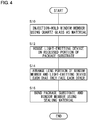
- Fig. 4 is a flowchart illustrating the method of manufacturing the light-emitting module 10.
- the window member 30 is injection molded using a quartz glass as a material (S10), and the light-emitting device 20 is housed in the recessed portion 16 of the package substrate 12 (S12). Then, the window member 30 is arranged over the recessed portion 16 such that the lens portion 32 of the window member 30 faces the light-emitting device 20 (S14), and the upper surface 14 of the package substrate 12 and the bonding surface 44 of the window member 30 are bonded using the sealing material (S16).
- S10 quartz glass as a material
- the window member 30 is molded by preparing a metallic mold corresponding to the shape of the window member 30 including the lens portion 32 and the flange portion 38 and then pouring fused quartz made of quartz glass pellets or the like. After the quartz that has been molded is removed from the metallic mold, residual heat of the quartz is removed, and the surface is polished; thereby, the quartz is processed into the window member 30 made of a transparent quartz glass. Metallization treatment is performed on the bonding surface 44 of the window member 30 that has been polished after the injection molding. In the sealing process of S16, the package substrate 12 and the window member 30 are bonded in a state where the recessed portion 16 of the package substrate 12 is filled with an inert gas such as nitrogen (N 2 ) or the like.
- an inert gas such as nitrogen (N 2 ) or the like.
- the lens portion 32 and the flange portion 38 are formed in an integral manner, and the flange portion 38 allows for bonding to the package substrate 12.
- the sealing properties between the package substrate 12 and the window member 30 can be improved.
- the window member 30 having a lens feature and the package substrate 12 can be directly bonded, the number of bonding sites can be reduced compared to a case where the window member 30 and the package substrate 12 are bonded via another member. Thereby, even when the light-emitting module 10 is to be provided with a lens feature, the number of bonding sites, which are causes for the deterioration of sealing properties, can be reduced, and the reliability of the light-emitting module 10 can be increased.
- the window member 30 is formed of a quartz glass, even when the light-emitting device 20 that emits ultraviolet light of a wavelength of 360 nm or less is used, the ultraviolet light transmittance of the window member 30 can be increased. Further, since the window member 30 is provided with a lens feature, ultraviolet light from the light-emitting device 20 can be efficiently taken out outside. This allows the ultraviolet light output intensity of the light-emitting module 10 to be increased.
- the distance between the light-emitting device 20 and the light incident surface 34 of the lens portion 32 can be reduced compared to a case where a metal frame is inserted between the package substrate 12 and the window member 30. This allows for an increase in the efficiency for taking out ultraviolet light by coupling more ultraviolet light emitted by the light-emitting device 20 at the lens portion 32.
- the bonding to the package substrate 12 is realized using the flange portion 38 having the flat bonding surface 44, a package substrate designed for the bonding to a flat glass plate can be directly used.
- the window member 30 can be bonded to the package substrate 12. Since it is not necessary to newly design or manufacture a package substrate, the cost for the light-emitting module 10 can be lowered.
- the window member 30 having a lens feature can be manufactured by injection molding using a quartz glass, the manufacturing cost can be lowered compared to a case where a base material of a quartz glass is cut and polished for processing. Therefore, a light-emitting module 10 with high sealing properties and reliability and with high output intensity can be realized at a reduced cost.
- the sealing portion 48 formed of a metal material is used for the bonding of the package substrate 12 and the window member 30.
- the wettability of a quartz used as the window member 30 to a low melting point glass is not preferable, and the reliability for sealing may be thus lowered when a low melting point glass is used as the sealing portion.
- the reliability for sealing can be increased.
- the sealing portion 48 a metal that is a material softer than the package substrate 12 and the window member 30 is used. This allows, even when stress is applied due to a difference in the thermal expansion coefficients of respective materials used for the package substrate 12 and the window member 30, the sealing portion 48 to function as a buffer layer that reduces the stress. Thereby, compared to a case where a low melting point glass, which is a relatively hard material, is used as the sealing portion 48, the stress-reducing effect can be improved, and the reliability for sealing can be increased.
- Fig. 5 is a sectional view illustrating a light-emitting module 110 according to an exemplary variation.
- the light-emitting module 110 is different from the above-described embodiment in that a lens portion 132 of a window member 130 has, instead of a spherical shape, a shape that looks like a sphere that has a portion that has been cut off.
- a description will be given in the following mainly regarding differences from the above-described embodiment.
- the window member 130 includes a lens portion 132 and a flange portion 138, and the flange portion 138 has a connecting portion 140 and a bonding portion 142.
- the bonding portion 142 is provided with a bonding surface 144 for bonding to an upper surface 14 of a package substrate 12.
- the lens portion 132 has a light incident surface 134 formed by a spherical surface and a light emission surface 136 formed by a flat surface. Therefore, the lens portion 132 does not project above the flange portion 138 and forms a flat exposed surface along with the flange portion 138.
- the thickness of the light-emitting module 110 in the vertical direction can be made smaller than that of the above-described embodiment, and the light-emitting module 110 can be miniaturized.
- Fig. 6 is a sectional view illustrating a light-emitting module 210 according to an exemplary variation.
- the light-emitting module 210 is different from the above-described first exemplary variation in that a light incident surface 234 of a window member 230 is formed by a Fresnel surface.
- a description will be given in the following mainly regarding differences from the first exemplary variation.
- the window member 230 includes a lens portion 232 and a flange portion 238, and the flange portion 238 has a connecting portion 240 and a bonding portion 242.
- the bonding portion 242 is provided with a bonding surface 244 for bonding to an upper surface 14 of a package substrate 12.
- the lens portion 232 is a so-called Fresnel lens and has a light incident surface 234 formed by a Fresnel surface and a light emission surface 236 formed by a flat surface.
- the lens portion 232 can be arranged closer to a light-emitting device 20, and light from the light-emitting device 20 can be output to the outside more efficiently.
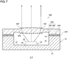
- Fig. 7 is a sectional view illustrating a light-emitting module 310 according to an exemplary variation.
- the light-emitting module 310 is different from the above-described embodiment in that both a light incident surface 334 and a light emission surface 336 of a window member 330 are formed by Fresnel surfaces. A description will be given in the following mainly regarding differences from the embodiment.
- the window member 330 includes a lens portion 332 and a flange portion 338, and the flange portion 338 has a connecting portion 340 and a bonding portion 342.
- the bonding portion 342 is provided with a bonding surface 344 for bonding to an upper surface 14 of a package substrate 12.
- the lens portion 332 is a so-called Fresnel lens, and both the light incident surface 234 and the light emission surface 236 are formed by Fresnel surfaces.
- the light-emitting module 310 can be miniaturized. Further, since the lens portion 232 can be arranged closer to a light-emitting device 20, light from the light-emitting device 20 can be output to the outside more efficiently.
- a quartz glass is used as the material of a window member.
- the material of a window member is not limited to this.
- An optical glass, such as BK7, other than a quartz may be used.
- a resin material such as a transparent plastic may be used as a window member.
- a case is shown where a high temperature co-fired ceramic (HTCC) multilayer substrate is used as a package substrate.
- a low temperature co-fired ceramic (LTCC) multilayer substrate including silica (SiO 2 ), calcium oxide (CaO), boron oxide (B 2 O 3 ), etc., may be used as a ceramic material.
- a material having a relatively low melting point such as copper, silver, or the like may be used instead of a high melting point material such as tungsten, molybdenum, or the like.
- a highly-reliable light-emitting module integrated with a lens feature can be provided.
Landscapes
- Physics & Mathematics (AREA)
- Engineering & Computer Science (AREA)
- General Engineering & Computer Science (AREA)
- General Physics & Mathematics (AREA)
- Optics & Photonics (AREA)
- Led Device Packages (AREA)
Abstract
Description
- The present invention relates to light-emitting modules that seal a light-emitting device therein and a method of manufacturing the light-emitting modules.
- Light-emitting diodes (LED) are used for various purposes such as illumination, signals, and optical communication mainly as light sources for a wavelength range from visible light to infrared light. In general, LED devices are sealed by a light transmissive material for packaging in order to protect light-emitting devices made of compound semiconductors from the external environment.
- A method of the sealing includes a method of coating, with a resin material, light-emitting devices attached to lead electrodes and a method of housing light-emitting devices in a package body provided with an opening and covering the opening with a window member such as a glass plate. The latter method includes a technique of providing a metal frame at the opening of the package body and bonding the metal frame and the glass plate using a low melting point glass. A ball lens for collimating an outgoing beam is sometimes bonded instead of a glass plate (for example, see Patent document No. 1).
- [Patent document No. 1] Japanese Patent Application Publication No.
2002-33519 - In the above-described encapsulating method, since a package body and a ball lens are bonded via a metal frame, the number of parts is increased by the number of metal frames to be prepared, and the number of bonding sites is also increased. While keeping high sealing properties, the package body and the ball lens are desirably bonded with a simpler structure.
- In this background, a purpose of the present invention is to provide a highly-reliable light-emitting module integrated with a lens feature.
- A light-emitting module according to one embodiment of the present invention includes a package substrate that is provided with a recessed portion having an opening at an upper surface thereof; a light-emitting device that is housed in the recessed portion; a window member that is provided on the upper surface such that the window member covers the opening; and a sealing portion that bonds the package substrate and the window member. The window member includes a lens portion facing the light-emitting device and a flange portion that projects from the lens portion and bonds to the sealing portion. The lens portion and the flange portion are formed of the same glass material.
- According to this embodiment, the lens portion and the flange portion are formed in an integral manner, and the flange portion allows for bonding to the package substrate. Thus, the sealing properties between the package substrate and the window member can be improved. Further, since the window member having a lens feature and the package substrate can be directly bonded, the number of bonding sites can be reduced compared to a case where the window member and the package substrate are bonded via another member. Thereby, even when the window member having a lens feature is bonded, the number of bonding sites, which are causes for the deterioration of sealing properties, can be reduced, and the reliability of the light-emitting module can be increased.
- The lens portion and the flange portion may be formed of a quartz glass.
- The light-emitting device may emit ultraviolet light whose wavelength is included in the band of a wavelength of 200 nm to 360 nm.
- The lens portion may convert light from the light-emitting device into parallel light and emit the parallel light to the outside.
- The lens portion may be a sphere or a portion of a sphere.
- The lens portion may be a Fresnel lens.
- Another embodiment of the present invention relates to a method of manufacturing a light-emitting module. This method includes: injection-molding a window member including a lens portion and a flange portion projecting from the lens portion, using fused quartz as a material; housing a light-emitting device in a recessed portion of a package substrate that is provided with the recessed portion having an opening at an upper surface thereof; arranging the window member at the upper surface such that the lens portion and the light-emitting device face each other; and bonding the package substrate and the flange portion using a sealing material.
- According to this embodiment, since a window member having a lens portion and a flange portion can be formed in an integral manner by injection molding, the manufacturing cost for a light-emitting module can be lowered compared to a case where a base material of a quartz glass is cut and polished to form a window member.
- According to the present invention, a highly-reliable light-emitting module integrated with a lens feature can be provided.
-
-
Fig. 1 is a sectional view illustrating a light-emitting module according to an embodiment; -
Fig. 2 is a top view illustrating the structure of a window member ofFig. 1 ; -
Fig. 3 is a bottom view illustrating the structure of the window member ofFig. 1 ; -
Fig. 4 is a flowchart illustrating a method of manufacturing a light-emitting module; -
Fig. 5 is a sectional view illustrating a light-emitting module according to an exemplary variation; -
Fig. 6 is a sectional view illustrating a light-emitting module according to an exemplary variation; and -
Fig. 7 is a sectional view illustrating a light-emitting module according to an exemplary variation. - Described below is an explanation of the embodiments of the present invention with reference to figures. In the figures, like numerals represent like constituting elements, and the description thereof is omitted appropriately.
-
Fig. 1 is a sectional view illustrating a light-emittingmodule 10 according to an embodiment.Fig. 2 is a top view illustrating the structure of awindow member 30 ofFig. 1 , andFig. 3 is a bottom view thereof. The light-emitting module 10 is provided with apackage substrate 12, a light-emitting device 20, awindow member 30, and asealing portion 48. - In the explanation of the present specification, the direction of travel of light that is output from the light-
emitting module 10 is set to be a z direction, and directions that are perpendicular to the z direction are set to be an x direction and a y direction. The z direction is sometimes referred to as a longitudinal direction or a vertical direction, and the x direction and the y direction are each sometimes referred to as a transverse direction or a horizontal direction. - The
package substrate 12 is a plate-like member having anupper surface 14 and alower surface 15 and is provided with a recessedportion 16 having an opening at theupper surface 14. Thepackage substrate 12 is a ceramic substrate containing alumina (Al2O3), aluminum nitride (AlN), and the like and is a so-called high temperature co-fired ceramic (HTCC) multilayer substrate. - The
upper surface 14 is rectangular shaped, and, in the central part thereof, therecessed portion 16 forming a rectangular opening is provided. Metallization treatment is performed on a region of theupper surface 14 in which therecessed portion 16 is not provided. Theupper surface 14 is formed by plating a substrate containing tungsten (W), molybdenum (Mo), etc., with nickel (Ni), gold (Au), or the like. To theupper surface 14, thewindow member 30 is bonded via the sealingportion 48. - The
lower surface 15 is rectangular shaped, and an external electrode (not shown) that is connected to the anode or cathode of the light-emittingdevice 20 is provided. Therecessed portion 16 is open at theupper surface 14 and houses the light-emittingdevice 20 inside the recessedportion 16. The light-emittingdevice 20 is mounted on abottom surface 18 of the recessedportion 16. - The light-
emitting device 20 is an LED formed of a compound semiconductor, is housed in therecessed portion 16, and radiates light to the outside of the light-emittingmodule 10 through thewindow member 30. In the present embodiment, as the light-emitting device 20, an ultraviolet light LED is used whose center wavelength or peak wavelength is included in an ultraviolet region of about 200 nm to 360 nm. For example, an ultraviolet light LED is used that emits ultraviolet light of around 260 nm, which is a wavelength for high sterilization efficiency. As such an ultraviolet light LED, for example, those in which aluminum gallium nitride (AlGaN) is used are known. - The light-
emitting device 20 has a light-emittingsurface 22 and amounting surface 24 opposite to the light-emittingsurface 22. The light-emittingdevice 20 is arranged such that themounting surface 24 is in contact with thebottom surface 18. This allows heat radiated by the light-emittingdevice 20 to be dissipated to the outside via thepackage substrate 12. - The
window member 30 includes alens portion 32 and aflange portion 38 and is provided on theupper surface 14 such that thewindow member 30 covers the opening of therecessed portion 16. Thewindow member 30 is provided at a position where thelens portion 32 faces the light-emitting device 20 and where abonding surface 44 of theflange portion 38 faces theupper surface 14. Thewindow member 30 is formed of a material that transmits ultraviolet light emitted by the light-emittingdevice 20 and is formed of, for example, a quartz (SiO2) glass. - The
lens portion 32 is formed into a sphere and functions as a ball lens. Thelens portion 32 has alight incident surface 34, which faces the light-emittingsurface 22 of the light-emittingdevice 20 and on which light from the light-emittingdevice 20 becomes incident, and alight emission surface 36, which becomes exposed on the outside of the light-emittingmodule 10 and which emits light from the light-emittingdevice 20. Thelight incident surface 34 and thelight emission surface 36 are each formed as a spherical surface. Thelens portion 32 is arranged such that the light-emittingdevice 20 is located at the focal point of thelens portion 32 and such that thelight incident surface 34 becomes close to the light-emittingdevice 20. Thus, thelens portion 32 has a collimating function of converting light from the light-emittingdevice 20 into parallel light and emitting the parallel light. - The
flange unit 38 is a plate-like member that projects in the transverse direction from thelens portion 32 and has an outer circumference in a rectangular shape that corresponds to thepackage substrate 12. Theflange portion 38 has abonding portion 42 facing theupper surface 14 of thepackage substrate 12 and a connectingportion 40 connecting thelens portion 32 and thebonding portion 42. Theflange portion 38 is formed integrally with thelens portion 32 and is formed of the same glass material. - The
bonding portion 42 is a part where thebonding surface 44 on which metallization treatment has been performed is formed. Thebonding surface 44 is formed by a method such as vacuum deposition, sputtering, or the like and is formed of a multilayer film where, for example, titanium (Ti), copper (Cu), nickel (Ni), and gold (Au) are stacked in order on thebonding portion 42 formed of a quartz glass. Alternatively, chromium (Cr) may be used instead of titanium. - The connecting
portion 40 is a part where metallization treatment is not performed and is a part where the thickness d1 thereof in the z direction is smaller than the thickness d2 of thebonding portion 42. The connectingportion 40 is also considered to be a part where a difference in level is provided away from theupper surface 14 of thepackage substrate 12. Providing the difference in level on the connectingportion 40 allows the range W of thelight incident surface 34, which is a spherical surface, to be increased. Increasing the range W of thelight incident surface 34 allows more light output from the light-emittingdevice 20 to be incident on thelight incident surface 34 and allows the amount of light collimated by thelens portion 32 and emitted from thelight emission surface 36 to be increased. - The sealing
portion 48 is a sealing material that is provided between thepackage substrate 12 and thewindow member 30 and fills a space between thepackage substrate 12 and thewindow member 30. The sealingportion 48 is formed of a low melting point metal material and contains, for example, a gold-tin (AuSn) or silver-tin (AgSn) alloy. The sealingportion 48 spreads between theupper surface 14 and thebonding surface 44 in a molten state and forms an eutectic bond with theupper surface 14 and thebonding surface 44. Thereby, the sealingportion 48 seals the space between thepackage substrate 12 and thewindow member 30. At the time of the sealing, the inside of the recessedportion 16 is filled with an inert gas such as nitrogen (N2) or the like. - The above configuration allows the light-emitting
module 10 to encapsulate the light-emittingdevice 20, which is an ultraviolet light LED, inside the light-emittingmodule 10 and to output ultraviolet light to the outside via thewindow member 30. Light from the light-emittingdevice 20 is collected by thelens portion 32 and converted into parallel light or light that is in a condition of being similar to parallel light so as to be emitted. Since a quartz glass is used as thewindow member 30, even when the light-emittingdevice 20 that emits ultraviolet light of a wavelength of 360 nm or less is used, the ultraviolet light can be efficiently taken outside. - An explanation will be given now regarding a method of manufacturing the light-emitting
module 10.Fig. 4 is a flowchart illustrating the method of manufacturing the light-emittingmodule 10. Thewindow member 30 is injection molded using a quartz glass as a material (S10), and the light-emittingdevice 20 is housed in the recessedportion 16 of the package substrate 12 (S12). Then, thewindow member 30 is arranged over the recessedportion 16 such that thelens portion 32 of thewindow member 30 faces the light-emitting device 20 (S14), and theupper surface 14 of thepackage substrate 12 and thebonding surface 44 of thewindow member 30 are bonded using the sealing material (S16). - In the injection molding process of S12, the
window member 30 is molded by preparing a metallic mold corresponding to the shape of thewindow member 30 including thelens portion 32 and theflange portion 38 and then pouring fused quartz made of quartz glass pellets or the like. After the quartz that has been molded is removed from the metallic mold, residual heat of the quartz is removed, and the surface is polished; thereby, the quartz is processed into thewindow member 30 made of a transparent quartz glass. Metallization treatment is performed on thebonding surface 44 of thewindow member 30 that has been polished after the injection molding. In the sealing process of S16, thepackage substrate 12 and thewindow member 30 are bonded in a state where the recessedportion 16 of thepackage substrate 12 is filled with an inert gas such as nitrogen (N2) or the like. - Shown below are advantageous effects achieved by the light-emitting
module 10 according to the present embodiment. - According to the present embodiment, the
lens portion 32 and theflange portion 38 are formed in an integral manner, and theflange portion 38 allows for bonding to thepackage substrate 12. Thus, the sealing properties between thepackage substrate 12 and thewindow member 30 can be improved. Further, since thewindow member 30 having a lens feature and thepackage substrate 12 can be directly bonded, the number of bonding sites can be reduced compared to a case where thewindow member 30 and thepackage substrate 12 are bonded via another member. Thereby, even when the light-emittingmodule 10 is to be provided with a lens feature, the number of bonding sites, which are causes for the deterioration of sealing properties, can be reduced, and the reliability of the light-emittingmodule 10 can be increased. - According to the present embodiment, since the
window member 30 is formed of a quartz glass, even when the light-emittingdevice 20 that emits ultraviolet light of a wavelength of 360 nm or less is used, the ultraviolet light transmittance of thewindow member 30 can be increased. Further, since thewindow member 30 is provided with a lens feature, ultraviolet light from the light-emittingdevice 20 can be efficiently taken out outside. This allows the ultraviolet light output intensity of the light-emittingmodule 10 to be increased. - In the present embodiment, since a structure is employed where no metal frame is provided for the bonding of the
package substrate 12 and thewindow member 30, the distance between the light-emittingdevice 20 and thelight incident surface 34 of thelens portion 32 can be reduced compared to a case where a metal frame is inserted between thepackage substrate 12 and thewindow member 30. This allows for an increase in the efficiency for taking out ultraviolet light by coupling more ultraviolet light emitted by the light-emittingdevice 20 at thelens portion 32. - According to the present embodiment, since the bonding to the
package substrate 12 is realized using theflange portion 38 having theflat bonding surface 44, a package substrate designed for the bonding to a flat glass plate can be directly used. In other words, without changing the design of thepackage substrate 12 in order to be bonded to thewindow member 30 having a lens feature, thewindow member 30 can be bonded to thepackage substrate 12. Since it is not necessary to newly design or manufacture a package substrate, the cost for the light-emittingmodule 10 can be lowered. - According to the present embodiment, since the
window member 30 having a lens feature can be manufactured by injection molding using a quartz glass, the manufacturing cost can be lowered compared to a case where a base material of a quartz glass is cut and polished for processing. Therefore, a light-emittingmodule 10 with high sealing properties and reliability and with high output intensity can be realized at a reduced cost. - In the present embodiment, instead of a low melting point glass, the sealing
portion 48 formed of a metal material is used for the bonding of thepackage substrate 12 and thewindow member 30. In general, the wettability of a quartz used as thewindow member 30 to a low melting point glass is not preferable, and the reliability for sealing may be thus lowered when a low melting point glass is used as the sealing portion. On the other hand, in the present embodiment, since thewindow member 30 on which metallization treatment has been performed is sealed using a metal material with high wettability, the reliability for sealing can be increased. - In the present embodiment, as the sealing
portion 48, a metal that is a material softer than thepackage substrate 12 and thewindow member 30 is used. This allows, even when stress is applied due to a difference in the thermal expansion coefficients of respective materials used for thepackage substrate 12 and thewindow member 30, the sealingportion 48 to function as a buffer layer that reduces the stress. Thereby, compared to a case where a low melting point glass, which is a relatively hard material, is used as the sealingportion 48, the stress-reducing effect can be improved, and the reliability for sealing can be increased. -
Fig. 5 is a sectional view illustrating a light-emittingmodule 110 according to an exemplary variation. The light-emittingmodule 110 is different from the above-described embodiment in that alens portion 132 of awindow member 130 has, instead of a spherical shape, a shape that looks like a sphere that has a portion that has been cut off. A description will be given in the following mainly regarding differences from the above-described embodiment. - The
window member 130 includes alens portion 132 and aflange portion 138, and theflange portion 138 has a connectingportion 140 and abonding portion 142. Thebonding portion 142 is provided with abonding surface 144 for bonding to anupper surface 14 of apackage substrate 12. Thelens portion 132 has alight incident surface 134 formed by a spherical surface and alight emission surface 136 formed by a flat surface. Therefore, thelens portion 132 does not project above theflange portion 138 and forms a flat exposed surface along with theflange portion 138. Therefore, according to the present exemplary variation, since thelight emission surface 136 of thelens portion 132 is formed by a flat surface, the thickness of the light-emittingmodule 110 in the vertical direction can be made smaller than that of the above-described embodiment, and the light-emittingmodule 110 can be miniaturized. -
Fig. 6 is a sectional view illustrating a light-emittingmodule 210 according to an exemplary variation. The light-emittingmodule 210 is different from the above-described first exemplary variation in that alight incident surface 234 of awindow member 230 is formed by a Fresnel surface. A description will be given in the following mainly regarding differences from the first exemplary variation. - The
window member 230 includes alens portion 232 and aflange portion 238, and theflange portion 238 has a connectingportion 240 and abonding portion 242. Thebonding portion 242 is provided with abonding surface 244 for bonding to anupper surface 14 of apackage substrate 12. Thelens portion 232 is a so-called Fresnel lens and has alight incident surface 234 formed by a Fresnel surface and alight emission surface 236 formed by a flat surface. According to the present exemplary variation, since the thickness in the vertical direction is smaller than that of thelens portion 132 according to the above-described exemplary variation, thelens portion 232 can be arranged closer to a light-emittingdevice 20, and light from the light-emittingdevice 20 can be output to the outside more efficiently. -
Fig. 7 is a sectional view illustrating a light-emittingmodule 310 according to an exemplary variation. The light-emittingmodule 310 is different from the above-described embodiment in that both alight incident surface 334 and alight emission surface 336 of awindow member 330 are formed by Fresnel surfaces. A description will be given in the following mainly regarding differences from the embodiment. - The
window member 330 includes alens portion 332 and aflange portion 338, and theflange portion 338 has a connectingportion 340 and abonding portion 342. Thebonding portion 342 is provided with abonding surface 344 for bonding to anupper surface 14 of apackage substrate 12. Thelens portion 332 is a so-called Fresnel lens, and both thelight incident surface 234 and thelight emission surface 236 are formed by Fresnel surfaces. - According to the present exemplary variation, since the thickness in the vertical direction can be made smaller than that of the
lens portion 32 according to the above-described embodiment, the light-emittingmodule 310 can be miniaturized. Further, since thelens portion 232 can be arranged closer to a light-emittingdevice 20, light from the light-emittingdevice 20 can be output to the outside more efficiently. - These embodiments are intended to be illustrative only, and it will be obvious to those skilled in the art that various modifications could be developed based on the knowledge of a skilled person and that such modifications are also within the scope of the present invention.
- In the above stated embodiment and exemplary variations, a case is shown where those that emit ultraviolet light are used as light-emitting devices. Alternatively, a light-emitting device that emits visible light and/or infrared light may be used.
- In the above stated embodiment and exemplary variations, a case is shown where a quartz glass is used as the material of a window member. However, the material of a window member is not limited to this. An optical glass, such as BK7, other than a quartz may be used. Alternatively, a resin material such as a transparent plastic may be used as a window member.
- In the above stated embodiment and exemplary variations, a case is shown where a high temperature co-fired ceramic (HTCC) multilayer substrate is used as a package substrate. Alternatively, a low temperature co-fired ceramic (LTCC) multilayer substrate including silica (SiO2), calcium oxide (CaO), boron oxide (B2O3), etc., may be used as a ceramic material. In this case, as metallization treatment performed on an
upper surface 14, a material having a relatively low melting point such as copper, silver, or the like may be used instead of a high melting point material such as tungsten, molybdenum, or the like. -
- 10
- light-emitting module
- 12
- package substrate
- 14
- upper surface
- 16
- recessed portion
- 20
- light-emitting device
- 30
- window member
- 32
- lens portion
- 38
- flange portion
- 48
- sealing portion
- According to the present invention, a highly-reliable light-emitting module integrated with a lens feature can be provided.
Claims (7)
- A light-emitting module comprising:a package substrate that is provided with a recessed portion having an opening at an upper surface thereof;a light-emitting device that is housed in the recessed portion;a window member that is provided on the upper surface such that the window member covers the opening; anda sealing portion that bonds the package substrate and the window member,wherein the window member includes a lens portion facing the light-emitting device and a flange portion that projects from the lens portion and bonds to the sealing portion, andwherein the lens portion and the flange portion are formed of the same glass material.
- The light-emitting module according to claim 1,
wherein the lens portion and the flange portion are formed of a quartz glass. - The light-emitting module according to claim 2,
wherein the light-emitting device emits ultraviolet light whose wavelength is included in the band of a wavelength of 200 nm to 360 nm. - The light-emitting module according to any one of claims 1 to 3, wherein the lens portion converts light from the light-emitting device into parallel light and emits the parallel light to the outside.
- The light-emitting module according to claim 4,
wherein the lens portion is a sphere or a portion of a sphere. - The light-emitting module according to claim 4,
wherein the lens portion is a Fresnel lens. - A method of manufacturing a light-emitting module comprising:injection-molding a window member including a lens portion and a flange portion projecting from the lens portion, using fused quartz as a material;housing a light-emitting device in a recessed portion of a package substrate that is provided with the recessed portion having an opening at an upper surface thereof;arranging the window member at the upper surface such that the lens portion and the light-emitting device face each other; andbonding the package substrate and the flange portion using a sealing material.
Applications Claiming Priority (2)
| Application Number | Priority Date | Filing Date | Title |
|---|---|---|---|
| JP2015184169A JP6668022B2 (en) | 2015-09-17 | 2015-09-17 | Light emitting module and method of manufacturing light emitting module |
| PCT/JP2016/075012 WO2017047358A1 (en) | 2015-09-17 | 2016-08-26 | Light emitting module and method for manufacturing light emitting module |
Publications (3)
| Publication Number | Publication Date |
|---|---|
| EP3352231A1 true EP3352231A1 (en) | 2018-07-25 |
| EP3352231A4 EP3352231A4 (en) | 2019-02-13 |
| EP3352231B1 EP3352231B1 (en) | 2020-09-09 |
Family
ID=58289112
Family Applications (1)
| Application Number | Title | Priority Date | Filing Date |
|---|---|---|---|
| EP16846229.9A Active EP3352231B1 (en) | 2015-09-17 | 2016-08-26 | Light emitting module and method for manufacturing light emitting module |
Country Status (5)
| Country | Link |
|---|---|
| US (1) | US10883680B2 (en) |
| EP (1) | EP3352231B1 (en) |
| JP (1) | JP6668022B2 (en) |
| CN (1) | CN108140704B (en) |
| WO (1) | WO2017047358A1 (en) |
Cited By (1)
| Publication number | Priority date | Publication date | Assignee | Title |
|---|---|---|---|---|
| EP3467885A4 (en) * | 2016-06-01 | 2020-01-22 | Shin-Etsu Quartz Products Co., Ltd. | SILICA GLASS ELEMENT FOR SEALING A ULTRAVIOLET SMD LED ELEMENT AND METHOD FOR MANUFACTURING A QUARTZ GLASS ELEMENT FOR ULTRAVIOLET LED |
Families Citing this family (15)
| Publication number | Priority date | Publication date | Assignee | Title |
|---|---|---|---|---|
| JP2017216389A (en) * | 2016-06-01 | 2017-12-07 | 信越石英株式会社 | Silica glass member for hermetic seal of ultraviolet smd type led element |
| WO2019038846A1 (en) * | 2017-08-23 | 2019-02-28 | 日本碍子株式会社 | Method for producing optical component, and method for producing transparent sealing member |
| JP6644745B2 (en) * | 2017-08-25 | 2020-02-12 | エーディーワイ株式会社 | Ultraviolet light element, package for ultraviolet light element, optical member used for ultraviolet light element, and method of manufacturing the optical member |
| JP6871184B2 (en) * | 2018-01-31 | 2021-05-12 | 日機装株式会社 | Manufacturing method of semiconductor light emitting device |
| JP7107692B2 (en) * | 2018-02-13 | 2022-07-27 | スタンレー電気株式会社 | Light source package and light source package manufacturing method |
| JP7239804B2 (en) | 2018-08-31 | 2023-03-15 | 日亜化学工業株式会社 | LENS, LIGHT-EMITTING DEVICE AND MANUFACTURING METHOD THEREOF |
| JP6897641B2 (en) | 2018-08-31 | 2021-07-07 | 日亜化学工業株式会社 | Lenses and light emitting devices and their manufacturing methods |
| JP7206475B2 (en) | 2018-08-31 | 2023-01-18 | 日亜化学工業株式会社 | LENS, LIGHT-EMITTING DEVICE AND MANUFACTURING METHOD THEREOF |
| JP7288172B2 (en) | 2018-09-26 | 2023-06-07 | 日亜化学工業株式会社 | Light source device and manufacturing method thereof |
| CN109309154B (en) * | 2018-10-12 | 2020-05-19 | 京东方科技集团股份有限公司 | Display unit, display substrate, preparation method of display substrate and display device |
| JP7252820B2 (en) * | 2019-04-12 | 2023-04-05 | 日機装株式会社 | Semiconductor light emitting device and manufacturing method thereof |
| CN113394320B (en) | 2020-03-11 | 2023-04-07 | 隆达电子股份有限公司 | Light emitting diode packaging structure |
| JP7500317B2 (en) * | 2020-07-22 | 2024-06-17 | スタンレー電気株式会社 | Semiconductor light emitting device |
| CN115702504B (en) | 2020-12-25 | 2025-12-12 | 阔斯泰有限责任公司 | Silicon dioxide components and LED devices |
| CN113113524A (en) * | 2021-03-30 | 2021-07-13 | 佛山市国星光电股份有限公司 | Deep ultraviolet LED device and manufacturing method thereof |
Family Cites Families (31)
| Publication number | Priority date | Publication date | Assignee | Title |
|---|---|---|---|---|
| JPS637674A (en) * | 1986-06-27 | 1988-01-13 | Mitsubishi Electric Corp | Light emitting diode |
| JP2002033519A (en) | 2000-07-14 | 2002-01-31 | Sumitomo Electric Ind Ltd | Optical communication package, window member thereof, and method of manufacturing the same |
| JP2005038956A (en) * | 2003-07-17 | 2005-02-10 | Matsushita Electric Ind Co Ltd | Optical component and manufacturing method thereof |
| JP3898721B2 (en) * | 2004-01-28 | 2007-03-28 | 京セラ株式会社 | Light emitting device and lighting device |
| JP2005235864A (en) | 2004-02-17 | 2005-09-02 | Hamamatsu Photonics Kk | Optical semiconductor device |
| JP4471685B2 (en) * | 2004-03-10 | 2010-06-02 | シチズン電子株式会社 | Lighting device |
| US7105875B2 (en) * | 2004-06-03 | 2006-09-12 | Wide Bandgap, Llc | Lateral power diodes |
| KR100576866B1 (en) * | 2004-06-16 | 2006-05-10 | 삼성전기주식회사 | Light emitting diode and manufacturing method |
| KR100662844B1 (en) * | 2005-06-10 | 2007-01-02 | 삼성전자주식회사 | LED package and manufacturing method thereof and LED array module using same |
| US7758204B2 (en) * | 2006-01-26 | 2010-07-20 | Brasscorp Limited | LED spotlight |
| JP5130680B2 (en) * | 2006-03-02 | 2013-01-30 | 日亜化学工業株式会社 | Semiconductor device and method for forming the same |
| JP5041732B2 (en) * | 2006-05-16 | 2012-10-03 | アルプス電気株式会社 | Luminescent body and manufacturing method thereof |
| CN200990388Y (en) * | 2006-09-30 | 2007-12-12 | 东贝光电科技股份有限公司 | Light emitting element |
| CN101302079A (en) * | 2007-05-09 | 2008-11-12 | 深圳富泰宏精密工业有限公司 | Coated glass, coating system for preparing the same and coating method |
| TWI351115B (en) * | 2007-05-18 | 2011-10-21 | Everlight Electronics Co Ltd | Light-emitting diode module and the manufacturing method thereof |
| US20100237378A1 (en) * | 2009-03-19 | 2010-09-23 | Tzu-Han Lin | Light emitting diode package structure and fabrication thereof |
| JP2012028436A (en) * | 2010-07-21 | 2012-02-09 | Seiko Instruments Inc | Light emitting device and manufacturing method thereof |
| DE102010046088A1 (en) * | 2010-09-20 | 2012-03-22 | Osram Opto Semiconductors Gmbh | Housing and method of manufacturing a housing |
| JP2012109475A (en) * | 2010-11-19 | 2012-06-07 | Rohm Co Ltd | Light emitting device, manufacturing method of light emitting device, and optical device |
| CN202111088U (en) * | 2011-05-31 | 2012-01-11 | 宁波市鄞州雷迈半导体科技有限公司 | Packaging structure of high power LED chip |
| KR101959035B1 (en) * | 2011-10-31 | 2019-03-18 | 서울바이오시스 주식회사 | Light emitting diode package and method of fabricating the same |
| JP2013105140A (en) * | 2011-11-16 | 2013-05-30 | Olympus Corp | Method of manufacturing optical element, microstructure forming mold, and microstructure forming mold assembly |
| DE102012200327B4 (en) * | 2012-01-11 | 2022-01-05 | Osram Gmbh | Optoelectronic component |
| US9240524B2 (en) * | 2012-03-05 | 2016-01-19 | Seoul Viosys Co., Ltd. | Light-emitting device and method of manufacturing the same |
| US9263658B2 (en) * | 2012-03-05 | 2016-02-16 | Seoul Viosys Co., Ltd. | Light-emitting device and method of manufacturing the same |
| KR101516358B1 (en) * | 2012-03-06 | 2015-05-04 | 삼성전자주식회사 | Light Emitting Device |
| JP6048880B2 (en) | 2013-01-25 | 2016-12-21 | パナソニックIpマネジメント株式会社 | LIGHT EMITTING ELEMENT PACKAGE AND LIGHT EMITTING DEVICE USING THE SAME |
| US9799802B2 (en) * | 2013-05-23 | 2017-10-24 | Lg Innotek Co., Ltd. | Light emitting module |
| CN204088315U (en) * | 2014-08-26 | 2015-01-07 | 北京大学东莞光电研究院 | MCOB LED fluorescent powder separate package structure |
| EP3038173B1 (en) * | 2014-12-23 | 2019-05-22 | LG Innotek Co., Ltd. | Light emitting device |
| US9895459B2 (en) * | 2015-10-21 | 2018-02-20 | Stanley Electric Co., Ltd. | Ultraviolet ray emitting package having resin adhesive layer and ultraviolet ray irradiating apparatus |
-
2015
- 2015-09-17 JP JP2015184169A patent/JP6668022B2/en active Active
-
2016
- 2016-08-26 WO PCT/JP2016/075012 patent/WO2017047358A1/en not_active Ceased
- 2016-08-26 CN CN201680050639.8A patent/CN108140704B/en active Active
- 2016-08-26 EP EP16846229.9A patent/EP3352231B1/en active Active
-
2018
- 2018-03-05 US US15/912,043 patent/US10883680B2/en active Active
Cited By (1)
| Publication number | Priority date | Publication date | Assignee | Title |
|---|---|---|---|---|
| EP3467885A4 (en) * | 2016-06-01 | 2020-01-22 | Shin-Etsu Quartz Products Co., Ltd. | SILICA GLASS ELEMENT FOR SEALING A ULTRAVIOLET SMD LED ELEMENT AND METHOD FOR MANUFACTURING A QUARTZ GLASS ELEMENT FOR ULTRAVIOLET LED |
Also Published As
| Publication number | Publication date |
|---|---|
| EP3352231A4 (en) | 2019-02-13 |
| US20180195677A1 (en) | 2018-07-12 |
| CN108140704A (en) | 2018-06-08 |
| EP3352231B1 (en) | 2020-09-09 |
| JP6668022B2 (en) | 2020-03-18 |
| CN108140704B (en) | 2021-03-16 |
| WO2017047358A1 (en) | 2017-03-23 |
| JP2017059716A (en) | 2017-03-23 |
| US10883680B2 (en) | 2021-01-05 |
Similar Documents
| Publication | Publication Date | Title |
|---|---|---|
| EP3352231B1 (en) | Light emitting module and method for manufacturing light emitting module | |
| US11222998B2 (en) | Optical semiconductor apparatus and method of manufacturing optical semiconductor apparatus | |
| JP2015018873A (en) | Semiconductor module | |
| US11217730B2 (en) | Optical semiconductor apparatus and method of manufacturing optical semiconductor apparatus | |
| CN109690796B (en) | Optical semiconductor device and method for manufacturing optical semiconductor device | |
| KR101516358B1 (en) | Light Emitting Device | |
| EP3001466B1 (en) | Light-emitting module | |
| CN104937733B (en) | Method and optoelectronic device for fabricating a plurality of optoelectronic devices | |
| JP2006237609A (en) | Semiconductor light emitting device and manufacturing method thereof | |
| CN101789482A (en) | Solid element device and method for manufacture thereof | |
| JP7348570B2 (en) | light emitting device | |
| US10622523B2 (en) | Light-emitting diode and method of producing a light-emitting diode | |
| JP2015018872A (en) | Window member, semiconductor module and window member manufacturing method | |
| US8178890B2 (en) | Light emitting diode package structure | |
| US20220376156A1 (en) | Semiconductor device | |
| US10847699B2 (en) | Optical semiconductor apparatus | |
| US12191628B2 (en) | Semiconductor light emitting device | |
| JP4820133B2 (en) | Light emitting device | |
| KR102369978B1 (en) | A light emitting device package | |
| US20250006543A1 (en) | Method for producing an optoelectronic assembly |
Legal Events
| Date | Code | Title | Description |
|---|---|---|---|
| STAA | Information on the status of an ep patent application or granted ep patent |
Free format text: STATUS: THE INTERNATIONAL PUBLICATION HAS BEEN MADE |
|
| PUAI | Public reference made under article 153(3) epc to a published international application that has entered the european phase |
Free format text: ORIGINAL CODE: 0009012 |
|
| STAA | Information on the status of an ep patent application or granted ep patent |
Free format text: STATUS: REQUEST FOR EXAMINATION WAS MADE |
|
| 17P | Request for examination filed |
Effective date: 20180329 |
|
| AK | Designated contracting states |
Kind code of ref document: A1 Designated state(s): AL AT BE BG CH CY CZ DE DK EE ES FI FR GB GR HR HU IE IS IT LI LT LU LV MC MK MT NL NO PL PT RO RS SE SI SK SM TR |
|
| AX | Request for extension of the european patent |
Extension state: BA ME |
|
| DAV | Request for validation of the european patent (deleted) | ||
| DAX | Request for extension of the european patent (deleted) | ||
| A4 | Supplementary search report drawn up and despatched |
Effective date: 20190114 |
|
| RIC1 | Information provided on ipc code assigned before grant |
Ipc: H01L 33/60 20100101ALI20190108BHEP Ipc: H01L 33/48 20100101ALI20190108BHEP Ipc: H01L 33/58 20100101AFI20190108BHEP |
|
| GRAP | Despatch of communication of intention to grant a patent |
Free format text: ORIGINAL CODE: EPIDOSNIGR1 |
|
| STAA | Information on the status of an ep patent application or granted ep patent |
Free format text: STATUS: GRANT OF PATENT IS INTENDED |
|
| INTG | Intention to grant announced |
Effective date: 20191025 |
|
| GRAS | Grant fee paid |
Free format text: ORIGINAL CODE: EPIDOSNIGR3 |
|
| GRAJ | Information related to disapproval of communication of intention to grant by the applicant or resumption of examination proceedings by the epo deleted |
Free format text: ORIGINAL CODE: EPIDOSDIGR1 |
|
| GRAL | Information related to payment of fee for publishing/printing deleted |
Free format text: ORIGINAL CODE: EPIDOSDIGR3 |
|
| STAA | Information on the status of an ep patent application or granted ep patent |
Free format text: STATUS: REQUEST FOR EXAMINATION WAS MADE |
|
| GRAJ | Information related to disapproval of communication of intention to grant by the applicant or resumption of examination proceedings by the epo deleted |
Free format text: ORIGINAL CODE: EPIDOSDIGR1 |
|
| GRAL | Information related to payment of fee for publishing/printing deleted |
Free format text: ORIGINAL CODE: EPIDOSDIGR3 |
|
| GRAP | Despatch of communication of intention to grant a patent |
Free format text: ORIGINAL CODE: EPIDOSNIGR1 |
|
| STAA | Information on the status of an ep patent application or granted ep patent |
Free format text: STATUS: GRANT OF PATENT IS INTENDED |
|
| INTC | Intention to grant announced (deleted) | ||
| INTG | Intention to grant announced |
Effective date: 20200226 |
|
| GRAA | (expected) grant |
Free format text: ORIGINAL CODE: 0009210 |
|
| STAA | Information on the status of an ep patent application or granted ep patent |
Free format text: STATUS: THE PATENT HAS BEEN GRANTED |
|
| AK | Designated contracting states |
Kind code of ref document: B1 Designated state(s): AL AT BE BG CH CY CZ DE DK EE ES FI FR GB GR HR HU IE IS IT LI LT LU LV MC MK MT NL NO PL PT RO RS SE SI SK SM TR |
|
| REG | Reference to a national code |
Ref country code: GB Ref legal event code: FG4D |
|
| REG | Reference to a national code |
Ref country code: AT Ref legal event code: REF Ref document number: 1312662 Country of ref document: AT Kind code of ref document: T Effective date: 20200915 Ref country code: CH Ref legal event code: EP |
|
| REG | Reference to a national code |
Ref country code: DE Ref legal event code: R096 Ref document number: 602016043867 Country of ref document: DE |
|
| REG | Reference to a national code |
Ref country code: IE Ref legal event code: FG4D |
|
| REG | Reference to a national code |
Ref country code: LT Ref legal event code: MG4D |
|
| PG25 | Lapsed in a contracting state [announced via postgrant information from national office to epo] |
Ref country code: BG Free format text: LAPSE BECAUSE OF FAILURE TO SUBMIT A TRANSLATION OF THE DESCRIPTION OR TO PAY THE FEE WITHIN THE PRESCRIBED TIME-LIMIT Effective date: 20201209 Ref country code: SE Free format text: LAPSE BECAUSE OF FAILURE TO SUBMIT A TRANSLATION OF THE DESCRIPTION OR TO PAY THE FEE WITHIN THE PRESCRIBED TIME-LIMIT Effective date: 20200909 Ref country code: NO Free format text: LAPSE BECAUSE OF FAILURE TO SUBMIT A TRANSLATION OF THE DESCRIPTION OR TO PAY THE FEE WITHIN THE PRESCRIBED TIME-LIMIT Effective date: 20201209 Ref country code: HR Free format text: LAPSE BECAUSE OF FAILURE TO SUBMIT A TRANSLATION OF THE DESCRIPTION OR TO PAY THE FEE WITHIN THE PRESCRIBED TIME-LIMIT Effective date: 20200909 Ref country code: FI Free format text: LAPSE BECAUSE OF FAILURE TO SUBMIT A TRANSLATION OF THE DESCRIPTION OR TO PAY THE FEE WITHIN THE PRESCRIBED TIME-LIMIT Effective date: 20200909 Ref country code: LT Free format text: LAPSE BECAUSE OF FAILURE TO SUBMIT A TRANSLATION OF THE DESCRIPTION OR TO PAY THE FEE WITHIN THE PRESCRIBED TIME-LIMIT Effective date: 20200909 Ref country code: GR Free format text: LAPSE BECAUSE OF FAILURE TO SUBMIT A TRANSLATION OF THE DESCRIPTION OR TO PAY THE FEE WITHIN THE PRESCRIBED TIME-LIMIT Effective date: 20201210 |
|
| REG | Reference to a national code |
Ref country code: AT Ref legal event code: MK05 Ref document number: 1312662 Country of ref document: AT Kind code of ref document: T Effective date: 20200909 |
|
| REG | Reference to a national code |
Ref country code: NL Ref legal event code: MP Effective date: 20200909 |
|
| PG25 | Lapsed in a contracting state [announced via postgrant information from national office to epo] |
Ref country code: LV Free format text: LAPSE BECAUSE OF FAILURE TO SUBMIT A TRANSLATION OF THE DESCRIPTION OR TO PAY THE FEE WITHIN THE PRESCRIBED TIME-LIMIT Effective date: 20200909 Ref country code: PL Free format text: LAPSE BECAUSE OF FAILURE TO SUBMIT A TRANSLATION OF THE DESCRIPTION OR TO PAY THE FEE WITHIN THE PRESCRIBED TIME-LIMIT Effective date: 20200909 Ref country code: RS Free format text: LAPSE BECAUSE OF FAILURE TO SUBMIT A TRANSLATION OF THE DESCRIPTION OR TO PAY THE FEE WITHIN THE PRESCRIBED TIME-LIMIT Effective date: 20200909 |
|
| PG25 | Lapsed in a contracting state [announced via postgrant information from national office to epo] |
Ref country code: EE Free format text: LAPSE BECAUSE OF FAILURE TO SUBMIT A TRANSLATION OF THE DESCRIPTION OR TO PAY THE FEE WITHIN THE PRESCRIBED TIME-LIMIT Effective date: 20200909 Ref country code: SM Free format text: LAPSE BECAUSE OF FAILURE TO SUBMIT A TRANSLATION OF THE DESCRIPTION OR TO PAY THE FEE WITHIN THE PRESCRIBED TIME-LIMIT Effective date: 20200909 Ref country code: PT Free format text: LAPSE BECAUSE OF FAILURE TO SUBMIT A TRANSLATION OF THE DESCRIPTION OR TO PAY THE FEE WITHIN THE PRESCRIBED TIME-LIMIT Effective date: 20210111 Ref country code: RO Free format text: LAPSE BECAUSE OF FAILURE TO SUBMIT A TRANSLATION OF THE DESCRIPTION OR TO PAY THE FEE WITHIN THE PRESCRIBED TIME-LIMIT Effective date: 20200909 Ref country code: CZ Free format text: LAPSE BECAUSE OF FAILURE TO SUBMIT A TRANSLATION OF THE DESCRIPTION OR TO PAY THE FEE WITHIN THE PRESCRIBED TIME-LIMIT Effective date: 20200909 |
|
| PG25 | Lapsed in a contracting state [announced via postgrant information from national office to epo] |
Ref country code: IS Free format text: LAPSE BECAUSE OF FAILURE TO SUBMIT A TRANSLATION OF THE DESCRIPTION OR TO PAY THE FEE WITHIN THE PRESCRIBED TIME-LIMIT Effective date: 20210109 Ref country code: AT Free format text: LAPSE BECAUSE OF FAILURE TO SUBMIT A TRANSLATION OF THE DESCRIPTION OR TO PAY THE FEE WITHIN THE PRESCRIBED TIME-LIMIT Effective date: 20200909 Ref country code: AL Free format text: LAPSE BECAUSE OF FAILURE TO SUBMIT A TRANSLATION OF THE DESCRIPTION OR TO PAY THE FEE WITHIN THE PRESCRIBED TIME-LIMIT Effective date: 20200909 Ref country code: ES Free format text: LAPSE BECAUSE OF FAILURE TO SUBMIT A TRANSLATION OF THE DESCRIPTION OR TO PAY THE FEE WITHIN THE PRESCRIBED TIME-LIMIT Effective date: 20200909 |
|
| REG | Reference to a national code |
Ref country code: DE Ref legal event code: R097 Ref document number: 602016043867 Country of ref document: DE |
|
| PG25 | Lapsed in a contracting state [announced via postgrant information from national office to epo] |
Ref country code: SK Free format text: LAPSE BECAUSE OF FAILURE TO SUBMIT A TRANSLATION OF THE DESCRIPTION OR TO PAY THE FEE WITHIN THE PRESCRIBED TIME-LIMIT Effective date: 20200909 |
|
| PLBE | No opposition filed within time limit |
Free format text: ORIGINAL CODE: 0009261 |
|
| STAA | Information on the status of an ep patent application or granted ep patent |
Free format text: STATUS: NO OPPOSITION FILED WITHIN TIME LIMIT |
|
| 26N | No opposition filed |
Effective date: 20210610 |
|
| PG25 | Lapsed in a contracting state [announced via postgrant information from national office to epo] |
Ref country code: SI Free format text: LAPSE BECAUSE OF FAILURE TO SUBMIT A TRANSLATION OF THE DESCRIPTION OR TO PAY THE FEE WITHIN THE PRESCRIBED TIME-LIMIT Effective date: 20200909 Ref country code: DK Free format text: LAPSE BECAUSE OF FAILURE TO SUBMIT A TRANSLATION OF THE DESCRIPTION OR TO PAY THE FEE WITHIN THE PRESCRIBED TIME-LIMIT Effective date: 20200909 |
|
| PG25 | Lapsed in a contracting state [announced via postgrant information from national office to epo] |
Ref country code: IT Free format text: LAPSE BECAUSE OF FAILURE TO SUBMIT A TRANSLATION OF THE DESCRIPTION OR TO PAY THE FEE WITHIN THE PRESCRIBED TIME-LIMIT Effective date: 20200909 |
|
| REG | Reference to a national code |
Ref country code: CH Ref legal event code: PL |
|
| PG25 | Lapsed in a contracting state [announced via postgrant information from national office to epo] |
Ref country code: MC Free format text: LAPSE BECAUSE OF FAILURE TO SUBMIT A TRANSLATION OF THE DESCRIPTION OR TO PAY THE FEE WITHIN THE PRESCRIBED TIME-LIMIT Effective date: 20200909 |
|
| REG | Reference to a national code |
Ref country code: BE Ref legal event code: MM Effective date: 20210831 |
|
| GBPC | Gb: european patent ceased through non-payment of renewal fee |
Effective date: 20210826 |
|
| PG25 | Lapsed in a contracting state [announced via postgrant information from national office to epo] |
Ref country code: LI Free format text: LAPSE BECAUSE OF NON-PAYMENT OF DUE FEES Effective date: 20210831 Ref country code: CH Free format text: LAPSE BECAUSE OF NON-PAYMENT OF DUE FEES Effective date: 20210831 |
|
| PG25 | Lapsed in a contracting state [announced via postgrant information from national office to epo] |
Ref country code: LU Free format text: LAPSE BECAUSE OF NON-PAYMENT OF DUE FEES Effective date: 20210826 |
|
| PG25 | Lapsed in a contracting state [announced via postgrant information from national office to epo] |
Ref country code: IE Free format text: LAPSE BECAUSE OF NON-PAYMENT OF DUE FEES Effective date: 20210826 Ref country code: GB Free format text: LAPSE BECAUSE OF NON-PAYMENT OF DUE FEES Effective date: 20210826 Ref country code: FR Free format text: LAPSE BECAUSE OF NON-PAYMENT OF DUE FEES Effective date: 20210831 Ref country code: BE Free format text: LAPSE BECAUSE OF NON-PAYMENT OF DUE FEES Effective date: 20210831 |
|
| PG25 | Lapsed in a contracting state [announced via postgrant information from national office to epo] |
Ref country code: HU Free format text: LAPSE BECAUSE OF FAILURE TO SUBMIT A TRANSLATION OF THE DESCRIPTION OR TO PAY THE FEE WITHIN THE PRESCRIBED TIME-LIMIT; INVALID AB INITIO Effective date: 20160826 |
|
| PG25 | Lapsed in a contracting state [announced via postgrant information from national office to epo] |
Ref country code: NL Free format text: LAPSE BECAUSE OF NON-PAYMENT OF DUE FEES Effective date: 20200923 Ref country code: CY Free format text: LAPSE BECAUSE OF FAILURE TO SUBMIT A TRANSLATION OF THE DESCRIPTION OR TO PAY THE FEE WITHIN THE PRESCRIBED TIME-LIMIT Effective date: 20200909 |
|
| PG25 | Lapsed in a contracting state [announced via postgrant information from national office to epo] |
Ref country code: MK Free format text: LAPSE BECAUSE OF FAILURE TO SUBMIT A TRANSLATION OF THE DESCRIPTION OR TO PAY THE FEE WITHIN THE PRESCRIBED TIME-LIMIT Effective date: 20200909 |
|
| PG25 | Lapsed in a contracting state [announced via postgrant information from national office to epo] |
Ref country code: TR Free format text: LAPSE BECAUSE OF FAILURE TO SUBMIT A TRANSLATION OF THE DESCRIPTION OR TO PAY THE FEE WITHIN THE PRESCRIBED TIME-LIMIT Effective date: 20200909 |
|
| PG25 | Lapsed in a contracting state [announced via postgrant information from national office to epo] |
Ref country code: MT Free format text: LAPSE BECAUSE OF FAILURE TO SUBMIT A TRANSLATION OF THE DESCRIPTION OR TO PAY THE FEE WITHIN THE PRESCRIBED TIME-LIMIT Effective date: 20200909 |
|
| REG | Reference to a national code |
Ref country code: DE Ref legal event code: R079 Ref document number: 602016043867 Country of ref document: DE Free format text: PREVIOUS MAIN CLASS: H01L0033580000 Ipc: H10H0020855000 |
|
| PGFP | Annual fee paid to national office [announced via postgrant information from national office to epo] |
Ref country code: DE Payment date: 20250820 Year of fee payment: 10 |