EP3352225A1 - Semiconductor device and method of manufacturing same, electric power converting device, three-phase motor system, automobile and railway vehicle - Google Patents
Semiconductor device and method of manufacturing same, electric power converting device, three-phase motor system, automobile and railway vehicle Download PDFInfo
- Publication number
- EP3352225A1 EP3352225A1 EP15904057.5A EP15904057A EP3352225A1 EP 3352225 A1 EP3352225 A1 EP 3352225A1 EP 15904057 A EP15904057 A EP 15904057A EP 3352225 A1 EP3352225 A1 EP 3352225A1
- Authority
- EP
- European Patent Office
- Prior art keywords
- region
- type
- semiconductor
- semiconductor device
- end surface
- Prior art date
- Legal status (The legal status is an assumption and is not a legal conclusion. Google has not performed a legal analysis and makes no representation as to the accuracy of the status listed.)
- Granted
Links
Images





Classifications
-
- H—ELECTRICITY
- H10—SEMICONDUCTOR DEVICES; ELECTRIC SOLID-STATE DEVICES NOT OTHERWISE PROVIDED FOR
- H10D—INORGANIC ELECTRIC SEMICONDUCTOR DEVICES
- H10D30/00—Field-effect transistors [FET]
- H10D30/60—Insulated-gate field-effect transistors [IGFET]
- H10D30/64—Double-diffused metal-oxide semiconductor [DMOS] FETs
- H10D30/66—Vertical DMOS [VDMOS] FETs
- H10D30/665—Vertical DMOS [VDMOS] FETs having edge termination structures
-
- B—PERFORMING OPERATIONS; TRANSPORTING
- B60—VEHICLES IN GENERAL
- B60L—PROPULSION OF ELECTRICALLY-PROPELLED VEHICLES; SUPPLYING ELECTRIC POWER FOR AUXILIARY EQUIPMENT OF ELECTRICALLY-PROPELLED VEHICLES; ELECTRODYNAMIC BRAKE SYSTEMS FOR VEHICLES IN GENERAL; MAGNETIC SUSPENSION OR LEVITATION FOR VEHICLES; MONITORING OPERATING VARIABLES OF ELECTRICALLY-PROPELLED VEHICLES; ELECTRIC SAFETY DEVICES FOR ELECTRICALLY-PROPELLED VEHICLES
- B60L15/00—Methods, circuits, or devices for controlling the traction-motor speed of electrically-propelled vehicles
-
- H—ELECTRICITY
- H02—GENERATION; CONVERSION OR DISTRIBUTION OF ELECTRIC POWER
- H02P—CONTROL OR REGULATION OF ELECTRIC MOTORS, ELECTRIC GENERATORS OR DYNAMO-ELECTRIC CONVERTERS; CONTROLLING TRANSFORMERS, REACTORS OR CHOKE COILS
- H02P27/00—Arrangements or methods for the control of AC motors characterised by the kind of supply voltage
- H02P27/04—Arrangements or methods for the control of AC motors characterised by the kind of supply voltage using variable-frequency supply voltage, e.g. inverter or converter supply voltage
- H02P27/06—Arrangements or methods for the control of AC motors characterised by the kind of supply voltage using variable-frequency supply voltage, e.g. inverter or converter supply voltage using DC to AC converters or inverters
-
- H—ELECTRICITY
- H10—SEMICONDUCTOR DEVICES; ELECTRIC SOLID-STATE DEVICES NOT OTHERWISE PROVIDED FOR
- H10D—INORGANIC ELECTRIC SEMICONDUCTOR DEVICES
- H10D12/00—Bipolar devices controlled by the field effect, e.g. insulated-gate bipolar transistors [IGBT]
- H10D12/01—Manufacture or treatment
- H10D12/031—Manufacture or treatment of IGBTs
-
- H—ELECTRICITY
- H10—SEMICONDUCTOR DEVICES; ELECTRIC SOLID-STATE DEVICES NOT OTHERWISE PROVIDED FOR
- H10D—INORGANIC ELECTRIC SEMICONDUCTOR DEVICES
- H10D30/00—Field-effect transistors [FET]
- H10D30/01—Manufacture or treatment
- H10D30/021—Manufacture or treatment of FETs having insulated gates [IGFET]
- H10D30/028—Manufacture or treatment of FETs having insulated gates [IGFET] of double-diffused metal oxide semiconductor [DMOS] FETs
- H10D30/0291—Manufacture or treatment of FETs having insulated gates [IGFET] of double-diffused metal oxide semiconductor [DMOS] FETs of vertical DMOS [VDMOS] FETs
-
- H—ELECTRICITY
- H10—SEMICONDUCTOR DEVICES; ELECTRIC SOLID-STATE DEVICES NOT OTHERWISE PROVIDED FOR
- H10D—INORGANIC ELECTRIC SEMICONDUCTOR DEVICES
- H10D62/00—Semiconductor bodies, or regions thereof, of devices having potential barriers
- H10D62/10—Shapes, relative sizes or dispositions of the regions of the semiconductor bodies; Shapes of the semiconductor bodies
- H10D62/102—Constructional design considerations for preventing surface leakage or controlling electric field concentration
- H10D62/103—Constructional design considerations for preventing surface leakage or controlling electric field concentration for increasing or controlling the breakdown voltage of reverse-biased devices
- H10D62/105—Constructional design considerations for preventing surface leakage or controlling electric field concentration for increasing or controlling the breakdown voltage of reverse-biased devices by having particular doping profiles, shapes or arrangements of PN junctions; by having supplementary regions, e.g. junction termination extension [JTE]
-
- H—ELECTRICITY
- H10—SEMICONDUCTOR DEVICES; ELECTRIC SOLID-STATE DEVICES NOT OTHERWISE PROVIDED FOR
- H10D—INORGANIC ELECTRIC SEMICONDUCTOR DEVICES
- H10D62/00—Semiconductor bodies, or regions thereof, of devices having potential barriers
- H10D62/10—Shapes, relative sizes or dispositions of the regions of the semiconductor bodies; Shapes of the semiconductor bodies
- H10D62/102—Constructional design considerations for preventing surface leakage or controlling electric field concentration
- H10D62/103—Constructional design considerations for preventing surface leakage or controlling electric field concentration for increasing or controlling the breakdown voltage of reverse-biased devices
- H10D62/105—Constructional design considerations for preventing surface leakage or controlling electric field concentration for increasing or controlling the breakdown voltage of reverse-biased devices by having particular doping profiles, shapes or arrangements of PN junctions; by having supplementary regions, e.g. junction termination extension [JTE]
- H10D62/106—Constructional design considerations for preventing surface leakage or controlling electric field concentration for increasing or controlling the breakdown voltage of reverse-biased devices by having particular doping profiles, shapes or arrangements of PN junctions; by having supplementary regions, e.g. junction termination extension [JTE] having supplementary regions doped oppositely to or in rectifying contact with regions of the semiconductor bodies, e.g. guard rings with PN or Schottky junctions
- H10D62/107—Buried supplementary regions, e.g. buried guard rings
-
- H—ELECTRICITY
- H10—SEMICONDUCTOR DEVICES; ELECTRIC SOLID-STATE DEVICES NOT OTHERWISE PROVIDED FOR
- H10D—INORGANIC ELECTRIC SEMICONDUCTOR DEVICES
- H10D62/00—Semiconductor bodies, or regions thereof, of devices having potential barriers
- H10D62/10—Shapes, relative sizes or dispositions of the regions of the semiconductor bodies; Shapes of the semiconductor bodies
- H10D62/102—Constructional design considerations for preventing surface leakage or controlling electric field concentration
- H10D62/103—Constructional design considerations for preventing surface leakage or controlling electric field concentration for increasing or controlling the breakdown voltage of reverse-biased devices
- H10D62/105—Constructional design considerations for preventing surface leakage or controlling electric field concentration for increasing or controlling the breakdown voltage of reverse-biased devices by having particular doping profiles, shapes or arrangements of PN junctions; by having supplementary regions, e.g. junction termination extension [JTE]
- H10D62/109—Reduced surface field [RESURF] PN junction structures
-
- H—ELECTRICITY
- H10—SEMICONDUCTOR DEVICES; ELECTRIC SOLID-STATE DEVICES NOT OTHERWISE PROVIDED FOR
- H10D—INORGANIC ELECTRIC SEMICONDUCTOR DEVICES
- H10D62/00—Semiconductor bodies, or regions thereof, of devices having potential barriers
- H10D62/10—Shapes, relative sizes or dispositions of the regions of the semiconductor bodies; Shapes of the semiconductor bodies
- H10D62/102—Constructional design considerations for preventing surface leakage or controlling electric field concentration
- H10D62/112—Constructional design considerations for preventing surface leakage or controlling electric field concentration for preventing surface leakage due to surface inversion layers, e.g. by using channel stoppers
-
- H—ELECTRICITY
- H10—SEMICONDUCTOR DEVICES; ELECTRIC SOLID-STATE DEVICES NOT OTHERWISE PROVIDED FOR
- H10D—INORGANIC ELECTRIC SEMICONDUCTOR DEVICES
- H10D62/00—Semiconductor bodies, or regions thereof, of devices having potential barriers
- H10D62/10—Shapes, relative sizes or dispositions of the regions of the semiconductor bodies; Shapes of the semiconductor bodies
- H10D62/17—Semiconductor regions connected to electrodes not carrying current to be rectified, amplified or switched, e.g. channel regions
- H10D62/393—Body regions of DMOS transistors or IGBTs
-
- H—ELECTRICITY
- H10—SEMICONDUCTOR DEVICES; ELECTRIC SOLID-STATE DEVICES NOT OTHERWISE PROVIDED FOR
- H10D—INORGANIC ELECTRIC SEMICONDUCTOR DEVICES
- H10D62/00—Semiconductor bodies, or regions thereof, of devices having potential barriers
- H10D62/80—Semiconductor bodies, or regions thereof, of devices having potential barriers characterised by the materials
- H10D62/83—Semiconductor bodies, or regions thereof, of devices having potential barriers characterised by the materials being Group IV materials, e.g. B-doped Si or undoped Ge
- H10D62/832—Semiconductor bodies, or regions thereof, of devices having potential barriers characterised by the materials being Group IV materials, e.g. B-doped Si or undoped Ge being Group IV materials comprising two or more elements, e.g. SiGe
- H10D62/8325—Silicon carbide
-
- H—ELECTRICITY
- H10—SEMICONDUCTOR DEVICES; ELECTRIC SOLID-STATE DEVICES NOT OTHERWISE PROVIDED FOR
- H10D—INORGANIC ELECTRIC SEMICONDUCTOR DEVICES
- H10D62/00—Semiconductor bodies, or regions thereof, of devices having potential barriers
- H10D62/80—Semiconductor bodies, or regions thereof, of devices having potential barriers characterised by the materials
- H10D62/83—Semiconductor bodies, or regions thereof, of devices having potential barriers characterised by the materials being Group IV materials, e.g. B-doped Si or undoped Ge
- H10D62/834—Semiconductor bodies, or regions thereof, of devices having potential barriers characterised by the materials being Group IV materials, e.g. B-doped Si or undoped Ge further characterised by the dopants
-
- H—ELECTRICITY
- H10—SEMICONDUCTOR DEVICES; ELECTRIC SOLID-STATE DEVICES NOT OTHERWISE PROVIDED FOR
- H10D—INORGANIC ELECTRIC SEMICONDUCTOR DEVICES
- H10D84/00—Integrated devices formed in or on semiconductor substrates that comprise only semiconducting layers, e.g. on Si wafers or on GaAs-on-Si wafers
- H10D84/101—Integrated devices comprising main components and built-in components, e.g. IGBT having built-in freewheel diode
- H10D84/141—VDMOS having built-in components
- H10D84/143—VDMOS having built-in components the built-in components being PN junction diodes
- H10D84/144—VDMOS having built-in components the built-in components being PN junction diodes in antiparallel diode configurations
-
- H—ELECTRICITY
- H10—SEMICONDUCTOR DEVICES; ELECTRIC SOLID-STATE DEVICES NOT OTHERWISE PROVIDED FOR
- H10P—GENERIC PROCESSES OR APPARATUS FOR THE MANUFACTURE OR TREATMENT OF DEVICES COVERED BY CLASS H10
- H10P30/00—Ion implantation into wafers, substrates or parts of devices
- H10P30/20—Ion implantation into wafers, substrates or parts of devices into semiconductor materials, e.g. for doping
- H10P30/22—Ion implantation into wafers, substrates or parts of devices into semiconductor materials, e.g. for doping using masks
-
- B—PERFORMING OPERATIONS; TRANSPORTING
- B60—VEHICLES IN GENERAL
- B60L—PROPULSION OF ELECTRICALLY-PROPELLED VEHICLES; SUPPLYING ELECTRIC POWER FOR AUXILIARY EQUIPMENT OF ELECTRICALLY-PROPELLED VEHICLES; ELECTRODYNAMIC BRAKE SYSTEMS FOR VEHICLES IN GENERAL; MAGNETIC SUSPENSION OR LEVITATION FOR VEHICLES; MONITORING OPERATING VARIABLES OF ELECTRICALLY-PROPELLED VEHICLES; ELECTRIC SAFETY DEVICES FOR ELECTRICALLY-PROPELLED VEHICLES
- B60L2200/00—Type of vehicles
- B60L2200/26—Rail vehicles
Definitions
- the present invention relates to a semiconductor device and a method of manufacturing the same, a power converter, a three-phase motor system, an automobile, and a railway vehicle.
- Patent Literature 1 Japanese Unexamined Patent Application Publication No. 2012-59870.
- This publication describes a semiconductor device including: a first wide bandgap semiconductor region of a first conductivity type; a second wide bandgap semiconductor region of a second conductivity type formed so as to be sandwiched between the first semiconductor regions; and a plurality of third wide bandgap semiconductor regions of the second conductivity type, each of which is formed so as to be at least partially connected to the second semiconductor region and to be sandwiched between the first semiconductor regions.
- the width of wide bandgap semiconductor layer of the first conductivity type is d
- the interval between the third semiconductor regions is 2d ⁇ tan 18° or more.
- Patent Literature 1 Japanese Unexamined Patent Application Publication No. 2012-59870
- SiC-MOSFET Metal Oxide Semiconductor Field Effect Transistor
- SiC silicon carbide
- a breakdown field higher than Si silicon
- a freewheeling diode is provided outside the SiC-MOSFET in order to suppress the leakage current in the backward operation by reducing the electric field on the interface (Schottky interface) between metal and semiconductor when a voltage is applied in the opposite direction.
- a freewheeling diode is incorporated into a substrate in which SiC-MOSFET is formed.
- the body diode the built-in freewheeling diode
- Energization deterioration is a phenomenon such as an increase in the on-resistance which is the resistance in the energization of the SiC-MOSFET. The greater the on-resistance, the greater the loss and the more heat is generated, which affects the life or performance of the power module.
- Crystal defects of SiC which are mainly stacking faults and micro defects as the origin of the stacking faults, are present in a manufactured SiC wafer.
- a large number of stacking faults also occur starting from defects occurring in the dicing surface in dicing of the SiC wafer.
- the crystal defects present in the manufactured SiC wafer can be reduced by improving the SiC wafer itself as well as the epitaxial growth on the SiC wafer.
- the semiconductor device includes: an n - -type epitaxial layer formed on a main surface of an n + -type SiC substrate; a p-type termination region annularly formed in the n - -type epitaxial layer outside an active region; and an n-type hole annihilation region annularly formed in the n - type epitaxial layer outside a p-type termination region, apart from the p type termination region.
- the n-type hole annihilation region has a first end surface facing a p-type termination region as well as a second end surface on the opposite side of the first end surface.
- the present invention it is possible to suppress energization deterioration due to crystal defects in a semiconductor device including SiC-MOSFET.
- the number of elements when referring to the number of elements (including the number of pieces, numerical value, amount, range, and the like), the number of elements is not limited to a specific number unless expressly stated otherwise and unless the number is clearly limited to a specific number in principle or other reasons. The number of elements can be greater or smaller than the specific number.
- Fig. 1 is a fragmentary plan view showing an example of the semiconductor device (semiconductor chip) according to the first embodiment.
- Fig. 2 is a fragmentary cross-sectional view showing an example of SiC-MOSFET according to the first embodiment (which is a cross-sectional view taken along line A-A shown in Fig. 1 ).
- the SiC-MOSFET is MOSFET of planar type DMOS (Double diffused Metal Oxide Semiconductor) structure.
- Fig. 3 is a fragmentary cross-sectional view showing an enlarged part of the end portion of the semiconductor device (semiconductor chip) according to the first embodiment (which is a cross-sectional view taken along line B-B shown in Fig. 1 ).
- a semiconductor device (a semiconductor chip) 1 is configured with an active region (element formation region, activation region) 2 through which current mainly flows, and a peripheral region 3 formed around the active region 2 in a plan view.
- a termination structure of, for example, p + -type semiconductor region 4 and p-type termination region (termination) 5 is formed in the peripheral region 3.
- the p-type termination region 5 is formed so as to surround the p + -type semiconductor region 4.
- the p-type termination region 5 includes, for example, a junction termination extension (JTE) structure having a single- or multi-stage concentration distribution.
- an n-type hole annihilation region 6 is formed apart from the p-type termination region 5 on the side of the outer periphery (peripheral portion, end portion) of the semiconductor device 1 than the peripheral region 3.
- the n-type hole annihilation region 6 also has a function as a channel stopper.
- the outer periphery of the semiconductor device 1 is a dicing surface 7 that is formed in dicing for cutting a plurality of semiconductor chips from a semiconductor wafer.
- Fig. 2 shows an example of the structure of the SiC-MOSFET formed in the active region 2.
- An n-type buffer layer 12 composed of SiC with an impurity concentration lower than the impurity concentration of an n + -type SiC substrate 11 is formed on a surface (first main surface) of the n + -type SiC substrate 11 composed of SiC. Then, an n - -type epitaxial layer 13 composed of SiC with an impurity concentration lower than the impurity concentration of the n-type buffer layer 12 is formed on the upper surface of the n-type buffer layer 12.
- the n-type buffer layer 12 is formed by an epitaxial growth method similarly to the n - -type epitaxial layer 13.
- the n-type buffer layer 12 can also be formed by an ion implantation method.
- the thickness of the n-type buffer layer 12 is, for example, about 3 to 20 ⁇ m
- the thickness of the n - -type epitaxial layer 13 is, for example, about 5 to 50 ⁇ m.
- the n-type buffer 12 is formed in the first embodiment, but it may also be possible to directly form the n - -type epitaxial layer 13 on the surface of the n + -type SiC substrate 11, without forming the n-buffer layer 12.
- a plurality of p-type body regions (well regions) 14 are formed apart from each other within the n - -type epitaxial layer 13, with a predetermined depth from the upper surface of the n - -type epitaxial layer 13.
- the depth of the p-type body region 14 from the upper surface of the n - -type epitaxial layer 13 is, for example, about 0.5 to 2 ⁇ m.
- n + -type source region 15 is formed within the p-type body region 14, with a predetermined depth from the upper surface of the n - -type epitaxial layer 13.
- the n + -type source region 15 is formed within the p-type body region 14, apart from the end surface of the p-type body region 14.
- the depth of the n + -type source region 15 from the upper surface of the n - -type epitaxial layer 13 is, for example, about 0.05 to 0.5 ⁇ m.
- a p + -type potential fixing region 16 for fixing the potential of the p-type body region 14 is formed within the p-type body region 14, with a predetermined depth from the upper surface of the n - -type epitaxial layer 13.
- the depth of the p + -type potential fixing region 16 from the upper surface of the n - -type epitaxial layer 13 is, for example, about 0.05 to 0.5 ⁇ m.
- the region sandwiched between adjacent p-type body regions 14 is the portion that functions as a JFET (Junction Field Effect Transistor) region (doped region) 17.
- the p-type body region 4 which is located between the end surface of the p-type body region 14 (the interface between the JFET region 17 and the p-type body region 14) and the end surface of the n + -type source region 15 (the interface between the p-type body region 14 and the n + -type source region 15), is the portion that functions as a channel region 18.
- the region in which the p-type body region 14 and the JFET region 17 are not formed is a region that functions as an n - drift layer for enhancing the breakdown voltage. Further, the n + -type SiC substrate 11 is a region that functions as a drain layer.
- a built-in diode namely, a body diode DI is formed which includes the p + -type potential fixing region 16, the p-type body region 14, the n - -type epitaxial layer 13, the n-type buffer layer 12, and the n + -type SiC substrate 11, between a source wiring electrode 24 and a drain wiring electrode 16.
- the preferred impurity concentration range of the n + -type SiC substrate 11 is, for example, about 1 ⁇ 10 18 to 1 ⁇ 10 21 cm -3
- the preferred impurity concentration range of the n-type buffer layer 12 is, for example, about 1 ⁇ 10 17 to 1 ⁇ 10 19 cm -3
- the preferred impurity concentration range of the n - -type epitaxial layer 13 is, for example, about 1 ⁇ 10 14 to 1 ⁇ 10 16 cm -3 .
- the preferred impurity concentration range of the p-type body region 14 is, for example, about 1 ⁇ 10 17 to 1 ⁇ 10 18 cm -3
- the preferred impurity concentration range of the n + -type source region 15 is, for example, about 1 ⁇ 10 19 to 1 ⁇ 10 20 cm -3
- the preferred impurity concentration range of the p + -type potential fixing region 16 is, for example, about 1 ⁇ 10 19 to 1 ⁇ 10 20 cm -3
- the preferred impurity concentration range of the JFET region 17 is, for example, about 3 ⁇ 10 16 cm -3 .
- the preferred impurity concentration region of the p + -type semiconductor region 4 is, for example, about 1 ⁇ 10 19 to 1 ⁇ 10 20 cm -3
- the preferred impurity concentration region of the p-type termination region 5 is, for example, about 1 ⁇ 10 17 to 1 ⁇ 10 18 cm -3 .
- a gate insulating film 19 is formed over the channel region 18, and a gate electrode 20 is formed over the gate insulating film 19.
- the gate electrode 20 is formed in a band shape in a plan view.
- the p-type body region 14 is formed between adjacent gate electrodes 20 that are spaced apart from each other.
- the layout of the SiC-MOSFET is not limited to this.
- the gate electrode 20 is formed in a lattice pattern in a plan view and then the p-type body region 14 is formed to be surrounded by the gate electrode 20.
- the gate insulating film 19 and the gate electrode 20 are covered by an interlayer insulating film 21.
- Part of the n + -type source region 15 as well as the p + -type potential fixing region 16 are exposed in the bottom of an opening 22 formed in the interlayer insulating film 21. Note that a metal silicide layer may be formed on these surfaces.
- part of the n + -type source region 15 as well as the p + -type potential fixing region 16 are electrically connected to the source wiring electrode 24.
- the gate electrode 20 is electrically connected to the gate wiring electrode.
- the back surface (second main surface) of the n + -type SiC substrate 11 is electrically connected to the drain wiring electrode 26.
- a metal silicide layer may be formed on the back surface of the n + -type SiC substrate 11.
- Fig. 3 shows an example of the arrangement of the p-type termination region 5 and the n-type hole annihilation region 6, both of which are formed in the end portion of the semiconductor device 1.
- the n-type hole annihilation region 6 is formed apart from the p-type termination region 5 and also apart from the outer periphery of the semiconductor device 1, around the p-type termination region 5 in a plan view.
- the outer periphery of the semiconductor device 1 is the dicing surface 7 that is formed in dicing process in which a plurality of semiconductor chips are cut out of a semiconductor wafer.
- the position of the dicing surface 7 of the semiconductor device 1 is referred to as X 0
- the position of the end surface of the n-type hole annihilation region 6 that faces the p-type termination region 5 is referred to as X NR
- the distance between the dicing surface 7 of the semiconductor device 1 and the end surface of the n-type hole annihilation region 6 that faces the p-type termination region 5 is referred to as
- the n-type hole annihilation region 6 has a predetermined width (L NR ) in a plan view.
- the width (L NR ) is set smaller than
- the width (L NR ) of the n-type hole annihilation region 6 can be, for example, about 1 ⁇ m.
- the distance between the p-type termination region 5 and the n-type hole annihilation region 6 is set according to the breakdown voltage of the semiconductor device 1 in such a way that the depletion layer end extending from the p-type termination region 5 at the time of non-energization (off state) does not reaches the n-type hole annihilation region 6 and punch-through does not occur.
- the n-type hole annihilation region 6 has a predetermined depth (d NR ) from the upper surface of the n - -type epitaxial layer 13.
- the depth (d NR ) is equal to or more than the depth (d TM ) of the p-type termination region 5, which is located at a position closest to the n-type hole annihilation region 6, from the upper surface of the n - -type epitaxial layer 13.
- the depth (d NR ) of the n-type hole annihilation region 6 can be, for example, about 0.5 ⁇ m.
- the n-type hole annihilation region 6 is formed in such a way that the sum of the distance (
- a semiconductor wafer in which many semiconductor chips are formed is cut along scribe regions (also referred to as dicing regions or cutting margins) provided on the four sides of each of the semiconductor chips, and is separated into individual semiconductor chips.
- scribe regions also referred to as dicing regions or cutting margins
- a defect occurs in the dicing surface of the semiconductor chip, and a number of stacking faults occur within the SiC crystal starting from the defect occurring in the dicing surface.
- the present inventors conducted an ultraviolet irradiation experiment on the semiconductor chip after dicing.
- the present inventors have studied the relationship between holes and defects that occur in the dicing surface, by taking advantage of the phenomenon that when holes induced by ultraviolet light within the SiC crystal recombine with electrons in stacking faults or in micro defects which are the origin of the stacking faults, these defects are extended and the incident light intensity is increased.
- Ultraviolet light was emitted obliquely from above the semiconductor chip.
- the n-type hole annihilation region 6 was provided between the p-type termination region 5 and the dicing surface 7 of the semiconductor device 1 in such a way that the holes supplied in the energization did not reach the dicing surface 7 of the semiconductor device 1.
- the defects are further extended by the energy emitted by the recombination of holes and electrons, and as a result, a number of stacking faults occur in the n - -type epitaxial layer 13.
- the n-type hole annihilation region 6 is provided, the holes are recombined and disappear in the n-type hole annihilation region 6 and do not reach the dicing surface 7 of the semiconductor device 1, so that it is possible to suppress the recombination of holes and electrons in the defects occurred in the dicing surface 7 of the semiconductor device 1.
- the power module and the power converter can be miniaturized.
- Patent Literature 1 describes the fact that the concentration of the holes diffusing in the range of 18 degrees in the normal direction of the lower surface of a p + -type propagation region is particularly high, and that the concentration of the holes diffusing in the range of 22 degrees is increased. Further as described, for example, in the paragraph [0093] of Japanese Unexamined Patent Application Publication No. 2009-392510 , there is a possibility that holes will diffuse at the 45 degree rule.
- the position of the n-type hole annihilation region 6 is set by taking into account the diffusion of holes in the direction of the dicing surface 7 of the semiconductor substrate 1.
- the n-type hole annihilation region 6 is provided in such a way that the sum of the distance (
- FIG. 4 is a flow chart illustrating an example of a manufacturing process of the semiconductor device according to the first embodiment.
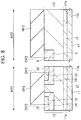
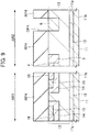
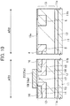
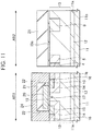
- Figs. 5 to 11 are fragmentary cross-sectional views showing the manufacturing process of the semiconductor device according to the first embodiment.
- AR1 shows the manufacturing process in the active region
- AR2 shows the manufacturing process in the end portion of the semiconductor device (hereinafter referred to as the chip end portion) .
- the method prepares the n + -type SiC substrate 11 (step S11 in Fig. 4 ).
- the method prepares the n + -type SiC substrate 11 including silicon carbide (SiC) in which an n-type impurity such as nitrogen (N) or phosphorus (P) is introduced.
- the n-type impurity concentration in the n + -type SiC substrate 11 is relatively high, for example, about 1 ⁇ 10 18 to 1 ⁇ 10 21 cm -3 .
- the thickness of the n + -type SiC substrate 11 is, for example, about 50 to 500 ⁇ m.
- the n + -type SiC substrate 11 is a thin sheet of silicon carbide (SiC) with a substantially circular shape in a plan view, which is called semiconductor wafer.
- the semiconductor device 1 is formed in each of a plurality of chip regions surrounded by a plurality of first scribe regions separated from each other in a first direction and extending in a second direction perpendicular to the first direction, and by a plurality of second scribe regions separated from each other in the second direction and extending in the first direction.
- the method forms the n-type buffer layer 12 (step S12 in Fig. 4 ).
- the method forms the buffer layer 12 by an epitaxial growth method on an upper surface 11a of the n + -type SiC substrate 11 both in the active region AR1 and the chip end portion AR2.
- the method forms the n-type buffer layer 12 including silicon carbide (SiC), for example, by using a process gas such as silicon (Si) atom-containing gas (SiH 4 gas), chlorine (Cl) atom-containing gas (HCl gas), carbon (C) atom-containing gas (C 3 H 8 gas), or reducing gas (H 2 gas) with a substrate temperature of, for example, about 1500 to 1800 °C.
- a process gas such as silicon (Si) atom-containing gas (SiH 4 gas), chlorine (Cl) atom-containing gas (HCl gas), carbon (C) atom-containing gas (C 3 H 8 gas), or reducing gas (H 2 gas) with a substrate temperature of, for example, about
- n-type impurity such as, for example, nitrogen (N) or phosphorus (P) is introduced in the n-type buffer layer 12.
- the n-type impurity concentration in the n-type buffer layer 12 is, for example, about 1 ⁇ 10 17 to 1 ⁇ 10 19 cm -3 , and the thickness of the n-type buffer layer 12 is, for example, about 3 to 20 ⁇ m.
- the method forms the n - -type epitaxial layer 13 (step S13 in Fig. 4 ).
- the method forms the n - -type epitaxial layer 13 by the epitaxial growth method on the upper surface of the n-type buffer layer 12 both in the active region AR1 and the chip end portion AR2.
- the method forms the n - -type epitaxial layer 13 including silicon carbide (SiC), for example, by using a process gas such as silicon (Si) atom-containing gas (SiH 4 gas), chlorine (Cl) atom-containing gas (HCl gas), carbon (C) atom-containing gas (C 3 H 8 gas), or reducing gas (H 2 gas) with a substrate temperature of, for example, about 1500 to 1800 °C.
- a process gas such as silicon (Si) atom-containing gas (SiH 4 gas), chlorine (Cl) atom-containing gas (HCl gas), carbon (C) atom-containing gas (C 3 H 8 gas), or reducing gas (H 2 gas) with a substrate temperature of, for example, about 1500 to 1800 °C.
- n-type impurity such as, for example, nitrogen (N) or phosphorus (P) is introduced in the n - -type epitaxial layer 13.
- the n-type impurity concentration in the n - -type epitaxial layer 13 is, for example, about 1 ⁇ 10 14 to 1 ⁇ 10 16 cm -3
- the thickness of the n - -type epitaxial layer 13 is, for example, about 5 to 50 ⁇ m.
- the method forms the p-type body region 14 and the p-type termination region 5 in each of the chip regions (step S14 in Fig. 4 ).
- the method forms a resist pattern RP1 by forming a resist film on the upper surface of the n - -type epitaxial layer 13 both in the active region AR1 and the chip end portion AR2, and by performing exposure and development processes on the formed resist film by using a photolithography technique.
- the resist pattern RP1 has an opening OP1 reaching the n - -type epitaxial layer 13 in an area of the active region AR1 in which the p-type body region 14 is formed, and also has an opening OP1 reaching the n - -type epitaxial layer 13 in an area of the chip end portion AR2 in which the p-type termination region 5 is formed.
- the method introduces a p-type impurity such as, for example, aluminum (Al) or boron (B), into the n - -type epitaxial layer 13 of the active region AR1 and the chip end portion AR2 by the ion implantation method with the resist pattern RP1 as a mask.
- a p-type impurity such as, for example, aluminum (Al) or boron (B)
- Al aluminum
- B boron
- the p-type impurity concentration in the p-type body region 14 and the p-type termination region 5 is, for example, about 1 ⁇ 10 17 to 1 ⁇ 10 18 cm -3
- the depth of the p-type body region 14 and the p-type termination region 5 from the upper surface of the n - -type epitaxial layer 13 is, for example, about 0.5 to 2 ⁇ m.
- the p-type impurity concentration in the p-type termination region 5 is preferably lower than the p-type impurity concentration of the p-type body region 14. In this way, it is possible to prevent or suppress the possibility that the intensity of the electric field in the vicinity of the p-type termination region 5 in the chip end portion AR2 will be greater than the intensity of the electric field in the vicinity of the p-type body region 14 in the active region AR1. Thus, the breakdown voltage of the semiconductor device can be increased.
- the p-type impurity concentration in the portion of the p-type termination region 5 on the opposite side of the active region AR1 is preferably lower than the p-type impurity concentration in the portion of the p-type termination region 5 on the side of the active region AR1. In this way, it is possible to prevent or suppress the possibility that the intensity of the electric field in the portion of the p-type termination region 5 on the opposite side of the active region AR1 will be greater than the intensity of the electric field in the portion of the p-type termination region 5 on the side of the active region AR1, so that the breakdown voltage of the semiconductor device can be increased. In this case, for example, the formation of the p-type body region 14 and the formation of the p-type termination region 5 should be performed in different steps.
- the implanted impurities are activated by performing a heat treatment at about 1700 °C.
- the method forms the n + -type source region 15 in each of the chip regions (step S15 in Fig. 4 ).
- the method forms a resist pattern RP2 by forming a resist film on the upper surface of the n - -type epitaxial layer 13 both in the active region AR1 and the chip end portion AR2, and by performing exposure and development processes on the formed resist film by using the photolithography technique.
- the resist pattern RP2 has an opening OP2 reaching the p-type body region 14 in an area of the active region AR1 in which the n + -type source region 15 is formed.
- the method introduces an n-type impurity such as, for example, nitrogen (N) phosphorus (P) into the p-type body region 14 of the active region AR1 by the ion implantation method with the resist pattern RP2 as a mask.
- an n-type impurity such as, for example, nitrogen (N) phosphorus (P) into the p-type body region 14 of the active region AR1 by the ion implantation method with the resist pattern RP2 as a mask.
- N nitrogen
- P phosphorus
- the n-type impurity concentration in the n + -type source region 15 is, for example, about 1 ⁇ 10 19 to 1 ⁇ 10 20 cm -3 , and the depth of the n + -type source region 15 from the upper surface of the n - -type epitaxial layer 13 is, for example, about 0.05 to 0.5 ⁇ m. Then, the resist pattern RP2 is removed.
- the method forms the p + -type potential fixing region 16 and the p + -type semiconductor region 4 in each of the chip regions (step S16 in Fig. 4 ).
- the method forms a resist pattern RP3 by forming a resist film on the upper surface of the n - -type epitaxial layer 13 both in the active region AR1 and the chip end portion AR2, and by performing exposure and development processes on the formed resist film by using the photolithography technique.
- the resist pattern RP3 has an opening OP3 reaching the n + -type source region 15 in an area of the active region AR1 in which the p + -type potential fixing region 16 is formed.
- the resist pattern RP3 has an opening OP3 reaching the n - -type epitaxial layer 13 in an area of the chip end portion AR2 in which the p + -type semiconductor region 4 is formed.
- the method introduces a p-type impurity such as, for example, aluminum (Al) or boron (B), into the n + -type source region 15 of the active region AR1 as well as the n - -type epitaxial layer 13 of the chip end portion AR2, by the ion implantation method with the resist pattern RP3 as a mask.
- a p-type impurity such as, for example, aluminum (Al) or boron (B)
- the p + -type potential fixing region 16 having a predetermined depth from the upper surface of the n - -type epitaxial layer 13 is formed within the n + -type source region 15, and the p + -type semiconductor region 4 having a predetermined depth from the upper surface of the n - -type epitaxial layer 13 is formed in the n - -type epitaxial layer 13 in the chip end portion AR2.
- the p-type impurity concentration in the p + -type potential fixing region 16 and the p + -type semiconductor region 4 is, for example, about 1 ⁇ 10 19 to 1 ⁇ 10 20 cm -3 .
- the depth of the p + -type potential fixing region 16 and the p + -type semiconductor region 4 from the upper surface of n - -type epitaxial layer 13 is, for example, about 0.05 to 0.5 ⁇ m. Then, the resist pattern RP3 is removed.
- the method forms the n-type hole annihilation region 6 in each of the chip regions (step S17 in Fig. 7 ).
- the method forms a resist pattern RP4 by forming a resist film on the upper surface of the n - -type epitaxial layer 13, and by performing exposure and development processes on the formed resist film by using the photolithography technique.
- the resist pattern RP4 has an opening OP4 reaching the n - -type epitaxial layer 13, in an area of the chip end portion AR2 in which the n-type hole annihilation region 6 is formed.
- the method introduces an n-type impurity such as, for example, nitrogen (N), phosphorus (P), or arsenic (As), into the n - -type epitaxial layer 13 of the chip end portion AR2, by the ion implantation method with the resist pattern RP4 as a mask.
- an n-type impurity such as, for example, nitrogen (N), phosphorus (P), or arsenic (As)
- N nitrogen
- P phosphorus
- As arsenic
- the n-type hole annihilation region 6 is formed with a predetermined depth from the upper surface of the n - -type epitaxial layer 13 in the chip end portion AR2.
- the p-type impurity concentration in the n-type hole annihilation region 6 is, for example, about 1 ⁇ 10 15 to 1 ⁇ 10 22 cm -3 .
- the depth of the n-type hole annihilation region 6 from the upper surface of the n - -type epitaxial layer 13 is, for example, about 0.5 ⁇ m.
- the hole annihilation region is configured with the n-type hole annihilation region 6 which is formed by introducing the n-type impurity into the n - -type epitaxial layer 13.
- the present invention is not limited to this configuration.
- the impurity concentration of the inert element is, for example, about 1 ⁇ 10 15 to 1 ⁇ 10 22 cm -3 .
- the order of the steps of forming the n + -type source region 15, p + -type potential fixing region 16, the p + -type semiconductor region 4, and the n-type hole annihilation region 6 is not limited to the order described above. These steps may be performed in any order as long as appropriately patterned suitably patterned resist films are used as masks in the steps. Further, it is also possible to use mask patterns including various films, instead of using the resist patterns including resist films.
- the implanted impurities are activated by performing a heat treatment at about 1700 °C.
- the method forms the gate insulating film 19 and the gate electrode 20 in each of the chip regions (step S18 in Fig. 4 ).
- the method forms an insulating film 19a on the upper surface of the n - -type epitaxial layer 13.
- various films including inorganic compounds such as, for example, silicon oxide (SiO 2 ), silicon oxynitride (SiON), aluminum oxide (Al 2 O 3 ), or hafnium oxide (HfO 2 ) can be used as the insulating film 19a.
- a laminated film in which the various films described above are laminated can preferably be used as the insulating film 19a.
- the insulating film 19a can be formed by, for example, a CVD (Chemical Vapor Deposition) method.
- the method forms a conductive film 20a on the insulating film 19a.
- a conductive film 20a for example, a conductive film including polysilicon in which an n-type impurity such as phosphorus (P) or arsenic (As) is diffused at a high concentration can be used, or a conductive film including polysilicon in which a p-type impurity such as boron (B) is diffused at a high concentration can be used.
- the conductive film 20a can be formed by, for example, the CVD method.
- the method forms the gate electrode 20 and the gate insulating film 19 by patterning the conductive film 20a and the insulating film 19a by photolithography and dry etching techniques.
- the gate insulating film 19 is continuously formed over from the upper surface of a certain p-type body region 14 to the upper surface of the p-type body region 14 adjacent to the former p-type body region 14, including the JFET region 17 sandwiched between the two p-type body regions 14. Further, in the example shown in Fig.
- the gate electrode 20 is continuously formed over from the upper surface of a certain p-type body region 14 to the p-type body region 14 adjacent to the former p-type body region 14, via the upper surface of the JFET region 17, with the gate insulating film 19 between these surfaces and the gate electrode 20.
- the method forms the interlayer insulating film 21 in each of the chip regions (step S19 in Fig. 4 ). At this time, the method forms the interlayer insulating film 21 over the n - -type epitaxial layer 13 so as to cover the gate electrode 20 and the gate insulating film 19.
- a film including silicon oxide (SiO 2 ), or the like can be used as the interlayer insulating film 21.
- the interlayer insulating film 21 can be formed by, for example, the CVD method.
- the method forms the source wiring electrode 24 in each of the chip regions (step S20 in Fig. 4 ).
- the method forms an opening 22 in the active region AR1, passing through the interlayer insulating film 21 to reach the n + -type source region 15 and the p + -type potential fixing region 16 by using the photolithography and etching techniques. Part of the upper surface of the n + -type source region 15 and the upper surface of the p + -type potential fixing region 16 are exposed on the bottom of the opening 22.
- the method forms the source wiring electrode 24 by depositing a conductive film including titanium (Ti), aluminum (Al), or the like, on the upper surface of the interlayer insulating film 21 including the interior of the opening 22 by using a vapor deposition or sputtering method, and then by patterning the conductive film by using photolithography and etching techniques. Note that, although not shown, a drain wiring electrode that is electrically connected to the gate electrode 20 is also formed at the formation of the source wiring electrode 24.
- the method forms the drain wiring electrode 26 in each of the chip regions (step S21 in Fig. 4 ).
- the method deposits a metal film including any one of titanium (Ti), nickel (Ni), gold (Au), and silver (Ag), or a laminated film in which two or more of the metal films are laminated, on a lower surface 11b of the n + -type SiC substrate 11 in the active region AR1 and the end portion AR2 by the deposition or sputtering method.
- the drain wiring electrode 26 can be formed on the lower surface 11b of the n + -type SiC substrate 11 in the active region AR1 and the termination region AR2.
- the semiconductor device 1 can be manufactured in each of the chip regions as shown in Figs. 2 and 3 .
- a passivation film can be formed on the upper surface of the semiconductor device 1 so as to cover the source wiring electrode 24 and the gate wiring electrode.
- an opening can be formed in a portion of the passivation film in which a pad region is formed to electrically connect the gate wiring electrode and the source wiring electrode 24 to the outside.
- the method cuts the wafer, in which a plurality of semiconductor devices 1 are formed, along the first scribe region and the second scribe region that are provided on the four sides of each of the chips by dicing to separate into individual semiconductor devices 1.
- the holes supplied from the p-type termination region 5 do not reach the dicing surface 7, so that it is possible to suppress the recombination of holes and electrons in the defects occurred in the dicing surface 7.
- energization deterioration is not likely to occur even if the return current flows through the body diode DI, so that it is possible to prevent the electrical resistance, or the on-resistance from increasing when the on current flows through the semiconductor device 1.
- the power module and the power converter can be miniaturized.
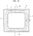
- FIG. 12 is a fragmentary plan view showing an example of a semiconductor device (semiconductor chip) according to the variation of the first embodiment.
- Fig. 13 is a fragmentary cross-sectional view (cross-sectional view taken along line C-C shown in Fig. 12 ) showing an enlarged part of the end portion of the semiconductor device (semiconductor chip) according to the variation of the first embodiment.
- the difference between the semiconductor device according to the variation and the semiconductor device 1 described above is the shape of the n-type hole annihilation region, so that the n-type hole annihilation region will be described in detail here.
- the other configurations are substantially the same as the semiconductor device 1 described above and the description thereof will be omitted.
- a semiconductor device (one semiconductor chip) 1a is configured with an active region (element forming region, activation region) 2 through which current mainly flows, and a peripheral region 3 formed around the active region 2 in a plan view.
- a termination structure for example, p + -type semiconductor region 4 and p-type termination region (termination) 5, is formed in the peripheral region 3 in order to prevent concentration of electric field.
- the p-type termination region 5 is formed so as to surround the p + -type semiconductor region 4 in a plan view.
- the p-type termination region 5 includes, for example, a junction termination extension (JTE) structure having a single- or multi-stage concentration distribution.
- JTE junction termination extension
- an n-type hole annihilation region 6a is formed apart from the p-type termination region 5.
- the n-type hole annihilation region 6a also has a function as a channel stopper.
- Fig. 13 shows an example of the arrangement of the p-type termination region 5 and the n-type hole annihilation region 6a that are formed in the end portion of the semiconductor device 1a.
- the n-type hole annihilation region 6a is formed apart from the p-type termination region 5 on the periphery of the p-type termination region 5 in a plan view.
- the n-type hole annihilation region 6 is apart from the dicing surface 7 of the semiconductor device 1.
- the n-type hole annihilation region 6a is formed also over the dicing surface 7 of the semiconductor device 1.
- the width (L NR ) of the n-type hole annihilation region 6a in a plan view is equal to
- the distance between the p-type termination region 5 and the n-type hole annihilation region 6a is set according to the breakdown voltage of the semiconductor device 1a, in such a way that the depletion layer end extending from the p-type termination region 5 at the time of non-energization (off state) will not reach the n-type hole annihilation region 6 and punch-through will not occur.
- the n-type hole annihilation region 6a has a predetermined depth (d NR ) from the upper surface of the n - -type epitaxial layer 13.
- the depth (d NR ) is equal to or more than the depth (d TM ) of the p-type termination region 5, which is located at a position closest to the n-type hole annihilation region 6a and facing the n-type hole annihilation region 6a, from the upper surface of the n - -type epitaxial layer 13.
- the depth (d NR ) of the n-type hole annihilation region 6a is, for example, about 0.5 ⁇ m.
- the n-type hole annihilation region 6a is provided in such a way that the sum of the width (L NR ) of the n-type hole annihilation region 6a in a plan view and the depth (d NR ) of the n-type hole annihilation region 6a is equal to or more than the thickness (d Epi ) of the n - -type epitaxial layer 13.
- the positon of the n-type hole annihilation region 6a is set by taking into account the diffusion of holes in the direction of the dicing surface 7 of the semiconductor substrate 1a.
- the n-type annihilation region 6a is provided in such a way that the sum of the width (L NR ) of the n-type hole annihilation region 6a and the depth (d NR ) of the n-type hole annihilation region 6a is equal to or more than the thickness (d Epi ) of the n - -type epitaxial layer 13.
- the semiconductor device 1a according to the first variation when the n-type hole annihilation region 6a is formed, the upper part of the dicing region is converted to amorphous by introducing an n-type impurity also in the dicing region by using the ion implantation method. In this way, it is possible to suppress the defects that occur in the dicing surface 7 of the semiconductor device 1a during dicing.
- the power module according to the second embodiment includes the semiconductor device according to the first embodiment described above. Note that the power module according to the second embodiment is configured such that the semiconductor device 1 is applied to a three-phase inverter.
- Fig. 14 is a diagram showing the configuration of a three-phase motor system according to the second embodiment.
- a three-phase motor system 30 includes a power converter 31 as an inverter device, a load 32 including a three-phase motor or the like, a DC power supply 33, and a capacitance 34 including a capacitor or the like.
- the power converter 31 includes a power module 35 as a three-phase inverter circuit, and a control circuit 36.
- the load 32 is connected to output terminals TO1, TO2, and TO3, which are three-phase output terminals of the power module 35.
- the DC power supply 33 and the capacitance 34 are connected in parallel to each other between two input terminals of the power module 35, input terminal TI1 and input terminal TI2.
- the power module 35 as a three-phase inverter circuit has switching elements 37u, 37v, 37w, 37x, 37y, and 37z.
- the switching elements 37u and 37x are connected in series between the input terminal TI1 and the input terminal TI2.
- the switching elements 37v and 37y are connected in series between the input terminal TI1 and the input terminal TI2.
- the switching elements 37w and 37z are connected in series between the input terminal TI1 and the input terminal TI2.
- Each of the switching elements 37u, 37v, 37w, 37x, 37y, and 37z includes a MOSFET 38 and a body diode 39.
- the semiconductor device 1 according to the first embodiment can be used as each of the switching elements 37u, 37v, 37w, 37x, 37y, and 37z.
- the body diode DI incorporated into the semiconductor device 1 can be used as the body diode 39.
- Gate electrodes of a plurality of MOSFETs 38 which are provided in the respective switching elements 37u, 37v, 37w, 37x, 37y, and 37z, are respectively connected to control terminals TC1, TC2, TC3, TC4, TC5, and TC6 which are six control terminals of the power module 35. Further, the control circuit 36 is connected to each of the control terminals TC1, TC2, TC3, TC4, TC5, and TC6. Thus, the control circuit 36 is connected to each of the gate electrodes of the MOSFETs 38 provided in the respective switching elements 37u, 37v, 37w, 37x, 37y, and 37z. The control circuit 36 drives the switching elements 37u, 37v, 37w, 37x, 37y, and 37z.
- the control circuit 36 drives each of the switching elements 37u, 37v, 37w, 37x, 37y, and 37z in such a way that the on and off states of each of the switching elements 37u, 37v, 37w, 37x, 37y, and 37z are alternately switched at a predetermined timing. In this way, AC voltages three phases of U phase, V phase, and W phase are generated to convert DC power to AC power of three phases.
- the load 32 is driven by the three-phase AC power.
- the semiconductor device 1 according to the first embodiment can be used as each of the switching elements 37u, 37v, 37w, 37x, 37y, and 37z in the power module 35 included in the power converter 31 according to the second embodiment.
- the automobile according to the third embodiment is an automobile including the power converter according to the second embodiment, such as a hybrid or electric vehicle.
- Fig. 15 is a diagram showing the configuration of an electric vehicle as the automobile according to the third embodiment.
- Fig. 16 is a circuit diagram showing a boost converter in the automobile according to the third embodiment.
- an automobile 40 as an electric vehicle, includes: a three-phase motor 43 capable of inputting and outputting power to a drive shaft 42 to which drive wheels 41a and 41b are connected; an inverter device 44 for driving the three-phase motor 43; and a battery 45. Further, the automobile 40 also includes a boost converter device 48, a relay 49, and an electronic control unit 50. The boost converter device 48 is connected to the inverter device 44 to which a power line 46 is connected, and to the power line 47 to which the battery 45 is connected.
- the three-phase motor 43 is a synchronous motor including a rotor in which a permanent magnet is embedded, and a stator around which a three-phase coil is wound.
- the power converter 31 (see Fig. 14 ) described in the second embodiment can be used as the inverter device 44.
- the boost converter device 48 is configured such that a reactor 51 and a smoothing capacitor 52 are connected to the inverter device 53.
- the inverter device 53 is similar to part of the inverter circuit included in the power module 35 described above in the second embodiment.
- a MOSFET 55 and a body diode 56 included in the switching element 54 in the inverter device 53 are similar to the MOSFET 38 and the body diode 39, respectively, described above in the second embodiment.
- the electronic control unit 50 includes a microprocessor, a storage device, and an input/output port.
- the electronic control unit 50 receives a signal from a sensor that detects the rotor position of the three-phase motor 43 or charge and discharge values of the battery 45. Then, the electronic control unit 50 outputs a signal to control the inverter device 44, the boost converter device 48, and the relay 49.
- the power converter 31 (see Fig. 14 ) according to the second embodiment above can be used as the inverter device 44 of the automobile 40 according to the third embodiment.
- the semiconductor device 1 according to the first embodiment can be used as each of the switching elements 37u, 37v, 37w, 37x, 37y, and 37z that are included in the power converter 31.
- the semiconductor device 1 according to the first embodiment above can be used as the switching element 54 provided in the inverter device 53 within the boost converter device 48 of the automobile 40 according to the third embodiment.
- the power loss can be reduced in power conversion in the inverter device 44 and the boost converter device 48, so that there will be no need to provide a large cooling system.
- the cooling system due to miniaturization of the cooling system or other design features, it is possible to easily reduce the cost and size or weight of the inverter device 44 and the boost converter device 48.
- the volume of the drive system that occupies the automobile 40 as the electric vehicle can be reduced.
- the third embodiment has described an example of applying the automobile including the power converter 31 according to the second embodiment to an electric vehicle.
- the automobile including the power converter 31 according to the second embodiment it is also possible to similarly apply the automobile including the power converter 31 according to the second embodiment to a hybrid vehicle using an engine in combination with a motor.
- the hybrid vehicle to which the power converter 31 according to the second embodiment is applied also has the same effect as the electric vehicle to which the power converter 31 according to the second embodiment is applied.
- a railway vehicle according to a fourth embodiment will be described.
- a railway vehicle according to the fourth embodiment is a railway vehicle including the power converter according to the second embodiment described above.
- Fig. 17 is a diagram showing the configuration of a railway vehicle according to the fourth embodiment.
- a railway vehicle 60 includes a pantograph 61 as a current collector, a transformer 62, a power converter 63, a load 64 which is an AC motor, and a wheel 65.
- the power converter 63 has a converter device 66, a capacitance 67 which is, for example, a capacitor, and an inverter device 68.
- the converter device 66 has switching elements 69 and 70.
- the switching element 69 is provided on the upper arm side, namely, on the high voltage side.
- the switching element 70 is provided on the lower arm side, namely, on the low voltage side. Note that in Fig. 17 , the switching elements 69 and 70 are shown with respect to one of a plurality of phases.
- the inverter device 68 has switching element 71 and 72.
- the switching element 71 is provided on the upper arm side, namely, on the high voltage side.
- the switching element 72 is provided on the lower arm side, namely, on the low voltage side. Note that in Fig. 17 , the switching elements 71 and 72 are shown with respect to one of the three phases of U phase, V phase, and W phase.
- An end on the primary side of the transformer 62 is connected to an overhead wire 61a through the pantograph 61.
- the other end on the primary side of the transformer 62 is connected to a railway track 65a through the wheel 65.
- An end on the secondary side of the transformer 62 is connected to a terminal of the converter device 66 on the upper arm side on the opposite side of load 64.
- the other end on the secondary side of the transformer 62 is connected to a terminal of the converter device 66 on the lower arm side on the opposite side of the load 64.
- a terminal on the upper arm side of the converter device 66 on the side of the load 64 is connected to a terminal on the upper arm side of the inverter device 68 on the opposite side of the load 64. Further, a terminal on the lower arm side of the converter device 66 on the side of the load 64 is connected to a terminal on the lower arm side of the inverter device 68 on the opposite side of the load 64. Further, the capacitance 67 is connected between the terminal on the upper arm side of the inverter device 68 on the opposite side of the load 64 and the terminal on the lower arm side of the inverter device 68 on the opposite side of the load 64. Further, although not shown in Fig. 17 , the three terminals on the output side of the inverter device 68 are connected to the load 64, respectively as U-phase, V-phase, and W-phase.
- the power converter 31 (see Fig. 14 ) according to the second embodiment can used as the inverter device 68.
- the AC power that is collected by the pantograph 61 from the overhead wire 61a is transformed in voltage with the transformer 62 and is converted to a desired DC power by the converter device 66.
- the voltage of the DC power converted by the converter device 66 is smoothed by the capacitance 67.
- the DC power with the voltage smoothed by the capacitance 67 is converted to AC power by the inverter device 68.
- the AC power converted by the inverter device 68 is supplied to the load 64.
- the load 64 to which the AC power is supplied rotates and drives the wheel 65. Thus, the railway vehicle is accelerated.
- the power converter 31 (see Fig. 14 ) according to the second embodiment can be used as the inverter device 68 of the railway vehicle 60 according to the fourth embodiment.
- the semiconductor device 1 according to the first embodiment can be used as each of the switching elements 37u, 37v, 37w, 37x, 37y, and 37z.
- the railway vehicle 60 according to the fourth embodiment can reduce the power loss in power conversion in the inverter device 68, so that there will be no need to provide a large cooling system.
- the cooling system due to miniaturization of the cooling system or other design features, it is possible to easily reduce the cost and size or weight of the inverter device 68. In this way, it is possible to easily reduce the cost of the railway vehicle 60 including the inverter device 68, and to increase the energy efficiency in operating the train.
- the semiconductor device 1 according to the first embodiment as the switching elements 69 and 70 included in the converter device 66.
- the power loss in power conversion in the converter device 66 can be reduce, so that it is possible to easily reduce the cost and size or weight of the converter device 66.
Landscapes
- Engineering & Computer Science (AREA)
- Power Engineering (AREA)
- Transportation (AREA)
- Mechanical Engineering (AREA)
- Electrodes Of Semiconductors (AREA)
Abstract
Description
- The present invention relates to a semiconductor device and a method of manufacturing the same, a power converter, a three-phase motor system, an automobile, and a railway vehicle.
- As the background art of this technical field, there is Japanese Unexamined Patent Application Publication No.
2012-59870 tan 18° or more. - Patent Literature 1: Japanese Unexamined Patent Application Publication No.
2012-59870 - For example, as a switching element of power module that configures a power converter, SiC-MOSFET (Metal Oxide Semiconductor Field Effect Transistor) is being developed by using SiC (silicon carbide) with a breakdown field higher than Si (silicon). In general, a freewheeling diode is provided outside the SiC-MOSFET in order to suppress the leakage current in the backward operation by reducing the electric field on the interface (Schottky interface) between metal and semiconductor when a voltage is applied in the opposite direction.
- Meanwhile, in order to downsize the power module, it is desirable that a freewheeling diode is incorporated into a substrate in which SiC-MOSFET is formed. However, when the return current flows through the built-in freewheeling diode (hereinafter, referred to as the body diode), "energization deterioration" is likely to occur due to crystal defects of SiC. Energization deterioration is a phenomenon such as an increase in the on-resistance which is the resistance in the energization of the SiC-MOSFET. The greater the on-resistance, the greater the loss and the more heat is generated, which affects the life or performance of the power module.
- Crystal defects of SiC, which are mainly stacking faults and micro defects as the origin of the stacking faults, are present in a manufactured SiC wafer. However, a large number of stacking faults also occur starting from defects occurring in the dicing surface in dicing of the SiC wafer. The crystal defects present in the manufactured SiC wafer can be reduced by improving the SiC wafer itself as well as the epitaxial growth on the SiC wafer. However, it is very difficult to reduce the number of defects that occur in the dicing surface in dicing of the SiC wafer. For this reason, the influence of the stacking faults that occur starting from the defects on energization deterioration of the SiC-MOSFET is significant. Solution to Problem
- In order to solve the above problems, the semiconductor device according to the present invention includes: an n--type epitaxial layer formed on a main surface of an n+-type SiC substrate; a p-type termination region annularly formed in the n--type epitaxial layer outside an active region; and an n-type hole annihilation region annularly formed in the n- type epitaxial layer outside a p-type termination region, apart from the p type termination region. Further, the n-type hole annihilation region has a first end surface facing a p-type termination region as well as a second end surface on the opposite side of the first end surface. Then, when a depth of the n-type hole annihilation region is dTM, a depth of the p-type termination region is dNR, the thickness of the n--type epitaxial layer is dEpi, a distance from the first end surface of the n-type hole annihilation region to the second end surface thereof is LNR, and a distance from the first end surface of the n-type hole annihilation region to the periphery of the semiconductor device is |XNR|, these variables have the following relationship: dNR≥dTM, (|XNR|+dNR)≥dEpi, 0<LNR<|XNR|.
- According to the present invention, it is possible to suppress energization deterioration due to crystal defects in a semiconductor device including SiC-MOSFET.
- The problems, configurations, and effects other than those described above will become apparent from the following description of exemplary embodiments.
-
-
Fig. 1 is a fragmentary plan view showing an example of a semiconductor device (semiconductor chip) according to a first embodiment. -
Fig. 2 is a fragmentary cross-sectional view showing an example of SiC-MOSFET according to the first embodiment. -
Fig. 3 is a fragmentary cross-sectional view showing an enlarged part of the end portion of the semiconductor device (semiconductor chip) according to the first embodiment. -
Fig. 4 is a flow chart illustrating an example of a manufacturing process of the semiconductor device according to the first embodiment. -
Fig. 5 is a fragmentary cross-sectional view showing the manufacturing process of the semiconductor device according to the first embodiment. -
Fig. 6 is a fragmentary cross-sectional view showing the manufacturing process of the semiconductor device, continued fromFig. 5 . -
Fig. 7 is a fragmentary cross-sectional view showing the manufacturing process of the semiconductor device, continued fromFig. 6 . -
Fig. 8 is a fragmentary cross-sectional view showing the manufacturing process of the semiconductor device, continued fromFig. 7 . -
Fig. 9 is a fragmentary cross-sectional view showing the manufacturing process of the semiconductor device, continued fromFig. 8 . -
Fig. 10 is a fragmentary cross-sectional view showing the manufacturing process of the semiconductor device, continued fromFig. 9 . -
Fig. 11 is a fragmentary cross-sectional view showing the manufacturing process of the semiconductor device, continued fromFig. 10 . -
Fig. 12 is a fragmentary plan view showing an example of a semiconductor device (semiconductor chip) according to a variation of the first embodiment. -
Fig. 13 is a fragmentary cross-sectional view showing an enlarged part of the end portion of the semiconductor device (semiconductor chip) according to the variation of the first embodiment. -
Fig. 14 is a diagram showing the configuration of a three-phase motor system according to a second embodiment. -
Fig. 15 is a diagram showing the configuration of an electric vehicle as an automobile according to a third embodiment. -
Fig. 16 is a circuit diagram showing a boost converter device in the automobile according to the third embodiment. -
Fig. 17 is a diagram showing the configuration of a railway vehicle according to a fourth embodiment. - The following embodiments will be explained by dividing them into a plurality of sections or embodiments, if necessary for convenience. However, they are not irrelevant to each other unless expressly stated otherwise, and are involved in relationships in which one is a variation, detail, supplement of a part or whole of the others.
- Further, in the following embodiments, when referring to the number of elements (including the number of pieces, numerical value, amount, range, and the like), the number of elements is not limited to a specific number unless expressly stated otherwise and unless the number is clearly limited to a specific number in principle or other reasons. The number of elements can be greater or smaller than the specific number.
- Further, in the following embodiments, it goes without saying that the components (including element steps and the like) are not necessarily required, unless expressly stated otherwise and unless they are considered to be clearly required in principle or other reasons.
- In addition, when referring to "including A", "composed of A", "having A", and "including A", it goes without saying that the elements other than the specified one should not be excluded, unless expressly stated the fact that there is only the particular element, or other reasons. Also, in the following embodiment, when referring to the shape, the positional relationship, or other characteristics of the components and the like, elements that substantially approximate or similar to the shape or other characteristics are included unless expressly stated otherwise and unless they are clearly considered not to be so in principle.
- Further, in the drawings used in the following embodiments, hatching may be used even in a plan view, to make the figure easy to understand. Further, in principle, elements having the same functions are denoted by the same reference numerals in all the drawings for describing the embodiments below, and the repetitive description thereof will be omitted. Hereinafter, preferred embodiments of the present invention will be described in detail with reference to the accompanying drawings.
- A semiconductor device according to a first embodiment will be described with reference to
Figs. 1 to 3 .Fig. 1 is a fragmentary plan view showing an example of the semiconductor device (semiconductor chip) according to the first embodiment.Fig. 2 is a fragmentary cross-sectional view showing an example of SiC-MOSFET according to the first embodiment (which is a cross-sectional view taken along line A-A shown inFig. 1 ). The SiC-MOSFET is MOSFET of planar type DMOS (Double diffused Metal Oxide Semiconductor) structure.Fig. 3 is a fragmentary cross-sectional view showing an enlarged part of the end portion of the semiconductor device (semiconductor chip) according to the first embodiment (which is a cross-sectional view taken along line B-B shown inFig. 1 ). - As shown in
Fig. 1 , a semiconductor device (a semiconductor chip) 1 is configured with an active region (element formation region, activation region) 2 through which current mainly flows, and aperipheral region 3 formed around theactive region 2 in a plan view. - For example, a plurality of n-channel type SiC-MOSFETs are connected in parallel to the
active region 2. Further, in order to prevent concentration of electric fields, a termination structure of, for example, p+-type semiconductor region 4 and p-type termination region (termination) 5 is formed in theperipheral region 3. In other words, the p-type termination region 5 is formed so as to surround the p+-type semiconductor region 4. The p-type termination region 5 includes, for example, a junction termination extension (JTE) structure having a single- or multi-stage concentration distribution. - Further, an n-type
hole annihilation region 6 is formed apart from the p-type termination region 5 on the side of the outer periphery (peripheral portion, end portion) of thesemiconductor device 1 than theperipheral region 3. The n-typehole annihilation region 6 also has a function as a channel stopper. The outer periphery of thesemiconductor device 1 is a dicingsurface 7 that is formed in dicing for cutting a plurality of semiconductor chips from a semiconductor wafer. -
Fig. 2 shows an example of the structure of the SiC-MOSFET formed in theactive region 2. - An n-
type buffer layer 12 composed of SiC with an impurity concentration lower than the impurity concentration of an n+-type SiC substrate 11 is formed on a surface (first main surface) of the n+-type SiC substrate 11 composed of SiC. Then, an n--type epitaxial layer 13 composed of SiC with an impurity concentration lower than the impurity concentration of the n-type buffer layer 12 is formed on the upper surface of the n-type buffer layer 12. - In the first embodiment, the n-
type buffer layer 12 is formed by an epitaxial growth method similarly to the n--type epitaxial layer 13. However, the n-type buffer layer 12 can also be formed by an ion implantation method. The thickness of the n-type buffer layer 12 is, for example, about 3 to 20 µm, and the thickness of the n--type epitaxial layer 13 is, for example, about 5 to 50 µm. Note that the n-type buffer 12 is formed in the first embodiment, but it may also be possible to directly form the n--type epitaxial layer 13 on the surface of the n+-type SiC substrate 11, without forming the n-buffer layer 12. - A plurality of p-type body regions (well regions) 14 are formed apart from each other within the n--
type epitaxial layer 13, with a predetermined depth from the upper surface of the n--type epitaxial layer 13. The depth of the p-type body region 14 from the upper surface of the n--type epitaxial layer 13 is, for example, about 0.5 to 2 µm. - An n+-
type source region 15 is formed within the p-type body region 14, with a predetermined depth from the upper surface of the n--type epitaxial layer 13. The n+-type source region 15 is formed within the p-type body region 14, apart from the end surface of the p-type body region 14. The depth of the n+-type source region 15 from the upper surface of the n--type epitaxial layer 13 is, for example, about 0.05 to 0.5 µm. - Further, a p+-type
potential fixing region 16 for fixing the potential of the p-type body region 14 is formed within the p-type body region 14, with a predetermined depth from the upper surface of the n--type epitaxial layer 13. The depth of the p+-typepotential fixing region 16 from the upper surface of the n--type epitaxial layer 13 is, for example, about 0.05 to 0.5 µm. - The region sandwiched between adjacent p-
type body regions 14 is the portion that functions as a JFET (Junction Field Effect Transistor) region (doped region) 17. Further, the p-type body region 4, which is located between the end surface of the p-type body region 14 (the interface between theJFET region 17 and the p-type body region 14) and the end surface of the n+-type source region 15 (the interface between the p-type body region 14 and the n+-type source region 15), is the portion that functions as achannel region 18. - Of the n--
type epitaxial layer 13, the region in which the p-type body region 14 and theJFET region 17 are not formed is a region that functions as an n- drift layer for enhancing the breakdown voltage. Further, the n+-type SiC substrate 11 is a region that functions as a drain layer. - Further, as indicated by the arrow in
Fig. 2 , a built-in diode, namely, a body diode DI is formed which includes the p+-typepotential fixing region 16, the p-type body region 14, the n--type epitaxial layer 13, the n-type buffer layer 12, and the n+-type SiC substrate 11, between asource wiring electrode 24 and adrain wiring electrode 16. - Note that "-" and "+" are signs that indicate relative impurity concentrations with the conductivity type of n-type or p-type. For example, the impurity concentration of n-type impurity increases in the order from "n-", "n", "n+", and the impurity concentration of p-type impurity increases in the order from "p-", "p", "p+".
- The preferred impurity concentration range of the n+-
type SiC substrate 11 is, for example, about 1×10¹⁸ to 1×1021 cm-3, the preferred impurity concentration range of the n-type buffer layer 12 is, for example, about 1×10¹⁷ to 1×1019 cm-3, and the preferred impurity concentration range of the n--type epitaxial layer 13 is, for example, about 1×10¹⁴ to 1×1016 cm-3. Further, the preferred impurity concentration range of the p-type body region 14 is, for example, about 1×10¹⁷ to 1×1018 cm-3, the preferred impurity concentration range of the n+-type source region 15 is, for example, about 1×10¹⁹ to 1×1020 cm-3, the preferred impurity concentration range of the p+-typepotential fixing region 16 is, for example, about 1×10¹⁹ to 1×1020 cm-3, and the preferred impurity concentration range of theJFET region 17 is, for example, about 3×1016 cm-3. Further, the preferred impurity concentration range of the n-typehole annihilation region 6 shown inFig. 1 is, for example, about 1×10¹⁵ to 1×1022 cm-3, the preferred impurity concentration region of the p+-type semiconductor region 4 is, for example, about 1×10¹⁹ to 1×1020 cm-3, and the preferred impurity concentration region of the p-type termination region 5 is, for example, about 1×10¹⁷ to 1×1018 cm-3. - A
gate insulating film 19 is formed over thechannel region 18, and agate electrode 20 is formed over thegate insulating film 19. Thegate electrode 20 is formed in a band shape in a plan view. Then, the p-type body region 14 is formed betweenadjacent gate electrodes 20 that are spaced apart from each other. Note that the layout of the SiC-MOSFET is not limited to this. For example, it may be possible that thegate electrode 20 is formed in a lattice pattern in a plan view and then the p-type body region 14 is formed to be surrounded by thegate electrode 20. - The
gate insulating film 19 and thegate electrode 20 are covered by aninterlayer insulating film 21. Part of the n+-type source region 15 as well as the p+-typepotential fixing region 16 are exposed in the bottom of anopening 22 formed in theinterlayer insulating film 21. Note that a metal silicide layer may be formed on these surfaces. Further, part of the n+-type source region 15 as well as the p+-typepotential fixing region 16 are electrically connected to thesource wiring electrode 24. Further, although not shown, thegate electrode 20 is electrically connected to the gate wiring electrode. - The back surface (second main surface) of the n+-
type SiC substrate 11 is electrically connected to thedrain wiring electrode 26. Note that a metal silicide layer may be formed on the back surface of the n+-type SiC substrate 11. The source potential is applied from the outside to thesource wiring electrode 24, the drain potential is applied from the outside to thedrain wiring electrode 26, and the gate potential is applied from the outside to the gate wiring electrode. -
Fig. 3 shows an example of the arrangement of the p-type termination region 5 and the n-typehole annihilation region 6, both of which are formed in the end portion of thesemiconductor device 1. - The n-type
hole annihilation region 6 is formed apart from the p-type termination region 5 and also apart from the outer periphery of thesemiconductor device 1, around the p-type termination region 5 in a plan view. The outer periphery of thesemiconductor device 1 is the dicingsurface 7 that is formed in dicing process in which a plurality of semiconductor chips are cut out of a semiconductor wafer. In the first embodiment, the position of the dicingsurface 7 of thesemiconductor device 1 is referred to as X0, the position of the end surface of the n-typehole annihilation region 6 that faces the p-type termination region 5 is referred to as XNR, and the distance between the dicingsurface 7 of thesemiconductor device 1 and the end surface of the n-typehole annihilation region 6 that faces the p-type termination region 5 is referred to as |XNR|. - The n-type
hole annihilation region 6 has a predetermined width (LNR) in a plan view. The width (LNR) is set smaller than |XNR| which is the distance between the dicingsurface 7 of thesemiconductor device 1 and the end surface of the n-typehole annihilation region 6 that faces the p-type termination region 5. The width (LNR) of the n-typehole annihilation region 6 can be, for example, about 1 µm. Further, the distance between the p-type termination region 5 and the n-typehole annihilation region 6 is set according to the breakdown voltage of thesemiconductor device 1 in such a way that the depletion layer end extending from the p-type termination region 5 at the time of non-energization (off state) does not reaches the n-typehole annihilation region 6 and punch-through does not occur. - Further, the n-type
hole annihilation region 6 has a predetermined depth (dNR) from the upper surface of the n--type epitaxial layer 13. The depth (dNR) is equal to or more than the depth (dTM) of the p-type termination region 5, which is located at a position closest to the n-typehole annihilation region 6, from the upper surface of the n--type epitaxial layer 13. The depth (dNR) of the n-typehole annihilation region 6 can be, for example, about 0.5 µm. - Further, the n-type
hole annihilation region 6 is formed in such a way that the sum of the distance (|XNR|) from the dicingsurface 7 of thesemiconductor device 1 to the end surface of the n-typehole annihilation region 6 that faces the p-type termination region 5, and the depth (dNR) of the n-typehole annihilation region 6 is equal to or more than the thickness (dEpi) of the n--type epitaxial layer 13. - To summarize the above, the following equation is obtained:


- The effect obtained by forming the n-type
hole annihilation region 6 to satisfy the above equation will be described below with reference toFig. 3 . - A semiconductor wafer in which many semiconductor chips are formed is cut along scribe regions (also referred to as dicing regions or cutting margins) provided on the four sides of each of the semiconductor chips, and is separated into individual semiconductor chips. In the dicing process, a defect occurs in the dicing surface of the semiconductor chip, and a number of stacking faults occur within the SiC crystal starting from the defect occurring in the dicing surface.
- According to the study of the present inventors, it was found that when a hole was induced in the dicing surface, a number of stacking faults occurred within the SiC crystal starting from a defect occurring in the dicing surface.
- More specifically, the present inventors conducted an ultraviolet irradiation experiment on the semiconductor chip after dicing. In other words, the present inventors have studied the relationship between holes and defects that occur in the dicing surface, by taking advantage of the phenomenon that when holes induced by ultraviolet light within the SiC crystal recombine with electrons in stacking faults or in micro defects which are the origin of the stacking faults, these defects are extended and the incident light intensity is increased. Ultraviolet light was emitted obliquely from above the semiconductor chip. As a result, it was found that although the incident light intensity at the dicing surface of the semiconductor chip was dependent on the emission direction of the ultraviolet light, the incident light intensity at the surface other than the dicing surface of the semiconductor chip was independent of the irradiation direction of the ultraviolet light. From this fact, it was believed that the stacking faults, which grow depending on the emission direction of the ultraviolet light, occurred from the dicing surface.
- Thus, in the first embodiment, as shown in
Fig. 3 , the n-typehole annihilation region 6 was provided between the p-type termination region 5 and thedicing surface 7 of thesemiconductor device 1 in such a way that the holes supplied in the energization did not reach thedicing surface 7 of thesemiconductor device 1. - In other words, when holes and electrons are recombined in the defects occurred in the
dicing surface 7 of thesemiconductor device 1, the defects are further extended by the energy emitted by the recombination of holes and electrons, and as a result, a number of stacking faults occur in the n--type epitaxial layer 13. However, according to the first embodiment, because the n-typehole annihilation region 6 is provided, the holes are recombined and disappear in the n-typehole annihilation region 6 and do not reach thedicing surface 7 of thesemiconductor device 1, so that it is possible to suppress the recombination of holes and electrons in the defects occurred in thedicing surface 7 of thesemiconductor device 1. As a result, it is possible to prevent the occurrence of stacking faults in the n--type epitaxial layer 13, or the like, starting from the defects occurred in thedicing surface 7 of thesemiconductor device 1. - For example, in the energization, when a positive voltage is applied to the p-
type termination region 5 and a voltage of 0 V is applied to the n-type buffer layer 12, many of the holes supplied from the p-type termination region 5 diffuse to the n-type buffer layer 12, but at the same time, some of the holes diffuse in the direction of the dicingsurface 7 of thesemiconductor substrate 1. However, some holes diffusing in the dicing direction of thesemiconductor substrate 1 are recombined and disappear in the n-typehole annihilation region 6 and do not reach thedicing surface 7 of thesemiconductor device 1. As a result, it is possible to suppress the occurrence of stacking faults starting from the defects occurred in thedicing surface 7 of thesemiconductor device 1. In this way, energization deterioration is unlikely to occur even if the return current flows through the body diode DI, so that it is possible to prevent an increase in the electrical resistance, namely, the on-resistance when the on current flows through thesemiconductor device 1. - Further, in the first embodiment, energization deterioration is unlikely to occur even if the return current flows through the body diode DI incorporated into the
semiconductor device 1, so that there is no need to provide an external diode separately from the body diode DI incorporated into thesemiconductor device 1. As a result, the power module and the power converter can be miniaturized. - Meanwhile, as described above, some holes also diffuse in the direction of the dicing
surface 7 of thesemiconductor device 1. Thus, even if the n-typehole annihilation region 6 is provided as shown inFig. 3 , there is a possibility that the holes will reach thedicing surface 7 of thesemiconductor device 1 if the end surface of the n-typehole annihilation region 6 that faces the p-type termination region 5 is close to thedicing surface 7. - For example, the paragraphs [0046] to [0050] of
Patent Literature 1 as well asFig. 7 describe the fact that the concentration of the holes diffusing in the range of 18 degrees in the normal direction of the lower surface of a p+-type propagation region is particularly high, and that the concentration of the holes diffusing in the range of 22 degrees is increased. Further as described, for example, in the paragraph [0093] of Japanese Unexamined Patent Application Publication No.2009-392510 - Thus, in the first embodiment, the position of the n-type
hole annihilation region 6 is set by taking into account the diffusion of holes in the direction of the dicingsurface 7 of thesemiconductor substrate 1. In other words, as described above, the n-typehole annihilation region 6 is provided in such a way that the sum of the distance (|XNR|) between the dicingsurface 7 of thesemiconductor device 1 and the end surface of the n-typehole annihilation region 6 that faces the p-type termination region 5, and the depth (dNR) of the n-typehole annihilation region 6 is equal to or more than the thickness (dEpi) of the n--type epitaxial layer 13. - Next, an example of a manufacturing method of the semiconductor device according to the first embodiment will be described with reference to
Figs. 4 to 11 .Fig. 4 is a flow chart illustrating an example of a manufacturing process of the semiconductor device according to the first embodiment.Figs. 5 to 11 are fragmentary cross-sectional views showing the manufacturing process of the semiconductor device according to the first embodiment. InFigs. 5 to 11 , AR1 shows the manufacturing process in the active region, while AR2 shows the manufacturing process in the end portion of the semiconductor device (hereinafter referred to as the chip end portion) . - First, as shown in
Fig. 5 , the method prepares the n+-type SiC substrate 11 (step S11 inFig. 4 ). For example, the method prepares the n+-type SiC substrate 11 including silicon carbide (SiC) in which an n-type impurity such as nitrogen (N) or phosphorus (P) is introduced. The n-type impurity concentration in the n+-type SiC substrate 11 is relatively high, for example, about 1×10¹⁸ to 1×1021 cm-3. Further, the thickness of the n+-type SiC substrate 11 is, for example, about 50 to 500 µm. Note that in this stage, the n+-type SiC substrate 11 is a thin sheet of silicon carbide (SiC) with a substantially circular shape in a plan view, which is called semiconductor wafer. Thesemiconductor device 1 is formed in each of a plurality of chip regions surrounded by a plurality of first scribe regions separated from each other in a first direction and extending in a second direction perpendicular to the first direction, and by a plurality of second scribe regions separated from each other in the second direction and extending in the first direction. - Next, the method forms the n-type buffer layer 12 (step S12 in
Fig. 4 ). The method forms thebuffer layer 12 by an epitaxial growth method on anupper surface 11a of the n+-type SiC substrate 11 both in the active region AR1 and the chip end portion AR2. At this time, the method forms the n-type buffer layer 12 including silicon carbide (SiC), for example, by using a process gas such as silicon (Si) atom-containing gas (SiH4 gas), chlorine (Cl) atom-containing gas (HCl gas), carbon (C) atom-containing gas (C3H8 gas), or reducing gas (H2 gas) with a substrate temperature of, for example, about 1500 to 1800 °C. - An n-type impurity such as, for example, nitrogen (N) or phosphorus (P) is introduced in the n-
type buffer layer 12. The n-type impurity concentration in the n-type buffer layer 12 is, for example, about 1×10¹⁷ to 1×1019 cm-3, and the thickness of the n-type buffer layer 12 is, for example, about 3 to 20 µm. - Next, the method forms the n--type epitaxial layer 13 (step S13 in
Fig. 4 ). The method forms the n--type epitaxial layer 13 by the epitaxial growth method on the upper surface of the n-type buffer layer 12 both in the active region AR1 and the chip end portion AR2. At this time, the method forms the n--type epitaxial layer 13 including silicon carbide (SiC), for example, by using a process gas such as silicon (Si) atom-containing gas (SiH4 gas), chlorine (Cl) atom-containing gas (HCl gas), carbon (C) atom-containing gas (C3H8 gas), or reducing gas (H2 gas) with a substrate temperature of, for example, about 1500 to 1800 °C. - An n-type impurity such as, for example, nitrogen (N) or phosphorus (P) is introduced in the n--
type epitaxial layer 13. The n-type impurity concentration in the n--type epitaxial layer 13 is, for example, about 1×10¹⁴ to 1×1016 cm-3, and the thickness of the n--type epitaxial layer 13 is, for example, about 5 to 50 µm. - Next, as shown in
Fig. 6 , the method forms the p-type body region 14 and the p-type termination region 5 in each of the chip regions (step S14 inFig. 4 ). The method forms a resist pattern RP1 by forming a resist film on the upper surface of the n--type epitaxial layer 13 both in the active region AR1 and the chip end portion AR2, and by performing exposure and development processes on the formed resist film by using a photolithography technique. The resist pattern RP1 has an opening OP1 reaching the n--type epitaxial layer 13 in an area of the active region AR1 in which the p-type body region 14 is formed, and also has an opening OP1 reaching the n--type epitaxial layer 13 in an area of the chip end portion AR2 in which the p-type termination region 5 is formed. - Next, the method introduces a p-type impurity such as, for example, aluminum (Al) or boron (B), into the n--
type epitaxial layer 13 of the active region AR1 and the chip end portion AR2 by the ion implantation method with the resist pattern RP1 as a mask. In this way, the p-type body region 14 having a predetermined depth from the upper surface of the n--type epitaxial layer 13 is formed in the active region AR1. Further, the p-type termination region 5 having a predetermined depth from the upper surface of the n--type epitaxial layer 13 is formed in the chip end portion AR2. The p-type impurity concentration in the p-type body region 14 and the p-type termination region 5 is, for example, about 1×10¹⁷ to 1×1018 cm-3, and the depth of the p-type body region 14 and the p-type termination region 5 from the upper surface of the n--type epitaxial layer 13 is, for example, about 0.5 to 2 µm. Then, the resist pattern RP1 is removed. - Note that the p-type impurity concentration in the p-
type termination region 5 is preferably lower than the p-type impurity concentration of the p-type body region 14. In this way, it is possible to prevent or suppress the possibility that the intensity of the electric field in the vicinity of the p-type termination region 5 in the chip end portion AR2 will be greater than the intensity of the electric field in the vicinity of the p-type body region 14 in the active region AR1. Thus, the breakdown voltage of the semiconductor device can be increased. - Further, the p-type impurity concentration in the portion of the p-
type termination region 5 on the opposite side of the active region AR1 is preferably lower than the p-type impurity concentration in the portion of the p-type termination region 5 on the side of the active region AR1. In this way, it is possible to prevent or suppress the possibility that the intensity of the electric field in the portion of the p-type termination region 5 on the opposite side of the active region AR1 will be greater than the intensity of the electric field in the portion of the p-type termination region 5 on the side of the active region AR1, so that the breakdown voltage of the semiconductor device can be increased. In this case, for example, the formation of the p-type body region 14 and the formation of the p-type termination region 5 should be performed in different steps. - Next, with respect to the step of forming the p-
type body region 14 and the p-type termination region 5, after this step is completed, the implanted impurities are activated by performing a heat treatment at about 1700 °C. - Next, as shown in
Fig. 7 , the method forms the n+-type source region 15 in each of the chip regions (step S15 inFig. 4 ). At this time, the method forms a resist pattern RP2 by forming a resist film on the upper surface of the n--type epitaxial layer 13 both in the active region AR1 and the chip end portion AR2, and by performing exposure and development processes on the formed resist film by using the photolithography technique. The resist pattern RP2 has an opening OP2 reaching the p-type body region 14 in an area of the active region AR1 in which the n+-type source region 15 is formed. - Next, the method introduces an n-type impurity such as, for example, nitrogen (N) phosphorus (P) into the p-
type body region 14 of the active region AR1 by the ion implantation method with the resist pattern RP2 as a mask. In this way, the n+-type source region 15 having a predetermined depth from the upper surface of the n--type epitaxial layer 13 is formed within the p-type body region 13. The n-type impurity concentration in the n+-type source region 15 is, for example, about 1×10¹⁹ to 1×1020 cm-3, and the depth of the n+-type source region 15 from the upper surface of the n--type epitaxial layer 13 is, for example, about 0.05 to 0.5 µm. Then, the resist pattern RP2 is removed. - Next, as shown in
Fig. 8 , the method forms the p+-typepotential fixing region 16 and the p+-type semiconductor region 4 in each of the chip regions (step S16 inFig. 4 ). At this time, the method forms a resist pattern RP3 by forming a resist film on the upper surface of the n--type epitaxial layer 13 both in the active region AR1 and the chip end portion AR2, and by performing exposure and development processes on the formed resist film by using the photolithography technique. The resist pattern RP3 has an opening OP3 reaching the n+-type source region 15 in an area of the active region AR1 in which the p+-typepotential fixing region 16 is formed. Also, the resist pattern RP3 has an opening OP3 reaching the n--type epitaxial layer 13 in an area of the chip end portion AR2 in which the p+-type semiconductor region 4 is formed. - Next, the method introduces a p-type impurity such as, for example, aluminum (Al) or boron (B), into the n+-
type source region 15 of the active region AR1 as well as the n--type epitaxial layer 13 of the chip end portion AR2, by the ion implantation method with the resist pattern RP3 as a mask. In this way, the p+-typepotential fixing region 16 having a predetermined depth from the upper surface of the n--type epitaxial layer 13 is formed within the n+-type source region 15, and the p+-type semiconductor region 4 having a predetermined depth from the upper surface of the n--type epitaxial layer 13 is formed in the n--type epitaxial layer 13 in the chip end portion AR2. The p-type impurity concentration in the p+-typepotential fixing region 16 and the p+-type semiconductor region 4 is, for example, about 1×10¹⁹ to 1×1020 cm-3. The depth of the p+-typepotential fixing region 16 and the p+-type semiconductor region 4 from the upper surface of n--type epitaxial layer 13 is, for example, about 0.05 to 0.5 µm. Then, the resist pattern RP3 is removed. - Next, as shown in
Fig. 9 , the method forms the n-typehole annihilation region 6 in each of the chip regions (step S17 inFig. 7 ). At this time, the method forms a resist pattern RP4 by forming a resist film on the upper surface of the n--type epitaxial layer 13, and by performing exposure and development processes on the formed resist film by using the photolithography technique. The resist pattern RP4 has an opening OP4 reaching the n--type epitaxial layer 13, in an area of the chip end portion AR2 in which the n-typehole annihilation region 6 is formed. - Next, the method introduces an n-type impurity such as, for example, nitrogen (N), phosphorus (P), or arsenic (As), into the n--
type epitaxial layer 13 of the chip end portion AR2, by the ion implantation method with the resist pattern RP4 as a mask. For example, in the case of thesemiconductor device 1 having a breakdown voltage of 3.3 keV, the following can be cited as an example of ion implantation conditions of n-type impurities: the energy is 400 keV and the dose amount is 1×1013 cm-2. In this way, the n-typehole annihilation region 6 is formed with a predetermined depth from the upper surface of the n--type epitaxial layer 13 in the chip end portion AR2. The p-type impurity concentration in the n-typehole annihilation region 6 is, for example, about 1×10¹⁵ to 1×1022 cm-3. The depth of the n-typehole annihilation region 6 from the upper surface of the n--type epitaxial layer 13 is, for example, about 0.5 µm. - Note that in the first embodiment, the hole annihilation region is configured with the n-type
hole annihilation region 6 which is formed by introducing the n-type impurity into the n--type epitaxial layer 13. However, the present invention is not limited to this configuration. For example, it may also be possible to form the hole annihilation region by introducing an inert element such as, for example, helium (He) or argon (Ar), into the n--type epitaxial layer 13. In this case also, the impurity concentration of the inert element is, for example, about 1×10¹⁵ to 1×1022 cm-3. - Further, the order of the steps of forming the n+-
type source region 15, p+-typepotential fixing region 16, the p+-type semiconductor region 4, and the n-typehole annihilation region 6 is not limited to the order described above. These steps may be performed in any order as long as appropriately patterned suitably patterned resist films are used as masks in the steps. Further, it is also possible to use mask patterns including various films, instead of using the resist patterns including resist films. - Next, with respect to the steps of forming the n+-
type source region 15, the p+-typepotential fixing region 16, the p+-type semiconductor region 4, and the n-typehole annihilation region 6, after each step or after all the steps are completed, the implanted impurities are activated by performing a heat treatment at about 1700 °C. - Next, as shown in
Fig. 10 , the method forms thegate insulating film 19 and thegate electrode 20 in each of the chip regions (step S18 inFig. 4 ). First, the method forms an insulatingfilm 19a on the upper surface of the n--type epitaxial layer 13. Preferably, various films including inorganic compounds, such as, for example, silicon oxide (SiO2), silicon oxynitride (SiON), aluminum oxide (Al2O3), or hafnium oxide (HfO2) can be used as the insulatingfilm 19a. Alternatively, a laminated film in which the various films described above are laminated can preferably be used as the insulatingfilm 19a. Further, the insulatingfilm 19a can be formed by, for example, a CVD (Chemical Vapor Deposition) method. - Next, the method forms a
conductive film 20a on the insulatingfilm 19a. As theconductive film 20a, for example, a conductive film including polysilicon in which an n-type impurity such as phosphorus (P) or arsenic (As) is diffused at a high concentration can be used, or a conductive film including polysilicon in which a p-type impurity such as boron (B) is diffused at a high concentration can be used. Further, theconductive film 20a can be formed by, for example, the CVD method. - Next, the method forms the
gate electrode 20 and thegate insulating film 19 by patterning theconductive film 20a and the insulatingfilm 19a by photolithography and dry etching techniques. In the example shown inFig. 10 , thegate insulating film 19 is continuously formed over from the upper surface of a certain p-type body region 14 to the upper surface of the p-type body region 14 adjacent to the former p-type body region 14, including theJFET region 17 sandwiched between the two p-type body regions 14. Further, in the example shown inFig. 10 , thegate electrode 20 is continuously formed over from the upper surface of a certain p-type body region 14 to the p-type body region 14 adjacent to the former p-type body region 14, via the upper surface of theJFET region 17, with thegate insulating film 19 between these surfaces and thegate electrode 20. - Next, as shown in
Fig. 11 , the method forms theinterlayer insulating film 21 in each of the chip regions (step S19 inFig. 4 ). At this time, the method forms theinterlayer insulating film 21 over the n--type epitaxial layer 13 so as to cover thegate electrode 20 and thegate insulating film 19. For example, a film including silicon oxide (SiO2), or the like, can be used as theinterlayer insulating film 21. Theinterlayer insulating film 21 can be formed by, for example, the CVD method. - Next, the method forms the
source wiring electrode 24 in each of the chip regions (step S20 inFig. 4 ). First, the method forms anopening 22 in the active region AR1, passing through theinterlayer insulating film 21 to reach the n+-type source region 15 and the p+-typepotential fixing region 16 by using the photolithography and etching techniques. Part of the upper surface of the n+-type source region 15 and the upper surface of the p+-typepotential fixing region 16 are exposed on the bottom of theopening 22. - Next, the method forms the
source wiring electrode 24 by depositing a conductive film including titanium (Ti), aluminum (Al), or the like, on the upper surface of theinterlayer insulating film 21 including the interior of theopening 22 by using a vapor deposition or sputtering method, and then by patterning the conductive film by using photolithography and etching techniques. Note that, although not shown, a drain wiring electrode that is electrically connected to thegate electrode 20 is also formed at the formation of thesource wiring electrode 24. - Next, the method forms the
drain wiring electrode 26 in each of the chip regions (step S21 inFig. 4 ). For example, the method deposits a metal film including any one of titanium (Ti), nickel (Ni), gold (Au), and silver (Ag), or a laminated film in which two or more of the metal films are laminated, on alower surface 11b of the n+-type SiC substrate 11 in the active region AR1 and the end portion AR2 by the deposition or sputtering method. In this way, thedrain wiring electrode 26 can be formed on thelower surface 11b of the n+-type SiC substrate 11 in the active region AR1 and the termination region AR2. Thus, thesemiconductor device 1 can be manufactured in each of the chip regions as shown inFigs. 2 and 3 . - Although not shown in
Figs. 2 and 3 , after the formation of thedrain wiring electrode 26, a passivation film can be formed on the upper surface of thesemiconductor device 1 so as to cover thesource wiring electrode 24 and the gate wiring electrode. Next, an opening can be formed in a portion of the passivation film in which a pad region is formed to electrically connect the gate wiring electrode and thesource wiring electrode 24 to the outside. - Then, the method cuts the wafer, in which a plurality of
semiconductor devices 1 are formed, along the first scribe region and the second scribe region that are provided on the four sides of each of the chips by dicing to separate intoindividual semiconductor devices 1. - In this way, according to the first embodiment, even if defects occur in the
dicing surface 7 of thesemiconductor device 1, the holes supplied from the p-type termination region 5 do not reach thedicing surface 7, so that it is possible to suppress the recombination of holes and electrons in the defects occurred in thedicing surface 7. Thus, it is possible to prevent that the defects occurred in thedicing surface 7 of thesemiconductor device 1 are extended and a number of stacking faults occur in the n--type epitaxial layer 13 or the like. Thus, energization deterioration is not likely to occur even if the return current flows through the body diode DI, so that it is possible to prevent the electrical resistance, or the on-resistance from increasing when the on current flows through thesemiconductor device 1. Further, because energization deterioration is not likely to occur even if the return current flows through the body diode ID incorporated into thesemiconductor device 1, there is no need to provide an external diode separately from the body diode DI incorporated into thesemiconductor device 1. Thus, the power module and the power converter can be miniaturized. - A semiconductor device according to a variation of the first embodiment will be described with reference to
Figs. 12 and13 .Fig. 12 is a fragmentary plan view showing an example of a semiconductor device (semiconductor chip) according to the variation of the first embodiment.Fig. 13 is a fragmentary cross-sectional view (cross-sectional view taken along line C-C shown inFig. 12 ) showing an enlarged part of the end portion of the semiconductor device (semiconductor chip) according to the variation of the first embodiment. Note that the difference between the semiconductor device according to the variation and thesemiconductor device 1 described above is the shape of the n-type hole annihilation region, so that the n-type hole annihilation region will be described in detail here. The other configurations are substantially the same as thesemiconductor device 1 described above and the description thereof will be omitted. - As shown in
Fig. 12 , similarly to thesemiconductor device 1 described above, a semiconductor device (one semiconductor chip) 1a is configured with an active region (element forming region, activation region) 2 through which current mainly flows, and aperipheral region 3 formed around theactive region 2 in a plan view. - For example, a plurality of n-channel type SiC-MOSFETs are connected in parallel to the
active region 2. Further, a termination structure, for example, p+-type semiconductor region 4 and p-type termination region (termination) 5, is formed in theperipheral region 3 in order to prevent concentration of electric field. In other words, the p-type termination region 5 is formed so as to surround the p+-type semiconductor region 4 in a plan view. The p-type termination region 5 includes, for example, a junction termination extension (JTE) structure having a single- or multi-stage concentration distribution. - Further, on the outer periphery (termination, end portion) of the
semiconductor device 1a than theperipheral region 3, an n-typehole annihilation region 6a is formed apart from the p-type termination region 5. The n-typehole annihilation region 6a also has a function as a channel stopper. -
Fig. 13 shows an example of the arrangement of the p-type termination region 5 and the n-typehole annihilation region 6a that are formed in the end portion of thesemiconductor device 1a. - The n-type
hole annihilation region 6a is formed apart from the p-type termination region 5 on the periphery of the p-type termination region 5 in a plan view. In thesemiconductor device 1 described above, the n-typehole annihilation region 6 is apart from the dicingsurface 7 of thesemiconductor device 1. However, in thesemiconductor device 1a according to the variation, the n-typehole annihilation region 6a is formed also over the dicingsurface 7 of thesemiconductor device 1. - Thus, the width (LNR) of the n-type
hole annihilation region 6a in a plan view is equal to |XNR| which is the distance between the dicingsurface 7 of thesemiconductor device 1a and the end surface of the n-type annihilation region 6a that faces the p-type termination region 5. The distance between the p-type termination region 5 and the n-typehole annihilation region 6a is set according to the breakdown voltage of thesemiconductor device 1a, in such a way that the depletion layer end extending from the p-type termination region 5 at the time of non-energization (off state) will not reach the n-typehole annihilation region 6 and punch-through will not occur. - Further, the n-type
hole annihilation region 6a has a predetermined depth (dNR) from the upper surface of the n--type epitaxial layer 13. The depth (dNR) is equal to or more than the depth (dTM) of the p-type termination region 5, which is located at a position closest to the n-typehole annihilation region 6a and facing the n-typehole annihilation region 6a, from the upper surface of the n--type epitaxial layer 13. The depth (dNR) of the n-typehole annihilation region 6a is, for example, about 0.5 µm. - Further, the n-type
hole annihilation region 6a is provided in such a way that the sum of the width (LNR) of the n-typehole annihilation region 6a in a plan view and the depth (dNR) of the n-typehole annihilation region 6a is equal to or more than the thickness (dEpi) of the n--type epitaxial layer 13. - To summarize the above, the following equation is obtained:
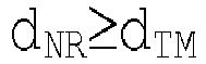

- It is possible to obtain substantially the same effect as the n-type
hole annihilation region 6 formed in thesemiconductor device 1 described above, by forming the n-typehole annihilation region 6a so as to satisfy the above equation. - Further, also in the
semiconductor device 1a according to the variation, the positon of the n-typehole annihilation region 6a is set by taking into account the diffusion of holes in the direction of the dicingsurface 7 of thesemiconductor substrate 1a. In other words, the n-type annihilation region 6a is provided in such a way that the sum of the width (LNR) of the n-typehole annihilation region 6a and the depth (dNR) of the n-typehole annihilation region 6a is equal to or more than the thickness (dEpi) of the n--type epitaxial layer 13. - Further, in the
semiconductor device 1a according to the first variation, when the n-typehole annihilation region 6a is formed, the upper part of the dicing region is converted to amorphous by introducing an n-type impurity also in the dicing region by using the ion implantation method. In this way, it is possible to suppress the defects that occur in thedicing surface 7 of thesemiconductor device 1a during dicing. - A power module, a power converter, and a three-phase motor system including the power converter according to a second embodiment will be described. The power module according to the second embodiment includes the semiconductor device according to the first embodiment described above. Note that the power module according to the second embodiment is configured such that the
semiconductor device 1 is applied to a three-phase inverter. -
Fig. 14 is a diagram showing the configuration of a three-phase motor system according to the second embodiment. - As shown in
Fig. 14 , a three-phase motor system 30 includes apower converter 31 as an inverter device, aload 32 including a three-phase motor or the like, aDC power supply 33, and acapacitance 34 including a capacitor or the like. Thepower converter 31 includes apower module 35 as a three-phase inverter circuit, and acontrol circuit 36. Theload 32 is connected to output terminals TO1, TO2, and TO3, which are three-phase output terminals of thepower module 35. Further, theDC power supply 33 and thecapacitance 34 are connected in parallel to each other between two input terminals of thepower module 35, input terminal TI1 and input terminal TI2. - The
power module 35 as a three-phase inverter circuit has switchingelements switching elements elements switching elements - Each of the
switching elements MOSFET 38 and abody diode 39. Thesemiconductor device 1 according to the first embodiment can be used as each of theswitching elements semiconductor device 1 can be used as thebody diode 39. - Gate electrodes of a plurality of
MOSFETs 38, which are provided in therespective switching elements power module 35. Further, thecontrol circuit 36 is connected to each of the control terminals TC1, TC2, TC3, TC4, TC5, and TC6. Thus, thecontrol circuit 36 is connected to each of the gate electrodes of theMOSFETs 38 provided in therespective switching elements control circuit 36 drives theswitching elements - The
control circuit 36 drives each of theswitching elements switching elements load 32 is driven by the three-phase AC power. - The
semiconductor device 1 according to the first embodiment can be used as each of theswitching elements power module 35 included in thepower converter 31 according to the second embodiment. - In this way, it is possible to prevent or suppress the occurrence of energization deterioration in the
semiconductor device 1 when the return current flows through the body diode DI incorporated into thesemiconductor device 1. Thus, it is possible to reduce the power loss in power conversion. Further, there is no need to perform synchronous rectification with high accuracy by using thecontrol circuit 36, so that the design margin of thepower module 35 and thepower converter 31 can be increased. In this way, it is possible to increase the performance of thepower module 35 and thepower converter 31. Or more specifically, there is no need to provide an external diode separately from the body diode DI, so that thepower module 35 and thepower converter 31 can be miniaturized. - An automobile according to a third embodiment will be described. The automobile according to the third embodiment is an automobile including the power converter according to the second embodiment, such as a hybrid or electric vehicle.
-
Fig. 15 is a diagram showing the configuration of an electric vehicle as the automobile according to the third embodiment.Fig. 16 is a circuit diagram showing a boost converter in the automobile according to the third embodiment. - As shown in
Fig. 15 , anautomobile 40, as an electric vehicle, includes: a three-phase motor 43 capable of inputting and outputting power to adrive shaft 42 to whichdrive wheels inverter device 44 for driving the three-phase motor 43; and abattery 45. Further, theautomobile 40 also includes aboost converter device 48, arelay 49, and anelectronic control unit 50. Theboost converter device 48 is connected to theinverter device 44 to which apower line 46 is connected, and to thepower line 47 to which thebattery 45 is connected. - The three-
phase motor 43 is a synchronous motor including a rotor in which a permanent magnet is embedded, and a stator around which a three-phase coil is wound. The power converter 31 (seeFig. 14 ) described in the second embodiment can be used as theinverter device 44. - As shown in
Fig. 16 , theboost converter device 48 is configured such that areactor 51 and a smoothingcapacitor 52 are connected to theinverter device 53. Theinverter device 53 is similar to part of the inverter circuit included in thepower module 35 described above in the second embodiment. Further, aMOSFET 55 and abody diode 56 included in the switchingelement 54 in theinverter device 53 are similar to theMOSFET 38 and thebody diode 39, respectively, described above in the second embodiment. - The
electronic control unit 50 includes a microprocessor, a storage device, and an input/output port. Theelectronic control unit 50 receives a signal from a sensor that detects the rotor position of the three-phase motor 43 or charge and discharge values of thebattery 45. Then, theelectronic control unit 50 outputs a signal to control theinverter device 44, theboost converter device 48, and therelay 49. - The power converter 31 (see
Fig. 14 ) according to the second embodiment above can be used as theinverter device 44 of theautomobile 40 according to the third embodiment. Thesemiconductor device 1 according to the first embodiment can be used as each of theswitching elements power converter 31. Or more specifically, thesemiconductor device 1 according to the first embodiment above can be used as the switchingelement 54 provided in theinverter device 53 within theboost converter device 48 of theautomobile 40 according to the third embodiment. - In this way, similarly to the first embodiment above, it is possible to prevent or suppress the occurrence of energization deterioration in the
semiconductor device 1 when the return current flows through the body diode DI incorporated into thesemiconductor device 1. Thus, it is possible to reduce the power loss in power conversion. Further, there is no need to perform synchronous rectification with high accuracy by using thecontrol circuit 36, so that the design margin of thepower module 35 and thepower converter 31 can be increased. In this way, it is possible to increase the performance of thepower module 35 and thepower converter 31. Or more specifically, there is no need to provide an external diode separately from the body diode DI, so that thepower module 35 and thepower converter 31 can be miniaturized. - Along with those described above, in the
automobile 40 according to the second embodiment, the power loss can be reduced in power conversion in theinverter device 44 and theboost converter device 48, so that there will be no need to provide a large cooling system. Thus, due to miniaturization of the cooling system or other design features, it is possible to easily reduce the cost and size or weight of theinverter device 44 and theboost converter device 48. In this way, the volume of the drive system that occupies theautomobile 40 as the electric vehicle can be reduced. As a result, it is possible to easily reduce the cost and size or weight of theautomobile 40 as an electric vehicle. Or more specifically, it is possible to increase the degree of freedom in the design of theautomobile 40 as an electric vehicle, such as being able to increase the interior space of theautomobile 40 as an electric vehicle. - Note that the third embodiment has described an example of applying the automobile including the
power converter 31 according to the second embodiment to an electric vehicle. However, it is also possible to similarly apply the automobile including thepower converter 31 according to the second embodiment to a hybrid vehicle using an engine in combination with a motor. Further, the hybrid vehicle to which thepower converter 31 according to the second embodiment is applied also has the same effect as the electric vehicle to which thepower converter 31 according to the second embodiment is applied. - A railway vehicle according to a fourth embodiment will be described. A railway vehicle according to the fourth embodiment is a railway vehicle including the power converter according to the second embodiment described above.
-
Fig. 17 is a diagram showing the configuration of a railway vehicle according to the fourth embodiment. - As shown in
Fig. 17 , arailway vehicle 60 includes apantograph 61 as a current collector, atransformer 62, apower converter 63, aload 64 which is an AC motor, and awheel 65. Thepower converter 63 has aconverter device 66, acapacitance 67 which is, for example, a capacitor, and aninverter device 68. - The
converter device 66 has switchingelements element 69 is provided on the upper arm side, namely, on the high voltage side. The switchingelement 70 is provided on the lower arm side, namely, on the low voltage side. Note that inFig. 17 , the switchingelements - The
inverter device 68 has switchingelement element 71 is provided on the upper arm side, namely, on the high voltage side. The switchingelement 72 is provided on the lower arm side, namely, on the low voltage side. Note that inFig. 17 , the switchingelements - An end on the primary side of the
transformer 62 is connected to anoverhead wire 61a through thepantograph 61. The other end on the primary side of thetransformer 62 is connected to arailway track 65a through thewheel 65. An end on the secondary side of thetransformer 62 is connected to a terminal of theconverter device 66 on the upper arm side on the opposite side ofload 64. The other end on the secondary side of thetransformer 62 is connected to a terminal of theconverter device 66 on the lower arm side on the opposite side of theload 64. - A terminal on the upper arm side of the
converter device 66 on the side of theload 64 is connected to a terminal on the upper arm side of theinverter device 68 on the opposite side of theload 64. Further, a terminal on the lower arm side of theconverter device 66 on the side of theload 64 is connected to a terminal on the lower arm side of theinverter device 68 on the opposite side of theload 64. Further, thecapacitance 67 is connected between the terminal on the upper arm side of theinverter device 68 on the opposite side of theload 64 and the terminal on the lower arm side of theinverter device 68 on the opposite side of theload 64. Further, although not shown inFig. 17 , the three terminals on the output side of theinverter device 68 are connected to theload 64, respectively as U-phase, V-phase, and W-phase. - In the fourth embodiment, the power converter 31 (see
Fig. 14 ) according to the second embodiment can used as theinverter device 68. - The AC power that is collected by the
pantograph 61 from theoverhead wire 61a is transformed in voltage with thetransformer 62 and is converted to a desired DC power by theconverter device 66. The voltage of the DC power converted by theconverter device 66 is smoothed by thecapacitance 67. Then, the DC power with the voltage smoothed by thecapacitance 67 is converted to AC power by theinverter device 68. The AC power converted by theinverter device 68 is supplied to theload 64. Theload 64 to which the AC power is supplied rotates and drives thewheel 65. Thus, the railway vehicle is accelerated. - The power converter 31 (see
Fig. 14 ) according to the second embodiment can be used as theinverter device 68 of therailway vehicle 60 according to the fourth embodiment. Thesemiconductor device 1 according to the first embodiment can be used as each of theswitching elements - In this way, similarly to the first embodiment, it is possible to prevent or suppress the occurrence of energization deterioration in the
semiconductor device 1 when the return current flows through the body diode DI that is incorporated into thesemiconductor device 1. Thus, it is possible to reduce the power loss in power conversion. Further, there is no need to perform synchronous rectification with high accuracy by using thecontrol circuit 36, so that the design margin of thepower module 35 and thepower converter 31 can be increased. In this way, it is possible to increase the performance of thepower module 35 and thepower converter 31. Or more specifically, there is no need to provide an external diode separately from the body diode DI, so that thepower module 35 and thepower converter 31 can be miniaturized. - Along with these features, the
railway vehicle 60 according to the fourth embodiment can reduce the power loss in power conversion in theinverter device 68, so that there will be no need to provide a large cooling system. Thus, due to miniaturization of the cooling system or other design features, it is possible to easily reduce the cost and size or weight of theinverter device 68. In this way, it is possible to easily reduce the cost of therailway vehicle 60 including theinverter device 68, and to increase the energy efficiency in operating the train. - Or more specifically, it is possible to use the
semiconductor device 1 according to the first embodiment as the switchingelements converter device 66. In this case also, the power loss in power conversion in theconverter device 66 can be reduce, so that it is possible to easily reduce the cost and size or weight of theconverter device 66. Thus, it is possible to easily reduce the cost of therailway vehicle 60 including theconverter device 66 and to increase the energy efficiency in operating the train. - While the invention made by the inventors has been concretely described based on the embodiments, the present invention is not limited to the exemplary embodiments. It is apparent to those skilled in the art that various modifications and variations can be made without departing from the scope of the present invention.
-
- 1, 1a
- Semiconductor device (semiconductor chip)
- 2
- Active region (element formation region, activation region)
- 3
- Peripheral region
- 4
- p+-type semiconductor region
- 5
- P-type termination region (termination)
- 6, 6a
- n-type hole annihilation region
- 7
- Dicing surface
- 11
- n+-type SiC substrate
- 11a
- Upper surface
- 11b
- Lower surface
- 12
- n-type buffer layer
- 13
- n--type epitaxial layer
- 14
- p-type body region (well region)
- 15
- n+-type source region
- 16
- p+-type potential fixing region
- 17
- JFET region (doped region)
- 18
- Channel region
- 19
- Gate insulating film
- 19a
- Insulating film
- 20
- Gate electrode
- 20a
- Conductive film
- 21
- Interlayer insulating film
- 22
- Opening
- 24
- Source wiring electrode
- 26
- Drain wiring electrode
- 30
- Three-phase motor system
- 31
- Power converter
- 32
- Load
- 33
- DC power supply
- 34
- Capacitance
- 35
- Power module
- 36
- Control circuit
- 37u, 37v, 37w, 37x, 37y, 37z
- Switching element
- 38
- MOSFET
- 39
- Body diode
- 40
- Automobile
- 41a, 41b
- Drive wheel
- 42
- Drive shaft
- 43
- Three-phase motor
- 44
- Inverter device
- 45
- Battery
- 46, 47
- Power line
- 48
- Boost converter device
- 49
- Relay
- 50
- Electronic control unit
- 51
- Reactor
- 52
- Smoothing capacitor
- 53
- Inverter device
- 54
- Switching element
- 55
- MOSFET
- 56
- Body diode
- 60
- Railway vehicle
- 61
- Pantograph
- 61a
- Overhead wire
- 62
- Transformer
- 63
- Power converter
- 64
- Load
- 65
- Wheel
- 65a
- Railway track
- 66
- Converter device
- 67
- Capacitance
- 68
- Inverter device
- 69, 70, 71, 72
- Switching element
- DI
- Body diode
- OP1, OP2, OP3, OP4
- Opening
- RP1, RP2, RP3, RP4
- Resist pattern
- T11,
- T12 Input terminal
- TC1, TC2, TC3, TC4, TC5, TC6
- Control terminal
- TO1, TO2, TO3
- Output terminal
Claims (15)
- A semiconductor device comprising:a substrate comprising silicon carbide of a first conductivity type;a semiconductor layer of the first conductivity type that is formed on a first main surface of the substrate;an element formation region provided in a central part of the semiconductor layer in a plan view;a first semiconductor region of a second conductivity type different from the first conductivity type, having a first depth from an upper surface of the semiconductor layer and formed annularly in the semiconductor layer outside the element formation region in a plan view; anda second semiconductor region of the first conductivity type, having a second depth from the upper surface of the semiconductor layer and formed annularly in the semiconductor layer between the first semiconductor region and the periphery of the semiconductor layer, apart from the first semiconductor region and apart from the periphery of the semiconductor layer in a plan view,wherein the second semiconductor region includes a first end surface facing the first semiconductor region, as well as a second end surface on the opposite side of the first end surface, andwherein when the first depth is dTM, the second depth is dNR, a thickness of the semiconductor layer is dEpi, a distance from the first end surface of the second semiconductor region to the second end surface thereof is LNR, and a distance from the first end surface of the second semiconductor region to the periphery of the semiconductor layer is |XNR|, these variables have the following relationship:


- The semiconductor device according to claim 1,
wherein an impurity contained in the second semiconductor region is nitrogen, arsenic, or phosphorus. - The semiconductor device according to claim 1,
wherein an impurity contained in the second semiconductor region is an inert element. - The semiconductor device according to claim 1,
wherein the impurity concentration of the second semiconductor region is 1×10¹⁵ to 1×1022 cm-3. - A semiconductor device comprising:a substrate comprising silicon carbide of a first conductivity type;a semiconductor layer of the first conductivity type that is formed on a first surface of the substrate;an element formation region provided in a central part of the semiconductor layer in a plan view;a first semiconductor region of a second conductivity type different from the first conductivity type, having a first depth from an upper surface of the semiconductor layer and formed annularly in the semiconductor layer outside the element formation region in a plan view; anda second semiconductor region of the first conductivity type, having a second depth from the upper surface of the semiconductor layer and formed annularly in the semiconductor layer between the first semiconductor region and the periphery of the semiconductor layer, apart from the first semiconductor region in a plan view,wherein the second semiconductor region includes a first end surface facing the first semiconductor region as well a second end surface on the opposite side of the first end surface, and the second end surface is on the same surface as the side surface of the periphery of the semiconductor layer, andwherein when the first depth is dTM, the second depth is dNR, a thickness of the semiconductor layer is dEpi, and a distance from the first end surface of the second semiconductor region to the second end surface thereof is LNR, these variables have the following relationship:


- The semiconductor device according to claim 5,
wherein the second end surface of the second semiconductor region is amorphous. - The semiconductor device according to claim 5,
wherein an impurity contained in the second semiconductor region is nitrogen, arsenic, or phosphorus. - The semiconductor device according to claim 5,
wherein an impurity contained in the second semiconductor region is an inert element. - The semiconductor device according to claim 5,
wherein the impurity concentration of the second semiconductor region is 1×10¹⁵ to 1×1022 cm-3. - A method of manufacturing a semiconductor device, including:(a) a step of preparing a wafer in which a semiconductor layer comprising silicon carbide of a first conductivity type is formed on a first surface of a substrate including silicon carbide of the first conductivity type, by an epitaxial growth method;(b) a step of forming an annular first semiconductor region in each of a plurality of chip regions surrounded by a plurality of first scribe regions separate from each other in a first direction while extending in a second direction perpendicular to the first direction, and surrounded by a plurality of second scribe regions separate from each other in the second direction while extending in the first direction, by ion implantation of an impurity of a second conductivity type different from the first conductivity type into the semiconductor layer outside an element formation region in a plan view, from an upper surface of the semiconductor layer;(c) a step of forming an annular second semiconductor region in each of the plurality of chip regions, apart from the first semiconductor region, by ion implantation of an impurity of the first conductivity type between the first semiconductor region and the first scribe region, and between the first semiconductor region and the second scribe region, from the upper surface of the semiconductor layer; and(d) a step of cutting the wafer along the first scribe region and the second scribe region,wherein in the (c) step, the second semiconductor region is formed in such a way that when a first depth from the upper surface of the semiconductor layer of the first semiconductor region is dTM, a second depth from the upper surface of the semiconductor layer of the second semiconductor region is dNR, a thickness of the semiconductor layer is dEpi, a distance from the first end surface of the second semiconductor region that faces the first semiconductor region to the second end surface on the opposite side of the first end surface is LNR, and a distance from the first end surface of the second semiconductor region to the first scribe region or the second scribe region is |XNR|, these variables have the following relationship:

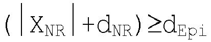

- The method of manufacturing a semiconductor device according to claim 10,
wherein the impurity concentration of the second semiconductor region is 1×10¹⁵ to 1×1022 cm-3. - A power converter comprising a power module configured with the semiconductor device according to claim 1.
- A three-phase motor system that drives a three-phase motor by using the power converter according to claim 12.
- An automobile with wheels driven by the three-phase motor system according to claim 13.
- A railway vehicle with wheels driven by the three-phase motor system according to claim 13.
Applications Claiming Priority (1)
| Application Number | Priority Date | Filing Date | Title |
|---|---|---|---|
| PCT/JP2015/076131 WO2017046868A1 (en) | 2015-09-15 | 2015-09-15 | Semiconductor device and method of manufacturing same, electric power converting device, three-phase motor system, automobile and railway vehicle |
Publications (3)
| Publication Number | Publication Date |
|---|---|
| EP3352225A1 true EP3352225A1 (en) | 2018-07-25 |
| EP3352225A4 EP3352225A4 (en) | 2019-05-22 |
| EP3352225B1 EP3352225B1 (en) | 2023-10-25 |
Family
ID=58288325
Family Applications (1)
| Application Number | Title | Priority Date | Filing Date |
|---|---|---|---|
| EP15904057.5A Active EP3352225B1 (en) | 2015-09-15 | 2015-09-15 | Semiconductor device and method of manufacturing same, electric power converting device, three-phase motor system, automobile and railway vehicle |
Country Status (4)
| Country | Link |
|---|---|
| US (1) | US10236370B2 (en) |
| EP (1) | EP3352225B1 (en) |
| JP (1) | JP6564046B2 (en) |
| WO (1) | WO2017046868A1 (en) |
Cited By (1)
| Publication number | Priority date | Publication date | Assignee | Title |
|---|---|---|---|---|
| CN109390333A (en) * | 2017-08-04 | 2019-02-26 | 艾普凌科有限公司 | Semiconductor device |
Families Citing this family (8)
| Publication number | Priority date | Publication date | Assignee | Title |
|---|---|---|---|---|
| JP7043750B2 (en) * | 2017-07-14 | 2022-03-30 | 株式会社デンソー | SiC- MOSFET |
| JP6953876B2 (en) * | 2017-08-04 | 2021-10-27 | 富士電機株式会社 | Silicon Carbide Semiconductor Device and Method for Manufacturing Silicon Carbide Semiconductor Device |
| DE102017119568B4 (en) | 2017-08-25 | 2024-01-04 | Infineon Technologies Ag | Silicon carbide components and method for producing silicon carbide components |
| CN113053696A (en) * | 2019-12-26 | 2021-06-29 | 施耐德电气工业公司 | Control circuit for contactor and control method thereof |
| US11973116B2 (en) | 2021-05-10 | 2024-04-30 | Kabushiki Kaisha Toshiba | Semiconductor device |
| CN115188810A (en) * | 2022-06-22 | 2022-10-14 | 上海瞻芯电子科技有限公司 | Method for manufacturing silicon carbide device with terminal protection structure |
| CN115241069B (en) * | 2022-06-22 | 2025-09-26 | 上海瞻芯电子科技有限公司 | Method for manufacturing silicon carbide device with terminal protection structure |
| JP2024067415A (en) * | 2022-11-04 | 2024-05-17 | 富士電機株式会社 | Silicon carbide semiconductor device and method for manufacturing silicon carbide semiconductor device |
Family Cites Families (17)
| Publication number | Priority date | Publication date | Assignee | Title |
|---|---|---|---|---|
| JP4422470B2 (en) * | 2003-12-10 | 2010-02-24 | トヨタ自動車株式会社 | Semiconductor device |
| US7737469B2 (en) * | 2006-05-16 | 2010-06-15 | Kabushiki Kaisha Toshiba | Semiconductor device having superjunction structure formed of p-type and n-type pillar regions |
| US7633120B2 (en) * | 2006-08-08 | 2009-12-15 | Alph & Omega Semiconductor, Ltd. | Inverted-trench grounded-source field effect transistor (FET) structure using highly conductive substrates |
| US7741200B2 (en) * | 2006-12-01 | 2010-06-22 | Applied Materials, Inc. | Formation and treatment of epitaxial layer containing silicon and carbon |
| JP4621708B2 (en) * | 2007-05-24 | 2011-01-26 | 株式会社東芝 | Semiconductor device and manufacturing method thereof |
| JP2009094433A (en) * | 2007-10-12 | 2009-04-30 | National Institute Of Advanced Industrial & Technology | Silicon carbide device |
| US8124983B2 (en) * | 2008-08-28 | 2012-02-28 | Infineon Technologies Ag | Power transistor |
| CN102473645B (en) * | 2009-08-19 | 2013-07-10 | 松下电器产业株式会社 | Semiconductor element, semiconductor device, and electric power converter |
| US8492836B2 (en) * | 2009-10-14 | 2013-07-23 | Mitsubishi Electric Corporation | Power semiconductor device |
| JP5172916B2 (en) | 2010-09-08 | 2013-03-27 | 株式会社東芝 | Semiconductor rectifier |
| JP2012074441A (en) | 2010-09-28 | 2012-04-12 | Toshiba Corp | Semiconductor device for power |
| JP5999748B2 (en) * | 2011-08-12 | 2016-09-28 | ルネサスエレクトロニクス株式会社 | Power MOSFET, IGBT and power diode |
| WO2013100155A1 (en) | 2011-12-28 | 2013-07-04 | 富士電機株式会社 | Semiconductor device and method for producing semiconductor device |
| JP2013219150A (en) * | 2012-04-06 | 2013-10-24 | National Institute Of Advanced Industrial & Technology | Manufacturing method of ohmic electrode of silicon carbide semiconductor device |
| JP6065303B2 (en) * | 2012-06-15 | 2017-01-25 | ローム株式会社 | Switching device |
| US9209292B2 (en) * | 2013-07-18 | 2015-12-08 | Infineon Technologies Austria Ag | Charge compensation semiconductor devices |
| JP6379778B2 (en) * | 2014-07-15 | 2018-08-29 | 富士電機株式会社 | Semiconductor device and manufacturing method of semiconductor device |
-
2015
- 2015-09-15 JP JP2017540373A patent/JP6564046B2/en active Active
- 2015-09-15 US US15/759,790 patent/US10236370B2/en active Active
- 2015-09-15 EP EP15904057.5A patent/EP3352225B1/en active Active
- 2015-09-15 WO PCT/JP2015/076131 patent/WO2017046868A1/en not_active Ceased
Cited By (1)
| Publication number | Priority date | Publication date | Assignee | Title |
|---|---|---|---|---|
| CN109390333A (en) * | 2017-08-04 | 2019-02-26 | 艾普凌科有限公司 | Semiconductor device |
Also Published As
| Publication number | Publication date |
|---|---|
| EP3352225B1 (en) | 2023-10-25 |
| JP6564046B2 (en) | 2019-08-21 |
| WO2017046868A1 (en) | 2017-03-23 |
| US10236370B2 (en) | 2019-03-19 |
| JPWO2017046868A1 (en) | 2018-04-19 |
| US20180350973A1 (en) | 2018-12-06 |
| EP3352225A4 (en) | 2019-05-22 |
Similar Documents
| Publication | Publication Date | Title |
|---|---|---|
| EP3352225B1 (en) | Semiconductor device and method of manufacturing same, electric power converting device, three-phase motor system, automobile and railway vehicle | |
| US9312332B2 (en) | Semiconductor device and method for manufacturing the same | |
| US10290704B2 (en) | Semiconductor device and method for manufacturing same, power conversion device, three-phase motor system, automobile, and railway carriage | |
| EP3046149B1 (en) | Semiconductor device, method for manufacturing same, power conversion apparatus, three-phase motor system, automobile, and rail vehicle | |
| JP6514338B2 (en) | Semiconductor device, power module, power converter, automobile and railway vehicle | |
| US10790386B2 (en) | Silicon carbide semiconductor device with horizontal and vertical current flow | |
| JP6290457B2 (en) | Semiconductor device and manufacturing method thereof, power conversion device, three-phase motor system, automobile, and railway vehicle | |
| TW201709522A (en) | Semiconductor device | |
| US20230139229A1 (en) | Semiconductor device and power converter | |
| CN113330579B (en) | Semiconductor devices and power conversion devices | |
| WO2015177914A1 (en) | Semiconductor device, semiconductor device manufacturing method, power conversion device, three-phase motor system, automobile, and train car | |
| WO2016002057A1 (en) | Semiconductor device, power module, power conversion device, three-phase motor system, automobile, and railway vehicle | |
| JP6273020B2 (en) | Semiconductor device, power module, power conversion device, automobile and railway vehicle | |
| WO2015189929A1 (en) | Semiconductor device, power module, power conversion device, and semiconductor device manufacturing method | |
| WO2016002083A1 (en) | Semiconductor device, power module and electric power converter | |
| JP6592083B2 (en) | Semiconductor device, manufacturing method thereof, and power module | |
| JP7002998B2 (en) | Semiconductor devices and their manufacturing methods, power conversion devices, three-phase motor systems, automobiles, and railroad vehicles | |
| JP2018037621A (en) | Semiconductor device, method for manufacturing the same, and power conversion device | |
| WO2017042963A1 (en) | Semiconductor device, method for manufacturing same, power module, power conversion device, and rail vehicle | |
| JP6584940B2 (en) | Manufacturing method of semiconductor device | |
| CN116368623B (en) | Semiconductor device and power conversion device | |
| JP2018046127A (en) | Semiconductor device, power module and electric power conversion device | |
| CN117693818A (en) | Semiconductor device, power conversion device, and method of manufacturing semiconductor device | |
| US10084046B1 (en) | Semiconductor device, inverter circuit, drive device, vehicle, and elevating machine | |
| JP7607834B1 (en) | Semiconductor device, semiconductor device manufacturing method, and power conversion device |
Legal Events
| Date | Code | Title | Description |
|---|---|---|---|
| STAA | Information on the status of an ep patent application or granted ep patent |
Free format text: STATUS: THE INTERNATIONAL PUBLICATION HAS BEEN MADE |
|
| PUAI | Public reference made under article 153(3) epc to a published international application that has entered the european phase |
Free format text: ORIGINAL CODE: 0009012 |
|
| STAA | Information on the status of an ep patent application or granted ep patent |
Free format text: STATUS: REQUEST FOR EXAMINATION WAS MADE |
|
| 17P | Request for examination filed |
Effective date: 20180307 |
|
| AK | Designated contracting states |
Kind code of ref document: A1 Designated state(s): AL AT BE BG CH CY CZ DE DK EE ES FI FR GB GR HR HU IE IS IT LI LT LU LV MC MK MT NL NO PL PT RO RS SE SI SK SM TR |
|
| AX | Request for extension of the european patent |
Extension state: BA ME |
|
| DAV | Request for validation of the european patent (deleted) | ||
| DAX | Request for extension of the european patent (deleted) | ||
| A4 | Supplementary search report drawn up and despatched |
Effective date: 20190424 |
|
| RIC1 | Information provided on ipc code assigned before grant |
Ipc: H01L 29/12 20060101ALI20190416BHEP Ipc: H01L 29/06 20060101ALI20190416BHEP Ipc: H01L 29/78 20060101AFI20190416BHEP Ipc: H01L 21/336 20060101ALI20190416BHEP |
|
| STAA | Information on the status of an ep patent application or granted ep patent |
Free format text: STATUS: EXAMINATION IS IN PROGRESS |
|
| 17Q | First examination report despatched |
Effective date: 20210428 |
|
| GRAP | Despatch of communication of intention to grant a patent |
Free format text: ORIGINAL CODE: EPIDOSNIGR1 |
|
| STAA | Information on the status of an ep patent application or granted ep patent |
Free format text: STATUS: GRANT OF PATENT IS INTENDED |
|
| INTG | Intention to grant announced |
Effective date: 20230203 |
|
| GRAJ | Information related to disapproval of communication of intention to grant by the applicant or resumption of examination proceedings by the epo deleted |
Free format text: ORIGINAL CODE: EPIDOSDIGR1 |
|
| STAA | Information on the status of an ep patent application or granted ep patent |
Free format text: STATUS: EXAMINATION IS IN PROGRESS |
|
| INTC | Intention to grant announced (deleted) | ||
| GRAP | Despatch of communication of intention to grant a patent |
Free format text: ORIGINAL CODE: EPIDOSNIGR1 |
|
| STAA | Information on the status of an ep patent application or granted ep patent |
Free format text: STATUS: GRANT OF PATENT IS INTENDED |
|
| INTG | Intention to grant announced |
Effective date: 20230607 |
|
| GRAS | Grant fee paid |
Free format text: ORIGINAL CODE: EPIDOSNIGR3 |
|
| GRAA | (expected) grant |
Free format text: ORIGINAL CODE: 0009210 |
|
| STAA | Information on the status of an ep patent application or granted ep patent |
Free format text: STATUS: THE PATENT HAS BEEN GRANTED |
|
| AK | Designated contracting states |
Kind code of ref document: B1 Designated state(s): AL AT BE BG CH CY CZ DE DK EE ES FI FR GB GR HR HU IE IS IT LI LT LU LV MC MK MT NL NO PL PT RO RS SE SI SK SM TR |
|
| REG | Reference to a national code |
Ref country code: GB Ref legal event code: FG4D |
|
| REG | Reference to a national code |
Ref country code: CH Ref legal event code: EP |
|
| REG | Reference to a national code |
Ref country code: DE Ref legal event code: R096 Ref document number: 602015086267 Country of ref document: DE |
|
| REG | Reference to a national code |
Ref country code: IE Ref legal event code: FG4D |
|
| REG | Reference to a national code |
Ref country code: LT Ref legal event code: MG9D |
|
| REG | Reference to a national code |
Ref country code: NL Ref legal event code: MP Effective date: 20231025 |
|
| REG | Reference to a national code |
Ref country code: AT Ref legal event code: MK05 Ref document number: 1625579 Country of ref document: AT Kind code of ref document: T Effective date: 20231025 |
|
| PG25 | Lapsed in a contracting state [announced via postgrant information from national office to epo] |
Ref country code: NL Free format text: LAPSE BECAUSE OF FAILURE TO SUBMIT A TRANSLATION OF THE DESCRIPTION OR TO PAY THE FEE WITHIN THE PRESCRIBED TIME-LIMIT Effective date: 20231025 |
|
| PG25 | Lapsed in a contracting state [announced via postgrant information from national office to epo] |
Ref country code: GR Free format text: LAPSE BECAUSE OF FAILURE TO SUBMIT A TRANSLATION OF THE DESCRIPTION OR TO PAY THE FEE WITHIN THE PRESCRIBED TIME-LIMIT Effective date: 20240126 |
|
| PG25 | Lapsed in a contracting state [announced via postgrant information from national office to epo] |
Ref country code: IS Free format text: LAPSE BECAUSE OF FAILURE TO SUBMIT A TRANSLATION OF THE DESCRIPTION OR TO PAY THE FEE WITHIN THE PRESCRIBED TIME-LIMIT Effective date: 20240225 |
|
| PG25 | Lapsed in a contracting state [announced via postgrant information from national office to epo] |
Ref country code: LT Free format text: LAPSE BECAUSE OF FAILURE TO SUBMIT A TRANSLATION OF THE DESCRIPTION OR TO PAY THE FEE WITHIN THE PRESCRIBED TIME-LIMIT Effective date: 20231025 |
|
| PG25 | Lapsed in a contracting state [announced via postgrant information from national office to epo] |
Ref country code: AT Free format text: LAPSE BECAUSE OF FAILURE TO SUBMIT A TRANSLATION OF THE DESCRIPTION OR TO PAY THE FEE WITHIN THE PRESCRIBED TIME-LIMIT Effective date: 20231025 |
|
| PG25 | Lapsed in a contracting state [announced via postgrant information from national office to epo] |
Ref country code: ES Free format text: LAPSE BECAUSE OF FAILURE TO SUBMIT A TRANSLATION OF THE DESCRIPTION OR TO PAY THE FEE WITHIN THE PRESCRIBED TIME-LIMIT Effective date: 20231025 |
|
| PG25 | Lapsed in a contracting state [announced via postgrant information from national office to epo] |
Ref country code: LT Free format text: LAPSE BECAUSE OF FAILURE TO SUBMIT A TRANSLATION OF THE DESCRIPTION OR TO PAY THE FEE WITHIN THE PRESCRIBED TIME-LIMIT Effective date: 20231025 Ref country code: IS Free format text: LAPSE BECAUSE OF FAILURE TO SUBMIT A TRANSLATION OF THE DESCRIPTION OR TO PAY THE FEE WITHIN THE PRESCRIBED TIME-LIMIT Effective date: 20240225 Ref country code: GR Free format text: LAPSE BECAUSE OF FAILURE TO SUBMIT A TRANSLATION OF THE DESCRIPTION OR TO PAY THE FEE WITHIN THE PRESCRIBED TIME-LIMIT Effective date: 20240126 Ref country code: ES Free format text: LAPSE BECAUSE OF FAILURE TO SUBMIT A TRANSLATION OF THE DESCRIPTION OR TO PAY THE FEE WITHIN THE PRESCRIBED TIME-LIMIT Effective date: 20231025 Ref country code: BG Free format text: LAPSE BECAUSE OF FAILURE TO SUBMIT A TRANSLATION OF THE DESCRIPTION OR TO PAY THE FEE WITHIN THE PRESCRIBED TIME-LIMIT Effective date: 20240125 Ref country code: AT Free format text: LAPSE BECAUSE OF FAILURE TO SUBMIT A TRANSLATION OF THE DESCRIPTION OR TO PAY THE FEE WITHIN THE PRESCRIBED TIME-LIMIT Effective date: 20231025 Ref country code: PT Free format text: LAPSE BECAUSE OF FAILURE TO SUBMIT A TRANSLATION OF THE DESCRIPTION OR TO PAY THE FEE WITHIN THE PRESCRIBED TIME-LIMIT Effective date: 20240226 |
|
| PG25 | Lapsed in a contracting state [announced via postgrant information from national office to epo] |
Ref country code: SE Free format text: LAPSE BECAUSE OF FAILURE TO SUBMIT A TRANSLATION OF THE DESCRIPTION OR TO PAY THE FEE WITHIN THE PRESCRIBED TIME-LIMIT Effective date: 20231025 Ref country code: RS Free format text: LAPSE BECAUSE OF FAILURE TO SUBMIT A TRANSLATION OF THE DESCRIPTION OR TO PAY THE FEE WITHIN THE PRESCRIBED TIME-LIMIT Effective date: 20231025 Ref country code: PL Free format text: LAPSE BECAUSE OF FAILURE TO SUBMIT A TRANSLATION OF THE DESCRIPTION OR TO PAY THE FEE WITHIN THE PRESCRIBED TIME-LIMIT Effective date: 20231025 Ref country code: NO Free format text: LAPSE BECAUSE OF FAILURE TO SUBMIT A TRANSLATION OF THE DESCRIPTION OR TO PAY THE FEE WITHIN THE PRESCRIBED TIME-LIMIT Effective date: 20240125 Ref country code: LV Free format text: LAPSE BECAUSE OF FAILURE TO SUBMIT A TRANSLATION OF THE DESCRIPTION OR TO PAY THE FEE WITHIN THE PRESCRIBED TIME-LIMIT Effective date: 20231025 Ref country code: HR Free format text: LAPSE BECAUSE OF FAILURE TO SUBMIT A TRANSLATION OF THE DESCRIPTION OR TO PAY THE FEE WITHIN THE PRESCRIBED TIME-LIMIT Effective date: 20231025 |
|
| PG25 | Lapsed in a contracting state [announced via postgrant information from national office to epo] |
Ref country code: DK Free format text: LAPSE BECAUSE OF FAILURE TO SUBMIT A TRANSLATION OF THE DESCRIPTION OR TO PAY THE FEE WITHIN THE PRESCRIBED TIME-LIMIT Effective date: 20231025 |
|
| PG25 | Lapsed in a contracting state [announced via postgrant information from national office to epo] |
Ref country code: CZ Free format text: LAPSE BECAUSE OF FAILURE TO SUBMIT A TRANSLATION OF THE DESCRIPTION OR TO PAY THE FEE WITHIN THE PRESCRIBED TIME-LIMIT Effective date: 20231025 |
|
| REG | Reference to a national code |
Ref country code: DE Ref legal event code: R097 Ref document number: 602015086267 Country of ref document: DE |
|
| PG25 | Lapsed in a contracting state [announced via postgrant information from national office to epo] |
Ref country code: SK Free format text: LAPSE BECAUSE OF FAILURE TO SUBMIT A TRANSLATION OF THE DESCRIPTION OR TO PAY THE FEE WITHIN THE PRESCRIBED TIME-LIMIT Effective date: 20231025 |
|
| PG25 | Lapsed in a contracting state [announced via postgrant information from national office to epo] |
Ref country code: SM Free format text: LAPSE BECAUSE OF FAILURE TO SUBMIT A TRANSLATION OF THE DESCRIPTION OR TO PAY THE FEE WITHIN THE PRESCRIBED TIME-LIMIT Effective date: 20231025 Ref country code: SK Free format text: LAPSE BECAUSE OF FAILURE TO SUBMIT A TRANSLATION OF THE DESCRIPTION OR TO PAY THE FEE WITHIN THE PRESCRIBED TIME-LIMIT Effective date: 20231025 Ref country code: RO Free format text: LAPSE BECAUSE OF FAILURE TO SUBMIT A TRANSLATION OF THE DESCRIPTION OR TO PAY THE FEE WITHIN THE PRESCRIBED TIME-LIMIT Effective date: 20231025 Ref country code: IT Free format text: LAPSE BECAUSE OF FAILURE TO SUBMIT A TRANSLATION OF THE DESCRIPTION OR TO PAY THE FEE WITHIN THE PRESCRIBED TIME-LIMIT Effective date: 20231025 Ref country code: EE Free format text: LAPSE BECAUSE OF FAILURE TO SUBMIT A TRANSLATION OF THE DESCRIPTION OR TO PAY THE FEE WITHIN THE PRESCRIBED TIME-LIMIT Effective date: 20231025 Ref country code: DK Free format text: LAPSE BECAUSE OF FAILURE TO SUBMIT A TRANSLATION OF THE DESCRIPTION OR TO PAY THE FEE WITHIN THE PRESCRIBED TIME-LIMIT Effective date: 20231025 Ref country code: CZ Free format text: LAPSE BECAUSE OF FAILURE TO SUBMIT A TRANSLATION OF THE DESCRIPTION OR TO PAY THE FEE WITHIN THE PRESCRIBED TIME-LIMIT Effective date: 20231025 |
|
| PLBE | No opposition filed within time limit |
Free format text: ORIGINAL CODE: 0009261 |
|
| STAA | Information on the status of an ep patent application or granted ep patent |
Free format text: STATUS: NO OPPOSITION FILED WITHIN TIME LIMIT |
|
| 26N | No opposition filed |
Effective date: 20240726 |
|
| PG25 | Lapsed in a contracting state [announced via postgrant information from national office to epo] |
Ref country code: SI Free format text: LAPSE BECAUSE OF FAILURE TO SUBMIT A TRANSLATION OF THE DESCRIPTION OR TO PAY THE FEE WITHIN THE PRESCRIBED TIME-LIMIT Effective date: 20231025 |
|
| PG25 | Lapsed in a contracting state [announced via postgrant information from national office to epo] |
Ref country code: SI Free format text: LAPSE BECAUSE OF FAILURE TO SUBMIT A TRANSLATION OF THE DESCRIPTION OR TO PAY THE FEE WITHIN THE PRESCRIBED TIME-LIMIT Effective date: 20231025 |
|
| REG | Reference to a national code |
Ref country code: DE Ref legal event code: R079 Ref document number: 602015086267 Country of ref document: DE Free format text: PREVIOUS MAIN CLASS: H01L0029780000 Ipc: H10D0030600000 |
|
| PG25 | Lapsed in a contracting state [announced via postgrant information from national office to epo] |
Ref country code: MC Free format text: LAPSE BECAUSE OF FAILURE TO SUBMIT A TRANSLATION OF THE DESCRIPTION OR TO PAY THE FEE WITHIN THE PRESCRIBED TIME-LIMIT Effective date: 20231025 |
|
| REG | Reference to a national code |
Ref country code: CH Ref legal event code: PL |
|
| PG25 | Lapsed in a contracting state [announced via postgrant information from national office to epo] |
Ref country code: LU Free format text: LAPSE BECAUSE OF NON-PAYMENT OF DUE FEES Effective date: 20240915 |
|
| GBPC | Gb: european patent ceased through non-payment of renewal fee |
Effective date: 20240915 |
|
| PG25 | Lapsed in a contracting state [announced via postgrant information from national office to epo] |
Ref country code: GB Free format text: LAPSE BECAUSE OF NON-PAYMENT OF DUE FEES Effective date: 20240915 |
|
| REG | Reference to a national code |
Ref country code: BE Ref legal event code: MM Effective date: 20240930 |
|
| PG25 | Lapsed in a contracting state [announced via postgrant information from national office to epo] |
Ref country code: BE Free format text: LAPSE BECAUSE OF NON-PAYMENT OF DUE FEES Effective date: 20240930 |
|
| PG25 | Lapsed in a contracting state [announced via postgrant information from national office to epo] |
Ref country code: FR Free format text: LAPSE BECAUSE OF NON-PAYMENT OF DUE FEES Effective date: 20240930 |
|
| PG25 | Lapsed in a contracting state [announced via postgrant information from national office to epo] |
Ref country code: CH Free format text: LAPSE BECAUSE OF NON-PAYMENT OF DUE FEES Effective date: 20240930 |
|
| PG25 | Lapsed in a contracting state [announced via postgrant information from national office to epo] |
Ref country code: IE Free format text: LAPSE BECAUSE OF NON-PAYMENT OF DUE FEES Effective date: 20240915 |
|
| PG25 | Lapsed in a contracting state [announced via postgrant information from national office to epo] |
Ref country code: FI Free format text: LAPSE BECAUSE OF FAILURE TO SUBMIT A TRANSLATION OF THE DESCRIPTION OR TO PAY THE FEE WITHIN THE PRESCRIBED TIME-LIMIT Effective date: 20231025 |
|
| PGFP | Annual fee paid to national office [announced via postgrant information from national office to epo] |
Ref country code: DE Payment date: 20250730 Year of fee payment: 11 |
|
| PG25 | Lapsed in a contracting state [announced via postgrant information from national office to epo] |
Ref country code: CY Free format text: LAPSE BECAUSE OF FAILURE TO SUBMIT A TRANSLATION OF THE DESCRIPTION OR TO PAY THE FEE WITHIN THE PRESCRIBED TIME-LIMIT; INVALID AB INITIO Effective date: 20150915 |
|
| PG25 | Lapsed in a contracting state [announced via postgrant information from national office to epo] |
Ref country code: HU Free format text: LAPSE BECAUSE OF FAILURE TO SUBMIT A TRANSLATION OF THE DESCRIPTION OR TO PAY THE FEE WITHIN THE PRESCRIBED TIME-LIMIT; INVALID AB INITIO Effective date: 20150915 |
|
| PG25 | Lapsed in a contracting state [announced via postgrant information from national office to epo] |
Ref country code: TR Free format text: LAPSE BECAUSE OF FAILURE TO SUBMIT A TRANSLATION OF THE DESCRIPTION OR TO PAY THE FEE WITHIN THE PRESCRIBED TIME-LIMIT Effective date: 20231025 |