EP3349342A1 - Switch power supply and primary control chip thereof, and loop compensation apparatus - Google Patents
Switch power supply and primary control chip thereof, and loop compensation apparatus Download PDFInfo
- Publication number
- EP3349342A1 EP3349342A1 EP16843622.8A EP16843622A EP3349342A1 EP 3349342 A1 EP3349342 A1 EP 3349342A1 EP 16843622 A EP16843622 A EP 16843622A EP 3349342 A1 EP3349342 A1 EP 3349342A1
- Authority
- EP
- European Patent Office
- Prior art keywords
- power supply
- loop compensation
- switching
- output end
- generation circuit
- Prior art date
- Legal status (The legal status is an assumption and is not a legal conclusion. Google has not performed a legal analysis and makes no representation as to the accuracy of the status listed.)
- Withdrawn
Links
- 239000003990 capacitor Substances 0.000 claims abstract description 61
- 230000003321 amplification Effects 0.000 claims abstract description 12
- 238000003199 nucleic acid amplification method Methods 0.000 claims abstract description 12
- 230000002596 correlated effect Effects 0.000 claims description 4
- 230000005347 demagnetization Effects 0.000 description 10
- 238000010586 diagram Methods 0.000 description 9
- 238000005070 sampling Methods 0.000 description 7
- HCUOEKSZWPGJIM-YBRHCDHNSA-N (e,2e)-2-hydroxyimino-6-methoxy-4-methyl-5-nitrohex-3-enamide Chemical compound COCC([N+]([O-])=O)\C(C)=C\C(=N/O)\C(N)=O HCUOEKSZWPGJIM-YBRHCDHNSA-N 0.000 description 5
- 101100162200 Aspergillus parasiticus (strain ATCC 56775 / NRRL 5862 / SRRC 143 / SU-1) aflD gene Proteins 0.000 description 5
- 238000004804 winding Methods 0.000 description 5
- 238000007599 discharging Methods 0.000 description 4
- 101100397044 Xenopus laevis invs-a gene Proteins 0.000 description 3
- 101100397045 Xenopus laevis invs-b gene Proteins 0.000 description 3
- 230000001276 controlling effect Effects 0.000 description 3
- 239000000463 material Substances 0.000 description 2
- 229910044991 metal oxide Inorganic materials 0.000 description 2
- 150000004706 metal oxides Chemical class 0.000 description 2
- 239000004065 semiconductor Substances 0.000 description 2
- 230000019771 cognition Effects 0.000 description 1
- 230000006870 function Effects 0.000 description 1
- 238000000034 method Methods 0.000 description 1
- 238000012986 modification Methods 0.000 description 1
- 230000004048 modification Effects 0.000 description 1
- 230000000737 periodic effect Effects 0.000 description 1
- 238000006467 substitution reaction Methods 0.000 description 1
Images




Classifications
-
- H—ELECTRICITY
- H02—GENERATION; CONVERSION OR DISTRIBUTION OF ELECTRIC POWER
- H02M—APPARATUS FOR CONVERSION BETWEEN AC AND AC, BETWEEN AC AND DC, OR BETWEEN DC AND DC, AND FOR USE WITH MAINS OR SIMILAR POWER SUPPLY SYSTEMS; CONVERSION OF DC OR AC INPUT POWER INTO SURGE OUTPUT POWER; CONTROL OR REGULATION THEREOF
- H02M1/00—Details of apparatus for conversion
- H02M1/14—Arrangements for reducing ripples from DC input or output
-
- H—ELECTRICITY
- H02—GENERATION; CONVERSION OR DISTRIBUTION OF ELECTRIC POWER
- H02M—APPARATUS FOR CONVERSION BETWEEN AC AND AC, BETWEEN AC AND DC, OR BETWEEN DC AND DC, AND FOR USE WITH MAINS OR SIMILAR POWER SUPPLY SYSTEMS; CONVERSION OF DC OR AC INPUT POWER INTO SURGE OUTPUT POWER; CONTROL OR REGULATION THEREOF
- H02M1/00—Details of apparatus for conversion
- H02M1/08—Circuits specially adapted for the generation of control voltages for semiconductor devices incorporated in static converters
-
- H—ELECTRICITY
- H02—GENERATION; CONVERSION OR DISTRIBUTION OF ELECTRIC POWER
- H02M—APPARATUS FOR CONVERSION BETWEEN AC AND AC, BETWEEN AC AND DC, OR BETWEEN DC AND DC, AND FOR USE WITH MAINS OR SIMILAR POWER SUPPLY SYSTEMS; CONVERSION OF DC OR AC INPUT POWER INTO SURGE OUTPUT POWER; CONTROL OR REGULATION THEREOF
- H02M1/00—Details of apparatus for conversion
- H02M1/42—Circuits or arrangements for compensating for or adjusting power factor in converters or inverters
- H02M1/4208—Arrangements for improving power factor of AC input
- H02M1/4258—Arrangements for improving power factor of AC input using a single converter stage both for correction of AC input power factor and generation of a regulated and galvanically isolated DC output voltage
-
- H—ELECTRICITY
- H02—GENERATION; CONVERSION OR DISTRIBUTION OF ELECTRIC POWER
- H02M—APPARATUS FOR CONVERSION BETWEEN AC AND AC, BETWEEN AC AND DC, OR BETWEEN DC AND DC, AND FOR USE WITH MAINS OR SIMILAR POWER SUPPLY SYSTEMS; CONVERSION OF DC OR AC INPUT POWER INTO SURGE OUTPUT POWER; CONTROL OR REGULATION THEREOF
- H02M3/00—Conversion of DC power input into DC power output
- H02M3/02—Conversion of DC power input into DC power output without intermediate conversion into AC
- H02M3/04—Conversion of DC power input into DC power output without intermediate conversion into AC by static converters
- H02M3/10—Conversion of DC power input into DC power output without intermediate conversion into AC by static converters using discharge tubes with control electrode or semiconductor devices with control electrode
- H02M3/145—Conversion of DC power input into DC power output without intermediate conversion into AC by static converters using discharge tubes with control electrode or semiconductor devices with control electrode using devices of a triode or transistor type requiring continuous application of a control signal
- H02M3/155—Conversion of DC power input into DC power output without intermediate conversion into AC by static converters using discharge tubes with control electrode or semiconductor devices with control electrode using devices of a triode or transistor type requiring continuous application of a control signal using semiconductor devices only
- H02M3/156—Conversion of DC power input into DC power output without intermediate conversion into AC by static converters using discharge tubes with control electrode or semiconductor devices with control electrode using devices of a triode or transistor type requiring continuous application of a control signal using semiconductor devices only with automatic control of output voltage or current, e.g. switching regulators
-
- H—ELECTRICITY
- H02—GENERATION; CONVERSION OR DISTRIBUTION OF ELECTRIC POWER
- H02M—APPARATUS FOR CONVERSION BETWEEN AC AND AC, BETWEEN AC AND DC, OR BETWEEN DC AND DC, AND FOR USE WITH MAINS OR SIMILAR POWER SUPPLY SYSTEMS; CONVERSION OF DC OR AC INPUT POWER INTO SURGE OUTPUT POWER; CONTROL OR REGULATION THEREOF
- H02M3/00—Conversion of DC power input into DC power output
- H02M3/22—Conversion of DC power input into DC power output with intermediate conversion into AC
- H02M3/24—Conversion of DC power input into DC power output with intermediate conversion into AC by static converters
- H02M3/28—Conversion of DC power input into DC power output with intermediate conversion into AC by static converters using discharge tubes with control electrode or semiconductor devices with control electrode to produce the intermediate AC
- H02M3/325—Conversion of DC power input into DC power output with intermediate conversion into AC by static converters using discharge tubes with control electrode or semiconductor devices with control electrode to produce the intermediate AC using devices of a triode or a transistor type requiring continuous application of a control signal
- H02M3/335—Conversion of DC power input into DC power output with intermediate conversion into AC by static converters using discharge tubes with control electrode or semiconductor devices with control electrode to produce the intermediate AC using devices of a triode or a transistor type requiring continuous application of a control signal using semiconductor devices only
- H02M3/33507—Conversion of DC power input into DC power output with intermediate conversion into AC by static converters using discharge tubes with control electrode or semiconductor devices with control electrode to produce the intermediate AC using devices of a triode or a transistor type requiring continuous application of a control signal using semiconductor devices only with automatic control of the output voltage or current, e.g. flyback converters
- H02M3/33523—Conversion of DC power input into DC power output with intermediate conversion into AC by static converters using discharge tubes with control electrode or semiconductor devices with control electrode to produce the intermediate AC using devices of a triode or a transistor type requiring continuous application of a control signal using semiconductor devices only with automatic control of the output voltage or current, e.g. flyback converters with galvanic isolation between input and output of both the power stage and the feedback loop
-
- H—ELECTRICITY
- H02—GENERATION; CONVERSION OR DISTRIBUTION OF ELECTRIC POWER
- H02M—APPARATUS FOR CONVERSION BETWEEN AC AND AC, BETWEEN AC AND DC, OR BETWEEN DC AND DC, AND FOR USE WITH MAINS OR SIMILAR POWER SUPPLY SYSTEMS; CONVERSION OF DC OR AC INPUT POWER INTO SURGE OUTPUT POWER; CONTROL OR REGULATION THEREOF
- H02M1/00—Details of apparatus for conversion
- H02M1/0003—Details of control, feedback or regulation circuits
- H02M1/0025—Arrangements for modifying reference values, feedback values or error values in the control loop of a converter
Definitions
- the present invention relates to the technical field of charging power supplies, and particularly, relates to a loop compensation device for a switching power supply, a primary control chip with the loop compensation device and a switching power supply.
- Fig. 1 the application circuit diagram of a typical flyback switching power supply is shown as Fig. 1 , in which the feedback sampling of an output is generally achieved by adopting sampling feedback with an auxiliary winding of a transformer.
- Fig. 2 is a structural block diagram of a primary control chip in the typical switching power supply.
- constant voltage of a system is realized in such a way that the secondary voltage is sampled by the auxiliary winding, the sampled output voltage is provided to an error amplifier as an input and is subjected to error amplification with a reference voltage, and the turn-on time and the operation frequency of an external power switch are finally controlled.
- the loop compensation is mainly achieved by adding a compensation capacitor Cea to the output end of the error amplifier.
- the compensation method may result in the problem that the output ripple is too large because the loop cannot be stable within a range from light load to idle load.
- the present invention is aimed to solve one of the technical problems in the relevant art to at least a certain extent.
- the first aim of the present invention is to provide a loop compensation device for a switching power supply, which solves the problem that the output ripple of a system is too large and ensures the loop stability by controlling the output of the error amplifier.
- the second aim of the present invention is to provide a primary control chip for a switching power supply.
- the third aim of the present invention is to provide a switching power supply.
- an embodiment in the first aspect of the present invention provides a loop compensation device for a switching power supply, including: an error amplifier, wherein the first input end of said error amplifier is connected with the output end of a sample and holding circuit of a primary control chip in said switching power supply, the second input end of said error amplifier is connected with a first reference voltage reference end, and the error amplifier is used for obtaining an error amplification signal according to a sample and holding signal of said sample and holding circuit and a first reference voltage signal of the first reference voltage reference end; a switching logic gate, wherein the input end of said switching logic gate is connected with the output end of said error amplifier; a loop compensation capacitor, wherein one end of said loop compensation capacitor is connected with the output end of said switching logic gate, and the other end of said loop compensation capacitor is grounded; and a delay generation circuit, wherein the output end of said delay generation circuit is connected with the control end of said switching logic gate, and the delay generation circuit is used for outputting a valid switching control signal within a preset time after
- the switching logic gate and the delay generation circuit for controlling the switching logic gate are added to the output end of the error amplifier, the delay generation circuit outputs a valid switching control signal within the preset time after the power switch is turned off to control the switching logic gate in a turn-on state, and the loop compensation capacitor is charged/discharged by means of the error amplification signal output by the error amplifier, such that loop compensation is realized in the switching power supply, and the output signal of the error amplifier is controlled via the switching logic gate.
- an embodiment in the second aspect of the present invention provides a primary control chip for a switching power supply, including said loop compensation device for the switching power supply.
- the output signal of the error amplifier can be controlled via the switching logic gate, i.e., the loop compensation capacitor is charged/discharged by means of the output of the error amplifier only within a small period of time, namely the preset time after the power switch is turned off, to realize loop compensation.
- the loop stability under light or idle load of the switching power supply is aimed; the output from the error amplifier can truly reflect the actual condition of the secondary output voltage under extremely low frequency on the premise that the high frequency operation of the switching power supply is not affected.
- the problem that the output ripple from the switching power supply is too large is solved, and the loop stability is ensured.
- an embodiment of the present invention further provides a switching power supply, including said primary control chip for the switching power supply.
- the switching power supply in the embodiment of the present invention is aimed at loop stability under light or idle load, the output from the error amplifier can relatively truly reflect the actual condition of the secondary output voltage under extremely low frequency on the premise that high-frequency operation is not affected. The problem that the output ripple is too large is solved, and the loop stability is ensured.
- the sampling mode with an auxiliary winding of a transformer is intermittent sampling, i.e., after a power switch is turned off, the interior of a primary control chip samples the voltage across the auxiliary winding.
- the voltage across the auxiliary winding can only reflect the output voltage within the secondary demagnetization time TDS, the output voltage can also only be sampled by the primary control chip within the secondary demagnetization time, whereas the feedback input of the error amplifier beyond the sampling time will be held by a sample and holding circuit, i.e., the error amplifier cannot track the change of the output voltage in real time.
- the secondary demagnetization time TDS (NS/NP) ⁇ (1/Vout) ⁇ Lp ⁇ Ip, wherein, NS/NP is a secondary/ primary turn ratio, Vout is the output voltage, Lp is a primary inductance value, and Ip is the primary peak current.
- the operation frequency of the system is often relatively low, the primary peak current is relatively low at the same time, the secondary demagnetization time, i.e., the sampling time, is very short relative to the operation cycle of the system at the moment, thus, the change of the error amplifier is far behind the change of the output voltage such that the loop is difficult to stabilize.
- the instability of the loop the low-frequency ripple will be introduced, the output ripple of the system will be too large, and the specific waveform thereof is shown as Fig. 3 .
- Described below by reference to the accompanying drawings are a loop compensation device for a switching power supply, a primary control chip of the switching power supply with the loop compensation device and the switching power supply according to the embodiments of the present invention.
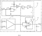
- a loop compensation device for a switching power supply includes an error amplifier 10, a switching logic gate 20, a loop compensation capacitor Cea and a delay generation circuit 30.
- the first input end of the error amplifier 10 is connected with the output end of a sample and holding circuit
- the second input end of the error amplifier 10 is connected with a first reference voltage reference end
- the sample and holding circuit is used for performing sampling and holding the voltage of the output feedback end of the primary control chip in the switching power supply and outputting a sample and holding signal VSH via the output end thereof.
- the first reference voltage reference end provides a first reference voltage signal Vref.
- the error amplifier 10 is used for obtaining an error amplification signal VEA according to the sample and holding signal VSH of the sample and holding circuit and the first reference voltage signal Vref of the first reference voltage reference end, that is to say, the voltage of the output feedback end of the primary control chip in the switching power supply is subjected to sample and holding of the sample and holding circuit to obtain the sample and holding signal VSH, then the voltage is compared with the given reference voltage via the error amplifier 10, and the error amplifier 10 amplifies the error quantity between the sample and holding signal VSH and the first reference voltage signal Vref and outputs it to a subsequent constant voltage and constant current control module to control the operation frequency and duty ratio of the power switch, so as to control the output voltage of the switching power supply.
- the input end of the switching logic gate 20 is connected with the output end of the error amplifier 10, one end of the loop compensation capacitor Cea is connected with the output end of the switching logic gate 20, and the other end of the loop compensation capacitor Cea is grounded.
- the delay generation circuit 30 is mainly used for generating a periodic switching control signal CT.
- CT is valid at the beginning of a cycle (the power switch is turned off), and becomes invalid within a period of time after the power switch is turned off, i.e., a preset time.
- the switching control signal CT controls the switching logic gate 20 connected with the output end of the error amplifier 10.
- the output VEA of the error amplifier 10 is connected to the loop compensation capacitor Cea within the period that the switching control signal CT is valid, and the error amplifier 10 compares the sample and holding signal VSH fed back by the output voltage with the first reference voltage signal Vref and amplifies.
- VSH the error amplifier 10 will discharge the loop compensation capacitor Cea, and the voltage across the loop compensation capacitor Cea drops.
- VSH ⁇ Vref the error amplifier 10 will charge the loop compensation capacitor Cea, and the voltage across the loop compensation capacitor Cea rises.
- the switching control signal CT is valid (CT being valid within the preset time after the power switch is turned off means that the time period from beginning of turn-off of the power switch to the end of the preset time is the valid time, and the remaining time is invalid)
- the output end of the error amplifier 10 is disconnected from the loop compensation capacitor Cea, at the moment, because the charging/discharging path of the loop compensation capacitor Cea is cut off, the voltage value across the loop compensation capacitor Cea will be held till the coming of the valid time of next CT, and the output voltage of the error amplifier 10 is held within a period of time after the power switch is turned off.
- the subsequent circuit such as the constant current and constant voltage control module (e.g., the pulse width modulation (PWM) & pulse frequency modulation (PFM) circuit), a logic control module and an output drive module in the primary control chip controls the operation frequency of the whole switching power supply and the turn-on time of the power switch according to the voltage across the loop compensation capacitor Cea.
- the constant current and constant voltage control module e.g., the pulse width modulation (PWM) & pulse frequency modulation (PFM) circuit
- PWM pulse width modulation
- PFM pulse frequency modulation
- the delay generation circuit 30 generates a valid switching control signal under the control of a trigger signal SIN, wherein the trigger signal SIN may be a turn-off signal for the power switch.
- SIN is a trigger signal for CT and is used for generating a beginning signal for the valid time of the CT, and because the CT becomes invalid within a period of time of delaying after the power switch is turned off, the trigger signal SIN of the delay generation circuit 30 is often the turn-off signal for the power switch.
- SIN may also be a turn-on signal or a demagnetization signal for the power switch, e.g., a turn-on signal ON, a turn-off signal OFF, a drive signal BR1, a logic control signal PUL or a secondary demagnetization signal TDS for the power switch in Fig. 2 .
- the switching logic gate 20 specifically includes a first inverter inv1, a first switch M1 and a second switch M2.
- the input end of the first inverter inv1 is connected with the output end of the delay generation circuit 30, the first end of the first switch M1 is connected with the first end of the second switch M2 and then connected with the output end of the error amplifier 10, the second end of the first switch M1 is connected with the output end of the delay generation circuit 30, the second end of the second switch M2 is connected with the output end of the first inverter inv1, and the third end of the first switch M1 is connected with the third end of the second switch M2 and then serves as the output end of the switching logic gate 20.
- Both the first switch M1 and the second switch M2 are MOS (Metal Oxide Semiconductor) transistors.
- the delay generation circuit 30 specifically includes a first NMOS (N-type Metal Oxide Semiconductor) transistor MN1, a first capacitor C1, a Schmitt trigger 301, a first NOR gate nor1 and a second inverter inv2.
- NMOS N-type Metal Oxide Semiconductor
- the gate of the first NMOS transistor MN1 serves as the trigger end of the delay generation circuit 30 to receive the trigger signal SIN, the drain of the first NMOS transistor MN1 is connected with a first current source II, and the source of the first NMOS transistor MN1 is grounded; the first capacitor C1 is connected in parallel between the drain and the source of the first NMOS transistor MN1, the input end of the Schmitt trigger 301 is connected with the drain of the first NMOS transistor MN1, the first input end of the first NOR gate nor1 is connected with the output end of the Schmitt trigger 301, and the second input end of the first NOR gate nor1 is connected with the gate of the first NMOS transistor MN1; the input end of the second inverter inv2 is connected with the output end of the first NOR gate nor1, and the output end of the second inverter inv2 serves as the output end of the delay generation circuit 30.
- the delay generation circuit 30 specifically includes a second NMOS transistor MN2, a second capacitor C2, a comparator 302, a second NOR gate nor2 and a third inverter inv3.
- the gate of the second NMOS transistor MN2 serves as the trigger end of the delay generation circuit 30 to receive the trigger signal SIN, the drain of the second NMOS transistor MN2 is connected with a second current source 12, and the source of the second NMOS transistor MN2 is grounded; the second capacitor C2 is connected in parallel between the drain and the source of the second NMOS transistor MN2, the negative input end of the comparator 302 is connected with the drain of the second NMOS transistor MN2, the positive input end of the comparator 302 is connected with a second reference voltage reference end, the second reference voltage reference end provides a second reference voltage signal Vref2, the first input end of the second NOR gate nor2 is connected with the output end of the comparator 302, and the second input end of the second NOR gate nor2 is connected with the gate of the second NMOS transistor MN2; the input end of the third inverter inv3 is connected with the output end of the second NOR gate nor2, and the output end of the third inverter inv3 serves as the output end of
- the secondary demagnetization signal TDS is used as the trigger signal SIN
- Fig. 6 is another circuit implementation scheme of the loop compensation device for the switching power supply in an embodiment of the present invention, wherein the Schmitt trigger 301 in Fig. 5 is substituted by the comparator 302.
- the VEA can follow the change of the output voltage under relatively low frequency, so that loop stability of the switching power supply is effectively promoted.
- the delay generation circuit outputs a valid switching control signal within the preset time after the power switch is turned off to control the switching logic gate in a turn-on state
- the loop compensation capacitor is charged/discharged by means of the error amplification signal outputted from the error amplifier, loop compensation is thus realized in the switching power supply
- the output signal of the error amplifier is controlled via the switching logic gate, i.e., the loop compensation capacitor is charged/discharged by means of the output of the error amplifier only within a small period of time, namely the preset time after the power switch is turned off, to realize loop compensation.
- the loop compensation device for the switching power supply in the embodiment of the present invention mainly aims at the loop stability under the condition of light or idle load.
- the output of the error amplifier can relatively truly reflect the actual situation of the secondary output voltage under very low frequency on the premise that high-frequency operation of the switching power supply is not affected.
- the problem that output ripple of the switching power supply are too large is solved, and the loop stability is ensured.
- an embodiment of the present invention provides a primary control chip for a switching power supply, including said loop compensation device for the switching power supply.
- the output signal of the error amplifier can be controlled via the switching logic gate, i.e., the loop compensation capacitor is charged/discharged by means of the output of the error amplifier only within a small period of time, namely the preset time after the power switch is turned off, to realize loop compensation, so that the loop stability under light or idle load of the switching power supply can be aimed at, and the output of the error amplifier can relatively truly reflect the actual situation of the secondary output voltage under extremelylow frequency on the premise that high-frequency operation of the switching power supply is not affected, The problem that the output ripple from the switching power supply are too large is solved, and the loop stability is ensured.
- an embodiment of the present invention further provides a switching power supply, including said primary control chip for the switching power supply.
- the switching power supply in the embodiment of the present invention aims at the loop stability under light or idle load.
- the output of the error amplifier can relatively truly reflect the actual situation of secondary output voltage under extremely low frequency on the premise that high-frequency operation is not affected, the problem that the output ripple is too large is solved, and the loop stability is ensured.
- first and second are merely for the sake of description, but cannot be understood as indicating or implying the relative importance or implying the quantity of the indicated technical features.
- the features defined with “first” and “second” may explicitly or implicitly include at least one of the features.
- “multiple” means at least two, e.g., two, three, etc., unless otherwise specified.
- the terms “mounted”, “connected”, “fixed” and the like should be understood broadly, e.g., “connected” may be fixedly connected, detachably connected, or integrally connected, may be mechanically connected, or electrically connected, may be directly connected, indirectly connected via a medium, communicating between two elements or interacting between two elements, unless otherwise specified.
- the specific meanings of said terms in the present invention could be understood by those of ordinary skill in the art according to specific circumstance.
- the first feature "on” or “under” the second feature may be direct contact of the first and the second features, or indirect contact of the first and the second features via a medium.
- the first feature "on” , “above” or “upper” the second feature may be the first feature right above or obliquely above of the second feature, or only expresses that the horizontal height of the first feature is higher than that of the second feature.
- the first feature "under”, “below” or “down” the second feature may be the first feature right below or obliquely below the second feature, or only expresses that the horizontal height of the first feature is smaller than that of the second feature.
- references terms “one embodiment”, “some embodiments”, “example”, “specific example”, or “some examples” and the like mean that the specific features, structures, materials or characteristics described in combination with the embodiments or examples are included in at least one embodiment or example of the present application.
- the schematic expression of said terms may not necessarily indicate the same embodiment or example.
- the described specific features, structures, materials or characteristics can be appropriately combined in any or more embodiments or examples.
- different embodiments or examples described in the present specification and the features of the different embodiments or examples can be combined by those skilled in the art without contradiction.
Landscapes
- Engineering & Computer Science (AREA)
- Power Engineering (AREA)
- Dc-Dc Converters (AREA)
Abstract
Description
- The present application claims the priority of Chinese Application No.
201510562897.1, filed on September 7, 2015 - The present invention relates to the technical field of charging power supplies, and particularly, relates to a loop compensation device for a switching power supply, a primary control chip with the loop compensation device and a switching power supply.
- In a relevant art, the application circuit diagram of a typical flyback switching power supply is shown as
Fig. 1 , in which the feedback sampling of an output is generally achieved by adopting sampling feedback with an auxiliary winding of a transformer. Wherein,Fig. 2 is a structural block diagram of a primary control chip in the typical switching power supply. - In combination with
Fig. 1 andFig. 2 , constant voltage of a system is realized in such a way that the secondary voltage is sampled by the auxiliary winding, the sampled output voltage is provided to an error amplifier as an input and is subjected to error amplification with a reference voltage, and the turn-on time and the operation frequency of an external power switch are finally controlled. The loop compensation is mainly achieved by adding a compensation capacitor Cea to the output end of the error amplifier. However, the compensation method may result in the problem that the output ripple is too large because the loop cannot be stable within a range from light load to idle load. - The present invention is aimed to solve one of the technical problems in the relevant art to at least a certain extent. Thus, the first aim of the present invention is to provide a loop compensation device for a switching power supply, which solves the problem that the output ripple of a system is too large and ensures the loop stability by controlling the output of the error amplifier.
- The second aim of the present invention is to provide a primary control chip for a switching power supply. The third aim of the present invention is to provide a switching power supply.
- In order to fulfill the above aims, an embodiment in the first aspect of the present invention provides a loop compensation device for a switching power supply, including: an error amplifier, wherein the first input end of said error amplifier is connected with the output end of a sample and holding circuit of a primary control chip in said switching power supply, the second input end of said error amplifier is connected with a first reference voltage reference end, and the error amplifier is used for obtaining an error amplification signal according to a sample and holding signal of said sample and holding circuit and a first reference voltage signal of the first reference voltage reference end; a switching logic gate, wherein the input end of said switching logic gate is connected with the output end of said error amplifier; a loop compensation capacitor, wherein one end of said loop compensation capacitor is connected with the output end of said switching logic gate, and the other end of said loop compensation capacitor is grounded; and a delay generation circuit, wherein the output end of said delay generation circuit is connected with the control end of said switching logic gate, and the delay generation circuit is used for outputting a valid switching control signal within a preset time after a power switch of the switching power supply is turned off to control said switching logic gate in a turn-on state, so that the loop compensation capacitor is charged/discharged by means of the error amplification signal outputted from said error amplifier.
- According to the loop compensation device for the switching power supply in the embodiment of the present invention, the switching logic gate and the delay generation circuit for controlling the switching logic gate are added to the output end of the error amplifier, the delay generation circuit outputs a valid switching control signal within the preset time after the power switch is turned off to control the switching logic gate in a turn-on state, and the loop compensation capacitor is charged/discharged by means of the error amplification signal output by the error amplifier, such that loop compensation is realized in the switching power supply, and the output signal of the error amplifier is controlled via the switching logic gate.
- In order to fulfill the above aims, an embodiment in the second aspect of the present invention provides a primary control chip for a switching power supply, including said loop compensation device for the switching power supply.
- According to the primary control chip for the switching power supply in the embodiment of the present invention, the output signal of the error amplifier can be controlled via the switching logic gate, i.e., the loop compensation capacitor is charged/discharged by means of the output of the error amplifier only within a small period of time, namely the preset time after the power switch is turned off, to realize loop compensation. Thus the loop stability under light or idle load of the switching power supply is aimed; the output from the error amplifier can truly reflect the actual condition of the secondary output voltage under extremely low frequency on the premise that the high frequency operation of the switching power supply is not affected. The problem that the output ripple from the switching power supply is too large is solved, and the loop stability is ensured.
- Moreover, an embodiment of the present invention further provides a switching power supply, including said primary control chip for the switching power supply.
- The switching power supply in the embodiment of the present invention is aimed at loop stability under light or idle load, the output from the error amplifier can relatively truly reflect the actual condition of the secondary output voltage under extremely low frequency on the premise that high-frequency operation is not affected. The problem that the output ripple is too large is solved, and the loop stability is ensured.
-
-
Fig. 1 is an application circuit diagram of a typical flyback switching power supply in a relevant art; -
Fig. 2 is a structural block diagram of a primary control chip for the switching power supply in the relevant art; -
Fig. 3 is an operation waveform diagram of the typical flyback switching power supply in the relevant art; -
Fig. 4 is a structural block diagram of a loop compensation device for a switching power supply according to an embodiment of the present invention; -
Fig. 5 is a circuit schematic diagram of the loop compensation device for the switching power supply according to a specific embodiment of the present invention; -
Fig. 6 is a circuit schematic diagram of the loop compensation device for the switching power supply according to another specific embodiment of the present invention; and -
Fig. 7 is an operation waveform diagram of the switching power supply according to an embodiment of the present invention. - The embodiments of the present invention will be described in detail below, the examples of the embodiments are shown in the accompanying drawings, and same or similar reference numerals throughout indicate same or similar elements or elements having same or similar functions. The embodiments described below by referring to the drawings are exemplary, and are aimed to interpret the present invention, rather than limiting the present invention.
- The present application is proposed based on inventor's cognition and research on the following problems:
In the relevant art, the sampling mode with an auxiliary winding of a transformer is intermittent sampling, i.e., after a power switch is turned off, the interior of a primary control chip samples the voltage across the auxiliary winding. However, the voltage across the auxiliary winding can only reflect the output voltage within the secondary demagnetization time TDS, the output voltage can also only be sampled by the primary control chip within the secondary demagnetization time, whereas the feedback input of the error amplifier beyond the sampling time will be held by a sample and holding circuit, i.e., the error amplifier cannot track the change of the output voltage in real time. The secondary demagnetization time TDS=(NS/NP)·(1/Vout)·Lp·Ip, wherein, NS/NP is a secondary/ primary turn ratio, Vout is the output voltage, Lp is a primary inductance value, and Ip is the primary peak current. - Within the range from light load to idle load, the operation frequency of the system is often relatively low, the primary peak current is relatively low at the same time, the secondary demagnetization time, i.e., the sampling time, is very short relative to the operation cycle of the system at the moment, thus, the change of the error amplifier is far behind the change of the output voltage such that the loop is difficult to stabilize. With the instability of the loop, the low-frequency ripple will be introduced, the output ripple of the system will be too large, and the specific waveform thereof is shown as
Fig. 3 . - Described below by reference to the accompanying drawings are a loop compensation device for a switching power supply, a primary control chip of the switching power supply with the loop compensation device and the switching power supply according to the embodiments of the present invention.
- As shown in
Fig. 4 , a loop compensation device for a switching power supply according to an embodiment of the present invention includes anerror amplifier 10, aswitching logic gate 20, a loop compensation capacitor Cea and adelay generation circuit 30. - The first input end of the
error amplifier 10 is connected with the output end of a sample and holding circuit, the second input end of theerror amplifier 10 is connected with a first reference voltage reference end, wherein the sample and holding circuit is used for performing sampling and holding the voltage of the output feedback end of the primary control chip in the switching power supply and outputting a sample and holding signal VSH via the output end thereof. The first reference voltage reference end provides a first reference voltage signal Vref. Theerror amplifier 10 is used for obtaining an error amplification signal VEA according to the sample and holding signal VSH of the sample and holding circuit and the first reference voltage signal Vref of the first reference voltage reference end, that is to say, the voltage of the output feedback end of the primary control chip in the switching power supply is subjected to sample and holding of the sample and holding circuit to obtain the sample and holding signal VSH, then the voltage is compared with the given reference voltage via theerror amplifier 10, and theerror amplifier 10 amplifies the error quantity between the sample and holding signal VSH and the first reference voltage signal Vref and outputs it to a subsequent constant voltage and constant current control module to control the operation frequency and duty ratio of the power switch, so as to control the output voltage of the switching power supply. The input end of theswitching logic gate 20 is connected with the output end of theerror amplifier 10, one end of the loop compensation capacitor Cea is connected with the output end of theswitching logic gate 20, and the other end of the loop compensation capacitor Cea is grounded. The output end of thedelay generation circuit 30 is connected with the control end of theswitching logic gate 20, and thedelay generation circuit 30 is used for outputting a valid switching control signal, e.g., CT=1, within a preset time after the power switch of the switching power supply is turned off to control theswitching logic gate 20 in a turn-on state, so that the loop compensation capacitor Cea is charged/discharged by means of the error amplification signal VEA outputted from theerror amplifier 10, to realize loop compensation on the switching power supply. - Moreover, the
delay generation circuit 30 is further used for outputting an invalid switching control signal, e.g., CT=0, beyond the preset time after the power switch is turned off to control theswitching logic gate 20 in a turn-off state, so that the charging/discharging path of the loop compensation capacitor Cea is cut off, and the output voltage of theerror amplifier 10 is held, i.e., the output voltage of theerror amplifier 10 is the voltage of the error amplification signal VEA outputted from theerror amplifier 10 at the moment. - That is to say, in the embodiment of the present invention, the
delay generation circuit 30 is mainly used for generating a periodic switching control signal CT. CT is valid at the beginning of a cycle (the power switch is turned off), and becomes invalid within a period of time after the power switch is turned off, i.e., a preset time. The switching control signal CT controls theswitching logic gate 20 connected with the output end of theerror amplifier 10. The output VEA of theerror amplifier 10 is connected to the loop compensation capacitor Cea within the period that the switching control signal CT is valid, and theerror amplifier 10 compares the sample and holding signal VSH fed back by the output voltage with the first reference voltage signal Vref and amplifies. If VSH>Vref, theerror amplifier 10 will discharge the loop compensation capacitor Cea, and the voltage across the loop compensation capacitor Cea drops. On the contrary, if VSH<Vref, theerror amplifier 10 will charge the loop compensation capacitor Cea, and the voltage across the loop compensation capacitor Cea rises. In addition, if VSH=Vref, theerror amplifier 10 holds the voltage of the output error amplification signal VEA. Beyond the period that the switching control signal CT is valid (CT being valid within the preset time after the power switch is turned off means that the time period from beginning of turn-off of the power switch to the end of the preset time is the valid time, and the remaining time is invalid), the output end of theerror amplifier 10 is disconnected from the loop compensation capacitor Cea, at the moment, because the charging/discharging path of the loop compensation capacitor Cea is cut off, the voltage value across the loop compensation capacitor Cea will be held till the coming of the valid time of next CT, and the output voltage of theerror amplifier 10 is held within a period of time after the power switch is turned off. The subsequent circuit such as the constant current and constant voltage control module (e.g., the pulse width modulation (PWM) & pulse frequency modulation (PFM) circuit), a logic control module and an output drive module in the primary control chip controls the operation frequency of the whole switching power supply and the turn-on time of the power switch according to the voltage across the loop compensation capacitor Cea. - According to an embodiment of the present invention, the
delay generation circuit 30 generates a valid switching control signal under the control of a trigger signal SIN, wherein the trigger signal SIN may be a turn-off signal for the power switch. Specifically, SIN is a trigger signal for CT and is used for generating a beginning signal for the valid time of the CT, and because the CT becomes invalid within a period of time of delaying after the power switch is turned off, the trigger signal SIN of thedelay generation circuit 30 is often the turn-off signal for the power switch. In consideration that the turn-on time of the power switch or the secondary demagnetization time TDS is relatively short and can be ignored within the valid time of the CT, SIN may also be a turn-on signal or a demagnetization signal for the power switch, e.g., a turn-on signal ON, a turn-off signal OFF, a drive signal BR1, a logic control signal PUL or a secondary demagnetization signal TDS for the power switch inFig. 2 . - Specifically, in one embodiment of the present invention, as shown in
Fig. 5 orFig. 6 , theswitching logic gate 20 specifically includes a first inverter inv1, a first switch M1 and a second switch M2. The input end of the first inverter inv1 is connected with the output end of thedelay generation circuit 30, the first end of the first switch M1 is connected with the first end of the second switch M2 and then connected with the output end of theerror amplifier 10, the second end of the first switch M1 is connected with the output end of thedelay generation circuit 30, the second end of the second switch M2 is connected with the output end of the first inverter inv1, and the third end of the first switch M1 is connected with the third end of the second switch M2 and then serves as the output end of the switchinglogic gate 20. Both the first switch M1 and the second switch M2 are MOS (Metal Oxide Semiconductor) transistors. - As shown in
Fig. 5 , thedelay generation circuit 30 specifically includes a first NMOS (N-type Metal Oxide Semiconductor) transistor MN1, a first capacitor C1, aSchmitt trigger 301, a first NOR gate nor1 and a second inverter inv2. The gate of the first NMOS transistor MN1 serves as the trigger end of thedelay generation circuit 30 to receive the trigger signal SIN, the drain of the first NMOS transistor MN1 is connected with a first current source II, and the source of the first NMOS transistor MN1 is grounded; the first capacitor C1 is connected in parallel between the drain and the source of the first NMOS transistor MN1, the input end of theSchmitt trigger 301 is connected with the drain of the first NMOS transistor MN1, the first input end of the first NOR gate nor1 is connected with the output end of theSchmitt trigger 301, and the second input end of the first NOR gate nor1 is connected with the gate of the first NMOS transistor MN1; the input end of the second inverter inv2 is connected with the output end of the first NOR gate nor1, and the output end of the second inverter inv2 serves as the output end of thedelay generation circuit 30. - According to another embodiment of the present invention, as shown in
Fig. 6 , thedelay generation circuit 30 specifically includes a second NMOS transistor MN2, a second capacitor C2, acomparator 302, a second NOR gate nor2 and a third inverter inv3. The gate of the second NMOS transistor MN2 serves as the trigger end of thedelay generation circuit 30 to receive the trigger signal SIN, the drain of the second NMOS transistor MN2 is connected with a secondcurrent source 12, and the source of the second NMOS transistor MN2 is grounded; the second capacitor C2 is connected in parallel between the drain and the source of the second NMOS transistor MN2, the negative input end of thecomparator 302 is connected with the drain of the second NMOS transistor MN2, the positive input end of thecomparator 302 is connected with a second reference voltage reference end, the second reference voltage reference end provides a second reference voltage signal Vref2, the first input end of the second NOR gate nor2 is connected with the output end of thecomparator 302, and the second input end of the second NOR gate nor2 is connected with the gate of the second NMOS transistor MN2; the input end of the third inverter inv3 is connected with the output end of the second NOR gate nor2, and the output end of the third inverter inv3 serves as the output end of thedelay generation circuit 30. - In an example that the secondary demagnetization signal TDS is used as the trigger signal SIN, the secondary demagnetization begins after the power switch is turned off, TDS='1' at the moment, the MN1 in the
delay generation circuit 30 is turned on, the capacitor C1 is reset, the voltage VC1 across the capacitor C1 is '0', theSchmitt trigger 301 outputs '1', the NOR gate nor1 outputs '0', and CT='1'; after the secondary demagnetization ends, TDS is changed from '1' to '0', theSchmitt trigger 301 still outputs '1', thus, CT holds '1', TDS='0', the first current source I1 charges the capacitor C1, the voltage across the capacitor C1 gradually rises, and when the voltage VC1 across the capacitor C1 rises till the output of the Schmitt trigger is inverted, the output CT is '0'. In an embodiment of the present invention, the time of CT='1' can be adjusted by adjusting the capacitor C1 and the first current source I1; if the capacitance is higher, the current is lower, and the delay time is longer, i.e., the valid time of the CT is longer, that is, the preset time is determined according to the capacitance of the first capacitor C1 and the current amplitude of the first current source II, and the preset time is positively correlated to the capacitance of the first capacitor and negatively correlated to the current amplitude of the first current source. When CT='1', the switches M1 and M2 in the switchinglogic gate 20 are turned on, the output of theerror amplifier 10 is connected to the loop compensation capacitor Cea at the same time, and theerror amplifier 10 will normally compare and amplify the input sample and holding signal VSH and the first reference voltage signal Vref; once CT='0', the switches M1 and M2 in the switchinglogic gate 20 are turned off, and the output of theerror amplifier 10 is disconnected from the loop compensation capacitor Cea, so that the charging/discharging path of the loop compensation capacitor Cea is cut off Because the charging/discharging path of the loop compensation capacitor Cea is cut off, the loop compensation capacitor Cea will hold the previous compared and amplified value, and the voltage across the loop compensation capacitor Cea controls the subsequent circuit. -
Fig. 6 is another circuit implementation scheme of the loop compensation device for the switching power supply in an embodiment of the present invention, wherein theSchmitt trigger 301 inFig. 5 is substituted by thecomparator 302. When SIN='1', the capacitor C2 is reset, the output of thecomparator 302 is '1', and CT='1' at the moment; when SIN='0', the secondcurrent source 12 charges the capacitor C2; and once the voltage VC2 across the capacitor C2 exceeds the Vref2, thecomparator 302 is inverted, and CT='0'. Similarly, when CT='1', the output of theerror amplifier 10 is connected to the loop compensation capacitor Cea; on the contrary, when CT='0', the output of theerror amplifier 10 is disconnected from the loop compensation capacitor Cea, and the voltage across the loop compensation capacitor Cea is held till next SIN='1' comes. - Specifically, as shown in
Fig. 7 , VEA is changed with the change of the input signal within the time CT='1', but maintains unchanged within the time CT='0' (time beyond CT='1' in a cycle). Compared withFig. 3 , the VEA can follow the change of the output voltage under relatively low frequency, so that loop stability of the switching power supply is effectively promoted. - According to the loop compensation device for the switching power supply in the embodiment of the present invention, with the switching logic gate and the delay generation circuit for controlling the switching logic gate added to the output end of the error amplifier, the delay generation circuit outputs a valid switching control signal within the preset time after the power switch is turned off to control the switching logic gate in a turn-on state, the loop compensation capacitor is charged/discharged by means of the error amplification signal outputted from the error amplifier, loop compensation is thus realized in the switching power supply, and the output signal of the error amplifier is controlled via the switching logic gate, i.e., the loop compensation capacitor is charged/discharged by means of the output of the error amplifier only within a small period of time, namely the preset time after the power switch is turned off, to realize loop compensation. Thus, the loop compensation device for the switching power supply in the embodiment of the present invention mainly aims at the loop stability under the condition of light or idle load. The output of the error amplifier can relatively truly reflect the actual situation of the secondary output voltage under very low frequency on the premise that high-frequency operation of the switching power supply is not affected. The problem that output ripple of the switching power supply are too large is solved, and the loop stability is ensured.
- Moreover, an embodiment of the present invention provides a primary control chip for a switching power supply, including said loop compensation device for the switching power supply.
- According to the primary control chip for the switching power supply in the embodiment of the present invention, the output signal of the error amplifier can be controlled via the switching logic gate, i.e., the loop compensation capacitor is charged/discharged by means of the output of the error amplifier only within a small period of time, namely the preset time after the power switch is turned off, to realize loop compensation, so that the loop stability under light or idle load of the switching power supply can be aimed at, and the output of the error amplifier can relatively truly reflect the actual situation of the secondary output voltage under extremelylow frequency on the premise that high-frequency operation of the switching power supply is not affected, The problem that the output ripple from the switching power supply are too large is solved, and the loop stability is ensured.
- Finally, an embodiment of the present invention further provides a switching power supply, including said primary control chip for the switching power supply.
- The switching power supply in the embodiment of the present invention aims at the loop stability under light or idle load. The output of the error amplifier can relatively truly reflect the actual situation of secondary output voltage under extremely low frequency on the premise that high-frequency operation is not affected, the problem that the output ripple is too large is solved, and the loop stability is ensured.
- In the description of the present invention, it should be understood that directions or position relations indicated by terms "center", "longitudinal", "transverse", "length", "width", "thickness", "upper", "lower", "front", "back", "left", "right", "vertical", "horizontal", "top", "bottom", "inner", "outer", "clockwise", "counterclockwise", "axial", "radial", "circumferential" and the like are based on those shown in the accompanying drawings, which are merely for the sake of describing the present invention and simplifying the description, rather than indicating or implying the referred devices or elements must have specific directions or be constructed or operated in the specific directions, so they cannot be understood as limiting the present invention.
- Moreover, the terms "first" and "second" are merely for the sake of description, but cannot be understood as indicating or implying the relative importance or implying the quantity of the indicated technical features. Thus, the features defined with "first" and "second" may explicitly or implicitly include at least one of the features. In the description of the present invention, "multiple" means at least two, e.g., two, three, etc., unless otherwise specified.
- In the present invention, unless otherwise specified and defined, the terms "mounted", "connected", "fixed" and the like should be understood broadly, e.g., "connected" may be fixedly connected, detachably connected, or integrally connected, may be mechanically connected, or electrically connected, may be directly connected, indirectly connected via a medium, communicating between two elements or interacting between two elements, unless otherwise specified. The specific meanings of said terms in the present invention could be understood by those of ordinary skill in the art according to specific circumstance.
- In the present invention, unless otherwise specified and defined, the first feature "on" or "under" the second feature may be direct contact of the first and the second features, or indirect contact of the first and the second features via a medium. Moreover, the first feature "on" , "above" or "upper" the second feature may be the first feature right above or obliquely above of the second feature, or only expresses that the horizontal height of the first feature is higher than that of the second feature. The first feature "under", "below" or "down" the second feature may be the first feature right below or obliquely below the second feature, or only expresses that the horizontal height of the first feature is smaller than that of the second feature.
- In the description of this specification, reference terms "one embodiment", "some embodiments", "example", "specific example", or "some examples" and the like mean that the specific features, structures, materials or characteristics described in combination with the embodiments or examples are included in at least one embodiment or example of the present application. In the present specification, the schematic expression of said terms may not necessarily indicate the same embodiment or example. Moreover, the described specific features, structures, materials or characteristics can be appropriately combined in any or more embodiments or examples. Moreover, different embodiments or examples described in the present specification and the features of the different embodiments or examples can be combined by those skilled in the art without contradiction.
- Although the embodiments of the present invention are shown and described above, it could be understood that said embodiments are exemplary and cannot be understood as limiting the present invention. Changes, modifications, substitutions and variations could be made to the embodiments by those of ordinary skill in the art within the scope of the present invention.
Claims (10)
- A loop compensation device for a switching power supply, characterized by comprising:an error amplifier, wherein the first input end of said error amplifier is connected with the output end of the sample and holding circuit of the primary control chip in the switching power supply, the second input end of said error amplifier is connected with a first reference voltage reference end, and said error amplifier is used for obtaining an error amplification signal according to a sample and holding signal of said sample and holding circuit and a first reference voltage signal of the first reference voltage reference end;a switching logic gate, wherein the input end of said switching logic gate is connected with the output end of said error amplifier;a loop compensation capacitor, wherein one end of said loop compensation capacitor is connected with the output end of said switching logic gate, and the other end of said loop compensation capacitor is grounded; anda delay generation circuit, wherein the output end of said delay generation circuit is connected with the control end of said switching logic gate, and said delay generation circuit is used for outputting a valid switching control signal within a preset time after a power switch of the switching power supply is turned off to control said switching logic gate in a turn-on state, so that the loop compensation capacitor is charged/discharged by means of the error amplification signal outputted from the error amplifier.
- The loop compensation device for the switching power supply according to claim 1, characterized in that said delay generation circuit is further used for outputting an invalid switching control signal beyond the preset time after the power switch is turned off to control said switching logic gate in a turn-off state, so that the charge/discharge path of said loop compensation capacitor is cut off, and the output voltage of said error amplifier is held.
- The loop compensation device for the switching power supply according to claim 1 or 2, characterized in that said delay generation circuit generates said valid switching control signal under the control of a trigger signal, wherein said trigger signal is a turn-off signal for said power switch.
- The loop compensation device for the switching power supply according to claim 3, characterized in that said switching logic gate specifically comprises:a first inverter, wherein the input end of said first inverter is connected with the output end of said delay generation circuit; anda first switch and a second switch, wherein the first end of said first switch is connected with the first end of said second switch and then connected with the output end of said error amplifier, the second end of said first switch is connected with the output end of said delay generation circuit, the second end of said second switch is connected with the output end of said first inverter, and the third end of said first switch is connected with the third end of said second switch and then serves as the output end of said switching logic gate.
- The loop compensation device for the switching power supply according to claim 3 or 4, characterized in that said delay generation circuit specifically comprises:a first NMOS transistor, wherein the gate of said first NMOS transistor serves as the trigger end of said delay generation circuit to receive said trigger signal, the drain of said first NMOS transistor is connected with a first current source, and the source of said first NMOS transistor is grounded;a first capacitor, which is connected in parallel between the drain and the source of said first NMOS transistor;a Schmitt trigger, wherein the input end of said Schmitt trigger is connected with the drain of said first NMOS transistor;a first NOR gate, wherein the first input end of said first NOR gate is connected with the output end of said Schmitt trigger, and the second input end of said first NOR gate is connected with the gate of said first NMOS transistor; anda second inverter, wherein the input end of said second inverter is connected with the output end of said first NOR gate, and the output end of said second inverter serves as the output end of said delay generation circuit.
- The loop compensation device for the switching power supply according to claim 3 or 4, characterized in that said delay generation circuit specifically comprises:a second NMOS transistor, wherein the gate of said second NMOS transistor serves as the trigger end of said delay generation circuit to receive said trigger signal, the drain of said second NMOS transistor is connected with a second current source, and the source of said second NMOS transistor is grounded;a second capacitor, which is connected in parallel between the drain and the source of said second NMOS transistor;a comparator, wherein the negative input end of said comparator is connected with the drain of said second NMOS transistor, and the positive input end of said comparator is connected with a second reference voltage reference end;a second NOR gate, wherein the first input end of said second NOR gate is connected with the output end of said comparator, and the second input end of said second NOR gate is connected with the gate of said second NMOS transistor; anda third inverter, wherein the input end of said third inverter is connected with the output end of said second NOR gate, and the output end of said third inverter serves as the output end of said delay generation circuit.
- The loop compensation device for the switching power supply according to claim 5, characterized in that said preset time is determined according to the capacitance of said first capacitor and the current amplitude of said first current source.
- The loop compensation device for the switching power supply according to claim 7, characterized in that said preset time is positively correlated to the capacitance of said first capacitor and negatively correlated to the current amplitude of said first current source.
- A primary control chip for a switching power supply, characterized by comprising the loop compensation device for the switching power supply according to any of claims 1-8.
- A switching power supply, characterized by comprising the primary control chip according to claim 9.
Applications Claiming Priority (2)
| Application Number | Priority Date | Filing Date | Title |
|---|---|---|---|
| CN201510562897.1A CN106505841B (en) | 2015-09-07 | 2015-09-07 | Switching Power Supply and its primary control chip and loop compensation device |
| PCT/CN2016/098124 WO2017041684A1 (en) | 2015-09-07 | 2016-09-05 | Switch power supply and primary control chip thereof, and loop compensation apparatus |
Publications (2)
| Publication Number | Publication Date |
|---|---|
| EP3349342A1 true EP3349342A1 (en) | 2018-07-18 |
| EP3349342A4 EP3349342A4 (en) | 2019-04-10 |
Family
ID=58240562
Family Applications (1)
| Application Number | Title | Priority Date | Filing Date |
|---|---|---|---|
| EP16843622.8A Withdrawn EP3349342A4 (en) | 2015-09-07 | 2016-09-05 | Switch power supply and primary control chip thereof, and loop compensation apparatus |
Country Status (4)
| Country | Link |
|---|---|
| US (1) | US10389225B2 (en) |
| EP (1) | EP3349342A4 (en) |
| CN (1) | CN106505841B (en) |
| WO (1) | WO2017041684A1 (en) |
Families Citing this family (3)
| Publication number | Priority date | Publication date | Assignee | Title |
|---|---|---|---|---|
| CN110971126B (en) * | 2018-09-29 | 2021-05-28 | 比亚迪半导体股份有限公司 | Switching power supply, control device thereof, loop compensation method and storage medium |
| CN114448386B (en) * | 2022-02-09 | 2023-03-24 | 无锡市晶源微电子股份有限公司 | Time delay device |
| CN115118240B (en) * | 2022-06-14 | 2024-11-05 | 西安电子科技大学 | A dynamic range configurable time amplifier for high-speed TDC |
Family Cites Families (21)
| Publication number | Priority date | Publication date | Assignee | Title |
|---|---|---|---|---|
| JP2007252137A (en) | 2006-03-17 | 2007-09-27 | Ricoh Co Ltd | Non-isolated step-down DC-DC converter |
| US8081495B2 (en) * | 2008-11-20 | 2011-12-20 | Semiconductor Components Industries, Llc | Over power compensation in switched mode power supplies |
| TWI431918B (en) * | 2009-06-19 | 2014-03-21 | Leadtrend Tech Corp | Control method, constant current control method, method for generating a real current source to represent average current through a winding, constant current and constant voltage power converter, switch controller, and average voltage detector |
| US20110193539A1 (en) * | 2010-02-10 | 2011-08-11 | Texas Instruments Incorporated | Switching Regulator with Offset Correction |
| JP5589467B2 (en) * | 2010-03-17 | 2014-09-17 | 株式会社リコー | Switching regulator |
| CN102332826B (en) * | 2010-07-13 | 2013-11-13 | 昂宝电子(上海)有限公司 | System and method for sensing and adjustment of primary side of flyback power converter |
| JP2012039710A (en) | 2010-08-05 | 2012-02-23 | Sanken Electric Co Ltd | Switching power supply device |
| EP2538533B1 (en) * | 2011-06-22 | 2016-08-10 | Nxp B.V. | Switched mode power supply |
| CN102523650B (en) * | 2011-12-02 | 2014-04-02 | 蒋晓博 | Light-emitting diode (LED) current detection and control circuit |
| CN102545808B (en) * | 2012-01-17 | 2015-10-21 | 辉芒微电子(深圳)有限公司 | Error amplifier, controller and former limit FEEDBACK CONTROL AC/DC transducer |
| JP2013153563A (en) | 2012-01-24 | 2013-08-08 | Toshiba Corp | Semiconductor integrated circuit device and dc-dc converter |
| CN103023326B (en) | 2012-12-11 | 2014-11-05 | 矽力杰半导体技术(杭州)有限公司 | Constant time control method, control circuit and switching regulator using same |
| CN102983734B (en) * | 2012-12-20 | 2015-04-08 | 西安电子科技大学 | Soft starting circuit applied to voltage boosting DC-DC switch power supply |
| US9461539B2 (en) * | 2013-03-15 | 2016-10-04 | Taiwan Semiconductor Manufacturing Company, Ltd. | Self-calibrated voltage regulator |
| CN203588108U (en) | 2013-10-31 | 2014-05-07 | 无锡中星微电子有限公司 | High-stability voltage regulator |
| US9072147B2 (en) | 2013-11-27 | 2015-06-30 | Linear Technology Corporation | Pre-charging inductor in switching converter to achieve high PWM dimming ratio in LED drivers |
| CN103683929A (en) | 2013-12-11 | 2014-03-26 | 矽力杰半导体技术(杭州)有限公司 | Self-adaptive loop compensating method, compensating circuit and switching power supply with compensating circuit |
| CN104702095B (en) * | 2015-03-31 | 2017-05-24 | 杭州士兰微电子股份有限公司 | Switching power supply controller and switching power supply comprising switching power supply controller |
| TWI599160B (en) * | 2015-05-06 | 2017-09-11 | 立錡科技股份有限公司 | Flyback power converter and controller and driver thereof |
| CN106981985B (en) * | 2015-05-15 | 2019-08-06 | 昂宝电子(上海)有限公司 | System and method for the output current regulation in power conversion system |
| CN105071651B (en) | 2015-09-10 | 2017-08-08 | 广州金升阳科技有限公司 | A kind of loop circuit compensation method and circuit |
-
2015
- 2015-09-07 CN CN201510562897.1A patent/CN106505841B/en active Active
-
2016
- 2016-09-05 EP EP16843622.8A patent/EP3349342A4/en not_active Withdrawn
- 2016-09-05 US US15/756,330 patent/US10389225B2/en active Active
- 2016-09-05 WO PCT/CN2016/098124 patent/WO2017041684A1/en not_active Ceased
Also Published As
| Publication number | Publication date |
|---|---|
| US20180248471A1 (en) | 2018-08-30 |
| US10389225B2 (en) | 2019-08-20 |
| EP3349342A4 (en) | 2019-04-10 |
| CN106505841A (en) | 2017-03-15 |
| WO2017041684A1 (en) | 2017-03-16 |
| CN106505841B (en) | 2018-04-20 |
Similar Documents
| Publication | Publication Date | Title |
|---|---|---|
| US8525504B2 (en) | Switching power supply and related control method | |
| US8258822B2 (en) | Driver circuit and method for reducing electromagnetic interference | |
| EP3414824B1 (en) | Dc/dc resonant converters and power factor correction using resonant converters, and corresponding control methods | |
| US20120033460A1 (en) | High-Side Synchronous Rectifier Circuits and Control Circuits for Power Converters | |
| CN104158399B (en) | Single-inductor positive and negative voltage output device | |
| US20140185333A1 (en) | Active clamp circuits for flyback power converters | |
| US20200204080A1 (en) | Switching circuit, synchronous rectification control circuit and control method thereof | |
| US11509227B2 (en) | Active clamp flyback converter | |
| US20160056712A1 (en) | Audible noise avoiding circuit and dc-dc boost converter having the same | |
| US8547028B2 (en) | Constant current power supply device | |
| CN108254614B (en) | Switching power supply and voltage sampling circuit thereof | |
| US8766670B2 (en) | Sample-and-hold circuit for generating a variable sample delay time of a transformer and method thereof | |
| KR20190024832A (en) | Switching regulator | |
| CN105576954B (en) | DCDC chip on-off time sequence control circuit with preset bias voltage and method | |
| US20200343818A1 (en) | Power converter and control circuit thereof | |
| US10389225B2 (en) | Switching power supply, primary control chip and loop compensation device thereof | |
| KR102143254B1 (en) | Pwm controlling apparatus for flyback converter | |
| US10284087B2 (en) | Step-up/step-down DC-DC converter | |
| US20190044432A1 (en) | Dc/dc resonant converters and power factor correction using resonant converters, and corresponding control methods | |
| CN103929060B (en) | Step-down conversion circuit | |
| US20150162839A1 (en) | Flyback switching power supply circuit and backlight driving device using the same | |
| JP2018050442A (en) | Power supply control device and isolated switching power supply device | |
| KR101250914B1 (en) | Dc-dc conversion apparatus having wide input range and method thereof | |
| CN107994788B (en) | Line compensation circuit and switching power supply | |
| US8198879B2 (en) | Booster circuit and PWM signal generator |
Legal Events
| Date | Code | Title | Description |
|---|---|---|---|
| STAA | Information on the status of an ep patent application or granted ep patent |
Free format text: STATUS: THE INTERNATIONAL PUBLICATION HAS BEEN MADE |
|
| PUAI | Public reference made under article 153(3) epc to a published international application that has entered the european phase |
Free format text: ORIGINAL CODE: 0009012 |
|
| STAA | Information on the status of an ep patent application or granted ep patent |
Free format text: STATUS: REQUEST FOR EXAMINATION WAS MADE |
|
| 17P | Request for examination filed |
Effective date: 20180306 |
|
| AK | Designated contracting states |
Kind code of ref document: A1 Designated state(s): AL AT BE BG CH CY CZ DE DK EE ES FI FR GB GR HR HU IE IS IT LI LT LU LV MC MK MT NL NO PL PT RO RS SE SI SK SM TR |
|
| AX | Request for extension of the european patent |
Extension state: BA ME |
|
| DAV | Request for validation of the european patent (deleted) | ||
| DAX | Request for extension of the european patent (deleted) | ||
| A4 | Supplementary search report drawn up and despatched |
Effective date: 20190314 |
|
| RIC1 | Information provided on ipc code assigned before grant |
Ipc: H02M 3/335 20060101ALI20190307BHEP Ipc: H02M 1/14 20060101AFI20190307BHEP Ipc: H02M 1/00 20060101ALI20190307BHEP |
|
| STAA | Information on the status of an ep patent application or granted ep patent |
Free format text: STATUS: THE APPLICATION HAS BEEN WITHDRAWN |
|
| 18W | Application withdrawn |
Effective date: 20191211 |