EP3349112B1 - Elektronische vorrichtung und informationsverarbeitungssystem - Google Patents
Elektronische vorrichtung und informationsverarbeitungssystem Download PDFInfo
- Publication number
- EP3349112B1 EP3349112B1 EP18151206.2A EP18151206A EP3349112B1 EP 3349112 B1 EP3349112 B1 EP 3349112B1 EP 18151206 A EP18151206 A EP 18151206A EP 3349112 B1 EP3349112 B1 EP 3349112B1
- Authority
- EP
- European Patent Office
- Prior art keywords
- section
- program
- patch
- card
- patch program
- Prior art date
- Legal status (The legal status is an assumption and is not a legal conclusion. Google has not performed a legal analysis and makes no representation as to the accuracy of the status listed.)
- Active
Links
Images




Classifications
-
- G—PHYSICS
- G06—COMPUTING OR CALCULATING; COUNTING
- G06F—ELECTRIC DIGITAL DATA PROCESSING
- G06F8/00—Arrangements for software engineering
- G06F8/60—Software deployment
- G06F8/65—Updates
-
- G—PHYSICS
- G06—COMPUTING OR CALCULATING; COUNTING
- G06F—ELECTRIC DIGITAL DATA PROCESSING
- G06F21/00—Security arrangements for protecting computers, components thereof, programs or data against unauthorised activity
- G06F21/30—Authentication, i.e. establishing the identity or authorisation of security principals
- G06F21/44—Program or device authentication
-
- G—PHYSICS
- G06—COMPUTING OR CALCULATING; COUNTING
- G06F—ELECTRIC DIGITAL DATA PROCESSING
- G06F16/00—Information retrieval; Database structures therefor; File system structures therefor
- G06F16/20—Information retrieval; Database structures therefor; File system structures therefor of structured data, e.g. relational data
- G06F16/23—Updating
- G06F16/2365—Ensuring data consistency and integrity
-
- G—PHYSICS
- G06—COMPUTING OR CALCULATING; COUNTING
- G06F—ELECTRIC DIGITAL DATA PROCESSING
- G06F8/00—Arrangements for software engineering
- G06F8/60—Software deployment
- G06F8/65—Updates
- G06F8/66—Updates of program code stored in read-only memory [ROM]
Definitions
- Embodiments of the present invention relate to an electronic apparatus and an information processing system.
- US 2011/0016329 A1 discloses means enabling an operating program to be modified in a simple and rapid manner, that is optionally applicable to existing cards.
- WO 2007/138442 A1 discloses a method of patching applications on small resource-constrained secure devices.
- EP 2 453 391 A1 discloses a terminal device with a function of transmitting a command to an IC card via a card reader/writer.
- US 2010/180104 A1 discloses a method for patching microcode in a microprocessor using a private random access memory of the microprocessor.
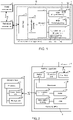
- Fig. 1 is a diagram showing an information processing system according to an embodiment, and is, in particular, a block diagram schematically showing a configuration example of an IC card 1.
- the information processing system has the IC card (electronic apparatus) 1, a terminal apparatus (IC card processing apparatus) 2, and a host apparatus 3.
- the IC card communicates with the terminal apparatus 2, and the terminal apparatus 2 communicates with the host apparatus 3.
- the host apparatus 3 is connected to, for example, the terminal apparatus 2 via a network.
- the host apparatus 3 is an apparatus that transmits information such as a server on a network or a transmission source of a communication system.
- the host apparatus 3 outputs a patch program (described in detail later) for the IC card 1 to the terminal apparatus 2.
- the terminal apparatus 2 has a function of communicating with the host apparatus 3, and a function of communicating with the IC card 1.
- the terminal apparatus 2 supplies the patch program supplied from the host apparatus 3 to the IC card 1.
- the IC card 1 is communicatively connected to the terminal apparatus 2.
- the IC card 1 is an electronic apparatus having a function of communicating with the terminal apparatus 2 and a function of executing programs.
- the IC card 1 applies the patch program supplied from the host apparatus 3 via the terminal apparatus 2.
- the IC card 1 is a contact-type or a contactless-type IC card, which operates according to commands from the terminal apparatus 2, and the terminal apparatus 2 is an IC card processing apparatus (IC card reader/writer (R/W)).
- the IC card 1 may also be an electronic apparatus other than a contact-type or a contactless-type IC card
- the terminal apparatus 2 may also be any apparatus that can be communicatively connected to an interface of an electronic apparatus other than an IC card.
- the IC card 1 may also be a small electronic device mounted on the terminal apparatus 2.
- the host apparatus 3 is the transmission source of the patch program for the IC card 1 in the information processing system, and may be a personal computer (PC), a server, or a transmission apparatus of a broadcast communication system.
- the IC card 1 is a portable electronic device which is activated (becomes operational) by power supplied from the terminal apparatus 2.
- the IC card 1 operates according to a command from the terminal apparatus 2.
- the IC card 1 is also called a smart card.
- the IC card 1 is a contact-type IC card (contact IC card) or a contactless -type IC card (contactless IC card).
- the IC card 1 serving as the contact IC card is activated by being supplied with operating power and an operating clock from the terminal apparatus 2 via a contact unit serving as a communication interface.
- the IC card 1 serving as the contactless IC card is activated by receiving a radio wave from the terminal apparatus 2 via an antenna serving as the communication interface, a modulation/demodulation circuit, and the like, and generating operating power and an operating clock from the radio wave.
- the IC card 1 has a main body C.
- the main body C is made of a plastic or the like, and is formed to be card-shaped.
- the IC card 1 has a module M within the main body C.
- the module M one or more IC chips Ca and an external interface (interface) for communication are integrally formed in a connected state, and the module M is embedded in the main body C.
- the module M has a processor 11, a RAM 12, a ROM 13, a nonvolatile memory 14, a communication controller 15, an interface 16 and the like.
- the processor 11 includes a hardware circuit that performs various types of processing.
- the processor 11 may be a CPU (Central Processing Unit), for example.
- the processor 11 performs overall control of the IC card 1. In other words, the processor 11 is a controller.
- the processor 11 realizes various processing functions by executing programs stored in the ROM 13 or the nonvolatile memory 14. However, the various functions executed by the processor 11, which will be described later, may also be partly or entirely realized by a hardware circuit.
- the RAM 12 is a volatile memory that functions as a working memory.
- the RAM 12 also functions as a buffer that temporarily stores data and the like undergoing processing by the processor 11.
- the RAM 12 is provided with a communication buffer (transmit/receive buffer) that temporarily stores data to be transmitted to and data received from the terminal apparatus 2 via the communication controller 15 and the interface 16.
- the communication buffer provided in the RAM 12 is constituted by a transmit buffer that stores data to be transmitted and a receive buffer that stores received data.
- the RAM 12 also stores various types of control information for defining the communication buffer.
- the RAM 12 has a storage region 12a for storing a session key used for a secure messaging, which will be described later.
- the ROM 13 is a nonvolatile memory that functions as a program memory. Control programs, control data, and the like are preliminarily stored in the ROM 13.
- the ROM 13 is incorporated into the IC card 1 at the manufacturing stage in a state in which the control programs, the control data, and the like are stored therein. In other words, the control programs and the control data stored in the ROM 13 are preliminarily incorporated in accordance with the specifications of the IC card 1.
- the ROM 13 stores a program for the processor 11 to execute processing corresponding to a command received from the terminal apparatus 2.
- the ROM 13 has a storage region 13a for storing a program (a first program) to which a patch program, which will be described later, is applied.
- the nonvolatile memory 14 is a nonvolatile memory to which data can be written and rewritten.
- the nonvolatile memory 14 is configured by, for example, an EEPROM (registered trademark) (Electrically Erasable Programmable Read Only Memory), a flash ROM, or the like. Programs corresponding to the application of the IC card 1 and various types of data are written to the nonvolatile memory 14.
- the nonvolatile memory 14 is tamper-resistant, and data can be securely stored therein.
- program files, data files, or the like are defined, and control programs and various types of setting data are written into those files.
- the nonvolatile memory 14 stores various setting data for communication control, user data, application programs, and the like.
- the nonvolatile memory 14 has a section management table 14a, which will be described later.
- the nonvolatile memory 14 may also be provided with a storage region 14b for storing a fixed key that is used in secure messaging.
- the communication controller 15 is connected to the interface 16.
- the interface 16 is an interface for communicatively connecting to the external apparatus.
- the communication controller 15 and the interface 16 constitute a communication unit.
- the communication controller 15 and the interface 16 realize a communication function that uses a communication method corresponding to an interface of the terminal apparatus 2.
- the communication controller 15 and the interface 16 may also be configured to support a plurality of communication methods (e.g., contact communication and contactless communication).
- the communication controller 15 and the interface 16 constitute a communication unit that communicates with the terminal apparatus 2 through contact therewith.
- the interface 16 is constituted by a contact unit that can be brought into physical and electrical contact with a contact unit of the terminal apparatus 2
- the communication controller 15 is constituted by a circuit or the like that controls transmission and reception of signals via the contact unit.
- the communication controller 15 and the interface 16 constitute a communication unit that communicates with a card reader/writer of the terminal apparatus 2 in a contactless (wireless) manner.
- the interface 16 is constituted by an antenna that transmits and receives radio waves
- the communication controller 15 is constituted by a modulation circuit for generating a radio wave to be transmitted, a demodulation circuit for generating a signal from a received radio wave, and the like.
- Fig. 2 is a block diagram schematically showing a configuration example of an information processing system according to the embodiment.
- the terminal apparatus 2 of the information processing system is an IC card processing apparatus having a function of communicating with the IC card 1 via the card reader/writer, and a function of communicating with the host apparatus 3.
- the terminal apparatus 2 has a controller 21, a display unit 22, an operation unit 23, a card reader/writer 24, and the like.
- the controller 21 controls the overall operation of the terminal apparatus 2.
- the controller 21 includes a hardware circuit that performs various types of processing.
- the controller 21 is constituted by a processor (CPU) 25, a RAM 26, a ROM 27, a nonvolatile memory 28, a communication unit 29, and the like.
- the controller 21 is constituted by a personal computer (PC).
- the processor 25 executes various types of processing by executing programs stored in the ROM 27 or the nonvolatile memory 28.
- the RAM 26 functions as a working memory that temporarily stores data.
- the ROM 27 is a nonvolatile memory that stores programs, control data, and the like.
- the nonvolatile memory 28 is a rewritable nonvolatile memory.
- the communication unit 29 is an interface for communicating with the host apparatus 3.
- the controller 21 has a function of transmitting commands to the IC card 1 using the card reader/writer 24, a function of performing various types of processing based on data received from the IC card 1, and other functions. For example, the controller 21 performs control for writing data to nonvolatile memories in the IC card 1 by transmitting a data write command to the IC card 1 via the card reader/writer 24. Also, the controller 21 performs control to read data from the IC card 1 by transmitting a read command to the IC card 1. Also, the controller 21 has a function of executing a plurality of applications.
- the display unit 22 is a display apparatus that displays various types of information under the control of the controller 21.
- the operating unit 23 is constituted by a keyboard, a numeric keypad, a pointing device, and the like.
- the operating unit 23 is a unit for allowing an operator of the terminal apparatus 2 to input various operating instructions, data, and the like.
- the operating unit 23 also functions as an input unit for inputting identification information of a user of the IC card 1 or authentication information such as a password.
- the card reader/writer 24 is an interface apparatus for communicating with the IC card 1.
- the card reader/writer 24 is configured by an interface corresponding to the communication method of the IC card 1.
- the card reader/writer 24 is constituted by a contact unit for physically and electrically connecting to the contact unit of the IC card 1, and the like.
- the card reader/writer 24 is constituted by an antenna for performing wireless communication with the IC card 1, a communication controller, and the like.
- the card reader/writer 24 supplies power and a clock signal to the IC card 1, performs reset control of the IC card 1, and transmits and receives data to and from the IC card 1. Based on the control by the controller 21, the card reader/writer 24 activates (starts up) the IC card 1, transmits various commands, receives responses to the transmitted commands, and so on.
- the host apparatus 3 is an apparatus that is communicatively connected to the terminal apparatus 2.
- the host apparatus 3 is a server connected to a communication unit 29 of the terminal apparatus 2 via a network.
- the communication unit 29 includes an interface.
- the host apparatus 3 may also be a personal computer (PC) or the like connected to the terminal apparatus 2.
- PC personal computer
- the host apparatus 3 has a processor (CPU) 31, a storage unit 32, and a communication unit 33, and the like.
- the processor 31 executes various processing as the host apparatus 3 by executing programs stored in the storage unit 32.
- the storage unit 32 has a RAM, a ROM, a rewritable nonvolatile memory, and the like.
- the storage unit 32 stores, for example, a patch program to be applied to the IC card 1.
- the communication unit 33 is an interface for communicating with the terminal apparatus 2.
- the processor 31 of the host apparatus 3 performs processing for transmitting the patch program, stored in the storage unit 32, that is to be applied to the IC card 1 to the terminal apparatus 2.
- Fig. 3 is a diagram showing a configuration example of a region to which the patch programs are written in the nonvolatile memory 14 of the IC card 1 according to the embodiment.
- the nonvolatile memory 14 stores a section management table 14a, and a plurality of section regions (pieces of section information) 40 (401, ..., 40n).
- the section management table 14a stores information for managing each pieces of section information.
- the section regions 40 store patch programs.
- Each section regions 40 (401, ..., 40n) has a table region 41 (411, ..., 41n) and a program region 42 (421, ..., 42n).
- the patch programs stored in the section regions 40 are programs to be applied to a program which is preliminarily installed in the ROM 13 or the nonvolatile memory 14.
- the patch programs are, for example, programs for fixing bugs in a program stored in the ROM 13 or nonvolatile memory 14.
- the program which is preliminarily stored in the ROM 13 or the nonvolatile memory 14 is configured to apply the patch programs as required, with reference to the information stored in the section management table 14a. For example, information indicating a patch program to be applied (for example, an identification number of the patch program) is set, and the program which is preliminarily stored in the ROM 13 or the nonvolatile memory 14 operates so as to apply the patch program according to that information.
- the section management table 14a stores information for managing the patch programs divided among the plurality of section regions (pieces of section information) 40 (401, ..., 40n).
- the section management table 14a has n section regions 40 (401, ...40n) for managing the n patch programs.
- the table region 41 of each section region 40 stores a number for identifying the patch program (patch number), and an address and a size of data (program) that is managed in the section.
- the program region 42 of each section region 40 stores the body of the patch program that is managed in the section.
- the nonvolatile memory 14 may also be provided with a region 14b for storing key information for secure messaging.
- the region 14b stores information indicating a fixed key for secure messaging.
- the fixed key for secure messaging has an encryption key and an authenticator key.
- the encryption key is used to encrypt a data section of a command.
- the authenticator key is used to generate an authenticator for a message.
- the pieces of key information stored in the region 14b may also be configured to be changed by using a dedicated command.
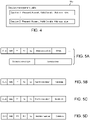
- Fig. 4 is a diagram for illustrating management information of each section in the section management table 14a.
- the section management table 14a stores, as information related to each section, information indicating the presence or absence of data (patch program) (Present/Absent), information indicating the validity of the data (Valid/Invalid), information indicating an address of the section region, and information indicating a size of the section region.
- the information indicating the presence or absence of data and the information indicating the validity of data are information indicating the validity/invalidity of the section. In the case where the information indicating the presence or absence of the data indicates "present” and the information indicating the validity of data indicates "Valid", the section is shown to be valid.
- the management information managed by the section management table 14a can be rewritten by commands from the terminal apparatus 2.
- the management information of the section is added to the section management table 14a.
- the section management table 14a is updated in the case where the state of the section regions is changed.
- the section regions are validated by a section validation command, invalidated by a section invalidation command, and deleted by a section deletion command.
- Figs. 5A to 5D are diagrams showing configuration examples of each type of command for controlling the section information in the section management table 14a.
- Fig. 5A is a diagram showing a configuration example of a section data write command.
- Fig. 5B is a diagram showing a configuration example of the section validation command.
- Fig. 5C is a diagram showing a configuration example of a section invalidation command.
- Fig. 5D is a diagram showing a configuration example of a section deletion command.
- the commands shown in Figs. 5A to 5D are each constituted by CLA, INS, P1, P2, Lc, and a data section.
- the section data write command shown in Fig. 5A is a command for requesting writing of a patch program.
- the IC card 1 Upon receiving the section data write command, the IC card 1 sets the designated section information in the section management table 14a to "Present".
- "Section number”, “Offset”, “Section data (write data) length”, and “Section data” are stored in the stated order in the data section.
- “Section number” is information indicating the section to be written.
- “Offset” is information indicating the write start position.
- “Section data length” is information indicating the length of data to be written by the command.
- “Section data” is information indicating the data to be written by the command.
- the section data write command requests processing for writing "Section data” of an amount of “Section data length” from the position of "Offset” in the section region which is designated to be written by the "Section number".
- the section data may also be data obtained by dividing the patch program as data to be written to the section region, or data for collectively transmitting the entire patch program.
- the section validation command shown in Fig. 5B is a command for instructing to validate the designated section.
- the processor 11 of the IC card 1 sets the management information of the section designated by the command in the section management table 14a to "Valid".
- "Section number” and "Validate” are stored in the stated order in the data section.
- "Section number” is information indicating the section to be subjected to validation processing.
- "Validate” is information instructing to validate the section.
- the section invalidation command shown in Fig. 5C is a command for instructing to invalidate the designated section.
- the processor 11 of the IC card 1 sets the management information of the section designated by the command in the section management table 14a to "Invalid".
- "Section number” and “Invalidate” are stored in the stated order in the data section.
- “Section number” is information indicating the section to be subjected to invalidation processing.
- “Invalidate” is information instructing to invalidate the section.
- the section deletion command shown in Fig. 5D is a command for instructing to delete the designated section.
- the processor 11 of the IC card 1 sets the management information of the section designated by the command in the section management table 14a to "None".
- "Section number” and "Delete” are stored in the stated order in the data section.
- "Section number” is information indicating the section to be subjected to deletion processing.
- “Deletion” is information instructing to delete the section.
- Each of the commands shown in Figs. 5A to 5D may also be configured so as to be transmitted and received as a secure messaging command.
- the secure messaging command is generated as a command in which the message (the data section of the command) is encrypted with an encryption key and to which an authenticator for the message is added.
- the key for secure messaging may be a session key to be exchanged in mutual authentication, or a fixed key such as shown in Fig. 3 .
- Fig. 6 is a diagram showing an example of the session key for secure messaging stored in the RAM 12 of the IC card 1.
- the session key for secure messaging includes an encryption key and an authenticator key.
- the encryption key is used to encrypt or decrypt the data section of the command.
- the authenticator key is used to generate an authenticator for a message. Since these session keys are generated or exchanged every session by a dedicated command from the terminal apparatus 2 to the IC card 1, the session keys are rewritten each time.
- the session keys are stored in the RAM 12 of the IC card 1 and in the RAM 26 of the terminal apparatus 2, and used for secure messaging between the IC card 1 and the terminal apparatus 2.
- Fig. 7 is a diagram showing an example of a command which has been converted for secure messaging (secure messaging command).
- the secure messaging command has an encrypted data section and an authenticator.
- the key used for secure messaging may be the above-mentioned session key, or a fixed key such as shown in Fig. 3 .
- the commands shown in Figs. 5A to 5D become a secure messaging command such as shown in Fig. 7 .
- a secure messaging command such as shown in Fig. 7
- the contents of the data section cannot be known from outside due to the encryption, and tampering of the data can be detected by the authenticator.
- the IC card 1 and the terminal apparatus 2 perform mutual authentication to establish the access condition.
- the IC card 1 and the terminal apparatus 2 exchange session keys in the mutual authentication. Using this session key, the terminal apparatus 2 performs encryption of the message (the data in the data section) for each command and adds the authenticator to the message to generate a secure messaging command.
- the IC card 1 interprets the secure messaging command from the terminal apparatus 2 with the session key.
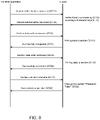
- Fig. 8 shows a sequence for illustrating the flow of processing for writing a patch program (patch application processing) from the terminal apparatus 2 by the IC card 1 according to the embodiment.
- Fig. 8 shows commands and responses that are transmitted and received between the IC card 1 and the terminal apparatus (IC card processing apparatus) 2 in the patch application processing.
- the terminal apparatus 2 and the IC card 1 perform mutual authentication and exchange session keys (ST11 to ST14). That is, the processor 25 of the terminal apparatus 2 sends a mutual authentication command to the IC card 1 (ST11), and starts the mutual authentication. Upon receiving the mutual authentication command, the processor 11 of the IC card 1 executes mutual authentication with the terminal apparatus 2 corresponding to the mutual authentication command (ST12). In this mutual authentication, the IC card 1 and the terminal apparatus 2 exchange the session keys to be used for secure messaging (ST13). When the mutual authentication is completed, the processor 11 of the IC card 1 transmits a response to the mutual authentication command to the terminal apparatus 2 (ST14). Here, it is assumed that the mutual authentication was successful and that the processor 11 of the IC card 1 transmits a response indicating that authentication was successful to the terminal apparatus 2.
- the operation example shown in Fig. 8 shows the terminal apparatus 2 and the IC card 1 performing mutual authentication and exchanging session keys
- the IC card 1 and the terminal apparatus 2 may also perform secure messaging by using a fixed key instead of the session keys.
- the terminal apparatus 2 and the IC card 1 execute write processing for writing a patch program to the IC card 1 (ST15 to ST20).
- the patch program is supplied from the host apparatus 3 to the terminal apparatus 2.
- the terminal apparatus 2 may write the patch program to the IC card 1 with a plurality of write commands, or may write the patch program with one write command.
- the terminal apparatus 2 may also determine the number of write commands to supply to the IC card 1 according to on the length (size) of the patch program.
- Fig. 8 an operation example in which writing of a patch program to a section region is completed with two write commands is shown.
- the processor 25 of the terminal apparatus 2 when the mutual authentication is completed, the processor 25 of the terminal apparatus 2 generates a section data write command for applying the patch program supplied from the host apparatus 3 to the IC card 1.
- the patch program from the host apparatus 3 is written to the IC card 1 with two write commands (first and second section data write commands).
- the processor 25 of the terminal apparatus 2 generates the first section data write command and the second section data write command for the patch program to be applied to the IC card 1.
- the processor 25 of the terminal apparatus 2 transmits the generated first section data write command to the IC card 1 (ST15).
- the processor 11 of the IC card 1 adds a section region to be managed by the section management table 14a, and writes information corresponding to the received command into the added section region (ST16).
- a section number is assumed to be set for each section in the chronological order.
- the processor 11 upon receiving the first section data write command, the processor 11 adds a section region 40 to which a new section number obtained by incrementing (+1) the last (latest) section number managed by the current section management table 14a is added.
- the processor 11 Upon adding the new section region 40, the processor 11 writes information such as the patch number, the starting address, and the like, to the table region 41 of the added section region 40, and writes the program body to be stored in the data section of the command to the program region 42.
- the processor 11 decrypts the data section of the command by using the encryption key of the session key or the encryption key of the fixed key, and checks the validity of the command with the authenticator by using the authentication key.
- the processor 11 performs write processing such as described above, based on the data obtained by decrypting the data section of the command whose validity has been checked.
- the processor 11 Upon completing the write processing corresponding to the first section data write command, the processor 11 transmits a response indicating that writing corresponding to the command was successfully completed to the terminal apparatus 2 (ST17). In this response, the section number indicating the section to which the data has been written (the added section) and the like is also notified.
- the processor 25 of the terminal apparatus 2 Upon receiving the response indicating successful completion with respect to the first section data write command from the IC card 1, the processor 25 of the terminal apparatus 2 transmits the second section data write command to the IC card 1 (ST18).
- the processor 11 of the IC card 1 Upon receiving the second section data write command, the processor 11 of the IC card 1 writes information corresponding to the received command to the section added in response to the first section data write command in ST16 (ST19). For example, the processor 11 adds program data stored in the data section of the second section data write command to the program region 42 of the added section region 40. Upon completing the write processing corresponding to the second section data write command, the processor 11 transmits a response indicating that writing of data to the section was successfully completed to the terminal apparatus 2 (ST20).
- the processor 25 of the terminal apparatus 2 determines writing of the patch program as section data has been completed.
- the terminal apparatus 2 and the IC card 1 Upon the completion of writing the patch program, the terminal apparatus 2 and the IC card 1 perform processing for validating the section to which the patch program has been written by the first and second section data write command (ST21 to ST23).
- the processor 25 of the terminal apparatus 2 transmits a section validation command for validating the section to which the patch program has been written by the first and second section data write command (ST21). For example, the processor 25 generates the section validation command, by setting the section number indicating the section to which the data has been written in the section validation command as shown in Fig. 5B .
- the processor 11 of the IC card 1 validates the section having the section number designated by the section validation command (ST22). For example, the processor 11 writes information indicating that data is present ("Present") and information indicating that the data is valid ("Valid"), as the management information of the section having the section number designated by the section validation command in the section management table 14a. Thus, in the IC card 1, the section storing the patch program is validated. Upon validating the designated section, the processor 11 transmits a response indicating that validation of the section was successfully completed to the terminal apparatus 2 (ST23).
- the processor 11 of the terminal apparatus 2 adds information indicating that the last data of the patch program (that is, the last data to be written to the section) is included (or information indicating that writing of the patch program has ended) to the second section data write command.
- the processor 11 of the IC card 1 can determine that writing of data to the section has ended. Based on this determination, the processor 11 may update the management information of that section in the section management table 14a to show that the data is "Present" and "Valid".
- the terminal apparatus 2 may designate the length of a patch program whose writing is requested with a plurality (two) of the write commands (the size of the data to be written to the program region 42) in the first section data write command.
- the IC card 1 may also determine that writing of data to the section added in response to the plurality of commands has ended, when the length of data written to the program region 42 of that section has reached the designated length of the patch program.
- each section managed by the section management table should be either in the state before writing a patch program or in the state after writing a patch program.
- the management information of each section managed by the section management table the information indicating the presence or absence ("present” or “absent") of data (patch program) and information indicating the validity of data ("Valid” or "Invalid") are updated in the patch application processing.
- the state before writing is "Absent” and "Invalid”
- the state after writing is "Present” and "Valid”.
- the management information is controlled to be in the state before writing ("Absent” and "Invalid"), not to be in an irregular state such as "Absent” and "Valid", for example.
- the management information of that section managed by the section management table may be in the state "Present” and "Invalid".
- Fig. 9 is a diagram schematically showing an operation for executing a patch program (patch processing) in the IC card 1.
- the example shown in Fig. 9 shows an operation for executing a patch program on a program (the first program) stored in the ROM 13 during the execution of the program.
- the processor 11 searches for a valid section, and further search for a patch program to be applied to the program corresponding to that section, with reference to the section management table 14a provided in the nonvolatile memory 14.
- the section management table 14a manages a plurality of sections having section numbers 1 to n (n is natural number).
- the processor 11 starts searching from the section with the largest section number in the section management table 14a.
- the new patch program is always stored in the added section (the section with the largest section number).
- the processor 11 searches each section for a valid section in order from the section with the largest section number (the latest section) to the section with the smallest section number (the oldest section).
- the processor 11 checks the section with the next smallest section number. That is to say, if a patch program corresponding to the program being executed is not found, the processor 11 searches the section with the next smallest section number. If a patch program corresponding to the program being executed is ultimately not found even after checking the section with the section number 1, the processor 11 determines that there is no patch program to be applied. If a patch program corresponding to the program being executed is found, the processor 11 executes the patch program stored in the program region of the section.
- Fig. 10 is a flowchart for illustrating an operation example of the patch processing in the IC card 1.
- the processor 11 of the IC card 1 determines if patch processing on the program (first program) stored in the ROM 13 or the nonvolatile memory 14 is required or not during execution of the program. For example, the processor 11 determines to start the patch processing by processing that is called from the location that requires patch processing set in the program being executed.
- the patch program applied to the program is identified by a patch number.
- the patch number may be obtained, for example, by using the INS of the command supplied to the IC card 1 from the terminal apparatus 2. It is also possible to set a number of an entry point in the program and obtain the entry point number as the patch number.
- the processor 11 obtains a number for identifying the patch program (called the patch number) to be applied to the program being executed (first program) (ST31).
- the processor 11 obtains the entry point number set in the program being executed as the patch number.
- the processor 11 searches for the section storing the patch program to be executed, with reference to the section management table 14a.
- the processor 11 Upon starting the search for the patch program, the processor 11 searches for a section in which the patch program is valid (i.e., valid section) in the section management table 14a, in descending order from the section with the largest section number. For example, the processor 11 checks whether data is present ("Present") and the data is valid ("Valid”) or not in the table region of each section, in descending order from the section with the largest section number, and determines whether the section is valid or not.
- a section in which the patch program is valid i.e., valid section
- the processor 11 checks whether data is present ("Present") and the data is valid ("Valid") or not in the table region of each section, in descending order from the section with the largest section number, and determines whether the section is valid or not.
- the processor 11 terminates the patch processing on the program being executed.
- the processor 11 In the case where the processor 11 detects a section in which data is "Present” and "Valid” (ST33, YES), the processor 11 obtains an address indicating the corresponding section region (section information) 40 from the corresponding section management information in the section management table 14a (ST34).
- the processor 11 When the processor 11 obtains the address of the section region 40, the processor 11 accesses the section region 40 according to the obtained address, and specifies the patch number stored in the table region 41 of the section region 40 (ST35). When the processor 11 specifies the stored patch number stored in the table region 41, the processor 11 determines whether the patch number stored in the table region 41 matches the patch number of the patch program to be applied to the program being executed (ST36).
- the processor 11 executes the patch program stored in the program region 42 of that section region 40 (ST38), and terminates the patch processing.
- the processor 11 searches for a section in which the patch program is valid, in order from the section with the section number which is smaller than the section number of the section which has been checked (ST37). Then, the processor 11 returns from ST37 to ST33, and performs the above processing based on the result of the search processing in ST37.
- the region storing the patch program to be applied to a program which is preliminarily installed in the ROM or the nonvolatile memory is a section consisting of a table region and a program region, and each section is managed based on the management information of the management table.
- the IC card according to the embodiment searches for the patch program to be applied to the program being executed with reference to the management information of the management table, and executes the found patch program.
- the IC card according to the present embodiment can reliably apply patch programs to software programs including the OS during operation, rather than downloading and adding applications. That is, in the IC card according to the present embodiment, patch programs that aim to fix bugs and the like can be reliably applied to preliminarily installed programs including the OS.
- the IC card according to the present embodiment validates each section based on the management information in the management table after storage of a patch program in the section has been completed. Thereby, in the IC card according to the present embodiment, patch programs that are added are applied in order so as to update each program.
- the IC card even if a disturbance such as power interruption occurs during write processing of a patch program (patch application), it is possible to treat section data (patch program) with respect to which write processing has not been completed as invalid data. Accordingly, the IC card prevents patch processing (operation) using incomplete data (patch program) from being performed, and can return to the state before writing where operation was being reliably performed.
- an electronic apparatus an IC card, and an information processing system that are capable of reliably applying a patch program to a program.
Landscapes
- Engineering & Computer Science (AREA)
- Theoretical Computer Science (AREA)
- General Engineering & Computer Science (AREA)
- Computer Security & Cryptography (AREA)
- Software Systems (AREA)
- General Physics & Mathematics (AREA)
- Physics & Mathematics (AREA)
- Computer Hardware Design (AREA)
- Data Mining & Analysis (AREA)
- Databases & Information Systems (AREA)
- Stored Programmes (AREA)
- Computer And Data Communications (AREA)
- Information Transfer Between Computers (AREA)
Claims (9)
- Elektronische Vorrichtung, umfassend:eine Kommunikationseinheit (15, 16), die eingerichtet ist, um mit einer Endeinrichtung (2) zu kommunizieren;eine erste Speichereinheit (13), die eingerichtet ist, um ein erstes Programm zu speichern;eine zweite Speichereinheit (14), die eingerichtet ist, um für jeden Abschnitt ein Patch-Programm für das erste Programm zu speichern, wobei das Patch-Programm von der Endeinrichtung (2) über die Kommunikationseinheit (15, 16) empfangen wird; undeine Steuerung (11), die eingerichtet ist, um in einem Fall der Ausführung des ersten Programms ein letztes Patch-Programm, das in den Abschnitten in der zweiten Speichereinheit (14) gespeichert ist, anzuwenden, dadurch gekennzeichnet, dassdie zweite Speichereinheit (14) eingerichtet ist, um eine Abschnittsverwaltungstabelle (14a) zu speichern, die Informationen zum Verwalten jedes der Abschnitte speichert, einschließlich Informationen, die das Vorhandensein oder das Nichtvorhandensein des Patch-Programms und die Gültigkeit oder die Ungültigkeit des Patch-Programms für jeden der Abschnitte anzeigen, wobei die Informationen, die das Vorhandensein oder das Nichtvorhandensein des Patch-Programms und die Gültigkeit oder die Ungültigkeit des Patch-Programms anzeigen, jeweils durch einen Befehl von der Endeinrichtung (2) änderbar sind, unddie Steuerung (11) eingerichtet ist, um in der Abschnittsverwaltungstabelle (14a) einen geeigneten Abschnitt zu spezifizieren, der ein Patch-Programm speichert, dessen Vorhandensein und Gültigkeit als ein gültiges Patch-Programm angezeigt wird, das auf das erste Programm anzuwenden ist.
- Elektronische Vorrichtung nach Anspruch 1,
wobei die Steuerung (11) beim Empfang eines neuen Patch-Programms über die Kommunikationseinheit (15, 16) einen neuen Abschnitt hinzufügt, der auf der Grundlage von Verwaltungsinformationen der Abschnittsverwaltungstabelle (14a) zu verwalten ist, und das empfangene neue Patch-Programm in dem hinzugefügten Abschnitt speichert. - Elektronische Vorrichtung nach einem der Ansprüche 1 bis 2,
wobei die Steuerung (11) die in der zweiten Speichereinheit (14) vorhandenen Abschnitte unter Bezugnahme auf die Verwaltungsinformationen der Abschnittsverwaltungstabelle (14a) in der Reihenfolge des zuletzt hinzugefügten Abschnitts nach einem Abschnitt durchsucht, der das Patch-Programm speichert, das auf das erste Programm anzuwenden ist. - Elektronische Vorrichtung nach einem der Ansprüche 1 bis 3,
wobei die Steuerung (11) ein Patch-Programm von der Endeinrichtung (2) empfängt, nachdem die Authentifizierung mit der Endeinrichtung (2) erfolgreich durchgeführt wurde. - Elektronische Vorrichtung nach einem der Ansprüche 1 bis 4, umfassend:ein Modul (M), das die Kommunikationseinheit (15, 16), die erste Speichereinheit (13), die zweite Speichereinheit (14) und die Steuerung (11) aufweist; undeinen Hauptkörper (C), in den das Modul (M) eingebettet ist.
- Elektronische Vorrichtung nach Anspruch 5,
wobei der Hauptkörper (C) kartenförmig ist. - Informationsverarbeitungssystem, umfassend eine Endeinrichtung (2) und eine elektronische Vorrichtung (1), wobeidie Endeinrichtung (2) umfasst:eine erste Kommunikationseinheit (24), die eingerichtet ist, um mit der elektronischen Vorrichtung (1) zu kommunizieren; undeine erste Steuerung (21), die eingerichtet ist, um ein Patch-Programm, das auf ein Programm in der elektronischen Vorrichtung (1) anzuwenden ist, über die erste Kommunikationseinheit (24) an die elektronische Vorrichtung (1) zu übertragen, undwobei die elektronische Vorrichtung (1) umfasst:eine zweite Kommunikationseinheit (15, 16), die eingerichtet ist, um mit der Endeinrichtung (2) zu kommunizieren;eine erste Speichereinheit (13), die eingerichtet ist, um ein erstes Programm zu speichern, auf das das von der Endeinrichtung (2) übertragene Patch-Programm anzuwenden ist;eine zweite Speichereinheit (14), die eingerichtet ist, um für jeden Abschnitt das von der Endeinrichtung (2) über die zweite Kommunikationseinheit (15, 16) empfangene Patch-Programm zu speichern; undeine zweite Steuerung (11), die eingerichtet ist, um in einem Fall der Ausführung des ersten Programms ein letztes Patch-Programm, das in den Abschnitten in der zweiten Speichereinheit (14) gespeichert ist, anzuwenden, dadurch gekennzeichnet, dassdie zweite Speichereinheit (14) eingerichtet ist, um eine Abschnittsverwaltungstabelle (14a) zu speichern, die Informationen zum Verwalten jedes der Abschnitte speichert, einschließlich Informationen, die das Vorhandensein oder das Nichtvorhandensein des Patch-Programms und die Gültigkeit oder die Ungültigkeit des Patch-Programms für jeden der Abschnitte anzeigen, wobei die Informationen, die das Vorhandensein oder das Nichtvorhandensein des Patch-Programms und die Gültigkeit oder die Ungültigkeit des Patch-Programms anzeigen, jeweils durch einen Befehl von der Endeinrichtung (2) änderbar sind, unddie zweite Steuerung (11) eingerichtet ist, um in der Abschnittsverwaltungstabelle (14a) einen geeigneten Abschnitt zu spezifizieren, der ein Patch-Programm speichert, dessen Vorhandensein und Gültigkeit als ein gültiges Patch-Programm angezeigt sind, um auf das erste Programm anzuwenden zu sein.
- Informationsverarbeitungssystem nach Anspruch 7,
wobei die Endeinrichtung (2) weiterhin beinhaltet:eine dritte Kommunikationseinheit (29), die mit einer Host-Einrichtung (3) kommuniziert, undwobei die erste Steuerung (21) ein Patch-Programm, das auf ein Programm in der elektronischen Vorrichtung (1) anzuwenden ist, von der Host-Einrichtung (3) über die dritte Kommunikationseinheit (29) empfängt und das von der Host-Einrichtung (3) empfangene Patch-Programm über die erste Kommunikationseinheit (24) an die elektronische Vorrichtung (1) überträgt. - Informationsverarbeitungssystem nach Anspruch 7 oder 8,
wobei die elektronische Vorrichtung (1) nach einem der Ansprüche 1 bis 6 umgesetzt ist.
Applications Claiming Priority (1)
| Application Number | Priority Date | Filing Date | Title |
|---|---|---|---|
| JP2017003143A JP6845021B2 (ja) | 2017-01-12 | 2017-01-12 | 電子装置、icカードおよび情報処理システム |
Publications (3)
| Publication Number | Publication Date |
|---|---|
| EP3349112A2 EP3349112A2 (de) | 2018-07-18 |
| EP3349112A3 EP3349112A3 (de) | 2018-09-26 |
| EP3349112B1 true EP3349112B1 (de) | 2022-10-19 |
Family
ID=61007465
Family Applications (1)
| Application Number | Title | Priority Date | Filing Date |
|---|---|---|---|
| EP18151206.2A Active EP3349112B1 (de) | 2017-01-12 | 2018-01-11 | Elektronische vorrichtung und informationsverarbeitungssystem |
Country Status (3)
| Country | Link |
|---|---|
| US (1) | US10732955B2 (de) |
| EP (1) | EP3349112B1 (de) |
| JP (1) | JP6845021B2 (de) |
Families Citing this family (1)
| Publication number | Priority date | Publication date | Assignee | Title |
|---|---|---|---|---|
| US12393352B2 (en) * | 2021-10-22 | 2025-08-19 | Micron Technology, Inc. | Authenticated modification of memory system data |
Citations (1)
| Publication number | Priority date | Publication date | Assignee | Title |
|---|---|---|---|---|
| US20100180104A1 (en) * | 2009-01-15 | 2010-07-15 | Via Technologies, Inc. | Apparatus and method for patching microcode in a microprocessor using private ram of the microprocessor |
Family Cites Families (28)
| Publication number | Priority date | Publication date | Assignee | Title |
|---|---|---|---|---|
| JPH0644078A (ja) | 1992-07-27 | 1994-02-18 | Fujitsu Ltd | オンライン動作中のファームウェア変更方式 |
| JP2500771B2 (ja) | 1993-06-28 | 1996-05-29 | 日本電気株式会社 | ソフトウェア修正方式 |
| JP2984649B1 (ja) * | 1998-05-14 | 1999-11-29 | 埼玉日本電気株式会社 | メモリの読み出し制御方法およびプログラムの読み出し制御方法 |
| JP3990833B2 (ja) * | 1998-12-11 | 2007-10-17 | キヤノン株式会社 | 通信制御方法及び装置 |
| EP1150213B1 (de) * | 2000-04-28 | 2012-01-25 | TELEFONAKTIEBOLAGET LM ERICSSON (publ) | Datenverarbeitungssystem und Verfahren |
| JP3899223B2 (ja) | 2000-08-07 | 2007-03-28 | Necトーキン株式会社 | Icカードおよびicカード搭載処理プログラムの変更・追加方法 |
| US6763517B2 (en) * | 2001-02-12 | 2004-07-13 | Sun Microsystems, Inc. | Automated analysis of kernel and user core files including searching, ranking, and recommending patch files |
| US6976126B2 (en) * | 2003-03-11 | 2005-12-13 | Arm Limited | Accessing data values in a cache |
| CA2465151A1 (en) * | 2003-04-16 | 2004-10-16 | Novadigm, Inc. | Method and system for patch management |
| US7596721B1 (en) * | 2004-01-09 | 2009-09-29 | Maxtor Corporation | Methods and structure for patching embedded firmware |
| US7552430B2 (en) * | 2004-08-31 | 2009-06-23 | Microsoft Corporation | Patch sequencing |
| JP4828816B2 (ja) * | 2004-10-25 | 2011-11-30 | 株式会社東芝 | メモリカード、半導体装置、及びメモリカードの制御方法 |
| US7937697B2 (en) * | 2005-05-19 | 2011-05-03 | International Business Machines Corporation | Method, system and computer program for distributing software patches |
| US20070106980A1 (en) * | 2005-10-11 | 2007-05-10 | Bea Systems, Inc. | Patch management system |
| US20070113064A1 (en) * | 2005-11-17 | 2007-05-17 | Longyin Wei | Method and system for secure code patching |
| JP4976021B2 (ja) * | 2006-02-10 | 2012-07-18 | 株式会社リコー | ダウンロードシステム、拠点サーバ及びプログラム |
| US7711902B2 (en) * | 2006-04-07 | 2010-05-04 | Broadcom Corporation | Area effective cache with pseudo associative memory |
| US20080022380A1 (en) * | 2006-05-25 | 2008-01-24 | Gemalto, Inc. | Method of patching applications on small resource-constrained secure devices |
| JP2008077458A (ja) * | 2006-09-22 | 2008-04-03 | Fujitsu Ltd | 記憶データ処理装置、記憶装置、記憶データ処理プログラム |
| SG146551A1 (en) * | 2007-03-29 | 2008-10-30 | Toshiba Kk | Portable electronic device and control method of portable electronic device |
| EP2003556A1 (de) * | 2007-05-25 | 2008-12-17 | Axalto SA | Verfahren zur Verarbeitung von Anwendungsbefehlen, die von physischen Kanälen ausgegeben wurden, mittels einer tragbaren elektronischen Vorrichtung sowie entsprechende Vorrichtung und entsprechendes System |
| FR2928754B1 (fr) * | 2008-03-13 | 2012-05-18 | Sagem Securite | Carte a circuit integre ayant un programme d'exploitation modifiable et procede de modification correspondant |
| US8468516B1 (en) * | 2008-12-19 | 2013-06-18 | Juniper Networks, Inc. | Creating hot patches for embedded systems |
| US8521944B2 (en) * | 2010-08-31 | 2013-08-27 | Intel Corporation | Performing memory accesses using memory context information |
| JP2012064048A (ja) | 2010-09-16 | 2012-03-29 | Toshiba Corp | 携帯可能電子装置、非接触icカード、および携帯可能電子装置のコマンド処理方法 |
| WO2014112969A1 (en) * | 2013-01-15 | 2014-07-24 | Hewlett-Packard Development Company, L.P. | Dynamic firmware updating |
| US9514041B2 (en) * | 2013-03-08 | 2016-12-06 | Kabushiki Kaisha Toshiba | Memory controller and memory system |
| JP2018160156A (ja) * | 2017-03-23 | 2018-10-11 | 東芝メモリ株式会社 | メモリシステム |
-
2017
- 2017-01-12 JP JP2017003143A patent/JP6845021B2/ja active Active
-
2018
- 2018-01-11 US US15/867,837 patent/US10732955B2/en active Active
- 2018-01-11 EP EP18151206.2A patent/EP3349112B1/de active Active
Patent Citations (1)
| Publication number | Priority date | Publication date | Assignee | Title |
|---|---|---|---|---|
| US20100180104A1 (en) * | 2009-01-15 | 2010-07-15 | Via Technologies, Inc. | Apparatus and method for patching microcode in a microprocessor using private ram of the microprocessor |
Also Published As
| Publication number | Publication date |
|---|---|
| EP3349112A2 (de) | 2018-07-18 |
| JP6845021B2 (ja) | 2021-03-17 |
| JP2018112913A (ja) | 2018-07-19 |
| US20180196661A1 (en) | 2018-07-12 |
| EP3349112A3 (de) | 2018-09-26 |
| US10732955B2 (en) | 2020-08-04 |
Similar Documents
| Publication | Publication Date | Title |
|---|---|---|
| US9183400B2 (en) | IC card and IC card control method | |
| US20060086785A1 (en) | Portable electronic apparatus and method of updating application in portable electronic apparatus | |
| JP6426411B2 (ja) | Icカード及び携帯可能電子装置 | |
| EP3349112B1 (de) | Elektronische vorrichtung und informationsverarbeitungssystem | |
| KR101783526B1 (ko) | Ic 카드, 전자 장치 및 휴대 가능 전자 장치 | |
| JP2018005561A (ja) | Icカード、携帯可能電子装置、および、icカード処理装置 | |
| JP5459845B2 (ja) | 携帯可能電子装置、携帯可能電子装置の制御方法及びicカード | |
| JP2010211516A (ja) | 携帯可能電子装置および携帯可能電子装置におけるアクセス制御方法 | |
| JP6370669B2 (ja) | Icカード、携帯可能電子装置、及び、icカード処理装置 | |
| JP4765608B2 (ja) | データ処理装置、データ処理プログラム、およびデータ処理システム | |
| JP2014059806A (ja) | Icカード、携帯可能電子装置、及びicカード処理装置 | |
| JP2016081117A (ja) | Icカード、携帯可能電子装置、及び、icカード製造方法 | |
| JP7556100B1 (ja) | 携帯可能電子装置、icカードおよびicカード処理装置 | |
| JP2014182649A (ja) | Icカード、携帯可能電子装置、icカード処理装置及びicカード処理システム | |
| JP6178387B2 (ja) | 電子装置、及び電子装置の制御方法 | |
| JP5306151B2 (ja) | 携帯可能電子装置 | |
| JP2023139488A (ja) | Icカード、携帯可能電子装置およびicカード処理システム | |
| JP2016129072A (ja) | Icカード、携帯可能電子装置、及びicカード処理装置 | |
| JP2016177850A (ja) | Icカード、携帯可能電子装置、及びicカード処理装置 | |
| JP2014160499A (ja) | 携帯可能電子装置、及び携帯可能電子装置の制御方法 | |
| JP2014063302A (ja) | Icカード、および携帯可能電子装置 | |
| JP2013196346A (ja) | Icカード、携帯可能電子装置及びicカードのコマンド処理方法 | |
| JP2018152142A (ja) | Icカード、携帯可能電子装置、及び、icカード処理装置 | |
| JP2016027505A (ja) | Icカード、携帯可能電子装置及びicカードの制御方法 | |
| JP2016206975A (ja) | Icカード、携帯可能電子装置、icカード処理装置、及び、icカード処理システム |
Legal Events
| Date | Code | Title | Description |
|---|---|---|---|
| PUAI | Public reference made under article 153(3) epc to a published international application that has entered the european phase |
Free format text: ORIGINAL CODE: 0009012 |
|
| STAA | Information on the status of an ep patent application or granted ep patent |
Free format text: STATUS: REQUEST FOR EXAMINATION WAS MADE |
|
| 17P | Request for examination filed |
Effective date: 20180116 |
|
| AK | Designated contracting states |
Kind code of ref document: A2 Designated state(s): AL AT BE BG CH CY CZ DE DK EE ES FI FR GB GR HR HU IE IS IT LI LT LU LV MC MK MT NL NO PL PT RO RS SE SI SK SM TR |
|
| AX | Request for extension of the european patent |
Extension state: BA ME |
|
| PUAL | Search report despatched |
Free format text: ORIGINAL CODE: 0009013 |
|
| AK | Designated contracting states |
Kind code of ref document: A3 Designated state(s): AL AT BE BG CH CY CZ DE DK EE ES FI FR GB GR HR HU IE IS IT LI LT LU LV MC MK MT NL NO PL PT RO RS SE SI SK SM TR |
|
| AX | Request for extension of the european patent |
Extension state: BA ME |
|
| RIC1 | Information provided on ipc code assigned before grant |
Ipc: G06F 8/65 20180101AFI20180820BHEP Ipc: G06F 8/654 20180101ALI20180820BHEP |
|
| STAA | Information on the status of an ep patent application or granted ep patent |
Free format text: STATUS: EXAMINATION IS IN PROGRESS |
|
| 17Q | First examination report despatched |
Effective date: 20210219 |
|
| RIC1 | Information provided on ipc code assigned before grant |
Ipc: G06F 21/44 20130101ALI20220504BHEP Ipc: G06F 8/654 20180101ALI20220504BHEP Ipc: G06F 8/65 20180101AFI20220504BHEP |
|
| GRAP | Despatch of communication of intention to grant a patent |
Free format text: ORIGINAL CODE: EPIDOSNIGR1 |
|
| STAA | Information on the status of an ep patent application or granted ep patent |
Free format text: STATUS: GRANT OF PATENT IS INTENDED |
|
| INTG | Intention to grant announced |
Effective date: 20220610 |
|
| GRAS | Grant fee paid |
Free format text: ORIGINAL CODE: EPIDOSNIGR3 |
|
| GRAA | (expected) grant |
Free format text: ORIGINAL CODE: 0009210 |
|
| STAA | Information on the status of an ep patent application or granted ep patent |
Free format text: STATUS: THE PATENT HAS BEEN GRANTED |
|
| AK | Designated contracting states |
Kind code of ref document: B1 Designated state(s): AL AT BE BG CH CY CZ DE DK EE ES FI FR GB GR HR HU IE IS IT LI LT LU LV MC MK MT NL NO PL PT RO RS SE SI SK SM TR |
|
| REG | Reference to a national code |
Ref country code: GB Ref legal event code: FG4D |
|
| REG | Reference to a national code |
Ref country code: CH Ref legal event code: EP |
|
| REG | Reference to a national code |
Ref country code: IE Ref legal event code: FG4D |
|
| REG | Reference to a national code |
Ref country code: DE Ref legal event code: R096 Ref document number: 602018041864 Country of ref document: DE |
|
| REG | Reference to a national code |
Ref country code: AT Ref legal event code: REF Ref document number: 1525979 Country of ref document: AT Kind code of ref document: T Effective date: 20221115 |
|
| REG | Reference to a national code |
Ref country code: LT Ref legal event code: MG9D |
|
| REG | Reference to a national code |
Ref country code: NL Ref legal event code: MP Effective date: 20221019 |
|
| REG | Reference to a national code |
Ref country code: AT Ref legal event code: MK05 Ref document number: 1525979 Country of ref document: AT Kind code of ref document: T Effective date: 20221019 |
|
| PG25 | Lapsed in a contracting state [announced via postgrant information from national office to epo] |
Ref country code: NL Free format text: LAPSE BECAUSE OF FAILURE TO SUBMIT A TRANSLATION OF THE DESCRIPTION OR TO PAY THE FEE WITHIN THE PRESCRIBED TIME-LIMIT Effective date: 20221019 |
|
| PG25 | Lapsed in a contracting state [announced via postgrant information from national office to epo] |
Ref country code: SE Free format text: LAPSE BECAUSE OF FAILURE TO SUBMIT A TRANSLATION OF THE DESCRIPTION OR TO PAY THE FEE WITHIN THE PRESCRIBED TIME-LIMIT Effective date: 20221019 Ref country code: PT Free format text: LAPSE BECAUSE OF FAILURE TO SUBMIT A TRANSLATION OF THE DESCRIPTION OR TO PAY THE FEE WITHIN THE PRESCRIBED TIME-LIMIT Effective date: 20230220 Ref country code: NO Free format text: LAPSE BECAUSE OF FAILURE TO SUBMIT A TRANSLATION OF THE DESCRIPTION OR TO PAY THE FEE WITHIN THE PRESCRIBED TIME-LIMIT Effective date: 20230119 Ref country code: LT Free format text: LAPSE BECAUSE OF FAILURE TO SUBMIT A TRANSLATION OF THE DESCRIPTION OR TO PAY THE FEE WITHIN THE PRESCRIBED TIME-LIMIT Effective date: 20221019 Ref country code: FI Free format text: LAPSE BECAUSE OF FAILURE TO SUBMIT A TRANSLATION OF THE DESCRIPTION OR TO PAY THE FEE WITHIN THE PRESCRIBED TIME-LIMIT Effective date: 20221019 Ref country code: ES Free format text: LAPSE BECAUSE OF FAILURE TO SUBMIT A TRANSLATION OF THE DESCRIPTION OR TO PAY THE FEE WITHIN THE PRESCRIBED TIME-LIMIT Effective date: 20221019 Ref country code: AT Free format text: LAPSE BECAUSE OF FAILURE TO SUBMIT A TRANSLATION OF THE DESCRIPTION OR TO PAY THE FEE WITHIN THE PRESCRIBED TIME-LIMIT Effective date: 20221019 |
|
| PG25 | Lapsed in a contracting state [announced via postgrant information from national office to epo] |
Ref country code: RS Free format text: LAPSE BECAUSE OF FAILURE TO SUBMIT A TRANSLATION OF THE DESCRIPTION OR TO PAY THE FEE WITHIN THE PRESCRIBED TIME-LIMIT Effective date: 20221019 Ref country code: PL Free format text: LAPSE BECAUSE OF FAILURE TO SUBMIT A TRANSLATION OF THE DESCRIPTION OR TO PAY THE FEE WITHIN THE PRESCRIBED TIME-LIMIT Effective date: 20221019 Ref country code: LV Free format text: LAPSE BECAUSE OF FAILURE TO SUBMIT A TRANSLATION OF THE DESCRIPTION OR TO PAY THE FEE WITHIN THE PRESCRIBED TIME-LIMIT Effective date: 20221019 Ref country code: IS Free format text: LAPSE BECAUSE OF FAILURE TO SUBMIT A TRANSLATION OF THE DESCRIPTION OR TO PAY THE FEE WITHIN THE PRESCRIBED TIME-LIMIT Effective date: 20230219 Ref country code: HR Free format text: LAPSE BECAUSE OF FAILURE TO SUBMIT A TRANSLATION OF THE DESCRIPTION OR TO PAY THE FEE WITHIN THE PRESCRIBED TIME-LIMIT Effective date: 20221019 Ref country code: GR Free format text: LAPSE BECAUSE OF FAILURE TO SUBMIT A TRANSLATION OF THE DESCRIPTION OR TO PAY THE FEE WITHIN THE PRESCRIBED TIME-LIMIT Effective date: 20230120 |
|
| REG | Reference to a national code |
Ref country code: DE Ref legal event code: R097 Ref document number: 602018041864 Country of ref document: DE |
|
| PG25 | Lapsed in a contracting state [announced via postgrant information from national office to epo] |
Ref country code: SM Free format text: LAPSE BECAUSE OF FAILURE TO SUBMIT A TRANSLATION OF THE DESCRIPTION OR TO PAY THE FEE WITHIN THE PRESCRIBED TIME-LIMIT Effective date: 20221019 Ref country code: RO Free format text: LAPSE BECAUSE OF FAILURE TO SUBMIT A TRANSLATION OF THE DESCRIPTION OR TO PAY THE FEE WITHIN THE PRESCRIBED TIME-LIMIT Effective date: 20221019 Ref country code: EE Free format text: LAPSE BECAUSE OF FAILURE TO SUBMIT A TRANSLATION OF THE DESCRIPTION OR TO PAY THE FEE WITHIN THE PRESCRIBED TIME-LIMIT Effective date: 20221019 Ref country code: DK Free format text: LAPSE BECAUSE OF FAILURE TO SUBMIT A TRANSLATION OF THE DESCRIPTION OR TO PAY THE FEE WITHIN THE PRESCRIBED TIME-LIMIT Effective date: 20221019 Ref country code: CZ Free format text: LAPSE BECAUSE OF FAILURE TO SUBMIT A TRANSLATION OF THE DESCRIPTION OR TO PAY THE FEE WITHIN THE PRESCRIBED TIME-LIMIT Effective date: 20221019 |
|
| PLBE | No opposition filed within time limit |
Free format text: ORIGINAL CODE: 0009261 |
|
| STAA | Information on the status of an ep patent application or granted ep patent |
Free format text: STATUS: NO OPPOSITION FILED WITHIN TIME LIMIT |
|
| PG25 | Lapsed in a contracting state [announced via postgrant information from national office to epo] |
Ref country code: SK Free format text: LAPSE BECAUSE OF FAILURE TO SUBMIT A TRANSLATION OF THE DESCRIPTION OR TO PAY THE FEE WITHIN THE PRESCRIBED TIME-LIMIT Effective date: 20221019 Ref country code: AL Free format text: LAPSE BECAUSE OF FAILURE TO SUBMIT A TRANSLATION OF THE DESCRIPTION OR TO PAY THE FEE WITHIN THE PRESCRIBED TIME-LIMIT Effective date: 20221019 |
|
| REG | Reference to a national code |
Ref country code: CH Ref legal event code: PL |
|
| 26N | No opposition filed |
Effective date: 20230720 |
|
| GBPC | Gb: european patent ceased through non-payment of renewal fee |
Effective date: 20230119 |
|
| PG25 | Lapsed in a contracting state [announced via postgrant information from national office to epo] |
Ref country code: LU Free format text: LAPSE BECAUSE OF NON-PAYMENT OF DUE FEES Effective date: 20230111 |
|
| REG | Reference to a national code |
Ref country code: BE Ref legal event code: MM Effective date: 20230131 |
|
| PG25 | Lapsed in a contracting state [announced via postgrant information from national office to epo] |
Ref country code: LI Free format text: LAPSE BECAUSE OF NON-PAYMENT OF DUE FEES Effective date: 20230131 Ref country code: GB Free format text: LAPSE BECAUSE OF NON-PAYMENT OF DUE FEES Effective date: 20230119 Ref country code: CH Free format text: LAPSE BECAUSE OF NON-PAYMENT OF DUE FEES Effective date: 20230131 |
|
| PG25 | Lapsed in a contracting state [announced via postgrant information from national office to epo] |
Ref country code: SI Free format text: LAPSE BECAUSE OF FAILURE TO SUBMIT A TRANSLATION OF THE DESCRIPTION OR TO PAY THE FEE WITHIN THE PRESCRIBED TIME-LIMIT Effective date: 20221019 Ref country code: BE Free format text: LAPSE BECAUSE OF NON-PAYMENT OF DUE FEES Effective date: 20230131 |
|
| PG25 | Lapsed in a contracting state [announced via postgrant information from national office to epo] |
Ref country code: IE Free format text: LAPSE BECAUSE OF NON-PAYMENT OF DUE FEES Effective date: 20230111 |
|
| PG25 | Lapsed in a contracting state [announced via postgrant information from national office to epo] |
Ref country code: IT Free format text: LAPSE BECAUSE OF FAILURE TO SUBMIT A TRANSLATION OF THE DESCRIPTION OR TO PAY THE FEE WITHIN THE PRESCRIBED TIME-LIMIT Effective date: 20221019 |
|
| PG25 | Lapsed in a contracting state [announced via postgrant information from national office to epo] |
Ref country code: MC Free format text: LAPSE BECAUSE OF FAILURE TO SUBMIT A TRANSLATION OF THE DESCRIPTION OR TO PAY THE FEE WITHIN THE PRESCRIBED TIME-LIMIT Effective date: 20221019 |
|
| PG25 | Lapsed in a contracting state [announced via postgrant information from national office to epo] |
Ref country code: MC Free format text: LAPSE BECAUSE OF FAILURE TO SUBMIT A TRANSLATION OF THE DESCRIPTION OR TO PAY THE FEE WITHIN THE PRESCRIBED TIME-LIMIT Effective date: 20221019 |
|
| PG25 | Lapsed in a contracting state [announced via postgrant information from national office to epo] |
Ref country code: BG Free format text: LAPSE BECAUSE OF FAILURE TO SUBMIT A TRANSLATION OF THE DESCRIPTION OR TO PAY THE FEE WITHIN THE PRESCRIBED TIME-LIMIT Effective date: 20221019 |
|
| PG25 | Lapsed in a contracting state [announced via postgrant information from national office to epo] |
Ref country code: BG Free format text: LAPSE BECAUSE OF FAILURE TO SUBMIT A TRANSLATION OF THE DESCRIPTION OR TO PAY THE FEE WITHIN THE PRESCRIBED TIME-LIMIT Effective date: 20221019 |
|
| PG25 | Lapsed in a contracting state [announced via postgrant information from national office to epo] |
Ref country code: CY Free format text: LAPSE BECAUSE OF FAILURE TO SUBMIT A TRANSLATION OF THE DESCRIPTION OR TO PAY THE FEE WITHIN THE PRESCRIBED TIME-LIMIT; INVALID AB INITIO Effective date: 20180111 |
|
| REG | Reference to a national code |
Ref country code: DE Ref legal event code: R081 Ref document number: 602018041864 Country of ref document: DE Owner name: KABUSHIKI KAISHA TOSHIBA, JP Free format text: FORMER OWNERS: KABUSHIKI KAISHA TOSHIBA, TOKYO, JP; TOSHIBA INFRASTRUCTURE SYSTEMS & SOLUTIONS CORPORATION, KAWASAKI-SHI, KANAGAWA, JP |
|
| PG25 | Lapsed in a contracting state [announced via postgrant information from national office to epo] |
Ref country code: HU Free format text: LAPSE BECAUSE OF FAILURE TO SUBMIT A TRANSLATION OF THE DESCRIPTION OR TO PAY THE FEE WITHIN THE PRESCRIBED TIME-LIMIT; INVALID AB INITIO Effective date: 20180111 |
|
| PG25 | Lapsed in a contracting state [announced via postgrant information from national office to epo] |
Ref country code: TR Free format text: LAPSE BECAUSE OF FAILURE TO SUBMIT A TRANSLATION OF THE DESCRIPTION OR TO PAY THE FEE WITHIN THE PRESCRIBED TIME-LIMIT Effective date: 20221019 |
|
| PGFP | Annual fee paid to national office [announced via postgrant information from national office to epo] |
Ref country code: FR Payment date: 20251124 Year of fee payment: 9 |
|
| PGFP | Annual fee paid to national office [announced via postgrant information from national office to epo] |
Ref country code: DE Payment date: 20251126 Year of fee payment: 9 |