EP3346493A1 - Wafer level package mit integrierten antennen und mittel zum schirmen - Google Patents
Wafer level package mit integrierten antennen und mittel zum schirmen Download PDFInfo
- Publication number
- EP3346493A1 EP3346493A1 EP18150174.3A EP18150174A EP3346493A1 EP 3346493 A1 EP3346493 A1 EP 3346493A1 EP 18150174 A EP18150174 A EP 18150174A EP 3346493 A1 EP3346493 A1 EP 3346493A1
- Authority
- EP
- European Patent Office
- Prior art keywords
- layer
- antenna
- wafer level
- chip
- level package
- Prior art date
- Legal status (The legal status is an assumption and is not a legal conclusion. Google has not performed a legal analysis and makes no representation as to the accuracy of the status listed.)
- Granted
Links
Images




Classifications
-
- H—ELECTRICITY
- H01—ELECTRIC ELEMENTS
- H01Q—ANTENNAS, i.e. RADIO AERIALS
- H01Q1/00—Details of, or arrangements associated with, antennas
- H01Q1/12—Supports; Mounting means
- H01Q1/22—Supports; Mounting means by structural association with other equipment or articles
- H01Q1/2283—Supports; Mounting means by structural association with other equipment or articles mounted in or on the surface of a semiconductor substrate as a chip-type antenna or integrated with other components into an IC package
-
- H—ELECTRICITY
- H10—SEMICONDUCTOR DEVICES; ELECTRIC SOLID-STATE DEVICES NOT OTHERWISE PROVIDED FOR
- H10W—GENERIC PACKAGES, INTERCONNECTIONS, CONNECTORS OR OTHER CONSTRUCTIONAL DETAILS OF DEVICES COVERED BY CLASS H10
- H10W42/00—Arrangements for protection of devices
- H10W42/20—Arrangements for protection of devices protecting against electromagnetic or particle radiation, e.g. light, X-rays, gamma-rays or electrons
-
- H—ELECTRICITY
- H10—SEMICONDUCTOR DEVICES; ELECTRIC SOLID-STATE DEVICES NOT OTHERWISE PROVIDED FOR
- H10W—GENERIC PACKAGES, INTERCONNECTIONS, CONNECTORS OR OTHER CONSTRUCTIONAL DETAILS OF DEVICES COVERED BY CLASS H10
- H10W44/00—Electrical arrangements for controlling or matching impedance
- H10W44/20—Electrical arrangements for controlling or matching impedance at high-frequency [HF] or radio frequency [RF]
-
- H—ELECTRICITY
- H10—SEMICONDUCTOR DEVICES; ELECTRIC SOLID-STATE DEVICES NOT OTHERWISE PROVIDED FOR
- H10W—GENERIC PACKAGES, INTERCONNECTIONS, CONNECTORS OR OTHER CONSTRUCTIONAL DETAILS OF DEVICES COVERED BY CLASS H10
- H10W70/00—Package substrates; Interposers; Redistribution layers [RDL]
- H10W70/60—Insulating or insulated package substrates; Interposers; Redistribution layers
-
- H—ELECTRICITY
- H10—SEMICONDUCTOR DEVICES; ELECTRIC SOLID-STATE DEVICES NOT OTHERWISE PROVIDED FOR
- H10W—GENERIC PACKAGES, INTERCONNECTIONS, CONNECTORS OR OTHER CONSTRUCTIONAL DETAILS OF DEVICES COVERED BY CLASS H10
- H10W70/00—Package substrates; Interposers; Redistribution layers [RDL]
- H10W70/60—Insulating or insulated package substrates; Interposers; Redistribution layers
- H10W70/611—Insulating or insulated package substrates; Interposers; Redistribution layers for connecting multiple chips together
- H10W70/614—Insulating or insulated package substrates; Interposers; Redistribution layers for connecting multiple chips together the multiple chips being integrally enclosed
-
- H—ELECTRICITY
- H10—SEMICONDUCTOR DEVICES; ELECTRIC SOLID-STATE DEVICES NOT OTHERWISE PROVIDED FOR
- H10W—GENERIC PACKAGES, INTERCONNECTIONS, CONNECTORS OR OTHER CONSTRUCTIONAL DETAILS OF DEVICES COVERED BY CLASS H10
- H10W72/00—Interconnections or connectors in packages
- H10W72/01—Manufacture or treatment
- H10W72/0198—Manufacture or treatment batch processes
-
- H—ELECTRICITY
- H10—SEMICONDUCTOR DEVICES; ELECTRIC SOLID-STATE DEVICES NOT OTHERWISE PROVIDED FOR
- H10W—GENERIC PACKAGES, INTERCONNECTIONS, CONNECTORS OR OTHER CONSTRUCTIONAL DETAILS OF DEVICES COVERED BY CLASS H10
- H10W44/00—Electrical arrangements for controlling or matching impedance
- H10W44/20—Electrical arrangements for controlling or matching impedance at high-frequency [HF] or radio frequency [RF]
- H10W44/241—Electrical arrangements for controlling or matching impedance at high-frequency [HF] or radio frequency [RF] for passive devices or passive elements
- H10W44/248—Electrical arrangements for controlling or matching impedance at high-frequency [HF] or radio frequency [RF] for passive devices or passive elements for antennas
-
- H—ELECTRICITY
- H10—SEMICONDUCTOR DEVICES; ELECTRIC SOLID-STATE DEVICES NOT OTHERWISE PROVIDED FOR
- H10W—GENERIC PACKAGES, INTERCONNECTIONS, CONNECTORS OR OTHER CONSTRUCTIONAL DETAILS OF DEVICES COVERED BY CLASS H10
- H10W72/00—Interconnections or connectors in packages
- H10W72/20—Bump connectors, e.g. solder bumps or copper pillars; Dummy bumps; Thermal bumps
- H10W72/241—Dispositions, e.g. layouts
-
- H—ELECTRICITY
- H10—SEMICONDUCTOR DEVICES; ELECTRIC SOLID-STATE DEVICES NOT OTHERWISE PROVIDED FOR
- H10W—GENERIC PACKAGES, INTERCONNECTIONS, CONNECTORS OR OTHER CONSTRUCTIONAL DETAILS OF DEVICES COVERED BY CLASS H10
- H10W72/00—Interconnections or connectors in packages
- H10W72/20—Bump connectors, e.g. solder bumps or copper pillars; Dummy bumps; Thermal bumps
- H10W72/29—Bond pads specially adapted therefor
-
- H—ELECTRICITY
- H10—SEMICONDUCTOR DEVICES; ELECTRIC SOLID-STATE DEVICES NOT OTHERWISE PROVIDED FOR
- H10W—GENERIC PACKAGES, INTERCONNECTIONS, CONNECTORS OR OTHER CONSTRUCTIONAL DETAILS OF DEVICES COVERED BY CLASS H10
- H10W72/00—Interconnections or connectors in packages
- H10W72/851—Dispositions of multiple connectors or interconnections
- H10W72/874—On different surfaces
-
- H—ELECTRICITY
- H10—SEMICONDUCTOR DEVICES; ELECTRIC SOLID-STATE DEVICES NOT OTHERWISE PROVIDED FOR
- H10W—GENERIC PACKAGES, INTERCONNECTIONS, CONNECTORS OR OTHER CONSTRUCTIONAL DETAILS OF DEVICES COVERED BY CLASS H10
- H10W72/00—Interconnections or connectors in packages
- H10W72/90—Bond pads, in general
- H10W72/941—Dispositions of bond pads
- H10W72/9413—Dispositions of bond pads on encapsulations
-
- H—ELECTRICITY
- H10—SEMICONDUCTOR DEVICES; ELECTRIC SOLID-STATE DEVICES NOT OTHERWISE PROVIDED FOR
- H10W—GENERIC PACKAGES, INTERCONNECTIONS, CONNECTORS OR OTHER CONSTRUCTIONAL DETAILS OF DEVICES COVERED BY CLASS H10
- H10W72/00—Interconnections or connectors in packages
- H10W72/90—Bond pads, in general
- H10W72/941—Dispositions of bond pads
- H10W72/944—Dispositions of multiple bond pads
-
- H—ELECTRICITY
- H10—SEMICONDUCTOR DEVICES; ELECTRIC SOLID-STATE DEVICES NOT OTHERWISE PROVIDED FOR
- H10W—GENERIC PACKAGES, INTERCONNECTIONS, CONNECTORS OR OTHER CONSTRUCTIONAL DETAILS OF DEVICES COVERED BY CLASS H10
- H10W74/00—Encapsulations, e.g. protective coatings
- H10W74/10—Encapsulations, e.g. protective coatings characterised by their shape or disposition
- H10W74/131—Encapsulations, e.g. protective coatings characterised by their shape or disposition the semiconductor body being only partially enclosed
- H10W74/142—Encapsulations, e.g. protective coatings characterised by their shape or disposition the semiconductor body being only partially enclosed the encapsulations exposing the passive side of the semiconductor body
-
- H—ELECTRICITY
- H10—SEMICONDUCTOR DEVICES; ELECTRIC SOLID-STATE DEVICES NOT OTHERWISE PROVIDED FOR
- H10W—GENERIC PACKAGES, INTERCONNECTIONS, CONNECTORS OR OTHER CONSTRUCTIONAL DETAILS OF DEVICES COVERED BY CLASS H10
- H10W90/00—Package configurations
- H10W90/10—Configurations of laterally-adjacent chips
-
- H—ELECTRICITY
- H10—SEMICONDUCTOR DEVICES; ELECTRIC SOLID-STATE DEVICES NOT OTHERWISE PROVIDED FOR
- H10W—GENERIC PACKAGES, INTERCONNECTIONS, CONNECTORS OR OTHER CONSTRUCTIONAL DETAILS OF DEVICES COVERED BY CLASS H10
- H10W90/00—Package configurations
- H10W90/701—Package configurations characterised by the relative positions of pads or connectors relative to package parts
- H10W90/721—Package configurations characterised by the relative positions of pads or connectors relative to package parts of bump connectors
- H10W90/724—Package configurations characterised by the relative positions of pads or connectors relative to package parts of bump connectors between a chip and a stacked insulating package substrate, interposer or RDL
Definitions
- Embodiments of the present invention relate to a wafer level package with integrated antenna and to a corresponding manufacturing method.
- Preferred embodiments relate to a miniaturized fan-out-panel / wafer-level based integrated antenna system integration platform.
- Embodiments of the present invention relate to a wafer level package with at least one integrated antenna element and to a corresponding manufacturing method.
- Preferred embodiments relate to a fan-out-panel / wafer level-based system integration platform with superstrate integrated antennas without redistribution layer.
- the antennas in eWLB and INFO can not be optimized without adjusting the dimensions of the RDL and mold material, which limits the design freedom of the platform.
- the radiation of an integrated antenna can not cover the entire hemisphere (the entire horizontal and vertical plane) without causing unwanted coupling with other integrated components.
- the reason for this is that other components are integrated at the same level as the antennas. Therefore, there is a need for an improved approach.
- the object of the present invention is to provide a concept for integrating an antenna in a wafer level package, which represents an improved compromise between efficiency, design freedom and EMC insensitivity.
- Embodiments of the present invention provide a wafer level package with integrated antenna.
- the wafer level package has a contacting layer, an antenna layer with an integrated antenna and a chip layer arranged between the contacting layer and the antenna layer, comprising at least one chip.
- Between the antenna layer and the chip layer means for shielding, such as. B. a shield plane or generally a screen provided.
- Between the means for shielding and the chip layer can be formed according to embodiments also a redistribution layer.
- Embodiments of the present invention is based on the finding that in a layered structure of the antenna part and the chip part, it is advantageous if a shield is provided between these two layers, which protects both the chips / ICs of the chip layer from the radiation of the antenna and vice versa Antenna protected against EMC interference of the chips.
- the arrangement of the rewiring plane, on the side of the screen facing away from the antenna, is advantageous because the same mutual interference by the screen can thus be prevented.
- the decoupling of chip layers into antenna layers makes it possible to make both planes relatively flexible, since now little or no interaction has to be considered.
- the chip plane is formed by one or more chips in combination with a molding material. If it is assumed that the rewiring plane is present on the side facing the antenna, a connection between the rewiring plane and the contacting plane, for example by vias, can ensue in accordance with exemplary embodiments. Alternatively or additionally, it would also be conceivable for the chips to be contacted on both sides, that is to say via the rewiring plane and via the contacting plane. On the side of the contacting level, means for removing the temperature of the chip can also be provided instead of the contacting of the chip via this level. In this respect, it is not only advantageously possible to flexibly design both the chip level and the antenna layer, but also a maximum degree of freedom for the contacting level or the provision of further elements such as the cooling elements is made possible.
- a dielectric may be provided between the antenna layer and the means for shielding.
- This dielectric can according to additional embodiments also be perforated so as to allow filter functionality.
- the antenna plane may also comprise a plurality of antenna elements.
- the contacting takes place, for example, via a via, which projects through the means for shielding and possibly further layers (dielectric layer and insulating layer). This via connects so the chip, such as.
- the one or more antennas can be contacted by means of electromagnetic coupling.
- the application of the antenna layer can be applied, for example, by means of lamination, surface bonding or via a glass substrate.
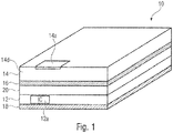
- Fig. 1 1 shows a wafer level package 10 with a chip layer 12, an antenna layer 14 and means for shielding (see reference numeral 16), which are arranged between the chip layer 12 and the antenna layer 14.
- the wafer level package 10 has a contacting layer 18 which is arranged on the underside of the chip layer 12, that is to say on the side of the chip layer 12 opposite the antenna layer 14.
- the antenna layer 14 comprises at least one integrated antenna or an antenna array / group radiator, here the integrated antenna 14a and preferably, but not necessarily, a dielectric region 14d, which is usually arranged between the antenna 14a and the layer 16 with means for screening.
- the means for shielding are formed by a shielding layer 16, that is to say for example by a metallization plane.
- the chip layer 12 includes one or more chips, here the chip 12a (such as an RF chip) embedded in the layer 12.
- the embedding may, for example, by means of a fan-out panel / wafer-level process with the aid of a polymer such.
- B. a molding material.
- the z. B. comprises a redistribution layer and / or insulation layers.
- the chip 12a is connected, for example, via this redistribution layer in the layer and / or via the contacting layer 18.
- the redistribution layer of the layer 20, z. B. via vias be connected to the contacting layer 18.
- a via may also extend from the chip 12a to the integrated antenna 14a to contact it.
- the structure described here offers the advantages with respect to full integration of the antennas 14a, chips 12a, passive components and other system components in the fan-out-panel / wafer level-based system integration platform or module 10.
- the functionality of the platform or of the module 10 completely independent of the circuit board. This is not the case with other state-of-the-art FO-WLP modules such as: Eg eWLB.
- the reflector of the antennas is integrated on the circuit board.
- the functionality of the antennas and also of the platform or of the module depends on the dimensions of the BGA balls, their process fluctuations and also on the printed circuit board.
- these antennas 14 a can be optimized without changing the remaining structure of the platform or of the module 10. This is not the case with other FO-WLP modules, eg. For example, to optimize antennas 14a in eWLB and INFO, the dimensions of the RDL and mold material must be adjusted.
- the fields of the integrated antennas 14a are completely shielded from the chips 12a, passive and other components integrated into the fan-out panel / wafer level based system integration platform or module. This avoids EMC problems. This is not the case in other fan-out modules. Neither in InFo-WLP nor in eWLB are the antennas 14a shielded by the chips 12a.
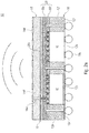
- Fig. 2a shows a wafer level package 10 'with the chip layer 12', the antenna layer 14 ', wherein between the chip layer 12' and antenna layer 14 'on the one hand, the shielding layer 16 and the rewiring plane 20' is provided.
- the contacting plane 18 is also arranged on the underside of the chip layer 12 '.
- the chip layer 12 comprises the two chips 12a and 12b, which is integrated in a so-called fan-out region 12f, comprising other ICs, passive or other system components.
- This fan-out region 12f is typically formed by a polymer or molding material.
- the antenna 14a extends over the entire antenna layer 16 and here in particular over the surface thereof.
- the antenna layer 14 is through, for example Glass substrate, a polymer, a laminate, etc., which forms the respective dielectric 14 'for the antenna 14a'.
- the individual antenna regions or antenna planes are fully embedded in the dielectric 14d '.
- the antenna 14' is connected via a vertical via to the chip 12a ', here an HF chip.
- the Via 16v ' represents the shortest connection. This short signal path with few discontinuities enables signal integrity, even for millimeter waves and terahertz signals.
- the vertical probe 16v ' also an electromagnetic coupling, for. B. be implemented via an apparatus coupling or a near field coupling.
- a transmission line is used.
- the layer 20 ' comprises on the one hand the rewiring plane 20u', z. B. for the signal distribution and the power supply and the insulator 20i ', which is arranged between the chip plane 12' and the rewiring plane 20 '.
- the rewiring plane 20 ' according to further embodiments of one or more metal and dielectric insulating layers.
- passive components such as inductors, resistors, capacitors, filters or other elements may be integrated. Alternatively, an embedding of these passive elements in the mold material of the chip plane 12 ' would be conceivable, in which case these passive elements are contacted via the rewiring plane 12u'.
- the ICs 12a and 12b are connected to the redistribution layer 20u 'via pads 20p'.
- the rewiring plane 20u ' is furthermore contacted with the contacting layer 18 via vias 12v', which project through the molding material 12f or generally through the chip plane 12 '.
- the rewiring layers 20u' including the antenna layer 14a ' can be routed to the package rear side 18 for making contact with the substrate.
- This contacting layer 18 comprises, for example, solderballs or thermal balls, via which the entire package 10 'is contacted.
- solderballs / solder balls 18s or the contacting elements of the contacting layer 18 are likewise provided on the underside of the ICs 12a and 12b, so that the ICs 12a and 12b can be contacted on both sides.
- the antenna substrate 16 + 14' which is made of at least two metal layers 16 and 14a '(shielding means and antenna) and an interposed dielectric layer 14d'.
- the metal layer 16 serves, as already explained above, for shielding the antenna fields from the integrated components.
- the antenna 14a ' can either be constructed from one or more radiating elements (array radiators) and, as already explained, is either galvanically connected by means of a lead or a vias (probe feed) or an electromagnetic coupling (for example aperture-coupled , Proximity Feed).
- the antenna substrate 16 + 14 ' the realization of different antenna configurations, eg.
- the integrated antennas may also be "smart" according to other embodiments, i. H. be configured reconfigurable, controllable, adaptive or smart.
- the electronics eg circuits and / or diodes
- the electronics for reconfigurability which are required for this purpose, can be integrated either in the antenna substrate 16 + 14 ', in the rewiring plane 20', the polymer substrate 12 '(ie together with the ICs 12a and 12b) be.
- the electronics for controlling the antenna eg phase shifter
- the electronics for controlling the antenna are arranged either in the rewiring plane 20 'or in the chip plane 12'.
- the antenna can radiate out of the surface plane, emit to the side (azimuth plane) or in both directions. As illustrated, in the present embodiment, radiation takes place, in particular, out of the main surface of the antenna 14a '.
- the platform or module 10 allows for the radiation of the integrated antennas 16a' into the whole hemisphere (ie, the entire azimuthal and vertical planes) without causing unwanted coupling with other integrated components. This is possible because no other components are integrated at the antenna plane 14 '. That is not the case, eg. With eWLB, since the ICs 12a, 12b and other components are integrated on the same plane as the antennas 14a '. If in the above embodiments 10 and 10 'it was assumed that radiation of the antenna 14a' takes place only from the main surface, as can be seen in FIG Fig. 2d shown, also made a radiation to the side. It should be noted that the wafer level package out Fig. 2d is provided with the reference numeral 10 "and in connection with Fig. 2d will be explained in detail.
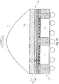
- a modified embodiment of the wafer level package 10 ' namely the wafer level package 10 "is shown, which differs from the wafer level package 10' with respect to the antenna substrate in the antenna layer 14".
- the antenna substrate comprises the elements "antenna 14a""dielectric14d” and means for screening 16.
- the antenna substrate or, in particular, the dielectric 14d may comprise a polymer material, a glass material, an HF laminate or another suitable HF -Material.
- the dielectric layer 14d is provided with periodic holes, ie perforated, whereby the substrate 14 + 16 behaves like a photonic bandgap structure, which leads to the filtering of the surface waves and thus to the improvement of the radiation characteristic
- This increases the edge length of the antenna structure at higher frequencies and reduces the influence of process variations
- the radiation characteristic of the antenna 16a 'can also be achieved by integration of electromagnetic bandgap structures (EBG) either in the antenna substrate 14 "+ 16 or the rewiring plane 20u 'be improved.
- ESG electromagnetic bandgap structures
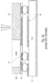
- Fig. 2c 11 shows a further modification starting from the wafer level package 10 ', namely the wafer level package 10'", in which the contacting level 18 (now 18 ') is modified in comparison to the wafer level package 10' in that, in the region of the chip 12a, heat removal means, here a heat sink 18k ', are provided instead of the contacts for underside contacting in order to dissipate the heat from the chip 12a.
- the heat sink 18k' spreads the heat into the surroundings under the chip 12a and the solder balls 18f pass the heat to the next package level, eg the system board.
- a thermally conductive material may be provided between the chip and the heat sink 18k '.
- a heat dissipation via the above-described solder balls 18s would be possible, which is then used as a rule, a thermally conductive material.
- the surface of the chip 12a is exposed.
- the back of the chip can be released directly in the molding process.
- a subsequent regrinding would be possible.
- the typically required for the heat sink 18k 'metallization can either be provided on the chip 12a before packaging or z. B. be applied via a thin film wiring layer or a sputtered layer with galvanic reinforcement.
- the chip substrate 12 ' is provided together with the contacting plane 18 or 18' and the optional redistribution layer 20 '.
- the layer 20 'or after the application of the layer 20', the antenna substrate 14 '+ 16 is then applied.
- This antenna layer 14 '+ 16 may, for. B. over lamination (RF substrate), layer by layer in thin-film technology and a flat bond (glass) are applied.
- the antenna layer 14a ' can already be structured both prior to assembly and can be structured sequentially after assembly.
- the chip substrate 12 ' is connected to the rewiring layer 20' with the antenna substrate 14 '+ 16. This connection thus takes place at wafer level.
- Fig. 2e shows the wafer level package 10 ' Fig. 2a with chip layer 12 ', antenna layer 14', shielding layer 16 and the rewiring plane 20 '.
- the wafer level package 10 ' has an additional lens 21 (means for beam shaping the electromagnetic wave emitted by the antenna) on the top (main surface) adjacent to the antenna 14a'.
- the lens 21 is used for vertical focusing of the antenna beam.
- Fig. 2f again shows the wafer level package 10 ' Fig. 2a in combination with a housing 23 arranged on the upper side (side of the antenna 14 ').
- the housing 23 is preferably made of glass or another non-shielding material.
- the housing 23 may be filled with air or a low-loss dielectric material.
- the housing 23 may also contribute to the beam shaping / focusing of the electromagnetic wave.
- Both housing 23 and lens 21 are applicable together and in combination with all embodiments discussed above / Wafer Level Packages.
- a system in which the wafer level package is connected to (at least) one other (different or the same) wafer level package.
- the connection takes place e.g. over the contacting layer.
- the further wafer level package may e.g. also comprise one or more antennas (array), so that as a result a three-dimensional antenna structure is created.
- the fields of application are manifold.
- the platform 10, 10 ', 10 ", 10'” or the module can be used to develop wireless communication systems that can be used in all frequency ranges of the electromagnetic spectrum, for. B. for WPAN, WLAN, mobile, satellite, etc.
- the platform or module 10-10 '' can be used to develop radar systems that can be used for any applications in all frequency ranges of the electromagnetic spectrum.
- the integrated antenna can be designed as a group radiator or comprise an antenna array, eg with a large number of antennas (> 5 or even> 1000).
- the plurality of antennas are preferably arranged next to one another in such a way that that no or only a minimal overlap with other elements, such as the chips is created.
Landscapes
- Engineering & Computer Science (AREA)
- Microelectronics & Electronic Packaging (AREA)
- Variable-Direction Aerials And Aerial Arrays (AREA)
- Physics & Mathematics (AREA)
- Health & Medical Sciences (AREA)
- Electromagnetism (AREA)
- Toxicology (AREA)
Abstract
Description
- Ausführungsbeispiele der vorliegenden Erfindung beziehen sich auf ein Wafer Level Package mit integrierter Antenne sowie auf ein entsprechendes Herstellungsverfahren. Bevorzugte Ausführungsbeispiele beziehen sich auf eine miniaturisierte Fan-Out-Panel-/Wafer Level-basierte System-Integrationsplattform mit integrierter Antenne.
- Ausführungsbeispiele der vorliegenden Erfindung beziehen sich auf ein Wafer Level Package mit zumindest einem integrierten Antennenelement sowie auf ein entsprechendes Herstellungsverfahren. Bevorzugte Ausführungsbeispiele beziehen sich auf einen Fan-Out-Panel-/Wafer Level-basierte System-Integrationsplattform mit Superstrate integrierten Antennen ohne Umverdrahtungsebene.
- Die Antennen in eWLB und InFO können nicht optimiert werden, ohne die Abmessungen der RDL und des Moldmaterials anzupassen, was die Designfreiheit der Plattform begrenzt.
- Sowohl in eWLB als auch in InFO sind die Felder der integrierten Antennen nicht von den Chips und anderen integrierten Komponenten geschirmt. Die unerwünschte Wechselwirkung kann zu EMV Problemen führen.
- In eWLB kann die Strahlung einer integrierten Antenne nicht die ganze Halbkugel (die gesamte horizontale und vertikale Ebene) abdecken, ohne unerwünschte Kopplung mit anderen integrierten Komponenten zu verursachen. Der Grund dafür ist, dass andere Komponenten auf derselben Ebene wie die Antennen integriert sind. Deshalb besteht der Bedarf nach einem verbesserten Ansatz.
- Aufgabe der vorliegenden Erfindung ist es, ein Konzept zur Integration einer Antenne in einem Wafer Level Package zu schaffen, das einen verbesserten Kompromiss aus Effizienz, Designfreiheit und EMV-Unempfindlichkeit darstellt.
- Die Aufgabe wird durch die unabhängigen Patentansprüche gelöst.
- Ausführungsbeispiele der vorliegenden Erfindung schaffen ein Wafer Level Package mit integrierter Antenne. Das Wafer Level Package hat eine Kontaktierungsschicht, eine Antennenschicht mit integrierter Antenne sowie eine zwischen der Kontaktierungsschicht und der Antennenschicht angeordnete Chipschicht, umfassend zumindest einen Chip. Zwischen der Antennenschicht und der Chipschicht sind Mittel zum Schirmen, wie z. B. eine Schirmebene oder allgemein ein Schirm vorgesehen. Zwischen den Mitteln zum Schirmen und der Chipschicht kann entsprechend Ausführungsbeispielen auch eine Umverdrahtungsschicht ausgebildet sein.
- Ausführungsbeispiele der vorliegenden Erfindung liegt die Erkenntnis zugrunde, dass bei einem schichtweisen Aufbau von Antennenteil und Chipteil es vorteilhaft ist, wenn zwischen diesen zwei Schichten eine Schirmung vorgesehen ist, die sowohl die Chips/ICs der Chipschicht von der Strahlung der Antenne schützt und auch umgekehrt die Antenne vor EMV-Beeinflussungen der Chips bewahrt. Die Anordnung der Umverdrahtungsebene, auf der der Antenne abgewandten Seite des Schirms ist vorteilhaft, da so dieselbe gegenseitige Beeinflussungen durch den Schirm verhindert werden können. Zusätzlich sei erwähnt, dass die Entkopplung von Chiplayer zu Antennenlayer es ermöglicht, beide Ebenen relativ flexibel zu gestalten, da nun kaum oder wenig Wechselwirkungen berücksichtigt werden müssen.
- Entsprechend Ausführungsbeispielen ist die Chipebene durch einen oder mehrere Chips in Kombination mit einem Moldmaterial geformt. Wenn man davon ausgeht, dass die Umverdrahtungsebene auf der der Antenne zugewandten Seite vorliegt, kann entsprechend Ausführungsbeispielen eine Verbindung zwischen der Umverdrahtungsebene und der Kontaktierungsebene beispielsweise durch Vias erfolgen. Alternativ oder additiv hierzu wäre es auch denkbar, dass die Chips beidseitig, das heißt also über die Umverdrahtungsebene und über die Kontaktierungsebene kontaktiert werden. Aufseiten der Kontaktierungsebene können auch statt der Kontaktierung des Chips über diese Ebene auch Mittel zur Temperaturabfuhr für den Chip vorgesehen sein. Insofern ist es nicht nur vorteilhafterweise möglich, sowohl Chipebene als auch Antennenlayer flexibel zu designen, sondern auch wird ein maximaler Freiheitsgrad für die Kontaktierungsebene bzw. das Vorsehen weiterer Elemente wie der Kühlelemente ermöglicht.
- Entsprechend folgenden Ausführungsbeispielen kann zwischen der Antennenschicht und den Mitteln zum Schirmen ein Dielektrikum vorgesehen sein. Dieses Dielektrikum kann entsprechend zusätzlichen Ausführungsbeispielen auch perforiert sein, um so Filterfunktionalität zu ermöglichen. Bei diesem Konzept ist es vorteilhaft, dass sowohl das Material als auch die Dicke des Dielektrizitätslayers variiert werden kann, ohne dass die weiteren Schichten dadurch beeinflusst werden. An dieser Stelle sei auch angemerkt, dass entsprechend Ausführungsbeispielen die Antennenebene auch eine Mehrzahl von Antennenelementen umfassen kann. Analog zu dem Dielektrikum kann auch eine Isolationsschicht zwischen der Chipebene und der oben erläuterten Umverdrahtungsebene vorgesehen sein. Entsprechend wiederum weiteren Ausführungsbeispielen erfolgt die Kontaktierung beispielsweise über ein Via, das durch die Mittel zur Schirmung und eventuell vorhandene weitere Schichten (Dielektrizitätsschicht und Isolationsschicht) durchragt. Dieser Via verbindet also den Chip, wie z. B. den RF-Chip der Chipebene mit ein oder mehreren Antennenelementen. Alternativ kann entsprechend weiteren Ausführungsbeispielen die eine oder mehreren Antennen mittels elektromagnetischer Kopplung kontaktiert werden.
- Weitere Ausführungsbeispiele schaffen ein Verfahren zur Herstellung eines Wafer Level Package mit integrierter Antenne. Bei diesem Verfahren wird zuerst die Kontaktierungsschicht zusammen mit der Chipschicht hergestellt, bevor dann die Antennenschicht auf der Chipschicht mit dazwischen angeordneten Mitteln zum Schirmen angeordnet werden. Hierbei kann das Aufbringen der Antennenschicht beispielsweise mittels Laminieren, flächigem Kleben oder über ein Glassubstrat aufgebracht werden.
- Weiterbildungen sind in den Unteransprüchen definiert. Ausführungsbeispiele der vorliegenden Erfindung werden nachfolgend anhand der Zeichnungen erläutert. Es zeigen:
- Fig. 1
- eine schematische Darstellung eines Wafer Level Package mit integrierter Antenne gemäß einem Basisausführungsbeispiel;
- Fig. 2a-d
- schematische Schnittdarstellungen von Wafer Level Packages mit integrierter Antenne gemäß erweiterten Ausführungsbeispielen;
- Fig. 2e
- eine schematische Schnittdarstellung eines Wafer Level Package mit Linse gemäß einem Ausführungsbeispiel;
- Fig. 2f
- eine schematische Schnittdarstellung eines Wafer Level Package mit Gehäuse gemäß einem Ausführungsbeispiel; und
- Fig. 3a und 3b
- schematische Darstellungen von Wafer Level Packages gemäß Stand-der-Technik-Ansätzen.
- Bevor nachfolgend Ausführungsbeispiele der vorliegende Erfindung anhand der beiliegenden Zeichnungen erläutert werden, sei darauf hingewiesen, dass gleichwirkende Elemente und Strukturen mit gleichen Bezugszeichen versehen sind, so dass die Beschreibung derer aufeinander anwendbar bzw. austauschbar ist.
-
Fig. 1 zeigt ein Wafer Level Package 10 mit einer Chipschicht 12, einer Antennenschicht 14 sowie Mitteln zum Schirmen (vgl. Bezugszeichen 16), die zwischen der Chipschicht 12 und der Antennenschicht 14 angeordnet sind. Zusätzlich weist das Wafer Level Package 10 eine Kontaktierungsschicht 18 auf, die auf der Unterseite der Chipschicht 12, das heißt auf der der Antennenschicht 14 gegenüberliegenden Seite der Chipschicht 12 angeordnet ist. - Die Antennenschicht 14 umfasst zumindest eine integrierte Antenne oder eine Antennenarray/Gruppenstrahler, hier die integrierte Antenne 14a und bevorzugt, aber nicht zwingenderweise ein Dielektrikumbereich 14d, der im Regelfall zwischen der Antenne 14a und der Schicht 16 mit Mitteln zum Schirmen angeordnet ist.
- In diesem Ausführungsbeispiel sind die Mittel zum Schirmen durch eine Schirmschicht 16, das heißt beispielsweise durch eine Metallisierungsebene gebildet.
- Der Chiplayer 12 umfasst eine oder mehrere Chips, hier den Chip 12a (wie z. B. einen RF-Chip), der in die Schicht 12 eingebettet ist. Das Einbetten kann beispielsweise mittels eines Fan-Out-Panel-/Wafer-Level-Prozess unter Zuhilfenahme eines Polymers, wie z. B. eines Moldmaterials erfolgen. Entsprechend Ausführungsbeispielen kann zwischen der Schirmschicht 16 und der Chipschicht 12 auch noch eine weitere Schicht 20 vorgesehen sein, die z. B. eine Umverdrahtungsebene und/oder Isolationslagen umfasst.
- Der Chip 12a wird beispielsweise über diese Umverdrahtungsebene in der Schicht und/oder über die Kontaktierungsschicht 18 verbunden. Entsprechend Ausführungsbeispielen kann die Umverdrahtungsebene der Schicht 20, z. B. über Vias mit der Kontaktierungsschicht 18 verbunden sein. Entsprechend weiteren Ausführungsbeispielen kann auch ein Via sich von dem Chip 12a zu der integrierten Antenne 14a erstrecken, um dieses zu kontaktieren.
- Der hier beschriebene Aufbau bietet den Vorteile bzgl. Vollintegration der Antennen 14a, Chips 12a, passive Komponenten und andere Systemkomponenten in die Fan-Out-Panel-/Wafer Level-basierte System-Integrationsplattform bzw. Modul 10. Dadurch ist die Funktionalität der Plattform bzw. des Moduls 10 komplett unabhängig von der Leiterplatte. Das ist nicht der Fall bei anderen state-of-the-art FO-WLP Modulen wie z. B. eWLB. Hier wird der Reflektor der Antennen auf der Leiterplatte integriert. Dadurch hängt die Funktionalität der Antennen und auch der Plattform bzw. des Moduls von den Abmessungen der BGA Balls, ihren Prozessschwankungen und auch von der Leiterplatte ab.
- Da optional ein separates Substrat 14 für integrierte Antennen 14a benutzt wird, können diese Antennen 14a optimiert werden, ohne den restlichen Aufbau der Plattform bzw. des Moduls 10 zu verändern. Das ist nicht der Fall bei anderen FO-WLP Modulen, z. B. um Antennen 14a in eWLB und InFO zu optimieren, müssen die Abmessungen der RDL und Moldmaterial angepasst werden.
- Die Felder der integrierten Antennen 14a sind komplett geschirmt von den Chips 12a, passiven und anderen Komponenten, die in die Fan-Out-Panel-/Wafer Level-basierte System-Integrationsplattform bzw. Modul integriert sind. Dadurch werden EMV Probleme vermieden. Das ist nicht der Fall in anderen Fan-Out Modulen. Weder in InFo-WLP noch in eWLB sind die Antennen 14a von den Chips 12a geschirmt.
- Bezug nehmend auf
Fig. 2 werden nun erweiterte Ausführungsbeispiele erläutert. -
Fig. 2a zeigt ein Wafer Level Package 10' mit der Chipschicht 12', der Antennenschicht 14', wobei zwischen Chipschicht 12' und Antennenschicht 14' zum einen die Schirmungsschicht 16 sowie die Umverdrahtungsebene 20' vorgesehen ist. Zusätzlich ist auch die Kontaktierungsebene 18 auf der Unterseite der Chipschicht 12' angeordnet. - Die Chipschicht 12' umfasst die zwei Chips 12a und 12b, die in einem sogenannten Fan-out-Bereich 12f, umfassend andere ICs, passive oder andere Systemkomponenten integriert ist. Dieser Fan-out-Bereich 12f ist typischerweise durch ein Polymer bzw. Moldmaterial gebildet.
- Die Antenne 14a' erstreckt sich über die gesamte Antennenschicht 16 und hier insbesondere über die Oberfläche derselben. Die Antennenschicht 14ist beispielsweise durch ein Glassubstrat, ein Polymer, ein Laminat, etc. gebildet, das das jeweilige Dielektrikum 14' für die Antenne 14a' bildet. Wie zu erkennen ist, sind die einzelnen Antennenbereiche bzw. Antennenebenen voll in das Dielektrikum 14d' eingebettet.
- Um die Antenne 14a' zu kontaktieren, ist die Antenne 14' über einen vertikalen Via mit dem Chip 12a', hier einem HF-Chip, verbunden. Wie die Darstellung zu erkennen gibt, stellt der Via 16v' die kürzeste Verbindung dar. Dieser kurze Signalweg mit wenigen Diskontinuitäten ermöglicht die Signalintegrität, auch für Millimeterwellen und Terahertzsignale. Alternativ kann zu der vertikalen Sonde 16v' auch eine elektromagnetische Kopplung, z. B. über eine Apparaturkopplung oder eine Nahfeldkopplung realisiert sein. Weiter wäre es auch denkbar, dass zusätzlich zu der vertikalen Vias 16v' ein planarer Verbinder, wie z. B. eine Transmission-Line eingesetzt wird.
- Die Schicht 20' umfasst zum einen die Umverdrahtungsebene 20u', z. B. für die Signalverteilung und die Stromversorgung sowie den Isolator 20i', der zwischen der Chipebene 12' und der Umverdrahtungsebene 20' angeordnet ist. Die Umverdrahtungsebene 20' besteht entsprechend weiteren Ausführungsbeispielen aus ein oder mehreren Metall- und dielektrischen Isolationsschichten. Zusätzlich können in die Umverdrahtungsebene 20' bzw. insbesondere in die Metallisierungsebene 20u' passive Komponenten, wie z. B. Induktivitäten, Widerstände, Kondensatoren, Filter oder andere Elemente integriert sein. Alternativ wäre eine Einbettung dieser passiven Elemente in das Moldmaterial der Chipebene 12' denkbar, wobei dann diese passiven Elemente über die Umverdrahtungsebene 12u' kontaktiert werden.
- An der Vorderseite sind die ICs 12a und 12b über Pads 20p' mit der Umverdrahtungsebene 20u' verbunden. Die Umverdrahtungsebene 20u' ist des Weiteren über Vias 12v', die durch das Moldmaterial 12f bzw. allgemein durch die Chipebene 12' hindurchragen, mit der Kontaktierungsschicht 18 kontaktiert. Über die elektrisch leitfähige Durchkontaktierung 12v' durch das eingebettete Polymer (Moldcompound) 12f lassen sich die Umverdrahtungslagen 20u' inklusive der Antennenlage 14a' auf die Packagerückseite 18 zur Ankontaktierung zum Substrat routen. Diese Kontaktierungsschicht 18 umfasst beispielsweise Solderballs bzw. Thermalballs, über die das gesamte Package 10' kontaktiert wird. Bei diesem Ausführungsbeispiel ist es auch so, dass auf der Unterseite der ICs 12a und 12b ebenfalls die Solderballs/Lotkugeln 18s bzw. die Kontaktierungselemente der Kontaktierungsschicht 18 vorgesehen sind, so dass die ICs 12a und 12b beidseitig kontaktierbar sind.
- Oberhalb der Umverdrahtungsebene 20u' befindet sich das Antennensubstrat 16+14', das aus mindestens zwei Metalllagen 16 und 14a' (Mittel zum Schirmen und Antenne) sowie eine dazwischen angeordneten Dieleketrikschicht 14d' ausgeführt ist. Die Metalllage 16 dient, wie bereits oben erläutert, zur Schirmung der Antennenfelder von den integrierten Komponenten. Die Antenne 14a' kann entweder aus einem oder aus mehreren strahlenden Elementen (Gruppenstrahler) aufgebaut sein und wird, wie bereits erläutert, entweder galvanisch mit Hilfe einer Leitung oder eines Vias (Probe Feed) oder eines elektromagnetische Kopplung (z. B. Aperture-Coupled, Proximity Feed) angeregt. Je nach gewünschter Abstrahlcharakteristik ermöglicht das Antennensubstrat 16+14' die Realisierung von unterschiedlichen Antennenkonfigurationen, z. B. Patch, Grid-Array, Schlitz, Substratintegrierte Wellenleiter (SIW)-basierte Antennen, Dipol, Monopol, Yagi-Uda, Vivaldi, usw. Die integrierten Antennen können entsprechend weiteren Ausführungsbeispielen auch "intelligent", d. h. rekonfigurierbar, steuerbar, adaptiv bzw. smart ausgeführt sein. Die hierfür regelmäßig erforderliche Elektronik (z. B. Schaltungen und/oder Dioden) für die Rekonfigurierbarkeit kann entweder in dem Antennensubstrat 16+14', in der Umverdrahtungsebene 20', dem Polymersubstrat 12' (also zusammen mit den ICs 12a und 12b) mitintegriert sein. Hierbei wäre es auch entsprechend weiteren Ausführungsbeispielen denkbar, dass die Elektronik für die Steuerung der Antenne (z. B. Phasenschieber) entweder in der Umverdrahtungsebene 20' bzw. in der Chipebene 12' angeordnet ist.
- Ausgehend von der hier vorgestellten Struktur des Wafer Level Package 10' kann in Abhängigkeit von der Antennenkonfiguration die Antenne aus der Oberflächenebene herausstrahlen, zur Seite herausstrahlen (Azimutebene) oder in beide Richtungen. Wie illustriert, erfolgt bei dem hier vorliegenden Ausführungsbeispiel eine Abstrahlung insbesondere aus der Hauptoberfläche der Antenne 14a' heraus.
- Die Plattform bzw. das Modul 10' ermöglicht die Abstrahlung der integrierten Antennen 16a' in die ganze Halbkugel (d. h. in die gesamte azimutale und vertikale Ebene), ohne unerwünschte Kopplung mit anderen integrierten Komponenten zu verursachen. Das ist möglich, weil keine anderen Komponenten auf Antennenebene 14' integriert sind. Das ist nicht der Fall, z. B. mit eWLB, da die ICs 12a, 12b und andere Komponenten auf derselben Ebene wie die Antennen 14a' integriert sind. Wenn bei obigen Ausführungsbeispielen 10 und 10' davon ausgegangen wurde, dass eine Abstrahlung der Antenne 14a' nur aus der Hauptoberfläche heraus erfolgt, kann, wie beispielsweise in
Fig. 2d dargestellt, auch eine Abstrahlung zur Seite erfolgen. Hierbei sei angemerkt, dass das Wafer Level Package ausFig. 2d mit den Bezugszeichen 10" versehen ist und im Zusammenhang mitFig. 2d im Detail erläutert werden wird. - In
Fig. 2b ist ein modifiziertes Ausführungsbeispiel des Wafer Level Packages 10', nämlich das Wafer Level Package 10" dargestellt. Dieses unterscheidet sich von dem Wafer Level Package 10' im Hinblick auf das Antennensubstrat in der Antennenschicht 14". Das Antennensubstrat umfasst die Elemente "Antenne 14a' "Dielektrikum 14d" sowie Mittel zum Schirmen 16. Wie bereits oben erläutert, kann das Antennensubstrat bzw. insbesondere das Dielektrikum 14d" ein Polymermaterial umfassen, ein Glasmaterial, ein HF-Laminat oder ein anderes geeignetes HF-Material. In diesem Ausführungsbeispiel ist die dielektrische Schicht 14d" mit periodischen Löchern versehen, d. h. perforiert. Dadurch verhält sich das Substrat 14+16 wie eine photonische Bandgap-Struktur, die zur Filterung der Oberflächenwellen und damit zur Verbesserung der Abstrahlcharakteristik führt. Weiterhin sinkt der Wert der effektiven Primitivität des Substrats durch die Löcher. Dadurch erhöht sich die Kantenlänge der Antennenstruktur bei höheren Frequenzen und der Einfluss der Prozessschwankungen wird geringer. Die Abstrahlcharakteristik der Antenne 16a' kann auch durch Integration von elektromagnetischen Bandgap-Strukturen (EBG) entweder im Antennensubstrat 14"+16 oder der Umverdrahtungsebene 20u' verbessert werden. -
Fig. 2c zeigt eine weitere Modifikation ausgehend von dem Wafer Level Package 10', nämlich das Wafer Level Package 10'". Bei diesen ist im Vergleich zu dem Wafer Level Package 10' die Kontaktierungsebene 18 (jetzt 18') modifiziert ausgelegt. Die Modifikation ist derart gewählt, dass im Bereich des Chips 12a statt den Kontakten zur Unterseitenkontaktierung Mittel zur Wärmeabfuhr, hier ein Kühlkörper 18k' vorgesehen ist, um die Wärme von dem Chip 12a abzuführen. Der Kühlkörper 18k' spreizt die Wärme in die Umgebung unter dem Chip 12a und die Lotkugeln 18f leiten die Wärme in das nächste Package-Level, z. B. das System-Board weiter. - Entsprechend Ausführungsbeispielen kann zwischen Chip und dem Kühlkörper 18k' ein thermisch leitfähiges Material vorgesehen sein. An dieser Stelle sei angemerkt, dass entsprechend weiteren Ausführungsbeispielen auch eine Wärmeabfuhr über die oben erläuterten Lötkugeln 18s möglich wäre, wobei dann im Regelfall auch ein thermisch leitfähiges Material eingesetzt wird.
- Aus Herstellungssicht gibt es unterschiedliche Möglichkeiten, wie die Oberfläche des Chips 12a freigelegt wird. Entsprechend einer ersten Variante kann die Chiprückseite direkt im Moldprozess freigestellt werden. Alternativ hierzu wäre auch ein nachträgliches Rückschleifen möglich. Die beim Kühlkörper 18k' typischerweise erforderliche Metallisierung kann entweder beim Chip 12a schon vor dem Packaging vorgesehen sein oder z. B. über eine Dünnfilmverdrahtungslage oder eine Sputerlage mit galvanischer Verstärkung aufgebracht werden.
- Auch wenn obige Ausführungsbeispiele insbesondere zusammen mit der Vorrichtung erläutert wurden, schafft ein weiteres Ausführungsbeispiel ein entsprechendes Herstellungsverfahren. Hierbei wird in einem ersten Basisschritt des Chipsubstrat 12' zusammen mit der Kontaktierungsebene 18 bzw. 18' sowie der optionalen Umverdrahtungsebene 20' bereitgestellt. Auch die Schicht 20' bzw. nach dem Aufbringen der Schicht 20' wird dann das Antennensubstrat 14'+16 aufgebracht. Diese Antennenlage 14'+16 kann z. B. über Laminieren (HF-Substrat), schichtweise in Dünnfilmtechnik und über eine flächige Klebung (Glas) aufgebracht werden. Dabei kann die Antennenlage 14a' sowohl vor der Montage bereits strukturiert sein als auch sequentiell nach der Montage strukturiert werden. Das heißt also in anderen Worten ausgedrückt, dass das Chipsubstrat 12' mit der Umverdrahtungslage 20'mit dem Antennensubstrat 14'+16 verbunden wird. Dieses Verbinden erfolgt also auf Waferlevel.
-
Fig. 2e zeigt das Wafer Level Package 10' ausFig. 2a mit Chipschicht 12', Antennenschicht 14', Schirmungsschicht 16 sowie die Umverdrahtungsebene 20'. In diesem Ausführungsbeispiel weist das Wafer Level Package 10' eine zusätzliche Linse 21 (Mittel zur Strahlformung der elektromagnetischen Welle ausgesendet durch die Antenne) auf der Oberseite (Hauptoberfläche), benachbart zur Antenne 14a'. Die Linse 21 dient zur vertikale Fokussierung des Antennenstrahls. -
Fig. 2f zeigt wiederum das Wafer Level Package 10' ausFig. 2a in Kombination mit einem auf der Oberseite (Seite der Antenne 14') angeordneten Gehäuse 23. Das Gehäuse 23 ist bevorzugt aus Glas oder einem anderen nicht schirmenden Material. Das Gehäuse 23 kann z.B. mit Luft oder einem dielektrischen Material mit geringen Verlusten gefüllt sein. Ferner kann das Gehäuse 23 auch zur Strahlformung / Fokussierung der elektromagnetischen Welle beitragen. - Sowohl Gehäuse 23 als auch Linse 21 sind zusammen und in Kombination mit allen oben erläuterten Ausführungsbeispielen / Wafer Level Packages anwendbar.
- Gemäß einem weiteren Ausführungsbeispiel wird ein System geschaffen, bei dem das Wafer Level Package mit (zumindest) einem weiteren (andersartigem oder gleichem) Wafer Level Package verbunden ist. Die Vebindung erfolgt z.B. über die Kontaktierungsschicht. Das weitere Wafer Level Package kann z.B. ebenfalls ein oder mehrerer Antennen (Array) umfassen, sodass im Ergebnis eine dreidimensionale Antennenstruktur geschaffen wird.
- Alle oben genannten Ausführungsbeispiele, insbesondere die Ausführungsbeispiele aus den
Fig. 2a-d haben gemein, dass eine kurze Verbindungsstrecke 16v' ohne viele geometrische Diskontinuitäten von dem Front-End-IC 12a zu der Antenne 14a' ermöglicht werden, was zu einer guten Signalintegrität, z. B. im Millimeter-Wellenbereich oder Terahertz-Bereich führt. Die Plattform bzw. das Modul 10', 10" und 10'" ermöglicht die Integration von Antennenkonfigurationen mit beliebigen Anbringungsmöglichkeiten. Das ist insbesondere mit anderen FOWLP-Konfigurationen nicht der Fall. Des Weiteren ermöglichen, hier insbesondere im Zusammenhang mitFig. 2c und2d dargestellt, die oben erläuterten Strukturen eine integrierte Lösung für das thermische Management. - Die Anwendungsgebiete sind mannigfaltig. Die Plattform 10, 10', 10", 10'" bzw. das Modul kann eingesetzt werden, um drahtlose Kommunikationssysteme, die in allen Frequenzbereichen des elektromagnetischen Spektrums eingesetzt werden können, zu entwickeln, z. B. für WPAN, WLAN, Mobilfunk, Satelliten, usw.
- Das kann auch eingesetzt werden, um drahtlose Sensorsysteme, die für beliebige Anwendungen in allen Frequenzbereichen des elektromagnetischen Spektrums eingesetzt werden können, zu entwickeln.
- Weiterhin kann die Plattform bzw. das Modul 10-10'" eingesetzt werden, um Radarsysteme, die für beliebige Anwendungen in allen Frequenzbereichen des elektromagnetischen Spektrums eingesetzt werden können, zu entwickeln.
- Wie oben bereits erwähnt, kann die integrierten Antenne als Gruppenstrahler ausgeführt sein oder ein Antennenarray, z.B. mit einer Vielzahl von Antennen (>5 oder sogar >1000,) umfassen, Hier sind die mehreren Antennen bevorzugt nebeneinander so angeordnet, dass kein oder nur ein minimaler Überlapp mit weiteren Elementen, wie den Chips entsteht.
- An dieser Stelle sei angemerkt, dass obige Ausführungsbeispiele nur illustrativ sind, während der Schutzbereich durch die nachfolgenden Patentansprüche festgelegt wird.
-
- [1] T. Meyer, G. Ofner, S. Bradl, M. Brunnbauer, R. Hagen; Embedded Wafer Level Ball Grid Array (eWLB); Proceedings of EPTC 2008, Singapore.
- [2] B. Keser, C. Amrine, T. Duong, O. Fay, S. Hayes, G. Leal, W. Lytle, D. Mitchell, R. Wenzel; The Redistributed Chip Package: A Breakthrough for Advanced Packaging, Proceedings of ECTC 2007, Reno/Nevada, USA.
- [3] Chung-Hao Tsai et Al., Array Antenna Integrated Fan-out Wafer Level Packaging (InFO-WLP) for Millimeter Wave System Applications", 2013 IEEE International Electronic Devices Meeting (IEDM), 9-11 Dec. 2013, pp. 25.1.1 - 25.1.4.
- [4] Christopher Beck, et al., Industrial mmWave Radar Sensor in Embedded Wafer Level BGA Packaging Technology", IEEE SENSORS JOURNAL, VOL. 16, NO. 17, SEPTEMBER 1, 2016
Claims (20)
- Wafer Level Package (10, 10', 10", 10'") mit integrierter Antenne, mit folgenden Merkmalen:einer Kontaktierungsschicht (18, 18');einer Antennenschicht (14, 14') mit der integrierten Antenne; undeiner zwischen der Kontaktierungsschicht (18, 18') und der Antennenschicht (14, 14') angeordneten Chipschicht (12'), umfassend zumindest einen Chip,wobei zwischen der Antennenschicht (14, 14') und der Chipschicht (12') Mittel zum Schirmen (16) ausgebildet sind.
- Wafer Level Package (10, 10', 10", 10'") gemäß Anspruch 1, wobei die Mittel zum Schirmen (16) ein Schild umfassen.
- Wafer Level Package (10, 10', 10", 10'") gemäß Anspruch 1 oder 2, wobei zwischen den Mittel zum Schirmen (16) und der Chipschicht (12') eine Umverdrahtungsschicht (20u') ausgebildet ist.
- Wafer Level Package (10, 10', 10", 10'") gemäß Anspruch 3, wobei eine Isolationsschicht (20i') zwischen der Umverdrahtungsschicht (20u') und der Chipschicht (12') ausgebildet ist.
- Wafer Level Package (10, 10', 10", 10'") gemäß einem der vorherigen Ansprüche,
wobei die integrierte Antenne als Gruppenstrahler ausgeführt ist oder ein Antennenarray umfasst. - Wafer Level Package (10, 10', 10", 10'") gemäß einem der vorherigen Ansprüche,
wobei die Chipschicht (12') ein Moldmaterial umfasst, das neben dem zumindest einen Chip (12) angeordnet ist. - Wafer Level Package (10, 10', 10", 10'") gemäß einem der vorherigen Ansprüche,
wobei der Chip (12) beidseitig kontaktiert ist. - Wafer Level Package (10, 10', 10", 10'") gemäß einem der vorherigen Ansprüche,
wobei die integrierte Antenne (14a, 14a') mittels eines Vias (16u') mit dem Chip (12) verbunden ist, das durch weitere Schichten hindurchragt,
oder wobei die integrierte Antenne (14a, 14a') mittels elektromagnetischer Kopplung mit dem Chip (12) verbunden ist. - Wafer Level Package (10, 10', 10", 10'") gemäß einem der Ansprüche 1 bis 6,
wobei der Chip (12) aufseiten der Antennenschicht (14, 14') kontaktiert wird und/oder wobei der Chip (12) auf einer der Antennenschicht (14, 14') gegenüberliegenden Seite Mittel zur Temperaturabfuhr aufweist. - Wafer Level Package (10, 10', 10", 10'") gemäß einem der vorherigen Ansprüche,
wobei die Antenneneben ein Dielektrikum (14d, 14d', 14d") umfasst, das zwischen der integrierten Antenne und dem den Mitteln zum Schirmen angeordnet ist. - Wafer Level Package (10, 10', 10", 10'") gemäß Anspruch 10, wobei das Dielektrikum (14d, 14d', 14d") perforiert ist.
- Wafer Level Package (10, 10', 10", 10'") gemäß einem der vorherigen Ansprüche,
wobei die integrierte Antenne (14a, 14a') zumindest zwei Antennenelemente umfasst. - Wafer Level Package (10, 10', 10", 10'") gemäß einem der vorherigen Ansprüche,
wobei die Chipschicht (12') eine Mehrzahl von Chips (12) umfasst. - Wafer Level Package (10, 10', 10", 10'") gemäß einem der vorherigen Ansprüche,
wobei das Wafer Level Package (10, 10', 10", 10'") eine Linse (19) umfasst, die ausgebildet ist, mit der integrierten Antenne zusammenzuwirken. - Wafer Level Package (10, 10', 10", 10'") gemäß einem der vorherigen Ansprüche,
wobei die Mittel zum Schirmen durch eine Schirmschicht geformt sind;
wobei zwischen den Mittel zum Schirmen (16) und der Chipschicht (12') eine Umverdrahtungsschicht (20u') ausgebildet ist, wobei eine Isolationsschicht (20i') zwischen der Umverdrahtungsschicht (20u') und der Chipschicht (12') ausgebildet ist. - Wafer Level Package (10, 10', 10", 10'") gemäß Anspruch 15, wobei in der Kontaktierungsebene (18) im Bereich des Chips (12a) Mittel zur Wärmeabfuhr (18k') vorgesehen sind.
- System umfassend das Wafer Level Package (10, 10', 10", 10'") gemäß einem der Ansprüche 1 bis 16, wobei ein weiteres Wafer Level Package über die Kontaktierungsschicht (18, 18') mit dem Wafer Level Package (10, 10', 10") verbunden ist.
- Verfahren zur Herstellung eines Wafer Level Package (10, 10', 10", 10'") mit integrierter Antenne, mit folgenden Schritten:Anordnen einer Kontaktierungsschicht (18, 18');Anordnen einer Chipschicht (12') umfassend zumindest einen Chip (12) auf der Kontaktierungsschicht (18, 18');Anordnen von Mittel zum Schirmen (16) auf der Chipschicht (12'); undAnordnen einer Antennenschicht (14, 14') auf den Mittel zum Schirmen (16); .
- Verfahren gemäß Anspruch 18, wobei die Antennenschicht (14, 14') mittels Laminieren und/oder über eine flächige Klebung und/oder über ein Glas aufgebracht wird.
- Verfahren gemäß Anspruch 18 oder 19, wobei die Mittel zum Schirmen durch eine Schirmschicht geformt sind;
wobei zwischen den Mittel zum Schirmen (16) und der Chipschicht (12') eine Umverdrahtungsschicht (20u') ausgebildet ist.
Applications Claiming Priority (1)
| Application Number | Priority Date | Filing Date | Title |
|---|---|---|---|
| DE102017200122.4A DE102017200122B4 (de) | 2017-01-05 | 2017-01-05 | Wafer Level Package mit integrierten Antennen und Mittel zum Schirmen, System dieses umfassend und Verfahren zu dessen Herstellung |
Publications (2)
| Publication Number | Publication Date |
|---|---|
| EP3346493A1 true EP3346493A1 (de) | 2018-07-11 |
| EP3346493B1 EP3346493B1 (de) | 2021-08-18 |
Family
ID=60954861
Family Applications (1)
| Application Number | Title | Priority Date | Filing Date |
|---|---|---|---|
| EP18150174.3A Active EP3346493B1 (de) | 2017-01-05 | 2018-01-03 | Wafer level package mit integrierten antennen und mittel zum schirmen |
Country Status (3)
| Country | Link |
|---|---|
| US (1) | US10978778B2 (de) |
| EP (1) | EP3346493B1 (de) |
| DE (1) | DE102017200122B4 (de) |
Families Citing this family (18)
| Publication number | Priority date | Publication date | Assignee | Title |
|---|---|---|---|---|
| US20180294569A1 (en) * | 2017-04-07 | 2018-10-11 | Skyworks Solutions, Inc. | Radio-frequency module with integrated shield layer antenna and integrated cavity-based antenna |
| US11069978B2 (en) | 2017-04-07 | 2021-07-20 | Skyworks Solutions, Inc. | Method of manufacturing a radio-frequency module with a conformal shield antenna |
| US10593635B2 (en) * | 2018-03-27 | 2020-03-17 | Nxp B.V. | Multi-die and antenna array device |
| DE102018205670A1 (de) * | 2018-04-13 | 2019-10-17 | Fraunhofer-Gesellschaft zur Förderung der angewandten Forschung e.V. | Hermetisch abgedichtete Moduleinheit mit integrierten Antennen |
| US11201119B2 (en) | 2018-06-06 | 2021-12-14 | At&S Austria Technologie & Systemtechnik Aktiengesellschaft | RF functionality and electromagnetic radiation shielding in a component carrier |
| KR102145219B1 (ko) * | 2018-07-27 | 2020-08-18 | 삼성전자주식회사 | 반도체 패키지 및 이를 포함하는 안테나 모듈 |
| US11605877B2 (en) | 2018-09-07 | 2023-03-14 | Advanced Semiconductor Engineering, Inc. | Semiconductor device package and method of manufacturing the same |
| WO2020066085A1 (ja) * | 2018-09-25 | 2020-04-02 | 株式会社村田製作所 | 平面型ワイヤレス受電回路モジュール |
| DE102018220712B4 (de) | 2018-11-30 | 2024-06-13 | Fraunhofer-Gesellschaft zur Förderung der angewandten Forschung e.V. | Wafer-level packaging-basiertes modul sowie verfahren zur herstellung desselben |
| CN109473404A (zh) * | 2018-12-06 | 2019-03-15 | 麦堆微电子技术(上海)有限公司 | 一种微波芯片封装结构 |
| DE102019124237A1 (de) * | 2018-12-28 | 2020-07-02 | Taiwan Semiconductor Manufacturing Co., Ltd. | Heterogene antenne im fan-out-package |
| US20200212536A1 (en) * | 2018-12-31 | 2020-07-02 | Texas Instruments Incorporated | Wireless communication device with antenna on package |
| US10903561B2 (en) | 2019-04-18 | 2021-01-26 | Advanced Semiconductor Engineering, Inc. | Semiconductor device package and method of manufacturing the same |
| US11784416B2 (en) | 2020-01-06 | 2023-10-10 | Raytheon Company | Tunable radio frequency (RF) absorber and thermal heat spreader |
| US12400978B2 (en) * | 2021-05-18 | 2025-08-26 | Samsung Electronics Co., Ltd. | Semiconductor package |
| US11924963B2 (en) | 2022-02-03 | 2024-03-05 | Raytheon Company | Printed-circuit isolation barrier for co-site interference mitigation |
| US12418103B2 (en) * | 2022-06-14 | 2025-09-16 | Tron Future Tech Inc. | Antenna package structure |
| US12451589B2 (en) | 2023-02-21 | 2025-10-21 | Tron Future Tech Inc. | Antenna package and method for manufacturing an antenna package |
Citations (4)
| Publication number | Priority date | Publication date | Assignee | Title |
|---|---|---|---|---|
| US20080186247A1 (en) * | 2006-08-03 | 2008-08-07 | International Business Machines Corporation | VERSATILE Si-BASED PACKAGING WITH INTEGRATED PASSIVE COMPONENTS FOR mmWAVE APPLICATIONS |
| US20130292808A1 (en) * | 2012-05-04 | 2013-11-07 | Advanced Semiconductor Engineering, Inc. | Semiconductor package integrated with conformal shield and antenna |
| DE102013108075A1 (de) * | 2012-08-02 | 2014-02-06 | Infineon Technologies Ag | Chip-Gehäuse und Verfahren zur Herstellung eines Chip-Gehäuses |
| US20150380386A1 (en) * | 2014-06-26 | 2015-12-31 | Michael B. Vincent | Microelectronic packages having embedded sidewall substrates and methods for the producing thereof |
Family Cites Families (29)
| Publication number | Priority date | Publication date | Assignee | Title |
|---|---|---|---|---|
| GB2216320B (en) | 1988-02-29 | 1992-08-19 | Int Standard Electric Corp | Apparatus and methods for the selective addition of noise to templates employed in automatic speech recognition systems |
| US6770955B1 (en) | 2001-12-15 | 2004-08-03 | Skyworks Solutions, Inc. | Shielded antenna in a semiconductor package |
| US6933450B2 (en) | 2002-06-27 | 2005-08-23 | Kyocera Corporation | High-frequency signal transmitting device |
| JP4109039B2 (ja) | 2002-08-28 | 2008-06-25 | 株式会社ルネサステクノロジ | 電子タグ用インレットおよびその製造方法 |
| US7126541B2 (en) | 2002-11-19 | 2006-10-24 | Farrokh Mohamadi | Beam forming phased array system in a transparent substrate |
| US7634034B2 (en) | 2004-07-01 | 2009-12-15 | Staccato Communications, Inc. | Payload boundary detection during multiband receiver synchronization |
| DE102006023123B4 (de) | 2005-06-01 | 2011-01-13 | Infineon Technologies Ag | Abstandserfassungsradar für Fahrzeuge mit einem Halbleitermodul mit Komponenten für Höchstfrequenztechnik in Kunststoffgehäuse und Verfahren zur Herstellung eines Halbleitermoduls mit Komponenten für ein Abstandserfassungsradar für Fahrzeuge in einem Kunststoffgehäuse |
| DE102006007381A1 (de) | 2006-02-15 | 2007-08-23 | Infineon Technologies Ag | Halbleiterbauelement für einen Ultraweitband-Standard in der Ultrahochfrequenz-Kommunikation und Verfahren zur Herstellung desselben |
| JP4316607B2 (ja) | 2006-12-27 | 2009-08-19 | 株式会社東芝 | アンテナ装置及び無線通信装置 |
| US8331892B2 (en) | 2008-03-29 | 2012-12-11 | Qualcomm Incorporated | Method and system for DC compensation and AGC |
| US8115682B2 (en) | 2008-12-29 | 2012-02-14 | Auden Techno Corp. | Multi-band HAC compatible antenna module |
| US8278749B2 (en) | 2009-01-30 | 2012-10-02 | Infineon Technologies Ag | Integrated antennas in wafer level package |
| US7848108B1 (en) | 2009-08-06 | 2010-12-07 | International Business Machines Corporation | Heatsink with periodically patterned baseplate structure |
| US8558637B2 (en) | 2010-05-12 | 2013-10-15 | Mediatek Inc. | Circuit device with signal line transition element |
| US9007273B2 (en) * | 2010-09-09 | 2015-04-14 | Advances Semiconductor Engineering, Inc. | Semiconductor package integrated with conformal shield and antenna |
| US8451618B2 (en) | 2010-10-28 | 2013-05-28 | Infineon Technologies Ag | Integrated antennas in wafer level package |
| US8890304B2 (en) | 2011-06-08 | 2014-11-18 | Tessera, Inc. | Fan-out microelectronic unit WLP having interconnects comprising a matrix of a high melting point, a low melting point and a polymer material |
| US8754514B2 (en) | 2011-08-10 | 2014-06-17 | Taiwan Semiconductor Manufacturing Company, Ltd. | Multi-chip wafer level package |
| US20150207236A1 (en) | 2012-07-25 | 2015-07-23 | The University Of Melbourne | Antenna unit |
| US9431369B2 (en) | 2012-12-13 | 2016-08-30 | Taiwan Semiconductor Manufacturing Company, Ltd. | Antenna apparatus and method |
| US9461355B2 (en) | 2013-03-29 | 2016-10-04 | Intel Corporation | Method apparatus and material for radio frequency passives and antennas |
| EP3080841A4 (de) | 2013-12-09 | 2017-08-23 | Intel Corporation | Antenne auf keramik für einen kompakten chip |
| US9362234B2 (en) | 2014-01-07 | 2016-06-07 | Freescale Semiconductor, Inc. | Shielded device packages having antennas and related fabrication methods |
| EP3032580B1 (de) | 2014-03-14 | 2018-06-20 | Fuji Electric Co., Ltd. | Kühlvorrichtung und halbleiterbauelement mit besagter kühlvorrichtung |
| FR3032556B1 (fr) | 2015-02-11 | 2017-03-17 | Commissariat Energie Atomique | Dispositif de transmission rf a reflecteur d'ondes electromagnetiques integre |
| JP6429680B2 (ja) | 2015-03-03 | 2018-11-28 | パナソニック株式会社 | アンテナ一体型モジュール及びレーダ装置 |
| US20160329299A1 (en) | 2015-05-05 | 2016-11-10 | Mediatek Inc. | Fan-out package structure including antenna |
| US11195787B2 (en) | 2016-02-17 | 2021-12-07 | Infineon Technologies Ag | Semiconductor device including an antenna |
| US10032722B2 (en) | 2016-05-31 | 2018-07-24 | Taiwan Semiconductor Manufacturing Co., Ltd. | Semiconductor package structure having am antenna pattern and manufacturing method thereof |
-
2017
- 2017-01-05 DE DE102017200122.4A patent/DE102017200122B4/de not_active Expired - Fee Related
-
2018
- 2018-01-03 US US15/860,926 patent/US10978778B2/en active Active
- 2018-01-03 EP EP18150174.3A patent/EP3346493B1/de active Active
Patent Citations (4)
| Publication number | Priority date | Publication date | Assignee | Title |
|---|---|---|---|---|
| US20080186247A1 (en) * | 2006-08-03 | 2008-08-07 | International Business Machines Corporation | VERSATILE Si-BASED PACKAGING WITH INTEGRATED PASSIVE COMPONENTS FOR mmWAVE APPLICATIONS |
| US20130292808A1 (en) * | 2012-05-04 | 2013-11-07 | Advanced Semiconductor Engineering, Inc. | Semiconductor package integrated with conformal shield and antenna |
| DE102013108075A1 (de) * | 2012-08-02 | 2014-02-06 | Infineon Technologies Ag | Chip-Gehäuse und Verfahren zur Herstellung eines Chip-Gehäuses |
| US20150380386A1 (en) * | 2014-06-26 | 2015-12-31 | Michael B. Vincent | Microelectronic packages having embedded sidewall substrates and methods for the producing thereof |
Also Published As
| Publication number | Publication date |
|---|---|
| US10978778B2 (en) | 2021-04-13 |
| DE102017200122B4 (de) | 2020-07-23 |
| US20180191052A1 (en) | 2018-07-05 |
| EP3346493B1 (de) | 2021-08-18 |
| DE102017200122A1 (de) | 2018-07-05 |
Similar Documents
| Publication | Publication Date | Title |
|---|---|---|
| EP3346493B1 (de) | Wafer level package mit integrierten antennen und mittel zum schirmen | |
| EP3346544B1 (de) | Waver level package mit integrierter oder eingebetteter antenne | |
| DE102017223561B4 (de) | Hochfrequenzbauelement-Packages und Verfahren zum Bilden derselben | |
| EP3346548B1 (de) | Modulanordnung mit eingebetteten komponenten und einer integrierten antenne, vorrichtung mit modulanordnungen und verfahren zur herstellung | |
| DE102014118563B4 (de) | Halbleitergehäuse mit integrierter Mikrowellenkomponente und Verfahren zu deren Herstellung | |
| EP3346494B1 (de) | Wafer level package mit zumindest einem integrierten antennenelement | |
| DE102011085348B4 (de) | Integrierte Antennen in einem Waferebenengehäuse und Herstellungsverfahren dafür | |
| DE102015108267B4 (de) | Gehäuse für ein robust ausgeführtes Automobilradar-Teilsystem | |
| DE102017202578B4 (de) | Halbleitervorrichtung, die eine Antenne enthält, und Verfahren zur Herstellung einer Halbleitervorrichtung | |
| DE102016110862B4 (de) | Modul und Verfahren zur Herstellung einer Vielzahl von Modulen | |
| DE112016006695B4 (de) | Gehäuse auf Antennengehäuse und Verfahren zu dessen Herstellung | |
| DE102006023123B4 (de) | Abstandserfassungsradar für Fahrzeuge mit einem Halbleitermodul mit Komponenten für Höchstfrequenztechnik in Kunststoffgehäuse und Verfahren zur Herstellung eines Halbleitermoduls mit Komponenten für ein Abstandserfassungsradar für Fahrzeuge in einem Kunststoffgehäuse | |
| DE112017001710T5 (de) | Mikrowellenantenneneinrichtung, Verpackungs- und Herstellungsverfahren | |
| DE112019001942T5 (de) | Packungsstrukturen und -verfahren für integrierte antennen-arrays | |
| DE102013111581A1 (de) | Halbleiterpackages mit integrierter Antenne und Verfahren zu deren Herstellung | |
| WO2016135099A1 (de) | Reflektor mit einer elektronischen schaltung und antennenvorrichtung mit einem reflektor | |
| DE112017007887T5 (de) | Antennenpackage mit kugel-anbringungs-array zum verbinden von antennen- und basissubstraten | |
| DE102010036978A1 (de) | Bauelement mit einer ringförmigen Metallstruktur und Verfahren | |
| DE102018220712A1 (de) | Wafer-level packaging-basiertes modul sowie verfahren zur herstellung desselben | |
| DE102013111569B4 (de) | Halbleiterpackages mit integrierter Antenne und Verfahren zu deren Herstellung | |
| EP3346549B1 (de) | Elektronisches modul mit integrierter antenne und verfahren zur herstellung | |
| DE102023126148A1 (de) | Package mit Selbstabschirmung | |
| EP3346547B1 (de) | Modulanordnung mit integrierter antenne und eingebetteten komponenten sowie verfahren zur herstellung einer modulanordnung | |
| DE102019128779A1 (de) | Hochfrequenz-Vorrichtung mit Hochfrequenz-Signalführungselement und zugehöriges Herstellungsverfahren | |
| DE102012221940B4 (de) | Modul zur drahtlosen Kommunikation und Verfahren zum Herstellen eines Moduls zur drahtlosen Kommunikation |
Legal Events
| Date | Code | Title | Description |
|---|---|---|---|
| PUAI | Public reference made under article 153(3) epc to a published international application that has entered the european phase |
Free format text: ORIGINAL CODE: 0009012 |
|
| STAA | Information on the status of an ep patent application or granted ep patent |
Free format text: STATUS: THE APPLICATION HAS BEEN PUBLISHED |
|
| AK | Designated contracting states |
Kind code of ref document: A1 Designated state(s): AL AT BE BG CH CY CZ DE DK EE ES FI FR GB GR HR HU IE IS IT LI LT LU LV MC MK MT NL NO PL PT RO RS SE SI SK SM TR |
|
| AX | Request for extension of the european patent |
Extension state: BA ME |
|
| STAA | Information on the status of an ep patent application or granted ep patent |
Free format text: STATUS: REQUEST FOR EXAMINATION WAS MADE |
|
| 17P | Request for examination filed |
Effective date: 20190111 |
|
| RBV | Designated contracting states (corrected) |
Designated state(s): AL AT BE BG CH CY CZ DE DK EE ES FI FR GB GR HR HU IE IS IT LI LT LU LV MC MK MT NL NO PL PT RO RS SE SI SK SM TR |
|
| STAA | Information on the status of an ep patent application or granted ep patent |
Free format text: STATUS: EXAMINATION IS IN PROGRESS |
|
| 17Q | First examination report despatched |
Effective date: 20200903 |
|
| GRAP | Despatch of communication of intention to grant a patent |
Free format text: ORIGINAL CODE: EPIDOSNIGR1 |
|
| STAA | Information on the status of an ep patent application or granted ep patent |
Free format text: STATUS: GRANT OF PATENT IS INTENDED |
|
| RIC1 | Information provided on ipc code assigned before grant |
Ipc: H01L 21/60 20060101ALI20210122BHEP Ipc: H01L 23/538 20060101ALI20210122BHEP Ipc: H01L 23/552 20060101AFI20210122BHEP Ipc: H01L 23/66 20060101ALI20210122BHEP Ipc: H01L 23/485 20060101ALI20210122BHEP |
|
| INTG | Intention to grant announced |
Effective date: 20210226 |
|
| GRAS | Grant fee paid |
Free format text: ORIGINAL CODE: EPIDOSNIGR3 |
|
| GRAA | (expected) grant |
Free format text: ORIGINAL CODE: 0009210 |
|
| STAA | Information on the status of an ep patent application or granted ep patent |
Free format text: STATUS: THE PATENT HAS BEEN GRANTED |
|
| AK | Designated contracting states |
Kind code of ref document: B1 Designated state(s): AL AT BE BG CH CY CZ DE DK EE ES FI FR GB GR HR HU IE IS IT LI LT LU LV MC MK MT NL NO PL PT RO RS SE SI SK SM TR |
|
| REG | Reference to a national code |
Ref country code: GB Ref legal event code: FG4D Free format text: NOT ENGLISH |
|
| REG | Reference to a national code |
Ref country code: CH Ref legal event code: EP |
|
| REG | Reference to a national code |
Ref country code: DE Ref legal event code: R096 Ref document number: 502018006594 Country of ref document: DE |
|
| REG | Reference to a national code |
Ref country code: IE Ref legal event code: FG4D Free format text: LANGUAGE OF EP DOCUMENT: GERMAN Ref country code: AT Ref legal event code: REF Ref document number: 1422401 Country of ref document: AT Kind code of ref document: T Effective date: 20210915 |
|
| REG | Reference to a national code |
Ref country code: LT Ref legal event code: MG9D |
|
| REG | Reference to a national code |
Ref country code: NL Ref legal event code: MP Effective date: 20210818 |
|
| PG25 | Lapsed in a contracting state [announced via postgrant information from national office to epo] |
Ref country code: SE Free format text: LAPSE BECAUSE OF FAILURE TO SUBMIT A TRANSLATION OF THE DESCRIPTION OR TO PAY THE FEE WITHIN THE PRESCRIBED TIME-LIMIT Effective date: 20210818 Ref country code: RS Free format text: LAPSE BECAUSE OF FAILURE TO SUBMIT A TRANSLATION OF THE DESCRIPTION OR TO PAY THE FEE WITHIN THE PRESCRIBED TIME-LIMIT Effective date: 20210818 Ref country code: HR Free format text: LAPSE BECAUSE OF FAILURE TO SUBMIT A TRANSLATION OF THE DESCRIPTION OR TO PAY THE FEE WITHIN THE PRESCRIBED TIME-LIMIT Effective date: 20210818 Ref country code: ES Free format text: LAPSE BECAUSE OF FAILURE TO SUBMIT A TRANSLATION OF THE DESCRIPTION OR TO PAY THE FEE WITHIN THE PRESCRIBED TIME-LIMIT Effective date: 20210818 Ref country code: FI Free format text: LAPSE BECAUSE OF FAILURE TO SUBMIT A TRANSLATION OF THE DESCRIPTION OR TO PAY THE FEE WITHIN THE PRESCRIBED TIME-LIMIT Effective date: 20210818 Ref country code: NO Free format text: LAPSE BECAUSE OF FAILURE TO SUBMIT A TRANSLATION OF THE DESCRIPTION OR TO PAY THE FEE WITHIN THE PRESCRIBED TIME-LIMIT Effective date: 20211118 Ref country code: PT Free format text: LAPSE BECAUSE OF FAILURE TO SUBMIT A TRANSLATION OF THE DESCRIPTION OR TO PAY THE FEE WITHIN THE PRESCRIBED TIME-LIMIT Effective date: 20211220 Ref country code: BG Free format text: LAPSE BECAUSE OF FAILURE TO SUBMIT A TRANSLATION OF THE DESCRIPTION OR TO PAY THE FEE WITHIN THE PRESCRIBED TIME-LIMIT Effective date: 20211118 Ref country code: LT Free format text: LAPSE BECAUSE OF FAILURE TO SUBMIT A TRANSLATION OF THE DESCRIPTION OR TO PAY THE FEE WITHIN THE PRESCRIBED TIME-LIMIT Effective date: 20210818 |
|
| PG25 | Lapsed in a contracting state [announced via postgrant information from national office to epo] |
Ref country code: PL Free format text: LAPSE BECAUSE OF FAILURE TO SUBMIT A TRANSLATION OF THE DESCRIPTION OR TO PAY THE FEE WITHIN THE PRESCRIBED TIME-LIMIT Effective date: 20210818 Ref country code: LV Free format text: LAPSE BECAUSE OF FAILURE TO SUBMIT A TRANSLATION OF THE DESCRIPTION OR TO PAY THE FEE WITHIN THE PRESCRIBED TIME-LIMIT Effective date: 20210818 Ref country code: GR Free format text: LAPSE BECAUSE OF FAILURE TO SUBMIT A TRANSLATION OF THE DESCRIPTION OR TO PAY THE FEE WITHIN THE PRESCRIBED TIME-LIMIT Effective date: 20211119 |
|
| PG25 | Lapsed in a contracting state [announced via postgrant information from national office to epo] |
Ref country code: NL Free format text: LAPSE BECAUSE OF FAILURE TO SUBMIT A TRANSLATION OF THE DESCRIPTION OR TO PAY THE FEE WITHIN THE PRESCRIBED TIME-LIMIT Effective date: 20210818 |
|
| RAP4 | Party data changed (patent owner data changed or rights of a patent transferred) |
Owner name: FRAUNHOFER-GESELLSCHAFT ZUR FOERDERUNG DER ANGEWANDTEN FORSCHUNG E.V. |
|
| PG25 | Lapsed in a contracting state [announced via postgrant information from national office to epo] |
Ref country code: DK Free format text: LAPSE BECAUSE OF FAILURE TO SUBMIT A TRANSLATION OF THE DESCRIPTION OR TO PAY THE FEE WITHIN THE PRESCRIBED TIME-LIMIT Effective date: 20210818 |
|
| REG | Reference to a national code |
Ref country code: DE Ref legal event code: R097 Ref document number: 502018006594 Country of ref document: DE |
|
| PG25 | Lapsed in a contracting state [announced via postgrant information from national office to epo] |
Ref country code: SM Free format text: LAPSE BECAUSE OF FAILURE TO SUBMIT A TRANSLATION OF THE DESCRIPTION OR TO PAY THE FEE WITHIN THE PRESCRIBED TIME-LIMIT Effective date: 20210818 Ref country code: SK Free format text: LAPSE BECAUSE OF FAILURE TO SUBMIT A TRANSLATION OF THE DESCRIPTION OR TO PAY THE FEE WITHIN THE PRESCRIBED TIME-LIMIT Effective date: 20210818 Ref country code: RO Free format text: LAPSE BECAUSE OF FAILURE TO SUBMIT A TRANSLATION OF THE DESCRIPTION OR TO PAY THE FEE WITHIN THE PRESCRIBED TIME-LIMIT Effective date: 20210818 Ref country code: EE Free format text: LAPSE BECAUSE OF FAILURE TO SUBMIT A TRANSLATION OF THE DESCRIPTION OR TO PAY THE FEE WITHIN THE PRESCRIBED TIME-LIMIT Effective date: 20210818 Ref country code: CZ Free format text: LAPSE BECAUSE OF FAILURE TO SUBMIT A TRANSLATION OF THE DESCRIPTION OR TO PAY THE FEE WITHIN THE PRESCRIBED TIME-LIMIT Effective date: 20210818 Ref country code: AL Free format text: LAPSE BECAUSE OF FAILURE TO SUBMIT A TRANSLATION OF THE DESCRIPTION OR TO PAY THE FEE WITHIN THE PRESCRIBED TIME-LIMIT Effective date: 20210818 |
|
| PLBE | No opposition filed within time limit |
Free format text: ORIGINAL CODE: 0009261 |
|
| STAA | Information on the status of an ep patent application or granted ep patent |
Free format text: STATUS: NO OPPOSITION FILED WITHIN TIME LIMIT |
|
| 26N | No opposition filed |
Effective date: 20220519 |
|
| PG25 | Lapsed in a contracting state [announced via postgrant information from national office to epo] |
Ref country code: IT Free format text: LAPSE BECAUSE OF FAILURE TO SUBMIT A TRANSLATION OF THE DESCRIPTION OR TO PAY THE FEE WITHIN THE PRESCRIBED TIME-LIMIT Effective date: 20210818 |
|
| PG25 | Lapsed in a contracting state [announced via postgrant information from national office to epo] |
Ref country code: SI Free format text: LAPSE BECAUSE OF FAILURE TO SUBMIT A TRANSLATION OF THE DESCRIPTION OR TO PAY THE FEE WITHIN THE PRESCRIBED TIME-LIMIT Effective date: 20210818 Ref country code: MC Free format text: LAPSE BECAUSE OF FAILURE TO SUBMIT A TRANSLATION OF THE DESCRIPTION OR TO PAY THE FEE WITHIN THE PRESCRIBED TIME-LIMIT Effective date: 20210818 |
|
| REG | Reference to a national code |
Ref country code: CH Ref legal event code: PL |
|
| REG | Reference to a national code |
Ref country code: BE Ref legal event code: MM Effective date: 20220131 |
|
| PG25 | Lapsed in a contracting state [announced via postgrant information from national office to epo] |
Ref country code: LU Free format text: LAPSE BECAUSE OF NON-PAYMENT OF DUE FEES Effective date: 20220103 |
|
| PG25 | Lapsed in a contracting state [announced via postgrant information from national office to epo] |
Ref country code: BE Free format text: LAPSE BECAUSE OF NON-PAYMENT OF DUE FEES Effective date: 20220131 |
|
| PG25 | Lapsed in a contracting state [announced via postgrant information from national office to epo] |
Ref country code: LI Free format text: LAPSE BECAUSE OF NON-PAYMENT OF DUE FEES Effective date: 20220131 Ref country code: CH Free format text: LAPSE BECAUSE OF NON-PAYMENT OF DUE FEES Effective date: 20220131 |
|
| PG25 | Lapsed in a contracting state [announced via postgrant information from national office to epo] |
Ref country code: IE Free format text: LAPSE BECAUSE OF NON-PAYMENT OF DUE FEES Effective date: 20220103 |
|
| P01 | Opt-out of the competence of the unified patent court (upc) registered |
Effective date: 20230524 |
|
| REG | Reference to a national code |
Ref country code: AT Ref legal event code: MM01 Ref document number: 1422401 Country of ref document: AT Kind code of ref document: T Effective date: 20230103 |
|
| PG25 | Lapsed in a contracting state [announced via postgrant information from national office to epo] |
Ref country code: HU Free format text: LAPSE BECAUSE OF FAILURE TO SUBMIT A TRANSLATION OF THE DESCRIPTION OR TO PAY THE FEE WITHIN THE PRESCRIBED TIME-LIMIT; INVALID AB INITIO Effective date: 20180103 |
|
| PG25 | Lapsed in a contracting state [announced via postgrant information from national office to epo] |
Ref country code: AT Free format text: LAPSE BECAUSE OF NON-PAYMENT OF DUE FEES Effective date: 20230103 |
|
| PG25 | Lapsed in a contracting state [announced via postgrant information from national office to epo] |
Ref country code: MK Free format text: LAPSE BECAUSE OF FAILURE TO SUBMIT A TRANSLATION OF THE DESCRIPTION OR TO PAY THE FEE WITHIN THE PRESCRIBED TIME-LIMIT Effective date: 20210818 Ref country code: CY Free format text: LAPSE BECAUSE OF FAILURE TO SUBMIT A TRANSLATION OF THE DESCRIPTION OR TO PAY THE FEE WITHIN THE PRESCRIBED TIME-LIMIT Effective date: 20210818 Ref country code: AT Free format text: LAPSE BECAUSE OF NON-PAYMENT OF DUE FEES Effective date: 20230103 |
|
| PG25 | Lapsed in a contracting state [announced via postgrant information from national office to epo] |
Ref country code: MT Free format text: LAPSE BECAUSE OF FAILURE TO SUBMIT A TRANSLATION OF THE DESCRIPTION OR TO PAY THE FEE WITHIN THE PRESCRIBED TIME-LIMIT Effective date: 20210818 |
|
| REG | Reference to a national code |
Ref country code: DE Ref legal event code: R079 Ref document number: 502018006594 Country of ref document: DE Free format text: PREVIOUS MAIN CLASS: H01L0023552000 Ipc: H10W0042200000 |
|
| PG25 | Lapsed in a contracting state [announced via postgrant information from national office to epo] |
Ref country code: TR Free format text: LAPSE BECAUSE OF FAILURE TO SUBMIT A TRANSLATION OF THE DESCRIPTION OR TO PAY THE FEE WITHIN THE PRESCRIBED TIME-LIMIT Effective date: 20210818 |
|
| PGFP | Annual fee paid to national office [announced via postgrant information from national office to epo] |
Ref country code: GB Payment date: 20260122 Year of fee payment: 9 |
|
| PGFP | Annual fee paid to national office [announced via postgrant information from national office to epo] |
Ref country code: DE Payment date: 20260120 Year of fee payment: 9 |
|
| PGFP | Annual fee paid to national office [announced via postgrant information from national office to epo] |
Ref country code: AT Payment date: 20260410 Year of fee payment: 5 |
|
| PGFP | Annual fee paid to national office [announced via postgrant information from national office to epo] |
Ref country code: FR Payment date: 20260127 Year of fee payment: 9 |