EP3345070B1 - Systems and methods for dynamically adjusting memory state transition timers - Google Patents
Systems and methods for dynamically adjusting memory state transition timers Download PDFInfo
- Publication number
- EP3345070B1 EP3345070B1 EP16751453.8A EP16751453A EP3345070B1 EP 3345070 B1 EP3345070 B1 EP 3345070B1 EP 16751453 A EP16751453 A EP 16751453A EP 3345070 B1 EP3345070 B1 EP 3345070B1
- Authority
- EP
- European Patent Office
- Prior art keywords
- memory
- state transition
- power state
- optimal value
- parameters
- Prior art date
- Legal status (The legal status is an assumption and is not a legal conclusion. Google has not performed a legal analysis and makes no representation as to the accuracy of the status listed.)
- Active
Links
- 230000007704 transition Effects 0.000 title claims description 50
- 238000000034 method Methods 0.000 title claims description 28
- 238000004590 computer program Methods 0.000 claims description 4
- 230000003116 impacting effect Effects 0.000 claims description 3
- 238000012544 monitoring process Methods 0.000 claims 2
- 238000005457 optimization Methods 0.000 description 14
- 238000010586 diagram Methods 0.000 description 9
- 238000012545 processing Methods 0.000 description 6
- 238000004891 communication Methods 0.000 description 5
- 230000003068 static effect Effects 0.000 description 5
- 230000001413 cellular effect Effects 0.000 description 3
- 230000006870 function Effects 0.000 description 3
- 101100498818 Arabidopsis thaliana DDR4 gene Proteins 0.000 description 2
- 102100036725 Epithelial discoidin domain-containing receptor 1 Human genes 0.000 description 2
- 101710131668 Epithelial discoidin domain-containing receptor 1 Proteins 0.000 description 2
- 238000005516 engineering process Methods 0.000 description 2
- 230000003287 optical effect Effects 0.000 description 2
- 238000013515 script Methods 0.000 description 2
- 238000010845 search algorithm Methods 0.000 description 2
- 230000004075 alteration Effects 0.000 description 1
- 230000000295 complement effect Effects 0.000 description 1
- 239000013078 crystal Substances 0.000 description 1
- 230000007774 longterm Effects 0.000 description 1
- 230000007334 memory performance Effects 0.000 description 1
- 229910044991 metal oxide Inorganic materials 0.000 description 1
- 150000004706 metal oxides Chemical class 0.000 description 1
- 238000010295 mobile communication Methods 0.000 description 1
- 239000004065 semiconductor Substances 0.000 description 1
- 238000004088 simulation Methods 0.000 description 1
- 238000006467 substitution reaction Methods 0.000 description 1
- 239000000758 substrate Substances 0.000 description 1
- 238000012360 testing method Methods 0.000 description 1
- 238000012546 transfer Methods 0.000 description 1
Images


Classifications
-
- G—PHYSICS
- G06—COMPUTING; CALCULATING OR COUNTING
- G06F—ELECTRIC DIGITAL DATA PROCESSING
- G06F1/00—Details not covered by groups G06F3/00 - G06F13/00 and G06F21/00
- G06F1/26—Power supply means, e.g. regulation thereof
- G06F1/32—Means for saving power
- G06F1/3203—Power management, i.e. event-based initiation of a power-saving mode
- G06F1/3234—Power saving characterised by the action undertaken
- G06F1/3296—Power saving characterised by the action undertaken by lowering the supply or operating voltage
-
- G—PHYSICS
- G06—COMPUTING; CALCULATING OR COUNTING
- G06F—ELECTRIC DIGITAL DATA PROCESSING
- G06F1/00—Details not covered by groups G06F3/00 - G06F13/00 and G06F21/00
- G06F1/26—Power supply means, e.g. regulation thereof
- G06F1/32—Means for saving power
- G06F1/3203—Power management, i.e. event-based initiation of a power-saving mode
- G06F1/3206—Monitoring of events, devices or parameters that trigger a change in power modality
- G06F1/3228—Monitoring task completion, e.g. by use of idle timers, stop commands or wait commands
-
- G—PHYSICS
- G06—COMPUTING; CALCULATING OR COUNTING
- G06F—ELECTRIC DIGITAL DATA PROCESSING
- G06F1/00—Details not covered by groups G06F3/00 - G06F13/00 and G06F21/00
- G06F1/26—Power supply means, e.g. regulation thereof
- G06F1/32—Means for saving power
- G06F1/3203—Power management, i.e. event-based initiation of a power-saving mode
- G06F1/3234—Power saving characterised by the action undertaken
- G06F1/325—Power saving in peripheral device
- G06F1/3275—Power saving in memory, e.g. RAM, cache
-
- Y—GENERAL TAGGING OF NEW TECHNOLOGICAL DEVELOPMENTS; GENERAL TAGGING OF CROSS-SECTIONAL TECHNOLOGIES SPANNING OVER SEVERAL SECTIONS OF THE IPC; TECHNICAL SUBJECTS COVERED BY FORMER USPC CROSS-REFERENCE ART COLLECTIONS [XRACs] AND DIGESTS
- Y02—TECHNOLOGIES OR APPLICATIONS FOR MITIGATION OR ADAPTATION AGAINST CLIMATE CHANGE
- Y02D—CLIMATE CHANGE MITIGATION TECHNOLOGIES IN INFORMATION AND COMMUNICATION TECHNOLOGIES [ICT], I.E. INFORMATION AND COMMUNICATION TECHNOLOGIES AIMING AT THE REDUCTION OF THEIR OWN ENERGY USE
- Y02D10/00—Energy efficient computing, e.g. low power processors, power management or thermal management
Definitions
- Portable computing devices e.g., cellular telephones, smart phones, tablet computers, portable digital assistants (PDAs), portable game consoles, wearable devices, and other battery-powered devices
- PDAs portable digital assistants
- portable game consoles wearable devices
- other battery-powered devices as are for example described in US 2014/157026 A1 , WO 2013/062701 A1 , and US 6 820 209 B1
- To keep pace with these service enhancements such devices have become more powerful and more complex.
- Portable computing devices now commonly include a system on chip (SoC) comprising one or more chip components embedded on a single substrate (e.g., one or more central processing units (CPUs), a graphics processing unit (GPU), digital signal processors, etc.).
- SoC system on chip
- the SoC may be coupled to one or more volatile memory modules or devices, such as, dynamic random access memory (DRAM) via double data rate (DDR) high-performance data and control interface(s).
- DRAM dynamic random access memory
- DDR double data rate
- DDR memory e.g., DDR1, DDR2, DDR3, DDR4, etc.
- DDR memory devices have clock timer settings (e.g., a power down timer, a page close timer, a self-refresh timer), which may impact the idle time duration required to enter the lower power mode.
- clock timer settings e.g., a power down timer, a page close timer, a self-refresh timer
- SoC and system manufacturers may program static values for the idle timers based on lab simulation and test results.
- the static idle timer values may be determined to provide power and performance for overall key use cases. In operation, the predetermined static idle timer values are used regardless of the various use case changes, DDR types and models, changes in power versus performance priority, etc.
- the use of predetermined static settings for the idle timers may yield less than an optimal power and/or performance due to dynamically changing factors.
- the optimal idle timer values may vary depending on DDR types, models, and generations, as well as changing operational factors, such as, memory traffic patterns, memory operating frequencies, memory traffic amounts, and power versus performance priorities.
- One embodiment of a method comprises receiving parameters corresponding to usage or performance of a memory device coupled to a processor in a computing device, wherein the parameters comprise memory utilization percentage and memory operating frequency.
- An optimal value is determined for one or more memory power state transition timer settings for the memory device, wherein the determining comprises accessing a look-up table to determine the optimal value based on the parameters.
- a current value is updated for the memory power state transition timer settings with the optimal value.
- the computer system comprises means for receiving parameters corresponding to usage or performance of a memory device coupled to a processor in a computing device, wherein the parameters comprise memory utilization percentage and memory operating frequency. Also, the system comprises means for determining an optimal value for one or more memory power state transition timer settings for the memory device, wherein the determining comprises accessing a look-up table to determine the optimal value based on the parameters. Further, the system comprises means for updating a current value for the memory power state transition timer settings with the optimal value.
- an “application” may also include files having executable content, such as: object code, scripts, byte code, markup language files, and patches.
- an “application” referred to herein may also include files that are not executable in nature, such as documents that may need to be opened or other data files that need to be accessed.
- content may also include files having executable content, such as: object code, scripts, byte code, markup language files, and patches.
- content referred to herein, may also include files that are not executable in nature, such as documents that may need to be opened or other data files that need to be accessed.
- a component may be, but is not limited to being, a process running on a processor, a processor, an object, an executable, a thread of execution, a program, and/or a computer.
- an application running on a computing device and the computing device may be a component.
- One or more components may reside within a process and/or thread of execution, and a component may be localized on one computer and/or distributed between two or more computers.
- these components may execute from various computer readable media having various data structures stored thereon.
- the components may communicate by way of local and/or remote processes such as in accordance with a signal having one or more data packets (e.g., data from one component interacting with another component in a local system, distributed system, and/or across a network such as the Internet with other systems by way of the signal).
- a portable computing device may include a cellular telephone, a pager, a PDA, a smartphone, a navigation device, or a hand-held computer with a wireless connection or link.
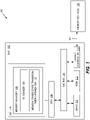
- FIG. 1 illustrates a system 100 comprising a system on chip (SoC) 102 electrically coupled to one or more memory devices 104.
- SoC system on chip
- the SoC 102 comprises various on-chip components interconnected via a SoC bus 114.
- the SoC 102 comprises one or more memory clients that request memory resources from the memory device(s) 104.
- the memory clients may comprise one or more processing units (e.g., central processing unit (CPU) 106, a graphics processing unit (GPU), a digital signal processor (DSP), etc.), a video encoder, or other clients requesting read/write access to the memory device(s) 104.
- the SoC 102 may further comprise on-chip memory, such as, static random access memory (SRAM) 110 and read only memory (ROM) 112.
- SRAM static random access memory
- ROM read only memory
- system 100 may be implemented in any computing device, including a personal computer, a workstation, a server, a portable computing device (PCD), such as a cellular telephone, a smartphone, a portable digital assistant (PDA), a portable game console, a navigation device, a tablet computer, a wearable device, such as a sports watch, a fitness tracking device, etc., or other battery-powered, web-enabled devices.
- PCD portable computing device
- PDA portable digital assistant
- navigation device such as a sports watch, a fitness tracking device, etc.
- wearable device such as a sports watch, a fitness tracking device, etc., or other battery-powered, web-enabled devices.
- Memory controller 108 on SoC 102 is electrically coupled to the memory device(s) 104 via a bus 124.
- Memory controller 108 manages the flow of data going to and from the memory device(s) 104.
- Memory controller 108 generally comprises the logic for reading and writing to the memory device(s) 104.
- the memory device(s) 104 comprise dynamic random access memory (DRAM) device(s) and the bus 124 comprises a high-performance random access memory (RAM) bus.
- DRAM dynamic random access memory
- RAM high-performance random access memory
- the memory controller 108 and the DRAM devices may support any existing or future generations of double data rate (DRR) interfaces (e . g ., DDR1, DDR2, DDR3, DDR4, etc.).
- DDR double data rate
- the memory device(s) 104 and the memory controller 108 may be configured to support two or more memory power states or modes. Each memory power state or mode may be selectively controlled by the memory controller 108 to provide different combinations of memory power consumption and/or memory performance. At least one of the memory power states comprises a relatively lower power memory state for conserving memory power consumption.
- an operating system (O/S 116) executed by the CPU 106 may comprise a memory manager 118.
- the memory manager 118 generally comprises the logic for allocating memory in the memory device(s) 104 to memory clients.
- the memory manager 118 may comprise a scheduler component 120 for scheduling memory read/write operations to the memory device(s) 104.
- the memory manager 118 may further comprise a memory power state transition timer optimization component 122, which generally comprises the logic for dynamically adjusting one or more timer settings used by the memory device(s) 104 to transition from one memory power state to another power state.
- the memory power state transition timer optimization component 122 is configured to determine optimal power-saving values for the one or more timer settings used to enter a lower power memory state.
- the memory power state transition timer optimization component 122 may be implemented in the O/S/ 116, as illustrated in FIG. 1 , or in hardware or firmware.
- FIG. 2 illustrates an embodiment of a method 200 implemented in the system 100 for dynamically adjusting memory power state transition timers to yield a power savings in a low power memory state.
- the memory power state transition timer optimization component 122 receives one or more parameters impacting the usage or performance of the memory device 104. It should be appreciated that the received parameters may be monitored via the operating system 116, the memory manager 118, and/or the scheduler 120. Furthermore, the received parameters may vary depending on, for example, the type of memory device or other components in the system 100. In an embodiment, the received parameters comprise memory operating frequencies and memory utilization percentage. The received parameters may also identify a type, model, and or vendor for the memory device(s) 104.
- the memory power state transition timer optimization component 122 determines, based on the one or more received parameters, whether current values for one or more memory power state transition timer settings are to be updated by determining an optimal value for the one or more memory power state transition timer settings.
- the memory power state transition timer optimization component 122 may monitor and detect dynamic changes in the received parameters to determine whether current values for the memory power state transition timers are less than optimal for power conservation in the low power memory state.
- the memory power state transition timers may vary depending on the type, generation, model, etc. of the memory device(s) 104.
- the timers may comprise DDR idle timers such as, for example, a power down timer, a page close timer, or a self-refresh timer.
- the memory power state transition timer optimization component 122 updates the values for the memory power state transition timers with an optimal value based on or more of the received parameters.
- the optimal value may be provided to and stored in the memory controller 108 for use when entering the low power memory state (block 208).
- FIG. 3 is a block diagram illustrating exemplary data inputs and outputs for an embodiment of the memory power state transition timer optimization component 122.
- the memory power state transition timer optimization component 122 is configured to determine optimal values for DDR idle timer settings 312 used by DRAM devices to enter a low power memory state.
- a DRAM controller 304 may store current values for the DDR idle timer settings 312 in one or more registers 310.
- the memory power state transition timer optimization component 122 may monitor and/or receive various data inputs 302, as illustrated at arrow 306.
- the data inputs 302 may comprise various information related to memory usage such as, for example, memory traffic patterns, memory operating frequencies, memory traffic amounts or utilization percentage, and the memory device type, vendor, or model.
- the data inputs 302 may also comprise information related to memory power and/or performance priorities or modes, application(s) being executed, battery life remaining, or any other conditions or parameters that may impact the optimal values for the DDR idle timer settings.
- FIG. 4 is a timing diagram 400 illustrating the operation of various exemplary DDR idle timers that may be dynamically adjusted by the memory power state transition timer optimization component 122.
- Timing diagram 400 shows operation of a power down idle timer 402, a page close idle timer 404, and a self-refresh idle timer 406.
- the duration of idle timers 402, 404, and 406 may be controlled by corresponding idle timer settings 312 stored in the register(s) 310.
- the power down idle timer 402 has a current value of 64 DDR clock cycles.
- the page close idle timer 404 has a current value of 128 DDR clock cycles.
- the self-refresh idle timer 404 has a current value of 50 cycles of a crystal oscillator.
- the memory power state transition timer optimization component 122 may determine optimal values for timers 402, 404, and 406 based on the data inputs 302.
- the memory power state transition timer optimization component 122 accesses a look-up table to determine the idle timer settings (i.e., data output(s)) that correspond to one or more of the data inputs 302.
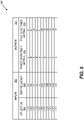
- FIG. 5 illustrates a look-up table 500 for determining optimal power down timer and page down timer settings based on a memory utilization percentage and a memory operating frequency.
- Column 502 illustrates values for combinations of a memory utilization percentage 506 and a DDR frequency 508. For each combination of input values in column 502, the table 500 lists the corresponding output values in column 504.
- the corresponding output value for the power down timer is identified in column 510, and the corresponding output value for the page close timer is identified in column 512.
- the look-up table 500 determines that the values for the power down timer and the page close timer should be updated to 4 and 64 DDR cycles, respectively. It should be appreciated that the inputs 502 and outputs 504 may be based on simulated data and programmed into the registers 310 as default values.
- FIG. 7 illustrates another example of a look-up table 700 for determining the optimal power down timer and page close timer settings based on use case types, which represents an alternative to the claimed look-up table and only facilitates the understanding of the claimed invention.
- the use case types listed in column 706 define the table inputs.
- the table 700 lists the corresponding output values in column 704.
- the corresponding output value for the power down timer is identified in column 708, and the corresponding output value for the page close timer is identified in column 710.
- FIG. 7 illustrates another example of a look-up table 700 for determining the optimal power down timer and page close timer settings based on use case types, which represents an alternative to the claimed look-up table and only facilitates the understanding of the claimed invention.
- the use case types listed in column 706 define the table inputs.
- the table 700 lists the corresponding output values in column 704.
- the corresponding output value for the power down timer is identified in column 708, and the corresponding output value for the page close timer is identified
- the use case types may comprise one or more of the following: a voice call using wideband code division multiple access (WCDMA) or Global System for Mobile Communication (GSM); a voice call over Long-Term Evolution (LTE); LTE data downloading; graphics benchmark application; DDR benchmark application; or any other use cases.
- WCDMA wideband code division multiple access
- GSM Global System for Mobile Communication
- LTE Long-Term Evolution
- LTE data downloading graphics benchmark application
- DDR benchmark application DDR benchmark application
- the inputs 702 and outputs 704 may also be based on simulated data and programmed into the registers 310 as default values.
- the memory power state transition timer optimization component 122 may be configured to calculate the optimal values for the DDR idle timer settings based on an average idle timer duration.
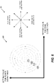
- FIG. 6 is a graph 600 illustrating an example for determining the optimal idle timer settings using an iterative search method, which represents an alternative to the claimed look-up table determination and only facilitates the understanding of the claimed invention.
- the x-axis represents values for the page close timer, and the y-axis represents values for the power down timer.
- a search algorithm may iteratively search for optimal x and y values that yield a lower average memory power.
- the search method may start with an initial value combination at X0.
- the search algorithm may estimate power and/or performance for adjacent value combinations. As illustrated in FIG.
- adjacent values with larger and smaller values for both the power down timer and the page close timer may be searched to determine whether an adjacent value yields better power and/or performance.
- the search method may be configured to iteratively identify subsequent value combinations X1, X2, X3, etc. until an optimal value combination is determined that yields the lowest possible average memory power.
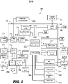
- FIG. 8 illustrates the system 100 incorporated in an exemplary portable computing device (PCD) 800.
- PCD portable computing device
- the SoC 322 may include a multicore CPU 802.
- the multicore CPU 802 may include a zeroth core 810, a first core 812, and an Nth core 814.
- One of the cores may comprise, for example, a graphics processing unit (GPU) with one or more of the others comprising the CPU.
- GPU graphics processing unit
- a display controller 328 and a touch screen controller 330 may be coupled to the CPU 802.
- the touch screen display 806 external to the on-chip system 322 may be coupled to the display controller 328 and the touch screen controller 330.
- FIG. 8 further shows that a video encoder 334, e.g., a phase alternating line (PAL) encoder, a sequential color a memoire (SECAM) encoder, or a national television system(s) committee (NTSC) encoder, is coupled to the multicore CPU 802. Further, a video amplifier 336 is coupled to the video encoder 334 and the touch screen display 806. Also, a video port 338 is coupled to the video amplifier 336. As shown in FIG. 8 , a universal serial bus (USB) controller 340 is coupled to the multicore CPU 802. Also, a USB port 342 is coupled to the USB controller 340. Memory 104 may be coupled to the SoC 322 (as illustrated in FIG. 1 ).
- PAL phase alternating line
- SECAM sequential color a memoire
- NTSC national television system(s) committee
- a digital camera 348 may be coupled to the multicore CPU 802.
- the digital camera 348 is a charge-coupled device (CCD) camera or a complementary metal-oxide semiconductor (CMOS) camera.
- CCD charge-coupled device
- CMOS complementary metal-oxide semiconductor
- a stereo audio coder-decoder (CODEC) 350 may be coupled to the multicore CPU 802.
- an audio amplifier 352 may coupled to the stereo audio CODEC 350.
- a first stereo speaker 354 and a second stereo speaker 356 are coupled to the audio amplifier 352.
- FIG. 8 shows that a microphone amplifier 358 may be also coupled to the stereo audio CODEC 350.
- a microphone 360 may be coupled to the microphone amplifier 358.
- a frequency modulation (FM) radio tuner 362 may be coupled to the stereo audio CODEC 350.
- an FM antenna 364 is coupled to the FM radio tuner 362.
- stereo headphones 366 may be coupled to the stereo audio CODEC 350.
- FM frequency modulation
- FIG. 8 further illustrates that a radio frequency (RF) transceiver 368 may be coupled to the multicore CPU 802.
- An RF switch 370 may be coupled to the RF transceiver 368 and an RF antenna 372.
- a keypad 204 may be coupled to the multicore CPU 802.
- a mono headset with a microphone 376 may be coupled to the multicore CPU 802.
- a vibrator device 378 may be coupled to the multicore CPU 802.
- FIG. 8 also shows that a power supply 380 may be coupled to the on-chip system 322.
- the power supply 380 is a direct current (DC) power supply that provides power to the various components of the PCD 800 that require power.
- the power supply is a rechargeable DC battery or a DC power supply that is derived from an alternating current (AC) to DC transformer that is connected to an AC power source.
- AC alternating current
- FIG. 8 further indicates that the PCD 800 may also include a network card 388 that may be used to access a data network, e.g., a local area network, a personal area network, or any other network.
- the network card 388 may be a Bluetooth network card, a WiFi network card, a personal area network (PAN) card, a personal area network ultra-low-power technology (PeANUT) network card, a television/cable/satellite tuner, or any other network card well known in the art.
- the network card 388 may be incorporated into a chip, i.e., the network card 388 may be a full solution in a chip, and may not be a separate network card 388.
- the touch screen display 806, the video port 338, the USB port 342, the camera 348, the first stereo speaker 354, the second stereo speaker 356, the microphone 360, the FM antenna 364, the stereo headphones 366, the RF switch 370, the RF antenna 372, the keypad 374, the mono headset 376, the vibrator 378, and the power supply 380 may be external to the on-chip system 322.
- one or more of the method steps described herein may be stored in the memory as computer program instructions, such as the modules described above. These instructions may be executed by any suitable processor in combination or in concert with the corresponding module to perform the methods described herein.
- the functions described may be implemented in hardware, software, firmware, or any combination thereof. If implemented in software, the functions may be stored on or transmitted as one or more instructions or code on a computer-readable medium.
- Computer-readable media include both computer storage media and communication media including any medium that facilitates transfer of a computer program from one place to another.
- a storage media may be any available media that may be accessed by a computer.
- such computer-readable media may comprise RAM, ROM, EEPROM, NAND flash, NOR flash, M-RAM, P-RAM, R-RAM, CD-ROM or other optical disk storage, magnetic disk storage or other magnetic storage devices, or any other medium that may be used to carry or store desired program code in the form of instructions or data structures and that may be accessed by a computer.
- Disk and disc includes compact disc (“CD”), laser disc, optical disc, digital versatile disc (“DVD”), floppy disk and blu-ray disc where disks usually reproduce data magnetically, while discs reproduce data optically with lasers. Combinations of the above should also be included within the scope of computer-readable media.
Landscapes
- Engineering & Computer Science (AREA)
- Theoretical Computer Science (AREA)
- Physics & Mathematics (AREA)
- General Engineering & Computer Science (AREA)
- General Physics & Mathematics (AREA)
- Power Sources (AREA)
- Memory System (AREA)
Applications Claiming Priority (2)
| Application Number | Priority Date | Filing Date | Title |
|---|---|---|---|
| US14/846,306 US9690364B2 (en) | 2015-09-04 | 2015-09-04 | Systems and methods for dynamically adjusting memory state transition timers |
| PCT/US2016/045673 WO2017039950A1 (en) | 2015-09-04 | 2016-08-05 | Systems and methods for dynamically adjusting memory state transition timers |
Publications (2)
| Publication Number | Publication Date |
|---|---|
| EP3345070A1 EP3345070A1 (en) | 2018-07-11 |
| EP3345070B1 true EP3345070B1 (en) | 2022-04-13 |
Family
ID=56684785
Family Applications (1)
| Application Number | Title | Priority Date | Filing Date |
|---|---|---|---|
| EP16751453.8A Active EP3345070B1 (en) | 2015-09-04 | 2016-08-05 | Systems and methods for dynamically adjusting memory state transition timers |
Country Status (8)
| Country | Link |
|---|---|
| US (1) | US9690364B2 (zh) |
| EP (1) | EP3345070B1 (zh) |
| JP (1) | JP2018527676A (zh) |
| KR (1) | KR20180048993A (zh) |
| CN (1) | CN107924225B (zh) |
| BR (1) | BR112018004376B1 (zh) |
| TW (1) | TWI630610B (zh) |
| WO (1) | WO2017039950A1 (zh) |
Families Citing this family (10)
| Publication number | Priority date | Publication date | Assignee | Title |
|---|---|---|---|---|
| US20180335828A1 (en) * | 2017-05-19 | 2018-11-22 | Qualcomm Incorporated | Systems and methods for reducing memory power consumption via device-specific customization of ddr interface parameters |
| US10642337B2 (en) * | 2017-08-03 | 2020-05-05 | Qualcomm Incorporated | Active power management in a computing device subsystem based on micro-idle duration |
| KR102480017B1 (ko) * | 2017-08-11 | 2022-12-21 | 삼성전자 주식회사 | 입출력 장치의 성능 및 전력소모를 조절하는 메모리 컨트롤러, 어플리케이션 프로세서 및 메모리 컨트롤러의 동작방법 |
| US11176986B2 (en) | 2019-12-30 | 2021-11-16 | Advanced Micro Devices, Inc. | Memory context restore, reduction of boot time of a system on a chip by reducing double data rate memory training |
| CN114020140B (zh) * | 2020-02-12 | 2023-11-28 | 地平线(上海)人工智能技术有限公司 | 控制硬件模块的方法及装置、电子设备和存储介质 |
| US20200310517A1 (en) * | 2020-05-28 | 2020-10-01 | Intel Corporation | Adaptive lower power state entry and exit |
| US11640251B2 (en) | 2021-01-20 | 2023-05-02 | Western Digital Technologies, Inc. | Early transition to low power mode for data storage devices |
| US11934252B2 (en) * | 2021-03-17 | 2024-03-19 | Micron Technology, Inc. | Shallow hibernate power state |
| US20230065593A1 (en) * | 2021-08-31 | 2023-03-02 | Micron Technology, Inc. | Memory traffic monitoring |
| US11886220B2 (en) | 2022-05-05 | 2024-01-30 | Qualcomm Incorporated | Dynamic power-down management in a computing device |
Citations (1)
| Publication number | Priority date | Publication date | Assignee | Title |
|---|---|---|---|---|
| US6820209B1 (en) * | 1999-07-15 | 2004-11-16 | Apple Computer, Inc. | Power managed graphics controller |
Family Cites Families (29)
| Publication number | Priority date | Publication date | Assignee | Title |
|---|---|---|---|---|
| US5905901A (en) | 1996-10-29 | 1999-05-18 | Micron Electronics | Method for adaptive power management of a computer system |
| US6563746B2 (en) | 1999-11-09 | 2003-05-13 | Fujitsu Limited | Circuit for entering/exiting semiconductor memory device into/from low power consumption mode and method of controlling internal circuit at low power consumption mode |
| US6910114B2 (en) * | 2002-11-15 | 2005-06-21 | Intel Corporation | Adaptive idle timer for a memory device |
| EP1617315A1 (en) * | 2004-07-13 | 2006-01-18 | Harman Becker Automotive Systems GmbH | Adaptive time-out system |
| US7610497B2 (en) | 2005-02-01 | 2009-10-27 | Via Technologies, Inc. | Power management system with a bridge logic having analyzers for monitoring data quantity to modify operating clock and voltage of the processor and main memory |
| JP2006343946A (ja) * | 2005-06-08 | 2006-12-21 | Kyocera Mita Corp | メモリアクセス制御装置及びコンピュータプログラム |
| TW200825705A (en) * | 2006-04-26 | 2008-06-16 | Nxp Bv | Method and system for power-state transition controllers |
| US7930565B2 (en) * | 2006-09-11 | 2011-04-19 | Texas Instruments Incorporated | Power-optimizing memory analyzer, method of operating the analyzer and system employing the same |
| US7689850B2 (en) | 2006-11-28 | 2010-03-30 | Dell Products L.P. | System and method for adaptive information handling system power management |
| US8090967B2 (en) * | 2008-05-23 | 2012-01-03 | Intel Corporation | Power state transition initiation control of memory interconnect based on early warning signal, memory response time, and wakeup delay |
| JP5375187B2 (ja) * | 2009-02-27 | 2013-12-25 | 日本電気株式会社 | 消費電力低減回路および消費電力低減方法 |
| US8230239B2 (en) * | 2009-04-02 | 2012-07-24 | Qualcomm Incorporated | Multiple power mode system and method for memory |
| CN102081964B (zh) * | 2009-11-30 | 2014-12-10 | 国际商业机器公司 | 动态随机访问存储器刷新的方法和系统 |
| US20110185208A1 (en) * | 2010-01-28 | 2011-07-28 | Apple Inc. | Memory power reduction in a sleep state |
| US8738937B2 (en) * | 2010-07-13 | 2014-05-27 | Intel Corporation | Method and apparatus to limit memory power |
| US8555095B2 (en) * | 2010-07-26 | 2013-10-08 | Apple Inc. | Methods and systems for dynamically controlling operations in a non-volatile memory to limit power consumption |
| US20120159230A1 (en) * | 2010-12-17 | 2012-06-21 | Hao Chen | Mechanism for Updating Memory Controller Timing Parameters During a Frequency Change |
| TWI471866B (zh) * | 2011-02-14 | 2015-02-01 | Innostor Technology Corp | Power saving external USB mass storage device (mass storage device) and its power saving method |
| US8527792B2 (en) * | 2011-05-13 | 2013-09-03 | Synology Incorporated | Power saving method and apparatus thereof |
| JP5681576B2 (ja) * | 2011-06-29 | 2015-03-11 | ルネサスエレクトロニクス株式会社 | ホストコントローラ装置、情報処理装置及びイベント情報出力方法 |
| US8782454B2 (en) | 2011-10-28 | 2014-07-15 | Apple Inc. | System and method for managing clock speed based on task urgency |
| US9104421B2 (en) * | 2012-07-30 | 2015-08-11 | Nvidia Corporation | Training, power-gating, and dynamic frequency changing of a memory controller |
| CN102929381B (zh) | 2012-10-22 | 2015-08-05 | 威盛电子股份有限公司 | 电子系统及其电源管理方法 |
| US8971194B2 (en) | 2012-10-29 | 2015-03-03 | At&T Intellectual Property I, L.P. | Controlling wireless transition timers based on application and content |
| US20140157026A1 (en) | 2012-12-05 | 2014-06-05 | Advanced Micro Devices, Inc. | Methods and apparatus for dynamically adjusting a power level of an electronic device |
| US8842324B1 (en) * | 2013-03-13 | 2014-09-23 | Xerox Corporation | Method and device for accurately estimating power consumption |
| TWI641943B (zh) * | 2013-03-15 | 2018-11-21 | 美商英特爾公司 | 控制電源供應單元於閒置狀態期間的功率消耗之技術 |
| US9704557B2 (en) * | 2013-09-25 | 2017-07-11 | Qualcomm Incorporated | Method and apparatus for storing retention time profile information based on retention time and temperature |
| JP6774160B2 (ja) * | 2013-12-06 | 2020-10-21 | キヤノン株式会社 | 情報処理装置、並びに、データ転送装置の制御方法 |
-
2015
- 2015-09-04 US US14/846,306 patent/US9690364B2/en active Active
-
2016
- 2016-08-05 CN CN201680050888.7A patent/CN107924225B/zh active Active
- 2016-08-05 KR KR1020187009370A patent/KR20180048993A/ko unknown
- 2016-08-05 BR BR112018004376-1A patent/BR112018004376B1/pt active IP Right Grant
- 2016-08-05 JP JP2018511240A patent/JP2018527676A/ja active Pending
- 2016-08-05 WO PCT/US2016/045673 patent/WO2017039950A1/en active Application Filing
- 2016-08-05 EP EP16751453.8A patent/EP3345070B1/en active Active
- 2016-08-24 TW TW105127041A patent/TWI630610B/zh active
Patent Citations (1)
| Publication number | Priority date | Publication date | Assignee | Title |
|---|---|---|---|---|
| US6820209B1 (en) * | 1999-07-15 | 2004-11-16 | Apple Computer, Inc. | Power managed graphics controller |
Also Published As
| Publication number | Publication date |
|---|---|
| CN107924225A (zh) | 2018-04-17 |
| CN107924225B (zh) | 2022-05-13 |
| TWI630610B (zh) | 2018-07-21 |
| US20170068308A1 (en) | 2017-03-09 |
| WO2017039950A1 (en) | 2017-03-09 |
| US9690364B2 (en) | 2017-06-27 |
| BR112018004376A2 (pt) | 2018-10-02 |
| BR112018004376B1 (pt) | 2023-12-05 |
| TW201719651A (zh) | 2017-06-01 |
| KR20180048993A (ko) | 2018-05-10 |
| EP3345070A1 (en) | 2018-07-11 |
| JP2018527676A (ja) | 2018-09-20 |
Similar Documents
| Publication | Publication Date | Title |
|---|---|---|
| EP3345070B1 (en) | Systems and methods for dynamically adjusting memory state transition timers | |
| US8656196B2 (en) | Hardware automatic performance state transitions in system on processor sleep and wake events | |
| US9939869B2 (en) | Methods and systems for coordination of operating states amongst multiple SOCs within a computing device | |
| US10296069B2 (en) | Bandwidth-monitored frequency hopping within a selected DRAM operating point | |
| KR20160136410A (ko) | 공유 전력 도메인에서의 이종의 프로세서들에 걸친 동적 전력 관리를 위한 장치, 시스템 및 방법 | |
| US9507641B1 (en) | System and method for dynamic granularity control of parallelized work in a portable computing device (PCD) | |
| US20200058330A1 (en) | Client latency-aware micro-idle memory power management | |
| US10497369B2 (en) | Method and system for power savings in voice control of a computing device | |
| TWI772438B (zh) | 用於計算設備中的動態緩衝器大小設定的系統和方法 | |
| TW201910969A (zh) | 在計算設備子系統中基於微閒置持續時間的積極的功率管理 |
Legal Events
| Date | Code | Title | Description |
|---|---|---|---|
| STAA | Information on the status of an ep patent application or granted ep patent |
Free format text: STATUS: THE INTERNATIONAL PUBLICATION HAS BEEN MADE |
|
| PUAI | Public reference made under article 153(3) epc to a published international application that has entered the european phase |
Free format text: ORIGINAL CODE: 0009012 |
|
| STAA | Information on the status of an ep patent application or granted ep patent |
Free format text: STATUS: REQUEST FOR EXAMINATION WAS MADE |
|
| 17P | Request for examination filed |
Effective date: 20180329 |
|
| AK | Designated contracting states |
Kind code of ref document: A1 Designated state(s): AL AT BE BG CH CY CZ DE DK EE ES FI FR GB GR HR HU IE IS IT LI LT LU LV MC MK MT NL NO PL PT RO RS SE SI SK SM TR |
|
| AX | Request for extension of the european patent |
Extension state: BA ME |
|
| DAV | Request for validation of the european patent (deleted) | ||
| DAX | Request for extension of the european patent (deleted) | ||
| STAA | Information on the status of an ep patent application or granted ep patent |
Free format text: STATUS: EXAMINATION IS IN PROGRESS |
|
| 17Q | First examination report despatched |
Effective date: 20200317 |
|
| STAA | Information on the status of an ep patent application or granted ep patent |
Free format text: STATUS: EXAMINATION IS IN PROGRESS |
|
| REG | Reference to a national code |
Ref country code: DE Ref legal event code: R079 Ref document number: 602016071047 Country of ref document: DE Free format text: PREVIOUS MAIN CLASS: G06F0001320000 Ipc: G06F0001323400 |
|
| GRAP | Despatch of communication of intention to grant a patent |
Free format text: ORIGINAL CODE: EPIDOSNIGR1 |
|
| STAA | Information on the status of an ep patent application or granted ep patent |
Free format text: STATUS: GRANT OF PATENT IS INTENDED |
|
| RIC1 | Information provided on ipc code assigned before grant |
Ipc: G06F 1/3206 20190101ALI20210301BHEP Ipc: G06F 1/3234 20190101AFI20210301BHEP |
|
| INTG | Intention to grant announced |
Effective date: 20210316 |
|
| GRAJ | Information related to disapproval of communication of intention to grant by the applicant or resumption of examination proceedings by the epo deleted |
Free format text: ORIGINAL CODE: EPIDOSDIGR1 |
|
| GRAL | Information related to payment of fee for publishing/printing deleted |
Free format text: ORIGINAL CODE: EPIDOSDIGR3 |
|
| GRAS | Grant fee paid |
Free format text: ORIGINAL CODE: EPIDOSNIGR3 |
|
| STAA | Information on the status of an ep patent application or granted ep patent |
Free format text: STATUS: EXAMINATION IS IN PROGRESS |
|
| INTC | Intention to grant announced (deleted) | ||
| GRAP | Despatch of communication of intention to grant a patent |
Free format text: ORIGINAL CODE: EPIDOSNIGR1 |
|
| STAA | Information on the status of an ep patent application or granted ep patent |
Free format text: STATUS: GRANT OF PATENT IS INTENDED |
|
| INTG | Intention to grant announced |
Effective date: 20211108 |
|
| GRAA | (expected) grant |
Free format text: ORIGINAL CODE: 0009210 |
|
| STAA | Information on the status of an ep patent application or granted ep patent |
Free format text: STATUS: THE PATENT HAS BEEN GRANTED |
|
| AK | Designated contracting states |
Kind code of ref document: B1 Designated state(s): AL AT BE BG CH CY CZ DE DK EE ES FI FR GB GR HR HU IE IS IT LI LT LU LV MC MK MT NL NO PL PT RO RS SE SI SK SM TR |
|
| REG | Reference to a national code |
Ref country code: GB Ref legal event code: FG4D |
|
| REG | Reference to a national code |
Ref country code: CH Ref legal event code: EP |
|
| REG | Reference to a national code |
Ref country code: DE Ref legal event code: R096 Ref document number: 602016071047 Country of ref document: DE |
|
| REG | Reference to a national code |
Ref country code: IE Ref legal event code: FG4D |
|
| REG | Reference to a national code |
Ref country code: AT Ref legal event code: REF Ref document number: 1483904 Country of ref document: AT Kind code of ref document: T Effective date: 20220515 |
|
| REG | Reference to a national code |
Ref country code: LT Ref legal event code: MG9D |
|
| REG | Reference to a national code |
Ref country code: NL Ref legal event code: MP Effective date: 20220413 |
|
| REG | Reference to a national code |
Ref country code: AT Ref legal event code: MK05 Ref document number: 1483904 Country of ref document: AT Kind code of ref document: T Effective date: 20220413 |
|
| PG25 | Lapsed in a contracting state [announced via postgrant information from national office to epo] |
Ref country code: NL Free format text: LAPSE BECAUSE OF FAILURE TO SUBMIT A TRANSLATION OF THE DESCRIPTION OR TO PAY THE FEE WITHIN THE PRESCRIBED TIME-LIMIT Effective date: 20220413 |
|
| PG25 | Lapsed in a contracting state [announced via postgrant information from national office to epo] |
Ref country code: SE Free format text: LAPSE BECAUSE OF FAILURE TO SUBMIT A TRANSLATION OF THE DESCRIPTION OR TO PAY THE FEE WITHIN THE PRESCRIBED TIME-LIMIT Effective date: 20220413 Ref country code: PT Free format text: LAPSE BECAUSE OF FAILURE TO SUBMIT A TRANSLATION OF THE DESCRIPTION OR TO PAY THE FEE WITHIN THE PRESCRIBED TIME-LIMIT Effective date: 20220816 Ref country code: NO Free format text: LAPSE BECAUSE OF FAILURE TO SUBMIT A TRANSLATION OF THE DESCRIPTION OR TO PAY THE FEE WITHIN THE PRESCRIBED TIME-LIMIT Effective date: 20220713 Ref country code: LT Free format text: LAPSE BECAUSE OF FAILURE TO SUBMIT A TRANSLATION OF THE DESCRIPTION OR TO PAY THE FEE WITHIN THE PRESCRIBED TIME-LIMIT Effective date: 20220413 Ref country code: HR Free format text: LAPSE BECAUSE OF FAILURE TO SUBMIT A TRANSLATION OF THE DESCRIPTION OR TO PAY THE FEE WITHIN THE PRESCRIBED TIME-LIMIT Effective date: 20220413 Ref country code: GR Free format text: LAPSE BECAUSE OF FAILURE TO SUBMIT A TRANSLATION OF THE DESCRIPTION OR TO PAY THE FEE WITHIN THE PRESCRIBED TIME-LIMIT Effective date: 20220714 Ref country code: FI Free format text: LAPSE BECAUSE OF FAILURE TO SUBMIT A TRANSLATION OF THE DESCRIPTION OR TO PAY THE FEE WITHIN THE PRESCRIBED TIME-LIMIT Effective date: 20220413 Ref country code: ES Free format text: LAPSE BECAUSE OF FAILURE TO SUBMIT A TRANSLATION OF THE DESCRIPTION OR TO PAY THE FEE WITHIN THE PRESCRIBED TIME-LIMIT Effective date: 20220413 Ref country code: BG Free format text: LAPSE BECAUSE OF FAILURE TO SUBMIT A TRANSLATION OF THE DESCRIPTION OR TO PAY THE FEE WITHIN THE PRESCRIBED TIME-LIMIT Effective date: 20220713 Ref country code: AT Free format text: LAPSE BECAUSE OF FAILURE TO SUBMIT A TRANSLATION OF THE DESCRIPTION OR TO PAY THE FEE WITHIN THE PRESCRIBED TIME-LIMIT Effective date: 20220413 |
|
| PG25 | Lapsed in a contracting state [announced via postgrant information from national office to epo] |
Ref country code: RS Free format text: LAPSE BECAUSE OF FAILURE TO SUBMIT A TRANSLATION OF THE DESCRIPTION OR TO PAY THE FEE WITHIN THE PRESCRIBED TIME-LIMIT Effective date: 20220413 Ref country code: PL Free format text: LAPSE BECAUSE OF FAILURE TO SUBMIT A TRANSLATION OF THE DESCRIPTION OR TO PAY THE FEE WITHIN THE PRESCRIBED TIME-LIMIT Effective date: 20220413 Ref country code: LV Free format text: LAPSE BECAUSE OF FAILURE TO SUBMIT A TRANSLATION OF THE DESCRIPTION OR TO PAY THE FEE WITHIN THE PRESCRIBED TIME-LIMIT Effective date: 20220413 Ref country code: IS Free format text: LAPSE BECAUSE OF FAILURE TO SUBMIT A TRANSLATION OF THE DESCRIPTION OR TO PAY THE FEE WITHIN THE PRESCRIBED TIME-LIMIT Effective date: 20220813 |
|
| REG | Reference to a national code |
Ref country code: DE Ref legal event code: R097 Ref document number: 602016071047 Country of ref document: DE |
|
| PG25 | Lapsed in a contracting state [announced via postgrant information from national office to epo] |
Ref country code: SM Free format text: LAPSE BECAUSE OF FAILURE TO SUBMIT A TRANSLATION OF THE DESCRIPTION OR TO PAY THE FEE WITHIN THE PRESCRIBED TIME-LIMIT Effective date: 20220413 Ref country code: SK Free format text: LAPSE BECAUSE OF FAILURE TO SUBMIT A TRANSLATION OF THE DESCRIPTION OR TO PAY THE FEE WITHIN THE PRESCRIBED TIME-LIMIT Effective date: 20220413 Ref country code: RO Free format text: LAPSE BECAUSE OF FAILURE TO SUBMIT A TRANSLATION OF THE DESCRIPTION OR TO PAY THE FEE WITHIN THE PRESCRIBED TIME-LIMIT Effective date: 20220413 Ref country code: EE Free format text: LAPSE BECAUSE OF FAILURE TO SUBMIT A TRANSLATION OF THE DESCRIPTION OR TO PAY THE FEE WITHIN THE PRESCRIBED TIME-LIMIT Effective date: 20220413 Ref country code: DK Free format text: LAPSE BECAUSE OF FAILURE TO SUBMIT A TRANSLATION OF THE DESCRIPTION OR TO PAY THE FEE WITHIN THE PRESCRIBED TIME-LIMIT Effective date: 20220413 Ref country code: CZ Free format text: LAPSE BECAUSE OF FAILURE TO SUBMIT A TRANSLATION OF THE DESCRIPTION OR TO PAY THE FEE WITHIN THE PRESCRIBED TIME-LIMIT Effective date: 20220413 |
|
| PLBE | No opposition filed within time limit |
Free format text: ORIGINAL CODE: 0009261 |
|
| STAA | Information on the status of an ep patent application or granted ep patent |
Free format text: STATUS: NO OPPOSITION FILED WITHIN TIME LIMIT |
|
| 26N | No opposition filed |
Effective date: 20230116 |
|
| PG25 | Lapsed in a contracting state [announced via postgrant information from national office to epo] |
Ref country code: MC Free format text: LAPSE BECAUSE OF FAILURE TO SUBMIT A TRANSLATION OF THE DESCRIPTION OR TO PAY THE FEE WITHIN THE PRESCRIBED TIME-LIMIT Effective date: 20220413 Ref country code: AL Free format text: LAPSE BECAUSE OF FAILURE TO SUBMIT A TRANSLATION OF THE DESCRIPTION OR TO PAY THE FEE WITHIN THE PRESCRIBED TIME-LIMIT Effective date: 20220413 |
|
| REG | Reference to a national code |
Ref country code: CH Ref legal event code: PL |
|
| PG25 | Lapsed in a contracting state [announced via postgrant information from national office to epo] |
Ref country code: LU Free format text: LAPSE BECAUSE OF NON-PAYMENT OF DUE FEES Effective date: 20220805 Ref country code: LI Free format text: LAPSE BECAUSE OF NON-PAYMENT OF DUE FEES Effective date: 20220831 Ref country code: CH Free format text: LAPSE BECAUSE OF NON-PAYMENT OF DUE FEES Effective date: 20220831 |
|
| REG | Reference to a national code |
Ref country code: BE Ref legal event code: MM Effective date: 20220831 |
|
| PG25 | Lapsed in a contracting state [announced via postgrant information from national office to epo] |
Ref country code: SI Free format text: LAPSE BECAUSE OF FAILURE TO SUBMIT A TRANSLATION OF THE DESCRIPTION OR TO PAY THE FEE WITHIN THE PRESCRIBED TIME-LIMIT Effective date: 20220413 |
|
| PG25 | Lapsed in a contracting state [announced via postgrant information from national office to epo] |
Ref country code: IE Free format text: LAPSE BECAUSE OF NON-PAYMENT OF DUE FEES Effective date: 20220805 |
|
| PG25 | Lapsed in a contracting state [announced via postgrant information from national office to epo] |
Ref country code: BE Free format text: LAPSE BECAUSE OF NON-PAYMENT OF DUE FEES Effective date: 20220831 |
|
| PGFP | Annual fee paid to national office [announced via postgrant information from national office to epo] |
Ref country code: GB Payment date: 20230712 Year of fee payment: 8 |
|
| PGFP | Annual fee paid to national office [announced via postgrant information from national office to epo] |
Ref country code: FR Payment date: 20230710 Year of fee payment: 8 Ref country code: DE Payment date: 20230711 Year of fee payment: 8 |
|
| PG25 | Lapsed in a contracting state [announced via postgrant information from national office to epo] |
Ref country code: IT Free format text: LAPSE BECAUSE OF FAILURE TO SUBMIT A TRANSLATION OF THE DESCRIPTION OR TO PAY THE FEE WITHIN THE PRESCRIBED TIME-LIMIT Effective date: 20220413 |
|
| PG25 | Lapsed in a contracting state [announced via postgrant information from national office to epo] |
Ref country code: HU Free format text: LAPSE BECAUSE OF FAILURE TO SUBMIT A TRANSLATION OF THE DESCRIPTION OR TO PAY THE FEE WITHIN THE PRESCRIBED TIME-LIMIT; INVALID AB INITIO Effective date: 20160805 |
|
| PG25 | Lapsed in a contracting state [announced via postgrant information from national office to epo] |
Ref country code: CY Free format text: LAPSE BECAUSE OF FAILURE TO SUBMIT A TRANSLATION OF THE DESCRIPTION OR TO PAY THE FEE WITHIN THE PRESCRIBED TIME-LIMIT Effective date: 20220413 |