EP3343653B1 - Auf der ebene verschiebbare piezoelektrische mikroelektromechanische aktuatorvorrichtung - Google Patents
Auf der ebene verschiebbare piezoelektrische mikroelektromechanische aktuatorvorrichtung Download PDFInfo
- Publication number
- EP3343653B1 EP3343653B1 EP17177446.6A EP17177446A EP3343653B1 EP 3343653 B1 EP3343653 B1 EP 3343653B1 EP 17177446 A EP17177446 A EP 17177446A EP 3343653 B1 EP3343653 B1 EP 3343653B1
- Authority
- EP
- European Patent Office
- Prior art keywords
- lateral
- base
- beam element
- lever arm
- arm
- Prior art date
- Legal status (The legal status is an assumption and is not a legal conclusion. Google has not performed a legal analysis and makes no representation as to the accuracy of the status listed.)
- Active
Links
Images


Classifications
-
- B—PERFORMING OPERATIONS; TRANSPORTING
- B81—MICROSTRUCTURAL TECHNOLOGY
- B81B—MICROSTRUCTURAL DEVICES OR SYSTEMS, e.g. MICROMECHANICAL DEVICES
- B81B7/00—Microstructural systems; Auxiliary parts of microstructural devices or systems
- B81B7/02—Microstructural systems; Auxiliary parts of microstructural devices or systems containing distinct electrical or optical devices of particular relevance for their function, e.g. microelectro-mechanical systems [MEMS]
-
- H—ELECTRICITY
- H10—SEMICONDUCTOR DEVICES; ELECTRIC SOLID-STATE DEVICES NOT OTHERWISE PROVIDED FOR
- H10N—ELECTRIC SOLID-STATE DEVICES NOT OTHERWISE PROVIDED FOR
- H10N30/00—Piezoelectric or electrostrictive devices
- H10N30/20—Piezoelectric or electrostrictive devices with electrical input and mechanical output, e.g. functioning as actuators or vibrators
- H10N30/204—Piezoelectric or electrostrictive devices with electrical input and mechanical output, e.g. functioning as actuators or vibrators using bending displacement, e.g. unimorph, bimorph or multimorph cantilever or membrane benders
- H10N30/2041—Beam type
- H10N30/2042—Cantilevers, i.e. having one fixed end
- H10N30/2044—Cantilevers, i.e. having one fixed end having multiple segments mechanically connected in series, e.g. zig-zag type
-
- B—PERFORMING OPERATIONS; TRANSPORTING
- B81—MICROSTRUCTURAL TECHNOLOGY
- B81B—MICROSTRUCTURAL DEVICES OR SYSTEMS, e.g. MICROMECHANICAL DEVICES
- B81B3/00—Devices comprising flexible or deformable elements, e.g. comprising elastic tongues or membranes
- B81B3/0018—Structures acting upon the moving or flexible element for transforming energy into mechanical movement or vice versa, i.e. actuators, sensors, generators
-
- G—PHYSICS
- G02—OPTICS
- G02B—OPTICAL ELEMENTS, SYSTEMS OR APPARATUS
- G02B26/00—Optical devices or arrangements for the control of light using movable or deformable optical elements
- G02B26/08—Optical devices or arrangements for the control of light using movable or deformable optical elements for controlling the direction of light
- G02B26/0816—Optical devices or arrangements for the control of light using movable or deformable optical elements for controlling the direction of light by means of one or more reflecting elements
- G02B26/0833—Optical devices or arrangements for the control of light using movable or deformable optical elements for controlling the direction of light by means of one or more reflecting elements the reflecting element being a micromechanical device, e.g. a MEMS mirror, DMD
-
- H—ELECTRICITY
- H01—ELECTRIC ELEMENTS
- H01G—CAPACITORS; CAPACITORS, RECTIFIERS, DETECTORS, SWITCHING DEVICES, LIGHT-SENSITIVE OR TEMPERATURE-SENSITIVE DEVICES OF THE ELECTROLYTIC TYPE
- H01G5/00—Capacitors in which the capacitance is varied by mechanical means, e.g. by turning a shaft; Processes of their manufacture
- H01G5/16—Capacitors in which the capacitance is varied by mechanical means, e.g. by turning a shaft; Processes of their manufacture using variation of distance between electrodes
- H01G5/18—Capacitors in which the capacitance is varied by mechanical means, e.g. by turning a shaft; Processes of their manufacture using variation of distance between electrodes due to change in inclination, e.g. by flexing, by spiral wrapping
-
- H—ELECTRICITY
- H01—ELECTRIC ELEMENTS
- H01G—CAPACITORS; CAPACITORS, RECTIFIERS, DETECTORS, SWITCHING DEVICES, LIGHT-SENSITIVE OR TEMPERATURE-SENSITIVE DEVICES OF THE ELECTROLYTIC TYPE
- H01G5/00—Capacitors in which the capacitance is varied by mechanical means, e.g. by turning a shaft; Processes of their manufacture
- H01G5/38—Multiple capacitors, e.g. ganged
-
- H—ELECTRICITY
- H02—GENERATION; CONVERSION OR DISTRIBUTION OF ELECTRIC POWER
- H02N—ELECTRIC MACHINES NOT OTHERWISE PROVIDED FOR
- H02N2/00—Electric machines in general using piezoelectric effect, electrostriction or magnetostriction
- H02N2/02—Electric machines in general using piezoelectric effect, electrostriction or magnetostriction producing linear motion, e.g. actuators; Linear positioners ; Linear motors
- H02N2/04—Constructional details
- H02N2/043—Mechanical transmission means, e.g. for stroke amplification
- H02N2/046—Mechanical transmission means, e.g. for stroke amplification for conversion into rotary motion
-
- H—ELECTRICITY
- H10—SEMICONDUCTOR DEVICES; ELECTRIC SOLID-STATE DEVICES NOT OTHERWISE PROVIDED FOR
- H10N—ELECTRIC SOLID-STATE DEVICES NOT OTHERWISE PROVIDED FOR
- H10N30/00—Piezoelectric or electrostrictive devices
- H10N30/20—Piezoelectric or electrostrictive devices with electrical input and mechanical output, e.g. functioning as actuators or vibrators
- H10N30/204—Piezoelectric or electrostrictive devices with electrical input and mechanical output, e.g. functioning as actuators or vibrators using bending displacement, e.g. unimorph, bimorph or multimorph cantilever or membrane benders
- H10N30/2041—Beam type
- H10N30/2042—Cantilevers, i.e. having one fixed end
- H10N30/2043—Cantilevers, i.e. having one fixed end connected at their free ends, e.g. parallelogram type
-
- H—ELECTRICITY
- H01—ELECTRIC ELEMENTS
- H01H—ELECTRIC SWITCHES; RELAYS; SELECTORS; EMERGENCY PROTECTIVE DEVICES
- H01H57/00—Electrostrictive relays; Piezoelectric relays
- H01H2057/006—Micromechanical piezoelectric relay
Definitions
- the present invention relates to a piezoelectric micro-electro-mechanical actuator device.
- actuators are devices that convert a physical variable of one type into a physical variable of a different type, and the variable deriving from the conversion usually involves some form of movement or mechanical action.
- actuators of micrometric and nanometric dimensions also referred to as micro-actuators or nano-actuators, which may be obtained with so-called MEMS (Micro-Electro-Mechanical Systems) semiconductor technology and may thus be produced at very contained costs. They may be used in a variety of devices, in particular in mobile and portable devices.
- MEMS Micro-Electro-Mechanical Systems
- micro-actuators are valves, switches, pumps, linear and rotary micromotors, and linear positioning devices.
- micro-actuators basically work according to four physical principles:
- Each technology has advantages and limits as regards power consumption, rapidity of movement, force exerted, amplitude of movement, profile of movement, ease of manufacture, amplitude of the applied electrical signals, robustness, and sensitivity, which cause them to be advantageous in certain applications but not in others and thus determine the field of use.
- an MEMS actuator device that operates according to a piezoelectric principle and in particular is able to exploit TFP (Thin-Film-Piezo) MEMS technology.
- TFP MEMS technology currently uses a unimorph actuation mode, in which a structure (membrane, beam, or cantilever), generally comprising at least two layers arranged on top of each other, is bent as a result of variations in the induced strain.
- a structure membrane, beam, or cantilever
- active layer which causes a “passive” strain in the other layer or layers, also referred to as “inactive or passive layers”
- passive layer also referred to as “inactive or passive layers
- the above technique is advantageously used for bending the membrane or beam or cantilever in applications where a vertical movement is desired, i.e., a movement in a direction perpendicular to the plane of lie of the structure, such as in liquid-jet printing heads, autofocus systems, micro-pumps, microswitches, etc.
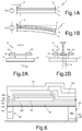
- a cantilever beam 1 is illustrated, constrained at a first end 2 and free to bend at a second end 3.
- the beam 1 is here formed by a stack of layers including a supporting layer 5, for example of a semiconductor material of a first conductivity type, here a P type, an active layer 6for example of intrinsic (non-doped) semiconductor material, forming a piezoelectric layer, and a top layer 7, for example of a semiconductor material of a second conductivity type, here an N type.
- the optical device designated by 10
- the optical device comprises a membrane 15, of glass, resting, through a lens element 11 of polymeric material, on a support 12, also of glass, and carrying two piezoelectric regions 13, arranged at a distance from each other.
- the membrane 15 and the lens element 11 have a planar surface and do not modify the path of a light beam 16 that traverses them.
- the piezoelectric regions 13 are biased, they cause a deformation of the membrane 15.
- the deformation of the central area of the membrane 15 is transmitted to the lens element 11, the top surface whereof curves, modifying the focus of the lens element 11 and thus the path of the light beam 16. It is thus possible to modify the optical transmission characteristics of the device 10.
- the strain generated by biasing a piezoelectric layer causes a deformation in a vertical direction, perpendicular to the extension plane of the piezoelectric layer.
- US 2007/0024715 discloses a piezoelectric actuator movable in the plane of the beam by virtue of a reinforcing member having a flexural rigidity in the width direction I slower than in the thickness direction.
- the aim of the present invention is to provide a MEMS actuator operating according to the piezoelectric principle and acting in the plane.
- a MEMS actuator device is provided, as defined in the attached claims.
- the present MEMS actuator comprises a beam carrying a piezoelectric region and having a first end constrained to a substrate and a second end connected to a Z-constraint structure, with a hinge structure arranged between the beam and the Z-constraint structure .
- the Z-constraint structure prevents or substantially reduces deflection of the second end of the beam in a vertical direction, but allows the second end to displace in the plane when the beam undergoes deformation by the piezoelectric effect.
- the Z-constraint structure causes the displacement in a vertical direction to be less than 5% with respect to the displacement in the plane.
- a lever structure fixed with respect to the second end of the beam and pivoted at the Z-constraint structure amplifies the in-plane movement of the latter.
- the in-plane movement may be further amplified by similar piezoelectric units, generating an in-plane movement of the actuator with a desired amplitude.
- Figures 3 and 4 show an embodiment of an actuator 100 made using the MEMS technology, operating according to a piezoelectric principle and mobile in the plane.
- the actuator 100 comprises a monolithic region 121 of semiconductor material, for example mono- or polycrystalline silicon, obtained, for example, by epitaxial growth on a sacrificial layer and defined via usual photolithographic masking and chemical etching steps so as to form a plurality of units 22, which are connected in series to each other and are monolithic with respect to each other.
- a monolithic region 121 of semiconductor material for example mono- or polycrystalline silicon, obtained, for example, by epitaxial growth on a sacrificial layer and defined via usual photolithographic masking and chemical etching steps so as to form a plurality of units 22, which are connected in series to each other and are monolithic with respect to each other.
- the units 22 comprise a base unit 22A, a first lateral unit 22B and a second lateral unit 22C, arranged on one side of the base unit 22A and connected to the latter, in series, as explained hereinafter. Possible other lateral units may be connected in series to the second lateral unit 22C, if so desired. Furthermore, other lateral units may be provided on the opposite side of the base unit 22A, in this case the base unit 22A having longitudinal symmetry.
- the units 22 are formed by elongated elements that extend parallel or transverse to each other (for example, perpendicular to each other). Even though, when actuated, some elements of the units 22 undergo deformation, rotate, or translate with respect to the rest position, as described hereinafter with reference to Figures 7-10 , the following description refers to the rest condition illustrated in Figures 3 and 4 .
- the base unit 22A is substantially formed by a base beam 20, by a first pillar 23 and a second pillar 24, by a constrained arm 31 and by a base hinge structure 25, the constrained arm 31 and the base hinge structure 25 forming a base constraint structure 21.
- the base unit 22A further comprises a base lever arm 33, pivoted on the base constraint structure 21.
- the base beam 20 has a main extension (length) parallel to an axis Y of a Cartesian reference system XYZ, and has a first end 20A and a second end 20B.
- the first end 20A of the base beam 20 is constrained to a substrate 28, for example of monocrystalline silicon, by the first pillar 23, which extends transversely to the base beam 20, parallel to the axis Z of the Cartesian reference system XYZ.
- the first pillar 23 extends between the first end 20A of the base beam 20 and the substrate 28, and is rigid with them.
- the second pillar 24 extends from the second end 20B of the base beam 20 to the substrate 28, also extends parallel to the axis Z, without being constrained to the substrate 28.
- the second pillar 24 has a height (in direction Z) that is slightly lower than the first pillar 23; for example, it is formed on a sacrificial portion of smaller depth, removed when releasing the monolithic region 121, as explained hereinafter.
- the first and second pillars 23, 24 could have the same thickness, and the substrate could be removed underneath the second pillar 24.
- the base beam 20 may have a thickness (in direction Z) of 3-20 ⁇ m, a length (in direction Y) of approximately 200-1000 ⁇ m, and a width (in direction X) of 40-100 ⁇ m, the first pillar 23 could have a height of approximately 50-400 ⁇ m, and the second pillar 24 could have a height of approximately 40-350 ⁇ m.
- the first piezoelectric strip 29 may have an extension (width and length) slightly smaller than the area of the base beam 20.
- the constrained arm 31 is formed by a vertical wall extending parallel to the base beam 20 and has a constrained end 31A close to the second end 20B of the base beam 20, to which it is connected through the base hinge structure 25.
- the constrained arm 31 is here anchored to the substrate 28 throughout its length (in direction Y), which is approximately one half that of the base beam 20, and has the same height as the first pillar 23.
- the constrained arm 31 has a smaller width than the base beam 20, for example 10-50 ⁇ m (in general, its width depends upon the desired stiffness of the structure).
- the base hinge structure 25 comprises a first hinge portion 26 and a second hinge portion 27, formed by smaller thickness portions, connecting the base beam 20 to the constrained arm 31 and to the base lever arm 33.
- the first hinge portion 26 of the base hinge structure 25 extends between the second end 20B of the base beam 20 and the base lever arm 33, of which it represents an ideal prolongation, of smaller width (in direction Y).
- the first hinge portion 26 may have a width of 10-50 ⁇ m (in general, its width depends upon the desired stiffness of the structure).
- the second hinge portion 27 of the base hinge structure 25 extends between the base lever arm 33 and the constrained arm 31, of which it represents an ideal prolongation, of a smaller width (in direction X).
- the base lever arm 33 has a main extension perpendicular to the base beam 20, and thus parallel to axis X, and is formed by a wall having a height (parallel to axis Z) equal the second pillar 24.
- Both hinge portions 26, 27 have a height (in direction Z) that is the same as the second pillar 24 and the base lever arm 33.
- the constrained arm 31, the base lever arm 33, and the base hinge structure 25, which are substantially rigid along Z due to their thickness, prevent (to a first approximation) the second end 20B of the base beam 20 from bending vertically.
- the base hinge structure 25 allows the second end 20B of the base beam 20 to move in the plane XY and forms a fulcrum for the base lever arm 33, which may thus rotate in plane XY.
- the base lever arm 33 Since the base lever arm 33 is articulated in proximity of an end thereof (connected to the second end 20B of the base beam 20) and has its longer portion between the base hinge structure 25 (fulcrum) and the other end, it amplifies the movement of displacement/rotation of the second end 20B of the base beam 20, as illustrated in Figure 5 .
- the base unit 22A is connected to the first lateral unit 22B through a first connection arm 36.
- the first connection arm 36 extends parallel to the base beam 20 and to the constrained arm 31, has a length (in direction Y) equal the base beam 20, a height (in direction Z) equal to the second pillar 24, and a width (in direction X) of 100-500 ⁇ m. Furthermore, it has a first end rigidly connected to the base lever arm 33 and a second end rigidly connected to the first lateral unit 22B.
- the first lateral unit 22B in turn comprises a first lateral beam 40 and a first lateral constraint structure 41.
- the first lateral unit 22B further comprises a first lateral lever arm 42 and a second lateral lever arm 43.
- the first lateral unit 22B has a longitudinally symmetrical structure, wherein each half is similar to the base unit 22A, but turned over through 180°. The elements of the first lateral unit 22B similar to those of the base unit 22A are thus identified by the same reference numbers increased by 20.
- the first lateral beam 40 is here altogether similar to the base beam 20 and has in particular the same length, the same width, and the same thickness. It extends parallel to the base beam 20 and carries a second piezoelectric strip 49, here identical to the first piezoelectric strip 29, and thus of the same material and having the same geometrical characteristics.
- the first lateral beam 40 has a first end 40A rigidly connected to the first lateral constraint structure 41 and a second end 40B articulated to the first lateral constraint structure 41 and to the first and second lateral lever arms 42, 43.
- a lateral pillar portion 48 extends from the second end 40B of the first lateral beam 40 to the substrate 28, in a direction parallel to the axis Z, without being constrained to the substrate 28 itself, like the second pillar 24.
- the lateral pillar portion 48 here has a height (in the direction Z) substantially equal to that of the second pillar 24.
- the first lateral constraint structure 41 comprises a U-shaped element 50, a first lateral hinge structure 44, and a second lateral hinge structure 45.
- the U-shaped element 50 in turn comprises a base side 51 extending perpendicular to the first lateral beam 40, and two lateral constrained arms 52, 53, each extending on a respective side of the first lateral beam 40, parallel to the latter and at the same distance therefrom.
- the base side 51 is fixed with respect to the first end 40A of the first lateral beam 40 and is arranged so that the first lateral beam 40 extends exactly at the centre of and longitudinally with respect to the first lateral constraint structure 41, with the lateral constrained arms 52, 53 arranged (at rest) symmetrically on the two longitudinal sides of the first lateral beam 40.
- the lateral constrained arms 52, 53 of the first lateral constraint structure 41 have a length (in direction Y) approximately equal to the first lateral beam 40 and are connected (at their ends remote from the base side 51) to the second end 40B of the first lateral beam 40 through the first and second lateral hinge structures 44, 45.
- the base side 51 and the two lateral constrained arms 52, 53 of the first lateral constraint structure 41 have a width approximately equal to the first connection arm 36 and have a depth (in direction Z) equal to the first connection arm 36, as may be noted in particular in Figure 3 for the lateral constrained arm 52.
- the first lateral constraint structure 41 is thus substantially rigid (undeformable) in direction Z.
- the first and second lateral hinge structures 44, 45 are similar to the base hinge structure 25 and are each formed by a respective first lateral hinge portion 46 and second lateral hinge portion 47, formed by smaller width regions.
- the first lateral hinge portion 46 of the first lateral hinge structure 44 extends as a prolongation of the first lateral lever arm 42, between the latter and the second end 40B of the first lateral beam 40 (and is thus contiguous to the lateral pillar portion 48).
- the second lateral hinge portion 47 of the first lateral hinge structure 44 extends as a prolongation of the first lateral constrained arm 52, between the latter and the second lateral lever arm 42.
- the first lateral hinge portion 46 of the second lateral hinge structure 45 extends as a prolongation of the second lateral lever arm 43, between the latter and the second end 40B of the first lateral beam 40 (and is thus contiguous to the lateral pillar portion 48).
- the second lateral hinge portion 47 of the second lateral hinge structure 45 extends as a prolongation of the second lateral constrained arm 53, between the latter and the second lateral lever arm 43.
- the first lateral constraint structure 41 prevents, to a first approximation, vertical displacement (in direction Z) of the second end 40B of the first lateral beam 40; shrinking and deformation of the latter, when biased, cause in-plane rotation of the lateral articulated arms 42, 43, about a substantially vertical axis, as explained hereinafter with reference to Figures 7-10 .
- the second lateral lever arm 43 is connected to the second lateral unit 22C through a second connection arm 56, altogether similar to the first connection arm 36. It thus extends (at rest) parallel to the base beam 20, has a length equal to the latter, and a height equal to the second pillar 24.
- the second connection arm 56 further has a first end rigidly connected to the second lateral lever arm 43 and a second end rigidly connected to the second lateral unit 22C.
- the second lateral unit 22C is altogether identical to the first lateral unit 22B, but it is turned over through 180°. Thus, its elements are identified by the same reference numbers increased by 20.
- the second lateral unit 22C comprises a second lateral beam 60, a second lateral constraint structure 61, a third lateral lever arm 62 and a fourth lateral lever arm 63.
- the second lateral constraint structure 61 comprises a U-shaped element 70 (including lateral constrained arms 72, 73), a third lateral hinge structure 64, and a fourth lateral hinge structure 65, which have the same mutual arrangement and the same geometrical characteristics as those already described for the corresponding components 40-43, 52, 53 of the first lateral unit 22B.
- the second lateral beam 60 carries a third piezoelectric strip 69, here altogether identical to the first and second piezoelectric strips 29, 49.
- the second lateral lever arm 63 of the second lateral unit 22C is connected to a third connection arm 76, identical to the first and second connection arms 36, 56. It may be connected to other lateral units (not illustrated) to further amplify the actuation movement or simply to form an actuation end, which may be connected to a driven member (not illustrated), as explained hereinafter.
- the second lateral unit 22C is turned over with respect to the first lateral unit 22B, the second end 40B of the first lateral beam 40 and the first end 60A of the second lateral beam 60 are aligned to the first end 20A of the base beam 20, and the first end 40A of the first lateral beam 40 and the second end 60B of the second lateral beam 60 are aligned to the second end of the base beam 20.
- the beam 20 is formed by a supporting layer 180 of epitaxially grown silicon, covered at the bottom by a bottom insulating layer 181 and at the top by a top insulating layer 182, for example, both of thermally grown silicon oxide.
- a stack on the top insulating layer 182 is formed by a bottom electrode 183, of electrically conductive material, for example titanium (Ti) or platinum (Pt); a piezoelectric material 191; a top electrode 184, for example of TiW; a first dielectric layer 185 and a second dielectric layer 186, for example of CVD (Chemical Vapour Deposition) deposited silicon oxide and silicon nitride; a contact line 189 of conductive material, for example aluminium and/or copper; and a passivation layer 190, for example silicon oxide and/or CVD deposited nitride.
- CVD Chemical Vapour Deposition
- Figure 6 also shows the structure of the first pillar 23, which, in the illustrated embodiment, comprises a first silicon portion 192' and a second silicon portion 193 bonded together, and the structure of the second pillar 24, formed by a single silicon portion 192", formed simultaneously with and with the same thickness as the first silicon portion 192' of the first pillar 23, for example as explained hereinafter.
- first pillar 23 may have a broad area, with portions not illustrated, for forming pads and possible other structures necessary for the electrical connections with the electrodes 183, 184, as to for a person skilled in the art.
- the structure of the lateral beams 40, 60 is similar, and differs only in that, instead of the pillar 23, they have lateral pillar portion 48 or the base side 51, made like the second pillar 24.
- the actuator 100 may be formed by bonding two wafers, worked separately and bonded together according to the manufacturing method described hereinafter.
- a first wafer comprising the substrate 28 is processed by growing a sacrificial layer, for example of thermal oxide having a thickness of 2-10 ⁇ m, on the substrate 28; first masking and etching to define through openings in the sacrificial layer where the first pillars 23 and the constrained arms 31 are to be grown; epitaxial growing polysilicon with a thickness of, for example, 5-20 pm; and lapping and removing the epitaxial polysilicon until reaching the sacrificial layer so as to leave only the polysilicon portions in the through openings defined previously, thus forming the second portion 193 of the first pillars 23 (and of the constrained arms 31).
- a sacrificial layer for example of thermal oxide having a thickness of 2-10 ⁇ m
- a second wafer is processed; the second wafer being for example a SOI (Silicon-On-Insulator) type with a thickness of 400-720 ⁇ m, in which the intermediate oxide layer has a thickness of 0.5-1 ⁇ m and is intended to form the bottom insulating layer 181 of Figure 6 , one of the two silicon layers (for example, the top one) forms the supporting layer 180 of Figure 6 , and the other silicon layer (in the example, the bottom one) forms the portions 192' and 192" of Figure 6 .
- the intermediate oxide layer (bottom insulating layer 181) has a stress-balancing function and operates also as a hard stop while etching the bottom silicon layer for forming portions 192', 192", as explained hereinafter.
- the second wafer is processed by thermally growing the top insulating layer 182 on the top silicon layer (supporting layer 180); depositing and patterning the layers intended to form the piezoelectric regions and the corresponding biasing and electrical-connection structures, as well as the dielectric layers (regions 183, 184, 185, 186, 190 and 191 of Figure 6 ), in a per se known manner; lapping the back of the second wafer until reaching the desired thickness for the pillars 24, 48, the lever arms 33, 42, 43 and the hinge structures 25, 44, 45, 64, 65 in the bottom silicon layer; masking and back-etching the bottom silicon layer to define the structure of the beams 20, 40, and 60, until reaching the bottom insulating layer 181 of Figure 6 (in practice, openings are provided having a shape in plan view corresponding to that of the beams 20, 40, 60).
- the two wafers are bonded by aligning the portions 193 of the first wafer with the corresponding portions (not yet defined) in the bottom silicon layer of the second wafer.
- the geometry of Figure 4 is defined and the top silicon layer is etched as far as the bottom insulating layer 181; the bottom insulating layer 181 and then the sacrificial oxide layer of the first wafer are removed to release the entire monolithic structure 121 except for the pillars 23 and the constrained arms 31 that remain fixed to the substrate 28.
- the actuator 100 is in its rest configuration, illustrated in Figures 3-5 and in Figures 7 and 8 with a solid line.
- the piezoelectric material strips 29, 49, 69 are biased through the electrodes 183, 184 of Figure 6 , for example by applying a voltage of 30-40 V to the top electrode 184 and grounding the bottom electrode 183, they shrink, causing a deformation of the respective beams 20, 40, 60.
- Figure 7 shows in side view, with a dashed line and in an exaggerated way, for sake of clarity, the deformation of the base beam 20 while biasing the corresponding piezoelectric strip 29.
- deformation of the base beam 20 substantially consists in a contraction or shrinking thereof, with displacement and rotation in the plane XY of the second end 20B of the base beam 20 (see, in particular, the top plan view of Figure 8 ).
- the first end 20A of the base beam 20 is constrained to the substrate 28 through the first pillar 23 (and thus, to a first approximation, does not have any degree of freedom).
- the second end 20B is constrained in direction Z by the constrained arm 31 (and thus may not freely deflect towards the substrate 28), but may move in the plane XY, since the second pillar 24 is not constrained to the substrate 28 and due to the presence of the base hinge structure 25, which provides (to a first approximation) an (angular) degree of freedom in the plane XY.
- shrinking of the base beam 20 generates a force (as represented in an exaggerated way with a dashed line in Figure 7 and indicated by the arrow A in Figures 5 , 7, and 8 ) that "pulls" the second end 20B of the base beam 20 towards the first end 20A, causing rotation thereof in a counterclockwise direction (as represented in Figures 5 and 8 with a dashed line and indicated by the arrow B) due to the base constraint structure 21.
- Rotation of the second end 20B causes a corresponding rotation of the base lever arm 33, which also rotates in the plane XY, amplifying the movement (arrow B' of Figure 8 ).
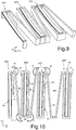
- Rotation of the base lever arm 33 is transferred to the first lateral unit 22B through the first connection arm 36, fixed with respect to the base lever arm 33 and to the first lateral lever arm 42, as illustrated in Figures 9, 10 .
- Simultaneous biasing of the first and second lateral units 22B, 22C causes similar deformations and displacements thereof and, as a whole, movement of the lateral unit 22A, 22C away from the base unit 22A, in "concertina” fashion.
- shrinking of the piezoelectric material strips 49, 69 causes shortening in direction Y and deformation of the corresponding lateral beams 40, 60, with a mechanism similar to the one described for the base beam 20.
- the second ends 40B and 60B of the lateral beams 40, 60 may not displace in direction X; translation in direction Y of the second ends 40B and 60B, however, causes a "pull" action on the lateral lever arms 42, 43 and 62, 63 and thus rotation thereof in the plane XY, as represented in Figure 10 by arrows C, C', D and D'.
- rotation of the first lateral lever arm 42 (arrow C) is concordant with the rotation, indicated by arrow B, of the lever arm 33 of the base unit 22A (transmitted through the first connection arm 36) and, to a first approximation, of the same amount.
- This causes the first lateral beam 40 to rotate (with respect to the first lateral lever arm 42) through an angle equal and opposite to that of the rotation transmitted by the first connection arm 36. Consequently, to a first approximation, the two rotations cancel out, and the first lateral beam 40 does not rotate with respect to the Cartesian reference system XYZ, but shifts laterally in direction X, away from the base unit 22A.
- rotation of the second lever arm 43 of the first lateral unit 22B causes rotation in a clockwise direction of the second connection arm 56 and of the first lever arm 63 of the second lateral unit 22C.
- the second lateral beam 60 rotates in a direction opposite to the first lever arm 63 of the second lateral unit 22C; thus, the two rotations cancel out, and the second lateral beam 60 undergoes only, to a first approximation, a displacement in direction X, without rotating.
- the displacement in direction X generated by the first lateral unit 22A is thus amplified by the second lateral unit 22B.
- Each possible lateral unit may amplify the movement in direction X.
- the last unit of the series designated by 22N in Figure 10 , may comprise an actuation element 95 directly connected to one of the ends of the n-th lateral beam 80 so that its displacement is, to a first approximation, oriented only in direction X (as indicated by arrow E).
- Other solutions are, however, possible.
- the second end 20B of the base beam 20 essentially moves in the plane XY, converting the strains generated by the piezoelectric effect, and directed according to axis Z, into a in-plane movement.
- the base lever arm 33 and the lateral units 22B, 22C, ..., 22N amplify this in-plane movement to obtain a greater actuation amplitude, substantially in a direction perpendicular to the longitudinal extensions of the units 22.
- An actuated member of an electronic device may thus be connected to the actuation element 95.
- the actuation member 95 may be connected to a liquid-jet printing head, an autofocus system, a micro-pump, a microswitch, an optical-fibre aligner, an atomic-force microscope for measurements of surface roughness, a hard-disk device, a precision surgical instrument, a precision positioning device, etc.
- Figure 11 shows an embodiment of a rotary actuator 200, comprising a plurality of units 122A, 122B, 122C, ..., oriented in the same way, i.e., with the hinge structures 125, 144, 145, 164, 165 aligned to each other (in a rest condition of the actuator 200).
- a rotary actuator 200 comprising a plurality of units 122A, 122B, 122C, ..., oriented in the same way, i.e., with the hinge structures 125, 144, 145, 164, 165 aligned to each other (in a rest condition of the actuator 200).
- all the units 122A, 122B, ..., 122N rotate in a same direction (here counterclockwise), so that it is possible to obtain an amplified rotation movement.
- the lateral units 222B, 222C may be arranged at 180° with respect to the base unit 222A, so as to obtain a roto-translation (a movement similar to that of the hinges of cabinet doors that are able to rotate and extend).
- the base unit 22A could be formed like the lateral units 22B, 22C, or exactly like one half thereof, with the difference that the first end 20A of the base beam 20 is in any case anchored to the substrate 28 through the first pillar 23 for supporting the monolithic region 121.
- the constrained arm 31 might not be anchored to the substrate 28 and extend throughout the length of the base beam 20, parallel thereto, with a first end articulated to the second end 20B of the base beam 20 (as illustrated in the figures) and a second end connected to the first end 20A of the base beam 20, as in the lateral units 22A, 22B for the lateral constrained arms 52, 53.
- the constrained arm 31 could be anchored to the substrate 28, and extend throughout the length of the base beam 20, parallel thereto, in the way described above.
- the constrained arm 31 could be formed by a simple column anchored to the substrate 2.
- the piezoelectric strips may be of a different material, for example of AlN or KNN (sodium potassium niobate-(K, Na) NbO 3 ) .
- the base unit 22A may also be anchored laterally, forming the first end 20A of the base beam 20 protruding from a frame fixed with respect to the substrate 28 and surrounding the monolithic region 121.
Landscapes
- Engineering & Computer Science (AREA)
- Power Engineering (AREA)
- Microelectronics & Electronic Packaging (AREA)
- Physics & Mathematics (AREA)
- Computer Hardware Design (AREA)
- Chemical & Material Sciences (AREA)
- Analytical Chemistry (AREA)
- General Physics & Mathematics (AREA)
- Optics & Photonics (AREA)
- Micromachines (AREA)
- General Electrical Machinery Utilizing Piezoelectricity, Electrostriction Or Magnetostriction (AREA)
Claims (19)
- MEMS-Aktuatorvorrichtung (100; 200) eines piezoelektrischen Typs, umfassend ein Substrat (28) und eine Basiseinheit (22A; 122A), wobei die Basiseinheit aufweist:ein Basisträgerelement (20) mit einem ersten Ende (20A), einem zweiten Ende (20B), einer Haupterstreckung in einer Erstreckungsebene und einer Dicke in einer Dickenrichtung senkrecht zur Erstreckungsebene, die kleiner als die Haupterstreckung ist;einen piezoelektrischen Bereich (29) an oder in dem Trägerelement;einen Ankerbereich (23), der bezüglich des Basisträgerelements und des Substrats (28) fixiert ist; undeine Basisbeschränkungsstruktur (21), die mit dem zweiten Ende des Basisträgerelements (20) verbunden ist, wobei die Beschränkungsstruktur derart konfiguriert ist, dass sie im Wesentlichen eine Bewegung des zweiten Endes des Basisträgerelements in der Erstreckungsebene ermöglicht und eine Verformung des Basisträgerelements in der Dickenrichtung verhindert oder wesentlich verringert,wobei die Basisbeschränkungsstruktur ein Basisbeschränkungselement (31), das in der Dickenrichtung nicht verformbar ist, und eine Basisscharnierstruktur (25; 125), die zwischen dem Basisträgerelement (20) und dem Basisbeschränkungselement (31) angeordnet ist, umfasst.
- Vorrichtung nach Anspruch 1, wobei das Basisbeschränkungselement (31) eine Dicke aufweist, die größer als das Basisträgerelement (20) ist.
- Vorrichtung nach Anspruch 1, wobei sich der Ankerbereich (23) zwischen dem ersten Ende des Basisträgerelements (20) und dem Substrat (28) erstreckt und das Basisbeschränkungselement (31) eine Wand umfasst, die sich parallel zu dem Basisträgerelement erstreckt und an dem Substrat (28) verankert ist.
- Vorrichtung nach einem der vorhergehenden Ansprüche, wobei die Basisscharnierstruktur (25) einen Scharnierbereich (26, 27) umfasst, der mit dem zweiten Ende des Basisträgerelements (20) und mit dem Basisbeschränkungselement (31) verbunden ist, wobei der Scharnierbereich eine kleinere Breite als das Basisträgerelement und das Beschränkungselement und eine Dicke in der Dickenrichtung größer als das Basisträgerelement (20) aufweist.
- Vorrichtung nach einem der vorhergehenden Ansprüche, wobei die Basiseinheit (22A) über die Basisscharnierstruktur (25) mit einer ersten lateralen Einheit (22B) verbunden ist, wobei die erste laterale Einheit (22B) durch ein erstes laterales Trägerelement (40) und eine erste laterale Beschränkungsstruktur (41) gebildet wird, wobei das erste laterale Trägerelement (40) eine Haupterstreckung in der Erstreckungsebene, eine Dicke in der Dickenrichtung, die kleiner als ihre Haupterstreckung ist, ein jeweiliges erstes Ende (40A) und ein jeweiliges zweites Ende (40B) aufweist, und einen jeweiligen piezoelektrischen Bereich (49) trägt, wobei die erste laterale Beschränkungsstruktur (22B) starr mit dem ersten Ende (40A) des ersten lateralen Trägerelements (40) ist und an dem zweiten Ende (40B) des ersten lateralen Trägerelements gelenkig angebracht ist, wobei die erste laterale Beschränkungsstruktur (41) derart konfiguriert ist, dass sie im Wesentlichen eine Verformung des ersten lateralen Trägerelements in der Erstreckungsebene ermöglicht und eine Verformung des ersten lateralen Trägerelements in Dickenrichtung verhindert oder wesentlich verringert.
- Vorrichtung nach Anspruch 5, wobei die Basiseinheit (22A) mit der ersten lateralen Einheit (22B) über einen Basishebelarm (33) verbunden ist, der mit der Basisscharnierstruktur (25) und mit der ersten lateralen Beschränkungsstruktur (41) verbunden ist.
- Vorrichtung nach Anspruch 6, wobei sich das erste laterale Trägerelement (40), in Ruhe, parallel zu dem Basisträgerelement (20) erstreckt, und sich der Basishebelarm (33), in Ruhe, senkrecht zu dem Basisträgerelement (20) erstreckt.
- Vorrichtung nach Anspruch 7, wobei die Basisscharnierstruktur (25; 125) ein erstes Basisscharnierelement (26), das zwischen dem zweiten Ende des Basisträgerelements (20) und einem Ende des Basishebelarms (33) angeordnet ist, und ein zweites Basisscharnierelement (27), das zwischen dem Ende des Basishebelarms (33) und der Basisbeschränkungsstruktur (31) angeordnet ist, umfasst, wobei das erste und das zweite Basisscharnierelement (26, 27) jeweilige Dicken in der Dickenrichtung größer als das Basisträgerelement (20) und eine Breite in der Erstreckungsebene kleiner als das Basisträgerelement und der Basishebelarm (33) aufweisen.
- Vorrichtung nach einem der Ansprüche 6 bis 8, wobei die erste laterale Einheit (22B) einen ersten lateralen Hebelarm (42), der mit dem zweiten Ende (40B) des ersten lateralen Trägerelements (40) gekoppelt ist und mit dem Basishebelarm (33) verbunden ist, umfasst.
- Vorrichtung nach Anspruch 9, wobei die erste laterale Beschränkungsstruktur (41) einen ersten lateralen Beschränkungsarm (52) und eine erste laterale Scharnierstruktur (44) umfasst, wobei sich der erste laterale Beschränkungsarm (52), in Ruhe, parallel zu und in einem Abstand von dem ersten lateralen Trägerelement (40) erstreckt und ein erstes Ende, das mit dem ersten Ende (40A) des ersten lateralen Trägerelements (40) starr verbunden ist, und ein zweites Ende, das über die erste laterale Scharnierstruktur (44) mit dem zweiten Ende (40B) des ersten lateralen Trägerelements (40) verbunden ist, aufweist.
- Vorrichtung nach dem vorhergehenden Anspruch, wobei die erste laterale Scharnierstruktur (44) ein erstes laterales Scharnierelement (46), das zwischen dem zweiten Ende (40B) des ersten lateralen Trägerelements (40) und dem ersten lateralen Hebelarm (42) angeordnet ist, und ein zweites laterales Scharnierelement (47), das zwischen dem ersten lateralen Hebelarm (42) und dem zweiten Ende des ersten lateralen Beschränkungsarms (52) angeordnet ist, umfasst, wobei das erste und das zweite laterale Scharnierelement (44, 45) jeweilige Dicken in der Dickenrichtung größer als das erste laterale Trägerelement (40) und eine Breite in der Erstreckungsebene kleiner als der erste laterale Hebelarm (42) und der erste laterale Beschränkungsarm (52) aufweisen.
- Vorrichtung nach einem der Ansprüche 9 bis 11, wobei die erste laterale Einheit (22B) einen zweiten lateralen Hebelarm (43) umfasst, der mit dem zweiten Ende (40B) des zweiten lateralen Trägerelements (40) an einer dem ersten lateralen Hebelarm (42) gegenüberliegenden Seite gekoppelt ist, und die erste laterale Beschränkungsstruktur (41) ferner einen zweiten lateralen Beschränkungsarm (53) und eine zweite laterale Scharnierstruktur (45) umfasst, wobei sich der zweite laterale Beschränkungsarm (53), in Ruhe, parallel und in einem Abstand von dem ersten lateralen Trägerelement (40) erstreckt und ein erstes Ende, das mit dem ersten Ende (40B) des ersten lateralen Trägerelements (40) starr verbunden ist, und eine zweites Ende, das über die zweite laterale Scharnierstruktur (45) mit dem zweiten Ende (40B) des ersten lateralen Trägerelements (40) verbunden ist, aufweist.
- Vorrichtung nach Anspruch 12, wobei die zweite laterale Scharnierstruktur (45) ein drittes laterales Scharnierelement (46), das zwischen dem zweiten Ende (40B) des ersten lateralen Trägerelements (40) und dem zweiten lateralen Hebelarm (43) angeordnet ist, und ein viertes laterales Scharnierelement (47), das zwischen dem zweiten lateralen Hebelarm (43) und dem zweiten Ende des ersten lateralen Beschränkungsarms (53) angeordnet ist, umfasst, wobei das dritte und vierte laterale Scharnierelement (46, 47) jeweilige Dicken größer als das erste laterale Trägerelement (40) und eine Breite in der Erstreckungsebene kleiner als der zweite laterale Hebelarm (43) und der zweite laterale Beschränkungsarm (53) aufweisen.
- Vorrichtung nach Anspruch 12 oder 13, wobei die erste laterale Einheit (22B) über den zweiten lateralen Hebelarm (43) mit einer zweiten lateralen Einheit (22C) verbunden ist, wobei die zweite laterale Einheit (22C) durch ein zweites laterales Trägerelement (60) und eine zweite laterale Beschränkungsstruktur (61) gebildet ist, wobei das zweite laterale Trägerelement (60) eine Haupterstreckung in der Erstreckungsebene, eine Dicke in der Dickenrichtung, ein jeweiliges erstes Ende (60A) und ein jeweiliges zweites Ende (60B) aufweist und einen jeweiligen piezoelektrischen Bereich (69) trägt, wobei die zweite laterale Beschränkungsstruktur (61) bezüglich des ersten Endes (60A) des zweiten lateralen Trägerelements (60) fixiert und an dem zweiten Ende (60B) des zweiten lateralen Trägerelements und der ersten lateralen Einheit (22B) angelenkt ist, wobei die zweite laterale Beschränkungsstruktur (61) derart konfiguriert ist, dass sie im Wesentlichen eine Verformung des zweiten lateralen Trägerelements (60) in der Erstreckungsebene ermöglicht und eine Verformung des zweiten lateralen Trägerelements (60) in Dickenrichtung verhindert oder wesentlich reduziert.
- Vorrichtung nach einem der Ansprüche 9 bis 14, ferner umfassend einen ersten Verbindungsarm (36), der mit dem Basishebelarm (33) und dem ersten lateralen Hebelarm (42) starr verbunden ist; wobei sich der erste laterale Hebelarm, in Ruhe, parallel und in einem Abstand von dem Basishebelarm (33) erstreckt, und sich der erste Verbindungsarm (36), in Ruhe, quer zu dem Basishebelarm (33) und zu dem ersten lateralen Hebelarm (42) zwischen der Basiseinheit (22A) und der ersten lateralen Einheit (22B) erstreckt.
- Vorrichtung nach Anspruch 14, wobei die zweite laterale Einheit (22C) einen dritten lateralen Hebelarm (62) umfasst, der an dem zweiten Ende (60B) des zweiten lateralen Trägerelements (60) angelenkt ist, wobei die Vorrichtung ferner einen zweiten Verbindungsarm (56) umfasst, der sich, in Ruhe, parallel zu dem ersten und zweiten lateralen Trägerelement (40, 60) erstreckt, wobei der zweite Verbindungsarm (56) bezüglich dem zweiten lateralen Hebelarm (43) und dem dritten lateralen Hebelarm (62) fixiert ist und sich zwischen dem ersten und dem zweiten lateralen Trägerelement (40, 60) erstreckt.
- Vorrichtung nach Anspruch 14, wobei, in Ruhe, das erste Ende (40A) des ersten lateralen Trägerelements (40) und das erste Ende (60A) des zweiten lateralen Trägerelements (60) in Bezug zueinander ausgerichtet sind und das zweite Ende (40B) des ersten lateralen Trägerelements (40) und das zweite Ende (60B) des zweiten lateralen Trägerelements (60) in Bezug zueinander ausgerichtet sind.
- Vorrichtung nach Anspruch 17, wobei der Basishebelarm (33) und der erste laterale Hebelarm (42) sich aneinander entlang erstrecken und zueinander starr sind, und der zweite laterale Hebelarm (43) an der zweiten lateralen Beschränkungsstruktur (61) der zweiten lateralen Einheit (22C) angelenkt ist.
- Vorrichtung nach Anspruch 14, wobei die Basiseinheit (22A) und die erste und zweite laterale Einheit (22B, 22C) in derselben monolithischen Schicht (21) aus Halbleitermaterial gebildet sind.
Applications Claiming Priority (1)
| Application Number | Priority Date | Filing Date | Title |
|---|---|---|---|
| IT102016000132144A IT201600132144A1 (it) | 2016-12-29 | 2016-12-29 | Dispositivo attuatore micro-elettro-meccanico con comando piezoelettrico, mobile nel piano |
Publications (2)
| Publication Number | Publication Date |
|---|---|
| EP3343653A1 EP3343653A1 (de) | 2018-07-04 |
| EP3343653B1 true EP3343653B1 (de) | 2020-07-29 |
Family
ID=58609916
Family Applications (1)
| Application Number | Title | Priority Date | Filing Date |
|---|---|---|---|
| EP17177446.6A Active EP3343653B1 (de) | 2016-12-29 | 2017-06-22 | Auf der ebene verschiebbare piezoelektrische mikroelektromechanische aktuatorvorrichtung |
Country Status (4)
| Country | Link |
|---|---|
| US (1) | US10770643B2 (de) |
| EP (1) | EP3343653B1 (de) |
| CN (2) | CN207891042U (de) |
| IT (1) | IT201600132144A1 (de) |
Families Citing this family (7)
| Publication number | Priority date | Publication date | Assignee | Title |
|---|---|---|---|---|
| IT201600132144A1 (it) | 2016-12-29 | 2018-06-29 | St Microelectronics Srl | Dispositivo attuatore micro-elettro-meccanico con comando piezoelettrico, mobile nel piano |
| IT201800002364A1 (it) | 2018-02-02 | 2019-08-02 | St Microelectronics Srl | Dispositivo micro-manipolatore micro-elettro-meccanico con comando piezoelettrico, mobile nel piano |
| US11696507B2 (en) | 2018-12-14 | 2023-07-04 | Stmicroelectronics S.R.L. | Piezoelectric MEMS device with a suspended membrane having high mechanical shock resistance and manufacturing process thereof |
| CN113620232B (zh) * | 2020-05-07 | 2026-01-06 | 意法半导体股份有限公司 | 有改善机械属性的可变形结构的压电致动器及其制造方法 |
| IT202000010264A1 (it) * | 2020-05-07 | 2021-11-07 | St Microelectronics Srl | Attuatore piezoelettrico avente un sensore di deformazione e relativo procedimento di fabbricazione |
| IT202000010261A1 (it) | 2020-05-07 | 2021-11-07 | St Microelectronics Srl | Attuatore piezoelettrico dotato di una struttura deformabile avente migliorate proprieta' meccaniche e relativo procedimento di fabbricazione |
| JP2022189635A (ja) * | 2021-06-11 | 2022-12-22 | スタンレー電気株式会社 | Memsデバイス |
Family Cites Families (19)
| Publication number | Priority date | Publication date | Assignee | Title |
|---|---|---|---|---|
| US5046773A (en) | 1990-01-02 | 1991-09-10 | Hewlett-Packard Company | Micro-gripper assembly |
| JPH0890478A (ja) | 1994-09-29 | 1996-04-09 | Shimadzu Corp | マイクログリップ |
| DE19523229A1 (de) | 1995-06-27 | 1997-01-02 | Riad Dipl Ing Salim | Mikrogreifer für die Mikromontage |
| DE10107402A1 (de) | 2001-02-14 | 2002-08-29 | Ruben Keoschkerjan | Piezoelektrischer paralleler Mikrogreifer |
| KR100849155B1 (ko) * | 2003-11-20 | 2008-07-30 | 바이킹 테크놀러지스, 엘.씨. | 전기-기계식 액추에이터를 위한 통합적 열 보상 장치 및방법 |
| JP4799407B2 (ja) * | 2004-06-07 | 2011-10-26 | パナソニック株式会社 | アクチュエータ及び該アクチュエータを備えた微動機構並びに該微動機構を備えたカメラモジュール |
| US7876026B2 (en) * | 2008-08-21 | 2011-01-25 | The United States Of America As Represented By The Secretary Of The Army | Large force and displacement piezoelectric MEMS lateral actuation |
| FR2941533B1 (fr) * | 2009-01-23 | 2011-03-11 | Commissariat Energie Atomique | Capteur inertiel ou resonnant en technologie de surface, a detection hors plan par jauge de contrainte. |
| WO2010094102A1 (en) | 2009-02-17 | 2010-08-26 | Yu Sun | Device for grasping and active release of micro and nano objects |
| EP2317532A1 (de) * | 2009-10-28 | 2011-05-04 | Nxp B.V. | Piezoelektrische MEMS-Vorrichtung |
| DE102010021867A1 (de) * | 2010-05-28 | 2011-12-01 | Eurocopter Deutschland Gmbh | Kraftgenerator zur Anbringung an einer Struktur |
| JP5916577B2 (ja) * | 2012-09-26 | 2016-05-11 | 富士フイルム株式会社 | ミラー駆動装置及びその駆動方法 |
| CN104647347B (zh) | 2014-09-26 | 2016-08-24 | 浙江大学 | 基于柔性铰链放大的压电微夹钳 |
| FR3030474B1 (fr) * | 2014-12-23 | 2022-01-21 | Commissariat Energie Atomique | Dispositif de transformation d'un mouvement hors plan en un mouvement dans le plan et/ou inversement |
| CN205595376U (zh) * | 2015-04-30 | 2016-09-21 | 意法半导体股份有限公司 | 压电传感器 |
| CN105058366B (zh) | 2015-08-20 | 2017-03-22 | 宁波大学 | 一种四自由度压电微夹钳 |
| US10062832B2 (en) * | 2015-11-30 | 2018-08-28 | Sabic Global Technologies, B.V. | Methods and systems for making piezoelectric cantilever actuators |
| IT201600132144A1 (it) | 2016-12-29 | 2018-06-29 | St Microelectronics Srl | Dispositivo attuatore micro-elettro-meccanico con comando piezoelettrico, mobile nel piano |
| IT201800002364A1 (it) | 2018-02-02 | 2019-08-02 | St Microelectronics Srl | Dispositivo micro-manipolatore micro-elettro-meccanico con comando piezoelettrico, mobile nel piano |
-
2016
- 2016-12-29 IT IT102016000132144A patent/IT201600132144A1/it unknown
-
2017
- 2017-06-22 EP EP17177446.6A patent/EP3343653B1/de active Active
- 2017-06-27 CN CN201720762834.5U patent/CN207891042U/zh not_active Withdrawn - After Issue
- 2017-06-27 CN CN201710501989.8A patent/CN108249388B/zh active Active
- 2017-06-29 US US15/638,195 patent/US10770643B2/en active Active
Non-Patent Citations (1)
| Title |
|---|
| None * |
Also Published As
| Publication number | Publication date |
|---|---|
| EP3343653A1 (de) | 2018-07-04 |
| CN108249388A (zh) | 2018-07-06 |
| US10770643B2 (en) | 2020-09-08 |
| CN207891042U (zh) | 2018-09-21 |
| US20180190895A1 (en) | 2018-07-05 |
| IT201600132144A1 (it) | 2018-06-29 |
| CN108249388B (zh) | 2023-08-11 |
Similar Documents
| Publication | Publication Date | Title |
|---|---|---|
| EP3343653B1 (de) | Auf der ebene verschiebbare piezoelektrische mikroelektromechanische aktuatorvorrichtung | |
| EP3287830B1 (de) | Abtastendes mems-reflektorsystem | |
| US7876026B2 (en) | Large force and displacement piezoelectric MEMS lateral actuation | |
| US8724200B1 (en) | MEMS hierarchically-dimensioned optical mirrors and methods for manufacture thereof | |
| US8691099B2 (en) | Process for fabricating MEMS devices | |
| US8222796B2 (en) | Micro-electro-mechanical device with a piezoelectric actuator | |
| US11614634B2 (en) | Piezoelectric MEMS actuator for compensating unwanted movements and manufacturing process thereof | |
| CN209890247U (zh) | 压电型微机电致动器装置和便携式电子装置 | |
| US11427463B2 (en) | Piezoelectric MEMS device having a suspended diaphragm and manufacturing process thereof | |
| TWI605013B (zh) | 微光學機電掃描裝置與製造其之方法 | |
| US12185633B2 (en) | Piezoelectric mems device with a suspended membrane having high mechanical shock resistance and manufacturing process thereof | |
| EP3533569B1 (de) | Mikroelektromechanische mikromanipulationsvorrichtung mit auf der ebene beweglichem piezoelektrischem antrieb | |
| CN101279712B (zh) | 生成微机械结构的方法 | |
| US6556741B1 (en) | MEMS optical switch with torsional hinge and method of fabrication thereof | |
| JP2006281418A (ja) | アクチュエータ及びmems装置 | |
| JP4635023B2 (ja) | Mems | |
| US20250175098A1 (en) | Piezoelectric mems device, in particular micro-actuator, and manufacturing process thereof | |
| KR100400742B1 (ko) | 압전 구동형 미소 거울 및 그 제조방법 | |
| JPH06120578A (ja) | 厚膜アクチュエータ | |
| de Jong et al. | Nanometer resolution tem sample manipulator for rotational and translational positioning |
Legal Events
| Date | Code | Title | Description |
|---|---|---|---|
| PUAI | Public reference made under article 153(3) epc to a published international application that has entered the european phase |
Free format text: ORIGINAL CODE: 0009012 |
|
| STAA | Information on the status of an ep patent application or granted ep patent |
Free format text: STATUS: THE APPLICATION HAS BEEN PUBLISHED |
|
| AK | Designated contracting states |
Kind code of ref document: A1 Designated state(s): AL AT BE BG CH CY CZ DE DK EE ES FI FR GB GR HR HU IE IS IT LI LT LU LV MC MK MT NL NO PL PT RO RS SE SI SK SM TR |
|
| AX | Request for extension of the european patent |
Extension state: BA ME |
|
| STAA | Information on the status of an ep patent application or granted ep patent |
Free format text: STATUS: REQUEST FOR EXAMINATION WAS MADE |
|
| 17P | Request for examination filed |
Effective date: 20190102 |
|
| RBV | Designated contracting states (corrected) |
Designated state(s): AL AT BE BG CH CY CZ DE DK EE ES FI FR GB GR HR HU IE IS IT LI LT LU LV MC MK MT NL NO PL PT RO RS SE SI SK SM TR |
|
| GRAP | Despatch of communication of intention to grant a patent |
Free format text: ORIGINAL CODE: EPIDOSNIGR1 |
|
| STAA | Information on the status of an ep patent application or granted ep patent |
Free format text: STATUS: GRANT OF PATENT IS INTENDED |
|
| INTG | Intention to grant announced |
Effective date: 20200121 |
|
| RAP1 | Party data changed (applicant data changed or rights of an application transferred) |
Owner name: STMICROELECTRONICS S.R.L. |
|
| GRAS | Grant fee paid |
Free format text: ORIGINAL CODE: EPIDOSNIGR3 |
|
| GRAA | (expected) grant |
Free format text: ORIGINAL CODE: 0009210 |
|
| STAA | Information on the status of an ep patent application or granted ep patent |
Free format text: STATUS: THE PATENT HAS BEEN GRANTED |
|
| AK | Designated contracting states |
Kind code of ref document: B1 Designated state(s): AL AT BE BG CH CY CZ DE DK EE ES FI FR GB GR HR HU IE IS IT LI LT LU LV MC MK MT NL NO PL PT RO RS SE SI SK SM TR |
|
| REG | Reference to a national code |
Ref country code: CH Ref legal event code: EP |
|
| REG | Reference to a national code |
Ref country code: AT Ref legal event code: REF Ref document number: 1296828 Country of ref document: AT Kind code of ref document: T Effective date: 20200815 |
|
| REG | Reference to a national code |
Ref country code: IE Ref legal event code: FG4D |
|
| REG | Reference to a national code |
Ref country code: DE Ref legal event code: R096 Ref document number: 602017020431 Country of ref document: DE |
|
| REG | Reference to a national code |
Ref country code: LT Ref legal event code: MG4D |
|
| REG | Reference to a national code |
Ref country code: NL Ref legal event code: MP Effective date: 20200729 |
|
| REG | Reference to a national code |
Ref country code: AT Ref legal event code: MK05 Ref document number: 1296828 Country of ref document: AT Kind code of ref document: T Effective date: 20200729 |
|
| PG25 | Lapsed in a contracting state [announced via postgrant information from national office to epo] |
Ref country code: NO Free format text: LAPSE BECAUSE OF FAILURE TO SUBMIT A TRANSLATION OF THE DESCRIPTION OR TO PAY THE FEE WITHIN THE PRESCRIBED TIME-LIMIT Effective date: 20201029 Ref country code: BG Free format text: LAPSE BECAUSE OF FAILURE TO SUBMIT A TRANSLATION OF THE DESCRIPTION OR TO PAY THE FEE WITHIN THE PRESCRIBED TIME-LIMIT Effective date: 20201029 Ref country code: ES Free format text: LAPSE BECAUSE OF FAILURE TO SUBMIT A TRANSLATION OF THE DESCRIPTION OR TO PAY THE FEE WITHIN THE PRESCRIBED TIME-LIMIT Effective date: 20200729 Ref country code: HR Free format text: LAPSE BECAUSE OF FAILURE TO SUBMIT A TRANSLATION OF THE DESCRIPTION OR TO PAY THE FEE WITHIN THE PRESCRIBED TIME-LIMIT Effective date: 20200729 Ref country code: PT Free format text: LAPSE BECAUSE OF FAILURE TO SUBMIT A TRANSLATION OF THE DESCRIPTION OR TO PAY THE FEE WITHIN THE PRESCRIBED TIME-LIMIT Effective date: 20201130 Ref country code: SE Free format text: LAPSE BECAUSE OF FAILURE TO SUBMIT A TRANSLATION OF THE DESCRIPTION OR TO PAY THE FEE WITHIN THE PRESCRIBED TIME-LIMIT Effective date: 20200729 Ref country code: FI Free format text: LAPSE BECAUSE OF FAILURE TO SUBMIT A TRANSLATION OF THE DESCRIPTION OR TO PAY THE FEE WITHIN THE PRESCRIBED TIME-LIMIT Effective date: 20200729 Ref country code: GR Free format text: LAPSE BECAUSE OF FAILURE TO SUBMIT A TRANSLATION OF THE DESCRIPTION OR TO PAY THE FEE WITHIN THE PRESCRIBED TIME-LIMIT Effective date: 20201030 Ref country code: LT Free format text: LAPSE BECAUSE OF FAILURE TO SUBMIT A TRANSLATION OF THE DESCRIPTION OR TO PAY THE FEE WITHIN THE PRESCRIBED TIME-LIMIT Effective date: 20200729 Ref country code: AT Free format text: LAPSE BECAUSE OF FAILURE TO SUBMIT A TRANSLATION OF THE DESCRIPTION OR TO PAY THE FEE WITHIN THE PRESCRIBED TIME-LIMIT Effective date: 20200729 |
|
| PG25 | Lapsed in a contracting state [announced via postgrant information from national office to epo] |
Ref country code: PL Free format text: LAPSE BECAUSE OF FAILURE TO SUBMIT A TRANSLATION OF THE DESCRIPTION OR TO PAY THE FEE WITHIN THE PRESCRIBED TIME-LIMIT Effective date: 20200729 Ref country code: RS Free format text: LAPSE BECAUSE OF FAILURE TO SUBMIT A TRANSLATION OF THE DESCRIPTION OR TO PAY THE FEE WITHIN THE PRESCRIBED TIME-LIMIT Effective date: 20200729 Ref country code: LV Free format text: LAPSE BECAUSE OF FAILURE TO SUBMIT A TRANSLATION OF THE DESCRIPTION OR TO PAY THE FEE WITHIN THE PRESCRIBED TIME-LIMIT Effective date: 20200729 Ref country code: IS Free format text: LAPSE BECAUSE OF FAILURE TO SUBMIT A TRANSLATION OF THE DESCRIPTION OR TO PAY THE FEE WITHIN THE PRESCRIBED TIME-LIMIT Effective date: 20201129 |
|
| PG25 | Lapsed in a contracting state [announced via postgrant information from national office to epo] |
Ref country code: NL Free format text: LAPSE BECAUSE OF FAILURE TO SUBMIT A TRANSLATION OF THE DESCRIPTION OR TO PAY THE FEE WITHIN THE PRESCRIBED TIME-LIMIT Effective date: 20200729 |
|
| PG25 | Lapsed in a contracting state [announced via postgrant information from national office to epo] |
Ref country code: IT Free format text: LAPSE BECAUSE OF FAILURE TO SUBMIT A TRANSLATION OF THE DESCRIPTION OR TO PAY THE FEE WITHIN THE PRESCRIBED TIME-LIMIT Effective date: 20200729 Ref country code: EE Free format text: LAPSE BECAUSE OF FAILURE TO SUBMIT A TRANSLATION OF THE DESCRIPTION OR TO PAY THE FEE WITHIN THE PRESCRIBED TIME-LIMIT Effective date: 20200729 Ref country code: SM Free format text: LAPSE BECAUSE OF FAILURE TO SUBMIT A TRANSLATION OF THE DESCRIPTION OR TO PAY THE FEE WITHIN THE PRESCRIBED TIME-LIMIT Effective date: 20200729 Ref country code: CZ Free format text: LAPSE BECAUSE OF FAILURE TO SUBMIT A TRANSLATION OF THE DESCRIPTION OR TO PAY THE FEE WITHIN THE PRESCRIBED TIME-LIMIT Effective date: 20200729 Ref country code: DK Free format text: LAPSE BECAUSE OF FAILURE TO SUBMIT A TRANSLATION OF THE DESCRIPTION OR TO PAY THE FEE WITHIN THE PRESCRIBED TIME-LIMIT Effective date: 20200729 Ref country code: RO Free format text: LAPSE BECAUSE OF FAILURE TO SUBMIT A TRANSLATION OF THE DESCRIPTION OR TO PAY THE FEE WITHIN THE PRESCRIBED TIME-LIMIT Effective date: 20200729 |
|
| REG | Reference to a national code |
Ref country code: DE Ref legal event code: R097 Ref document number: 602017020431 Country of ref document: DE |
|
| PG25 | Lapsed in a contracting state [announced via postgrant information from national office to epo] |
Ref country code: AL Free format text: LAPSE BECAUSE OF FAILURE TO SUBMIT A TRANSLATION OF THE DESCRIPTION OR TO PAY THE FEE WITHIN THE PRESCRIBED TIME-LIMIT Effective date: 20200729 |
|
| PLBE | No opposition filed within time limit |
Free format text: ORIGINAL CODE: 0009261 |
|
| STAA | Information on the status of an ep patent application or granted ep patent |
Free format text: STATUS: NO OPPOSITION FILED WITHIN TIME LIMIT |
|
| PG25 | Lapsed in a contracting state [announced via postgrant information from national office to epo] |
Ref country code: SK Free format text: LAPSE BECAUSE OF FAILURE TO SUBMIT A TRANSLATION OF THE DESCRIPTION OR TO PAY THE FEE WITHIN THE PRESCRIBED TIME-LIMIT Effective date: 20200729 |
|
| 26N | No opposition filed |
Effective date: 20210430 |
|
| PG25 | Lapsed in a contracting state [announced via postgrant information from national office to epo] |
Ref country code: SI Free format text: LAPSE BECAUSE OF FAILURE TO SUBMIT A TRANSLATION OF THE DESCRIPTION OR TO PAY THE FEE WITHIN THE PRESCRIBED TIME-LIMIT Effective date: 20200729 |
|
| PG25 | Lapsed in a contracting state [announced via postgrant information from national office to epo] |
Ref country code: MC Free format text: LAPSE BECAUSE OF FAILURE TO SUBMIT A TRANSLATION OF THE DESCRIPTION OR TO PAY THE FEE WITHIN THE PRESCRIBED TIME-LIMIT Effective date: 20200729 |
|
| REG | Reference to a national code |
Ref country code: CH Ref legal event code: PL |
|
| GBPC | Gb: european patent ceased through non-payment of renewal fee |
Effective date: 20210622 |
|
| REG | Reference to a national code |
Ref country code: BE Ref legal event code: MM Effective date: 20210630 |
|
| PG25 | Lapsed in a contracting state [announced via postgrant information from national office to epo] |
Ref country code: LU Free format text: LAPSE BECAUSE OF NON-PAYMENT OF DUE FEES Effective date: 20210622 |
|
| PG25 | Lapsed in a contracting state [announced via postgrant information from national office to epo] |
Ref country code: LI Free format text: LAPSE BECAUSE OF NON-PAYMENT OF DUE FEES Effective date: 20210630 Ref country code: IE Free format text: LAPSE BECAUSE OF NON-PAYMENT OF DUE FEES Effective date: 20210622 Ref country code: GB Free format text: LAPSE BECAUSE OF NON-PAYMENT OF DUE FEES Effective date: 20210622 Ref country code: CH Free format text: LAPSE BECAUSE OF NON-PAYMENT OF DUE FEES Effective date: 20210630 |
|
| PG25 | Lapsed in a contracting state [announced via postgrant information from national office to epo] |
Ref country code: FR Free format text: LAPSE BECAUSE OF NON-PAYMENT OF DUE FEES Effective date: 20210630 |
|
| PG25 | Lapsed in a contracting state [announced via postgrant information from national office to epo] |
Ref country code: BE Free format text: LAPSE BECAUSE OF NON-PAYMENT OF DUE FEES Effective date: 20210630 |
|
| REG | Reference to a national code |
Ref country code: DE Ref legal event code: R079 Ref document number: 602017020431 Country of ref document: DE Free format text: PREVIOUS MAIN CLASS: H01L0041090000 Ipc: H10N0030200000 |
|
| PG25 | Lapsed in a contracting state [announced via postgrant information from national office to epo] |
Ref country code: CY Free format text: LAPSE BECAUSE OF FAILURE TO SUBMIT A TRANSLATION OF THE DESCRIPTION OR TO PAY THE FEE WITHIN THE PRESCRIBED TIME-LIMIT Effective date: 20200729 |
|
| PG25 | Lapsed in a contracting state [announced via postgrant information from national office to epo] |
Ref country code: HU Free format text: LAPSE BECAUSE OF FAILURE TO SUBMIT A TRANSLATION OF THE DESCRIPTION OR TO PAY THE FEE WITHIN THE PRESCRIBED TIME-LIMIT; INVALID AB INITIO Effective date: 20170622 |
|
| PG25 | Lapsed in a contracting state [announced via postgrant information from national office to epo] |
Ref country code: MK Free format text: LAPSE BECAUSE OF FAILURE TO SUBMIT A TRANSLATION OF THE DESCRIPTION OR TO PAY THE FEE WITHIN THE PRESCRIBED TIME-LIMIT Effective date: 20200729 |
|
| PG25 | Lapsed in a contracting state [announced via postgrant information from national office to epo] |
Ref country code: TR Free format text: LAPSE BECAUSE OF FAILURE TO SUBMIT A TRANSLATION OF THE DESCRIPTION OR TO PAY THE FEE WITHIN THE PRESCRIBED TIME-LIMIT Effective date: 20200729 |
|
| PG25 | Lapsed in a contracting state [announced via postgrant information from national office to epo] |
Ref country code: MT Free format text: LAPSE BECAUSE OF FAILURE TO SUBMIT A TRANSLATION OF THE DESCRIPTION OR TO PAY THE FEE WITHIN THE PRESCRIBED TIME-LIMIT Effective date: 20200729 |
|
| PGFP | Annual fee paid to national office [announced via postgrant information from national office to epo] |
Ref country code: DE Payment date: 20250520 Year of fee payment: 9 |