EP3340459A1 - Method for controlling inverter - Google Patents
Method for controlling inverter Download PDFInfo
- Publication number
- EP3340459A1 EP3340459A1 EP17206905.6A EP17206905A EP3340459A1 EP 3340459 A1 EP3340459 A1 EP 3340459A1 EP 17206905 A EP17206905 A EP 17206905A EP 3340459 A1 EP3340459 A1 EP 3340459A1
- Authority
- EP
- European Patent Office
- Prior art keywords
- inverter
- current
- output
- ocs
- level
- Prior art date
- Legal status (The legal status is an assumption and is not a legal conclusion. Google has not performed a legal analysis and makes no representation as to the accuracy of the status listed.)
- Granted
Links
- 238000000034 method Methods 0.000 title claims abstract description 24
- 238000006243 chemical reaction Methods 0.000 claims abstract description 4
- 230000001629 suppression Effects 0.000 description 15
- 230000001133 acceleration Effects 0.000 description 7
- 238000001514 detection method Methods 0.000 description 3
- 230000002238 attenuated effect Effects 0.000 description 2
- 230000000903 blocking effect Effects 0.000 description 2
- 239000003990 capacitor Substances 0.000 description 2
- 238000013459 approach Methods 0.000 description 1
- 230000003247 decreasing effect Effects 0.000 description 1
- 230000003111 delayed effect Effects 0.000 description 1
- 230000000694 effects Effects 0.000 description 1
- 230000005611 electricity Effects 0.000 description 1
- 230000014509 gene expression Effects 0.000 description 1
- 238000012986 modification Methods 0.000 description 1
- 230000004048 modification Effects 0.000 description 1
- 239000000758 substrate Substances 0.000 description 1
- 230000008646 thermal stress Effects 0.000 description 1
Images


Classifications
-
- H—ELECTRICITY
- H02—GENERATION; CONVERSION OR DISTRIBUTION OF ELECTRIC POWER
- H02M—APPARATUS FOR CONVERSION BETWEEN AC AND AC, BETWEEN AC AND DC, OR BETWEEN DC AND DC, AND FOR USE WITH MAINS OR SIMILAR POWER SUPPLY SYSTEMS; CONVERSION OF DC OR AC INPUT POWER INTO SURGE OUTPUT POWER; CONTROL OR REGULATION THEREOF
- H02M1/00—Details of apparatus for conversion
- H02M1/32—Means for protecting converters other than automatic disconnection
-
- H—ELECTRICITY
- H02—GENERATION; CONVERSION OR DISTRIBUTION OF ELECTRIC POWER
- H02M—APPARATUS FOR CONVERSION BETWEEN AC AND AC, BETWEEN AC AND DC, OR BETWEEN DC AND DC, AND FOR USE WITH MAINS OR SIMILAR POWER SUPPLY SYSTEMS; CONVERSION OF DC OR AC INPUT POWER INTO SURGE OUTPUT POWER; CONTROL OR REGULATION THEREOF
- H02M7/00—Conversion of ac power input into dc power output; Conversion of dc power input into ac power output
- H02M7/42—Conversion of dc power input into ac power output without possibility of reversal
- H02M7/44—Conversion of dc power input into ac power output without possibility of reversal by static converters
- H02M7/48—Conversion of dc power input into ac power output without possibility of reversal by static converters using discharge tubes with control electrode or semiconductor devices with control electrode
- H02M7/53—Conversion of dc power input into ac power output without possibility of reversal by static converters using discharge tubes with control electrode or semiconductor devices with control electrode using devices of a triode or transistor type requiring continuous application of a control signal
- H02M7/537—Conversion of dc power input into ac power output without possibility of reversal by static converters using discharge tubes with control electrode or semiconductor devices with control electrode using devices of a triode or transistor type requiring continuous application of a control signal using semiconductor devices only, e.g. single switched pulse inverters
- H02M7/5387—Conversion of dc power input into ac power output without possibility of reversal by static converters using discharge tubes with control electrode or semiconductor devices with control electrode using devices of a triode or transistor type requiring continuous application of a control signal using semiconductor devices only, e.g. single switched pulse inverters in a bridge configuration
-
- H—ELECTRICITY
- H02—GENERATION; CONVERSION OR DISTRIBUTION OF ELECTRIC POWER
- H02M—APPARATUS FOR CONVERSION BETWEEN AC AND AC, BETWEEN AC AND DC, OR BETWEEN DC AND DC, AND FOR USE WITH MAINS OR SIMILAR POWER SUPPLY SYSTEMS; CONVERSION OF DC OR AC INPUT POWER INTO SURGE OUTPUT POWER; CONTROL OR REGULATION THEREOF
- H02M7/00—Conversion of ac power input into dc power output; Conversion of dc power input into ac power output
- H02M7/42—Conversion of dc power input into ac power output without possibility of reversal
- H02M7/44—Conversion of dc power input into ac power output without possibility of reversal by static converters
- H02M7/48—Conversion of dc power input into ac power output without possibility of reversal by static converters using discharge tubes with control electrode or semiconductor devices with control electrode
-
- H—ELECTRICITY
- H02—GENERATION; CONVERSION OR DISTRIBUTION OF ELECTRIC POWER
- H02M—APPARATUS FOR CONVERSION BETWEEN AC AND AC, BETWEEN AC AND DC, OR BETWEEN DC AND DC, AND FOR USE WITH MAINS OR SIMILAR POWER SUPPLY SYSTEMS; CONVERSION OF DC OR AC INPUT POWER INTO SURGE OUTPUT POWER; CONTROL OR REGULATION THEREOF
- H02M1/00—Details of apparatus for conversion
- H02M1/0003—Details of control, feedback or regulation circuits
- H02M1/0009—Devices or circuits for detecting current in a converter
-
- H—ELECTRICITY
- H02—GENERATION; CONVERSION OR DISTRIBUTION OF ELECTRIC POWER
- H02M—APPARATUS FOR CONVERSION BETWEEN AC AND AC, BETWEEN AC AND DC, OR BETWEEN DC AND DC, AND FOR USE WITH MAINS OR SIMILAR POWER SUPPLY SYSTEMS; CONVERSION OF DC OR AC INPUT POWER INTO SURGE OUTPUT POWER; CONTROL OR REGULATION THEREOF
- H02M5/00—Conversion of ac power input into ac power output, e.g. for change of voltage, for change of frequency, for change of number of phases
- H02M5/40—Conversion of ac power input into ac power output, e.g. for change of voltage, for change of frequency, for change of number of phases with intermediate conversion into dc
- H02M5/42—Conversion of ac power input into ac power output, e.g. for change of voltage, for change of frequency, for change of number of phases with intermediate conversion into dc by static converters
- H02M5/44—Conversion of ac power input into ac power output, e.g. for change of voltage, for change of frequency, for change of number of phases with intermediate conversion into dc by static converters using discharge tubes or semiconductor devices to convert the intermediate dc into ac
- H02M5/453—Conversion of ac power input into ac power output, e.g. for change of voltage, for change of frequency, for change of number of phases with intermediate conversion into dc by static converters using discharge tubes or semiconductor devices to convert the intermediate dc into ac using devices of a triode or transistor type requiring continuous application of a control signal
- H02M5/458—Conversion of ac power input into ac power output, e.g. for change of voltage, for change of frequency, for change of number of phases with intermediate conversion into dc by static converters using discharge tubes or semiconductor devices to convert the intermediate dc into ac using devices of a triode or transistor type requiring continuous application of a control signal using semiconductor devices only
- H02M5/4585—Conversion of ac power input into ac power output, e.g. for change of voltage, for change of frequency, for change of number of phases with intermediate conversion into dc by static converters using discharge tubes or semiconductor devices to convert the intermediate dc into ac using devices of a triode or transistor type requiring continuous application of a control signal using semiconductor devices only having a rectifier with controlled elements
-
- H—ELECTRICITY
- H02—GENERATION; CONVERSION OR DISTRIBUTION OF ELECTRIC POWER
- H02M—APPARATUS FOR CONVERSION BETWEEN AC AND AC, BETWEEN AC AND DC, OR BETWEEN DC AND DC, AND FOR USE WITH MAINS OR SIMILAR POWER SUPPLY SYSTEMS; CONVERSION OF DC OR AC INPUT POWER INTO SURGE OUTPUT POWER; CONTROL OR REGULATION THEREOF
- H02M7/00—Conversion of ac power input into dc power output; Conversion of dc power input into ac power output
- H02M7/42—Conversion of dc power input into ac power output without possibility of reversal
- H02M7/44—Conversion of dc power input into ac power output without possibility of reversal by static converters
- H02M7/48—Conversion of dc power input into ac power output without possibility of reversal by static converters using discharge tubes with control electrode or semiconductor devices with control electrode
- H02M7/53—Conversion of dc power input into ac power output without possibility of reversal by static converters using discharge tubes with control electrode or semiconductor devices with control electrode using devices of a triode or transistor type requiring continuous application of a control signal
- H02M7/537—Conversion of dc power input into ac power output without possibility of reversal by static converters using discharge tubes with control electrode or semiconductor devices with control electrode using devices of a triode or transistor type requiring continuous application of a control signal using semiconductor devices only, e.g. single switched pulse inverters
- H02M7/539—Conversion of dc power input into ac power output without possibility of reversal by static converters using discharge tubes with control electrode or semiconductor devices with control electrode using devices of a triode or transistor type requiring continuous application of a control signal using semiconductor devices only, e.g. single switched pulse inverters with automatic control of output wave form or frequency
- H02M7/5395—Conversion of dc power input into ac power output without possibility of reversal by static converters using discharge tubes with control electrode or semiconductor devices with control electrode using devices of a triode or transistor type requiring continuous application of a control signal using semiconductor devices only, e.g. single switched pulse inverters with automatic control of output wave form or frequency by pulse-width modulation
-
- H—ELECTRICITY
- H02—GENERATION; CONVERSION OR DISTRIBUTION OF ELECTRIC POWER
- H02P—CONTROL OR REGULATION OF ELECTRIC MOTORS, ELECTRIC GENERATORS OR DYNAMO-ELECTRIC CONVERTERS; CONTROLLING TRANSFORMERS, REACTORS OR CHOKE COILS
- H02P27/00—Arrangements or methods for the control of AC motors characterised by the kind of supply voltage
- H02P27/04—Arrangements or methods for the control of AC motors characterised by the kind of supply voltage using variable-frequency supply voltage, e.g. inverter or converter supply voltage
- H02P27/06—Arrangements or methods for the control of AC motors characterised by the kind of supply voltage using variable-frequency supply voltage, e.g. inverter or converter supply voltage using dc to ac converters or inverters
- H02P27/08—Arrangements or methods for the control of AC motors characterised by the kind of supply voltage using variable-frequency supply voltage, e.g. inverter or converter supply voltage using dc to ac converters or inverters with pulse width modulation
-
- H—ELECTRICITY
- H02—GENERATION; CONVERSION OR DISTRIBUTION OF ELECTRIC POWER
- H02P—CONTROL OR REGULATION OF ELECTRIC MOTORS, ELECTRIC GENERATORS OR DYNAMO-ELECTRIC CONVERTERS; CONTROLLING TRANSFORMERS, REACTORS OR CHOKE COILS
- H02P29/00—Arrangements for regulating or controlling electric motors, appropriate for both AC and DC motors
- H02P29/02—Providing protection against overload without automatic interruption of supply
- H02P29/024—Detecting a fault condition, e.g. short circuit, locked rotor, open circuit or loss of load
- H02P29/027—Detecting a fault condition, e.g. short circuit, locked rotor, open circuit or loss of load the fault being an over-current
-
- H—ELECTRICITY
- H02—GENERATION; CONVERSION OR DISTRIBUTION OF ELECTRIC POWER
- H02P—CONTROL OR REGULATION OF ELECTRIC MOTORS, ELECTRIC GENERATORS OR DYNAMO-ELECTRIC CONVERTERS; CONTROLLING TRANSFORMERS, REACTORS OR CHOKE COILS
- H02P29/00—Arrangements for regulating or controlling electric motors, appropriate for both AC and DC motors
- H02P29/02—Providing protection against overload without automatic interruption of supply
- H02P29/032—Preventing damage to the motor, e.g. setting individual current limits for different drive conditions
-
- H—ELECTRICITY
- H02—GENERATION; CONVERSION OR DISTRIBUTION OF ELECTRIC POWER
- H02P—CONTROL OR REGULATION OF ELECTRIC MOTORS, ELECTRIC GENERATORS OR DYNAMO-ELECTRIC CONVERTERS; CONTROLLING TRANSFORMERS, REACTORS OR CHOKE COILS
- H02P2201/00—Indexing scheme relating to controlling arrangements characterised by the converter used
- H02P2201/03—AC-DC converter stage controlled to provide a defined DC link voltage
-
- H—ELECTRICITY
- H02—GENERATION; CONVERSION OR DISTRIBUTION OF ELECTRIC POWER
- H02P—CONTROL OR REGULATION OF ELECTRIC MOTORS, ELECTRIC GENERATORS OR DYNAMO-ELECTRIC CONVERTERS; CONTROLLING TRANSFORMERS, REACTORS OR CHOKE COILS
- H02P2207/00—Indexing scheme relating to controlling arrangements characterised by the type of motor
- H02P2207/01—Asynchronous machines
Definitions
- the present disclosure relates to a method for controlling an inverter.
- an inverter receives AC mains electricity to converter it into a DC power, and then converts it again into an AC power suitable for electric motors to supply it.
- Such an inverter effectively controls an electric motor, thereby reducing the power consumption of the motor to improve energy efficiency.
- FIG. 1 is a schematic configuration view of a general inverter.
- An inverter 100 receives an AC power of three phases, the rectifying unit 110 converts such an AC voltage into a DC voltage, a DC link capacitor 120 stores the DC voltage as a DC link voltage, and an inverter unit 130 then converts the DC link voltage into the AC voltage to drive a motor 200.
- the inverter 100 is typically controlled by a variable voltage variable frequency (VVVF) manner, and the inverter unit 130 varies magnitude and frequency of a voltage which is input to the motor 200 according to a pulse width modulation (PWM) output to control a speed of the motor 200.
- VVVF variable voltage variable frequency
- PWM pulse width modulation
- a slip frequency of the motor 200 is defined as a difference between a command frequency generated by the inverter 100 and a speed of revolution of the motor 200, and when the slip frequency of the motor 200 is greatly increased, an over-current is generated and the inverter 100 or the motor 200 is damaged. Since the inverter 100 has a protection solution for the over-current, a controller suppresses the over-current or generates a trip when the over-current is generated, thereby protecting the inverter 100 or the motor 200.
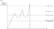
- FIG. 2 illustrates a current level for describing an inverter control for an over-current protection.
- An over-current protection level of the a general-purpose inverter includes a software over-current suppression (S/W OCS) level, a hardware over-current suppression (H/W OCS) level that temporarily blocks PWM of the inverter 100, and an over-current (OC) trip level that stops a driving of the inverter, and the levels are compared with each other as illustrated in FIG. 2 .
- a method for protecting an over-current of the general-purpose inverter includes a slip frequency attenuation of the motor, a temporary output block of the inverter (H/W OCS operation), and a trip stop of the inverter.
- the S/W OSC operation refers to reduce the slip frequency of the motor by attenuating an output frequency of the inverter when the controller of the inverter monitors an output current of the inverter and the output current of the inverter is increased to the S/W OCS level or more.
- the S/W OCS level is generally a fixed level of a rated current or more of the inverter.
- the H/W OCS operation refers to attenuate the output current of the inverter by temporarily blocking an output of the inverter by the controller when an input current is higher than the H/W OCS level.
- the controller of the inverter receives a peak of the maximum value of a three-phase output current of the inverter 100 and senses a hardware signal generated at a predetermined current level or more, and the H/W OCS level is generally higher than the S/W OCS level.
- the controller when the output current of the inverter is an OC trip level or more, the controller generates a trip signal and stops a driving of the inverter.
- the OC trip level is higher than the H/W OCS level, and stops the inverter to protect the inverter and the motor when a sharp current increase such as a short-circuit of the output of the inverter occurs.
- the conventional S/W OCS level is fixed above the rated current of the inverter.
- the S/W OCS operation is performed after the controller of the inverter senses the over-current through a current detection, and is thus delayed according to a filter constant and a current calculation time of the a current detection circuit. Therefore, when the over-current is generated before it is detected that the output current of the inverter arrives at the S/W OCS level due to rapid acceleration of the inverter, the output current of the inverter is increased up to the H/W OCS level or the OC trip level, and thermal stress occurs in the inverter and the motor due to the over-current.
- the S/W OCS level when the S/W OCS level is low, the over-current generated by the increase of the slip frequency of the motor is detected before the H/W OCS level, thereby making it possible to suppress the over-current through the attenuation of the output frequency of the inverter. In this case, however, a continuous overload operation may be limited by the S/W OCS level. In addition, when the S/W OCS level is high, the continuous overload operation of the inverter may be increased, but since a S/W OCS detection time is limited, the current may be increased up to the H/W OCS level or the OC trip level when the slip frequency is rapidly changed by the rapid acceleration of the inverter.
- FIG. 3 is a waveform view for illustrating unbalance of an output current in a single-phase input type inverter.
- the H/W operation is based on the peak of the maximum value of the three-phase output current of the inverter, a margin between the H/W OCS level and the S/W OCS level is decreased when the unbalance 3A of the three-phase output current occurs and the H/W OCS operation occurs more frequently than the three-phase input type inverter having a relatively small unbalance of the three-phase output current. Since the H/W OCS operation is a method that temporarily blocks the output of the inverter, the slip frequency of the motor may be highly increased when large backward torque is applied during a blocking time, and the motor 200 may be stopped when a continuous H/W OCS operation occurs.
- a method for controlling an inverter may include calculating a maximum current from an output current of each phase of the inverter; determining a variable level upper limit by performing a DQ conversion for the output current of each phase of the inverter and adding a change allowable value to the DQ converted output current; determining a difference between the maximum current for each phase and the variable level upper limit as an output frequency attenuation variation, when the output current of the inverter arrives at the variable level upper limit; and determining an output frequency based on the output frequency attenuation variation.
- a variable level lower limit may be further determined by subtracting a variable level band from the variable level upper limit.
- the method may further include maintaining the output frequency when the output current of the inverter is increased from the variable level lower limit to the variable level upper limit.
- the method may further include increasing the output frequency according to a setting to be increased up to a target frequency level when the output current of the inverter is reduced to the variable level lower limit or less.
- the method may further include maintaining the output frequency at a target frequency level, when the output current of the inverter maintains the variable level lower limit.
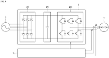
- FIG. 4 is a configuration view schematically illustrating an inverter system to which a control apparatus according to an exemplary embodiment of the present disclosure is applied.
- three-phase power 3 is applied to an inverter 2 and an output of the inverter 2 is applied to a motor 4, and when a three-phase output current of the inverter 2 is applied to a control apparatus 1, a PWM control signal may be output to an inverter unit 2C of the inverter 2.
- the inverter 2 receives AC power from the three phase power, a rectifying unit 2A converts such an AC voltage into a DC voltage, a DC link capacitor 2B stores the DC voltage as a DC link voltage, and the inverter unit 2C then converts the DC link voltage into the AC voltage to output the AC voltage to the motor 4.
- the PWM signal which is output from the control apparatus 1 may control a switching on/off of a plurality of switching elements of the inverter unit 2C to output the AC voltage having a predetermined output frequency to the motor 4.
- FIG. 5 is an illustrative view illustrating a control apparatus of the inverter according to an exemplary embodiment of the present disclosure.
- the control apparatus may include a maximum current calculating unit 10, a level comparing unit 20, a proportional-integral (PI) controller 30, an output frequency attenuation variation calculating unit 40, a converting unit 50, and a level determining unit 60.
- PI proportional-integral
- the maximum current calculating unit 10 may calculate a maximum current from an output current for each phase which is output from the inverter 2. Meanwhile, the converting unit 50 may convert the output current for each phase which is output from the inverter 2 into a DQ coordinate axis. The present disclosure is not limited thereto, however, the converting unit 50 may convert the three-phase output current into a two-phase output current (e.g., a ⁇ ⁇ coordinate axis). However, an example, in which the converting unit 50 converts the output current for each phase into the DQ coordinate axis will be described below.
- the level determining unit 60 may determine a software over-current suppression (S/W OCS) operation level from the DQ converted output current, which is an average of three phases.
- S/W OCS software over-current suppression
- FIG. 6 is a concept view illustrating that the level determining unit of FIG. 5 determines the software over-current suppression (S/W OCS) operation level.
- S/W OCS software over-current suppression
- an S/W OCS maximum current allowable value and an S/W OCS variable level band may be set in advance and stored in a determining unit 70.
- the determining unit 70 may determine S/W OCS variable level high by receiving the DQ converted output current of the inverter 2 and adding the S/W OCS maximum current change allowable value to the DQ converted output current, and may determine an S/W OCS variable level low by receiving the DQ converted output current of the inverter 2 and subtracting the S/W OCS variable level band from the DQ converted output current.
- a level determining unit 60 may be performed, for example, in a time interruption.
- the level comparing unit 30 may determine a difference between the maximum current for each phase and the S/W OCS level.
- the PI controller 40 is to reduce error of an output of the level comparing unit 30, and is a combination of a proportional operation that flexibly approaches a target value and an integral operation in which fine error is accumulated and a control then starts when a predetermined value is exceeded. Since a general operation of the PI controller 40 is widely known, a detailed description thereof will be omitted.
- the output frequency attenuation variation calculating unit 50 may determine the difference between the maximum current for each phase and the S/W OCS level as an output frequency attenuation variation, and a PWM output unit 80 may generate a PWM control signal according to an output frequency and output the PWM control signal to the inverter unit 2C.
- the plurality of switching elements of the inverter unit 2C may output the AC voltage which is switched on or off by the PWM control signal to have a changed output frequency to the motor 4.
- FIG. 7 is an illustrative view illustrating an operation of controlling a software over-current suppression operation according to an exemplary embodiment of the present disclosure.
- the control apparatus 1 may suppress an unnecessary output over-current of the inverter by variably operating the S/W OCS level according to the output current of the inverter.
- the S/W OCS operation level by the variable over-current suppression may be varied according to a level of the output current of the inverter, and when the output current is increased within a normal operation level, the S/W OCS operation level may be operated in proportion to the normal operation level.
- the S/W OCS operation level by the variable over-current suppression may be set in consideration of a filter constant of a current detecting circuit of the inverter, and a delay factor according to a current calculating time 7A.
- FIG. 8 is an illustrative view illustrating a method for adjusting an output frequency of an inverter according to an exemplary embodiment of the present disclosure.
- the S/W OCS operation level for variable over-current suppression may include an S/W OCS variable level upper limit (HIGH) and an S/W OCS variable level lower limit (LOW), and the control apparatus 1 according to an exemplary embodiment of the present disclosure may adjust the output frequency of the inverter 2 according to a state of the output current.
- HGH S/W OCS variable level upper limit
- LOW S/W OCS variable level lower limit
- control apparatus 1 may fix the output frequency of the inverter to suppress an additional increase of the slip frequency of the motor 4 and to suppress the output current of the inverter 2.
- the output current of the inverter 2 may be attenuated by attenuating the output frequency of the inverter 2 to reduce the slip frequency of the motor 4.
- an S/W OCS HIGH flag for determining the attenuation of the output frequency of the inverter 2 may be set, and the output frequency of the inverter 2 may be attenuated until the output current of the inverter 2 drops to the S/W OCS variable level lower limit (LOW) or less. If the output current of the inverter 2 is the S/W OCS variable level or less, the S/W OCS HIGH flag may be reset.
- the output frequency of the inverter 2 may be increased according to a set acceleration time to be increased up to a target frequency level 8E.
- the output frequency of the inverter may be maintained at the target frequency level 8E.
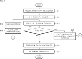
- FIG. 9 is a flow chart illustrating a method for controlling an inverter according to an exemplary embodiment of the present disclosure, and illustrates that the control apparatus 1 controls the S/W OCS operation.
- the inverter 2 is operated by the PWM output provided to the inverter 2 (S11), and as a result, when the output current of the inverter 2 is detected (S12), the maximum current calculating unit 10 may calculate the maximum current from the output current of each phase (S13). Whether or not the S/W OCS is operated is determined by the maximum current of the output current of each phase, and in a case in which the maximum current of the inverter 2 arrives the S/W OCS variable level upper limit (HIGH), the flag may be set to 1 (S16), and the output frequency attenuation variation may be calculated (S17).
- the S/W OCS variable level upper limit
- the converting unit 50 performs the DQ conversion for the output current (S14).
- the level determining unit 70 may determine the S/W OCS variable level upper limit (HIGH) and the S/W OCS variable level lower limit (LOW) (S15) by adding the S/W OCS maximum current change allowable value to and subtracting the S/W OCS variable level band from the DQ converted output current.
- HGH S/W OCS variable level upper limit
- LOW S/W OCS variable level lower limit
- the S/W OCS variable level band determined as described above may be used for the determination of the output frequency attenuation variation (S17). That is, the output frequency attenuation variation calculating unit 40 may determine a difference between the maximum current for each phase and the S/W OCS variable level upper limit (HIGH) as the output frequency attenuation variation.
- HIGH S/W OCS variable level upper limit
- the output frequency may be calculated based on the attenuation variation determined as described above (S18).
- the output frequency may be calculated without changing the output frequency (S18). That is, in the section 8A of FIG. 8 , the output frequency may be output while maintaining the output frequency.
- the PWM output unit 70 may output the PWM signal for outputting to the inverter unit 2C of the inverter 2 using the output frequency determined as described above (S19).
- the unnecessary increase of the output current of the inverter may be suppressed in the rapid acceleration operation in which the slip frequency of the motor is rapidly changed.
- the inverter may be stably accelerated, and the control performance of the motor may be stably secured by continuously controlling the inverter by the S/W OCS operation by the variable over-current suppression.
Abstract
Description
- The present disclosure relates to a method for controlling an inverter.
- Typically, an inverter receives AC mains electricity to converter it into a DC power, and then converts it again into an AC power suitable for electric motors to supply it. Such an inverter effectively controls an electric motor, thereby reducing the power consumption of the motor to improve energy efficiency.
-
FIG. 1 is a schematic configuration view of a general inverter. - An
inverter 100 receives an AC power of three phases, the rectifyingunit 110 converts such an AC voltage into a DC voltage, aDC link capacitor 120 stores the DC voltage as a DC link voltage, and aninverter unit 130 then converts the DC link voltage into the AC voltage to drive amotor 200. Theinverter 100 is typically controlled by a variable voltage variable frequency (VVVF) manner, and theinverter unit 130 varies magnitude and frequency of a voltage which is input to themotor 200 according to a pulse width modulation (PWM) output to control a speed of themotor 200. - A slip frequency of the
motor 200 is defined as a difference between a command frequency generated by theinverter 100 and a speed of revolution of themotor 200, and when the slip frequency of themotor 200 is greatly increased, an over-current is generated and theinverter 100 or themotor 200 is damaged. Since theinverter 100 has a protection solution for the over-current, a controller suppresses the over-current or generates a trip when the over-current is generated, thereby protecting theinverter 100 or themotor 200. -
FIG. 2 illustrates a current level for describing an inverter control for an over-current protection. - An over-current protection level of the a general-purpose inverter includes a software over-current suppression (S/W OCS) level, a hardware over-current suppression (H/W OCS) level that temporarily blocks PWM of the
inverter 100, and an over-current (OC) trip level that stops a driving of the inverter, and the levels are compared with each other as illustrated inFIG. 2 . A method for protecting an over-current of the general-purpose inverter includes a slip frequency attenuation of the motor, a temporary output block of the inverter (H/W OCS operation), and a trip stop of the inverter. - Among them, the S/W OSC operation refers to reduce the slip frequency of the motor by attenuating an output frequency of the inverter when the controller of the inverter monitors an output current of the inverter and the output current of the inverter is increased to the S/W OCS level or more. The S/W OCS level is generally a fixed level of a rated current or more of the inverter.
- In addition, the H/W OCS operation refers to attenuate the output current of the inverter by temporarily blocking an output of the inverter by the controller when an input current is higher than the H/W OCS level. The controller of the inverter receives a peak of the maximum value of a three-phase output current of the
inverter 100 and senses a hardware signal generated at a predetermined current level or more, and the H/W OCS level is generally higher than the S/W OCS level. - Finally, according to the trip stop method of the inverter, when the output current of the inverter is an OC trip level or more, the controller generates a trip signal and stops a driving of the inverter. The OC trip level is higher than the H/W OCS level, and stops the inverter to protect the inverter and the motor when a sharp current increase such as a short-circuit of the output of the inverter occurs.
- In the control methods as described above, the conventional S/W OCS level is fixed above the rated current of the inverter. The S/W OCS operation is performed after the controller of the inverter senses the over-current through a current detection, and is thus delayed according to a filter constant and a current calculation time of the a current detection circuit. Therefore, when the over-current is generated before it is detected that the output current of the inverter arrives at the S/W OCS level due to rapid acceleration of the inverter, the output current of the inverter is increased up to the H/W OCS level or the OC trip level, and thermal stress occurs in the inverter and the motor due to the over-current.
- In addition, when the S/W OCS level is low, the over-current generated by the increase of the slip frequency of the motor is detected before the H/W OCS level, thereby making it possible to suppress the over-current through the attenuation of the output frequency of the inverter. In this case, however, a continuous overload operation may be limited by the S/W OCS level. In addition, when the S/W OCS level is high, the continuous overload operation of the inverter may be increased, but since a S/W OCS detection time is limited, the current may be increased up to the H/W OCS level or the OC trip level when the slip frequency is rapidly changed by the rapid acceleration of the inverter.
- Meanwhile, a three-phase output current of a single-phase input type inverter causes unbalance due to a DC link voltage ripple.
FIG. 3 is a waveform view for illustrating unbalance of an output current in a single-phase input type inverter. - Since the H/W operation is based on the peak of the maximum value of the three-phase output current of the inverter, a margin between the H/W OCS level and the S/W OCS level is decreased when the
unbalance 3A of the three-phase output current occurs and the H/W OCS operation occurs more frequently than the three-phase input type inverter having a relatively small unbalance of the three-phase output current. Since the H/W OCS operation is a method that temporarily blocks the output of the inverter, the slip frequency of the motor may be highly increased when large backward torque is applied during a blocking time, and themotor 200 may be stopped when a continuous H/W OCS operation occurs. - It is an object of the present disclosure to provide a method for controlling an inverter in which a software over-current suppression operation level is varied according to an output current level of the inverter.
- Objects of the present disclosure are not limited to the above-described objects and other objects and advantages can be appreciated by those skilled in the art from the following descriptions. Further, it will be easily appreciated that the objects and advantages of the present disclosure can be practiced by means recited in the appended claims and a combination thereof.
- In accordance with one aspect of the present disclosure, a method for controlling an inverter may include calculating a maximum current from an output current of each phase of the inverter; determining a variable level upper limit by performing a DQ conversion for the output current of each phase of the inverter and adding a change allowable value to the DQ converted output current; determining a difference between the maximum current for each phase and the variable level upper limit as an output frequency attenuation variation, when the output current of the inverter arrives at the variable level upper limit; and determining an output frequency based on the output frequency attenuation variation.
- In the determining of the variable level upper limit, a variable level lower limit may be further determined by subtracting a variable level band from the variable level upper limit.
- The method may further include maintaining the output frequency when the output current of the inverter is increased from the variable level lower limit to the variable level upper limit.
- The method may further include increasing the output frequency according to a setting to be increased up to a target frequency level when the output current of the inverter is reduced to the variable level lower limit or less.
- The method may further include maintaining the output frequency at a target frequency level, when the output current of the inverter maintains the variable level lower limit.
-
-
FIG. 1 is a schematic configuration view of a general inverter; -
FIG. 2 illustrates a current level for describing an inverter control for an over-current protection; -
FIG. 3 is a waveform view for illustrating unbalance of an output current in a single-phase input type inverter; -
FIG. 4 is a configuration view schematically illustrating an inverter system to which a control apparatus according to an exemplary embodiment of the present disclosure is applied; -
FIG. 5 is an illustrative view illustrating a control apparatus of the inverter according to an exemplary embodiment of the present disclosure; -
FIG. 6 is a concept view illustrating that a level determining unit ofFIG. 5 determines a software over-current suppression operation level; -
FIG. 7 is an illustrative view illustrating an operation of controlling a software over-current suppression operation according to an exemplary embodiment of the present disclosure; -
FIG. 8 is an illustrative view illustrating a method for adjusting an output frequency of an inverter according to an exemplary embodiment of the present disclosure; and -
FIG. 9 is a flow chart illustrating a method for controlling an inverter according to an exemplary embodiment of the present disclosure. - Exemplary embodiments of the present disclosure will now be described in detail with reference to the accompanying drawings to facilitate understanding of the configuration and effects thereof. The scope of the present disclosure may, however, be embodied in many different forms and should not be construed as limited to the embodiments set forth herein. These embodiments are provided so that this disclosure will be thorough and complete, and will fully convey the scope of the inventive subject matter to those skilled in the art. In the drawings, the size of some of the elements may be exaggerated for convenience of illustration and not drawn on scale for illustrative purposes.
- It will be understood that when an element such as a layer, region, substrate, or panel is referred to as being "on" or "connected to" another element, it can be directly on the other element or intervening elements may also be present. In contrast, when an element is referred to as being "directly on" or "directly connected to" another element, there are no intervening elements present. The same may be applied to other expressions for describing relationship between elements such as "between" and "directly between".
- Terms such as first, second, etc. in the description and in the claims are used for distinguishing between similar elements and not necessarily for describing a sequential or chronological order. The terms are only used to differentiate one component from other components. For example, the terms so used are interchangeable under appropriate circumstances without departing from the scope of the present disclosure.
- As used herein, the singular form of "a", "an", and "the" includes plural references unless the context clearly dictates otherwise. It will be further understood that the terms "comprises" or "have" used in this specification, specify the presence of stated features, steps, operations, components, parts, or a combination thereof, but do not preclude the presence or addition of one or more other features, numerals, steps, operations, components, parts, or a combination thereof.
- The terms used herein, including technical terms, have the same meanings as terms that are generally understood by those skilled in the art, as long as the terms are not explicitly defined differently.
- Hereinafter, exemplary embodiments of the present disclosure will be described in detail with reference to the accompanying drawings.
-
FIG. 4 is a configuration view schematically illustrating an inverter system to which a control apparatus according to an exemplary embodiment of the present disclosure is applied. - As illustrated in
FIG. 4 , in a system to which an exemplary embodiment of the present disclosure is applied, three-phase power 3 is applied to aninverter 2 and an output of theinverter 2 is applied to a motor 4, and when a three-phase output current of theinverter 2 is applied to acontrol apparatus 1, a PWM control signal may be output to an inverter unit 2C of theinverter 2. - The
inverter 2 receives AC power from the three phase power, arectifying unit 2A converts such an AC voltage into a DC voltage, aDC link capacitor 2B stores the DC voltage as a DC link voltage, and the inverter unit 2C then converts the DC link voltage into the AC voltage to output the AC voltage to the motor 4. - The PWM signal which is output from the
control apparatus 1 may control a switching on/off of a plurality of switching elements of the inverter unit 2C to output the AC voltage having a predetermined output frequency to the motor 4. -
FIG. 5 is an illustrative view illustrating a control apparatus of the inverter according to an exemplary embodiment of the present disclosure. - As illustrated in
FIG. 5 , the control apparatus according to an exemplary embodiment of the present disclosure may include a maximum current calculatingunit 10, alevel comparing unit 20, a proportional-integral (PI)controller 30, an output frequency attenuationvariation calculating unit 40, a convertingunit 50, and alevel determining unit 60. - The maximum current calculating
unit 10 may calculate a maximum current from an output current for each phase which is output from theinverter 2. Meanwhile, the convertingunit 50 may convert the output current for each phase which is output from theinverter 2 into a DQ coordinate axis. The present disclosure is not limited thereto, however, the convertingunit 50 may convert the three-phase output current into a two-phase output current (e.g., a α β coordinate axis). However, an example, in which the convertingunit 50 converts the output current for each phase into the DQ coordinate axis will be described below. - The
level determining unit 60 may determine a software over-current suppression (S/W OCS) operation level from the DQ converted output current, which is an average of three phases. -
FIG. 6 is a concept view illustrating that the level determining unit ofFIG. 5 determines the software over-current suppression (S/W OCS) operation level. - As illustrated in
FIG. 6 , an S/W OCS maximum current allowable value and an S/W OCS variable level band may be set in advance and stored in a determiningunit 70. The determiningunit 70 may determine S/W OCS variable level high by receiving the DQ converted output current of theinverter 2 and adding the S/W OCS maximum current change allowable value to the DQ converted output current, and may determine an S/W OCS variable level low by receiving the DQ converted output current of theinverter 2 and subtracting the S/W OCS variable level band from the DQ converted output current. Such alevel determining unit 60 may be performed, for example, in a time interruption. - Referring again to
FIG. 5 , thelevel comparing unit 30 may determine a difference between the maximum current for each phase and the S/W OCS level. ThePI controller 40 is to reduce error of an output of thelevel comparing unit 30, and is a combination of a proportional operation that flexibly approaches a target value and an integral operation in which fine error is accumulated and a control then starts when a predetermined value is exceeded. Since a general operation of thePI controller 40 is widely known, a detailed description thereof will be omitted. - As such, the output frequency attenuation
variation calculating unit 50 may determine the difference between the maximum current for each phase and the S/W OCS level as an output frequency attenuation variation, and a PWM output unit 80 may generate a PWM control signal according to an output frequency and output the PWM control signal to the inverter unit 2C. The plurality of switching elements of the inverter unit 2C may output the AC voltage which is switched on or off by the PWM control signal to have a changed output frequency to the motor 4. -
FIG. 7 is an illustrative view illustrating an operation of controlling a software over-current suppression operation according to an exemplary embodiment of the present disclosure. - The
control apparatus 1 according to an exemplary embodiment of the present disclosure may suppress an unnecessary output over-current of the inverter by variably operating the S/W OCS level according to the output current of the inverter. The S/W OCS operation level by the variable over-current suppression may be varied according to a level of the output current of the inverter, and when the output current is increased within a normal operation level, the S/W OCS operation level may be operated in proportion to the normal operation level. The S/W OCS operation level by the variable over-current suppression may be set in consideration of a filter constant of a current detecting circuit of the inverter, and a delay factor according to acurrent calculating time 7A. -
FIG. 8 is an illustrative view illustrating a method for adjusting an output frequency of an inverter according to an exemplary embodiment of the present disclosure. - As illustrated in
FIG. 8 , the S/W OCS operation level for variable over-current suppression may include an S/W OCS variable level upper limit (HIGH) and an S/W OCS variable level lower limit (LOW), and thecontrol apparatus 1 according to an exemplary embodiment of the present disclosure may adjust the output frequency of theinverter 2 according to a state of the output current. - In a
section 8A in which the output current of theinverter 2 enters the S/W OCS variable level lower limit (LOW), thecontrol apparatus 1 may fix the output frequency of the inverter to suppress an additional increase of the slip frequency of the motor 4 and to suppress the output current of theinverter 2. - In a
section 8B in which the output current of theinverter 2 enters the S/W OCS variable level upper limit (HIGH), the output current of theinverter 2 may be attenuated by attenuating the output frequency of theinverter 2 to reduce the slip frequency of the motor 4. In this case, an S/W OCS HIGH flag for determining the attenuation of the output frequency of theinverter 2 may be set, and the output frequency of theinverter 2 may be attenuated until the output current of theinverter 2 drops to the S/W OCS variable level lower limit (LOW) or less. If the output current of theinverter 2 is the S/W OCS variable level or less, the S/W OCS HIGH flag may be reset. - In a
section 8C in which the output current of theinverter 2 is reduced from the S/W OCS variable level upper limit (HIGH) to the S/W OCS variable level lower limit (LOW) or less, the output frequency of theinverter 2 may be increased according to a set acceleration time to be increased up to atarget frequency level 8E. - In a second 8D in which the output current of the
inverter 2 enters the S/W OCS variable level lower limit (LOW), the output frequency of the inverter may be maintained at thetarget frequency level 8E. -
FIG. 9 is a flow chart illustrating a method for controlling an inverter according to an exemplary embodiment of the present disclosure, and illustrates that thecontrol apparatus 1 controls the S/W OCS operation. - As illustrated in
FIG. 9 , in the method for controlling the inverter according to an exemplary embodiment of the present disclosure, theinverter 2 is operated by the PWM output provided to the inverter 2 (S11), and as a result, when the output current of theinverter 2 is detected (S12), the maximum current calculatingunit 10 may calculate the maximum current from the output current of each phase (S13). Whether or not the S/W OCS is operated is determined by the maximum current of the output current of each phase, and in a case in which the maximum current of theinverter 2 arrives the S/W OCS variable level upper limit (HIGH), the flag may be set to 1 (S16), and the output frequency attenuation variation may be calculated (S17). - In this case, the converting
unit 50 performs the DQ conversion for the output current (S14). - Next, the
level determining unit 70 may determine the S/W OCS variable level upper limit (HIGH) and the S/W OCS variable level lower limit (LOW) (S15) by adding the S/W OCS maximum current change allowable value to and subtracting the S/W OCS variable level band from the DQ converted output current. - Next, the S/W OCS variable level band determined as described above may be used for the determination of the output frequency attenuation variation (S17). That is, the output frequency attenuation
variation calculating unit 40 may determine a difference between the maximum current for each phase and the S/W OCS variable level upper limit (HIGH) as the output frequency attenuation variation. - The output frequency may be calculated based on the attenuation variation determined as described above (S18).
- In addition, in a case in which the maximum current of the
inverter 2 is not the S/W OCS variable level upper limit (HIGH) in S16, the output frequency may be calculated without changing the output frequency (S18). That is, in thesection 8A ofFIG. 8 , the output frequency may be output while maintaining the output frequency. - The
PWM output unit 70 may output the PWM signal for outputting to the inverter unit 2C of theinverter 2 using the output frequency determined as described above (S19). - According to the exemplary embodiments of the present disclosure, when the S/W OCS by the variable over-current suppression is applied, the unnecessary increase of the output current of the inverter may be suppressed in the rapid acceleration operation in which the slip frequency of the motor is rapidly changed.
- In addition, even in a situation in which the large inertia load in which the slip frequency of the motor according to the acceleration time is increased is applied, the inverter may be stably accelerated, and the control performance of the motor may be stably secured by continuously controlling the inverter by the S/W OCS operation by the variable over-current suppression.
- As described above, according to the exemplary embodiments of the present disclosure, when the S/W OCS by the variable over-current suppression is applied, the unnecessary increase of the output current of the inverter may be suppressed in the rapid acceleration operation in which the slip frequency of the motor is rapidly changed.
- In addition, according to the present disclosure, even in a situation in which the large inertia load in which the slip frequency of the motor according to the acceleration time is increased is applied, the inverter may be stably accelerated, and the control performance of the motor may be stably secured by continuously controlling the inverter by the S/W OCS operation by the variable over-current suppression.
- Although the exemplary embodiments of the present disclosure have been described in detail, these are merely illustrative. It will be appreciated by those skilled in the art that various modifications and equivalents are possible without departing from the scope of the present disclosure. Accordingly, the true scope of the present disclosure sought to be protected is defined only by the appended claims.
Claims (5)
- A method for controlling an inverter (2) of a control apparatus (1) controlling the inverter (2), the method comprising:calculating a maximum current from an output current of each phase of the inverter (2);determining a variable level upper limit by performing a DQ conversion for the output current of each phase of the inverter (2) and adding a change allowable value to the DQ converted output current;determining a difference between the maximum current for each phase and the variable level upper limit as an output frequency attenuation variation, when the output current of the inverter (2) arrives at the variable level upper limit; anddetermining an output frequency based on the output frequency attenuation variation.
- The method of claim 1, wherein the determining of the variable level upper limit further comprises determining a variable level lower limit by subtracting a variable level band from the variable level upper limit.
- The method of claim 2, further comprising:maintaining the output frequency when the output current of the inverter (2) is increased from the variable level lower limit to the variable level upper limit.
- The method of claim 2, further comprising:increasing the output frequency according to a setting to be increased up to a target frequency level when the output current of the inverter (2) is reduced to the variable level lower limit or less.
- The method of claim 2, further comprising:maintaining the output frequency at a target frequency level, when the output current of the inverter (2) maintains the variable level lower limit.
Applications Claiming Priority (1)
| Application Number | Priority Date | Filing Date | Title |
|---|---|---|---|
| KR1020160179241A KR102485408B1 (en) | 2016-12-26 | 2016-12-26 | Method for controlling inverter |
Publications (2)
| Publication Number | Publication Date |
|---|---|
| EP3340459A1 true EP3340459A1 (en) | 2018-06-27 |
| EP3340459B1 EP3340459B1 (en) | 2021-06-02 |
Family
ID=60673330
Family Applications (1)
| Application Number | Title | Priority Date | Filing Date |
|---|---|---|---|
| EP17206905.6A Active EP3340459B1 (en) | 2016-12-26 | 2017-12-13 | Method for controlling inverter |
Country Status (6)
| Country | Link |
|---|---|
| US (1) | US10014764B1 (en) |
| EP (1) | EP3340459B1 (en) |
| JP (1) | JP6448757B2 (en) |
| KR (1) | KR102485408B1 (en) |
| CN (1) | CN108242899B (en) |
| ES (1) | ES2883136T3 (en) |
Families Citing this family (2)
| Publication number | Priority date | Publication date | Assignee | Title |
|---|---|---|---|---|
| KR102645551B1 (en) * | 2017-02-23 | 2024-03-07 | 엘에스일렉트릭(주) | Apparatus for controlling inverter in forming machine system |
| KR102186763B1 (en) | 2019-04-11 | 2020-12-04 | 엘에스일렉트릭(주) | Overcurrent protection inverter |
Citations (4)
| Publication number | Priority date | Publication date | Assignee | Title |
|---|---|---|---|---|
| US5247237A (en) * | 1991-09-06 | 1993-09-21 | Mitsubishi Denki Kabushiki Kaisha | Control device of induction motor |
| JPH0767311B2 (en) * | 1987-07-16 | 1995-07-19 | 富士電機株式会社 | Current and torque limiting circuit for AC motor drive inverter device |
| EP2043252A1 (en) * | 2007-09-26 | 2009-04-01 | Jtekt Corporation | Motor controller and electric power steering apparatus |
| WO2016121113A1 (en) * | 2015-01-30 | 2016-08-04 | 三菱電機株式会社 | Inverter device |
Family Cites Families (14)
| Publication number | Priority date | Publication date | Assignee | Title |
|---|---|---|---|---|
| JPH06284787A (en) | 1993-03-30 | 1994-10-07 | Toshiba Corp | Method for preventing overcurrent stall of inverter device and inverter device |
| JP3299417B2 (en) * | 1995-07-28 | 2002-07-08 | 松下電工株式会社 | Inverter device |
| JPH09182493A (en) * | 1995-12-27 | 1997-07-11 | Matsushita Electric Ind Co Ltd | Inverter control method for air conditioner and its controller |
| WO1997050162A1 (en) | 1996-06-26 | 1997-12-31 | Hitachi, Ltd. | Motor driving apparatus |
| JP2000201484A (en) | 1998-12-29 | 2000-07-18 | Omron Corp | Inverter equipment |
| JP4051601B2 (en) * | 2001-12-17 | 2008-02-27 | 富士電機機器制御株式会社 | Variable speed control device for electric motor |
| EP2320549B1 (en) * | 2009-11-05 | 2014-03-12 | Siemens Aktiengesellschaft | Method of operating an inverter and inverter control arrangement |
| WO2012086674A1 (en) * | 2010-12-22 | 2012-06-28 | 富士電機株式会社 | Power conversion apparatus |
| JP5485232B2 (en) * | 2011-07-04 | 2014-05-07 | 本田技研工業株式会社 | Switching circuit control device |
| US9160271B2 (en) * | 2012-01-18 | 2015-10-13 | Mitsubishi Electric Corporation | Power conversion device |
| KR101552771B1 (en) | 2013-12-06 | 2015-09-11 | 엘에스산전 주식회사 | Method for limiting over-current in inverter |
| JP6709014B2 (en) * | 2014-04-18 | 2020-06-10 | 日立オートモティブシステムズ株式会社 | Inverter device |
| JP6465477B2 (en) * | 2014-11-20 | 2019-02-06 | 三菱重工業株式会社 | Motor control device, motor control method and program |
| JP7067311B2 (en) * | 2018-06-26 | 2022-05-16 | 株式会社デンソー | Control method of vehicle cleaning device, vehicle cleaning system and vehicle cleaning system |
-
2016
- 2016-12-26 KR KR1020160179241A patent/KR102485408B1/en active IP Right Grant
-
2017
- 2017-12-13 EP EP17206905.6A patent/EP3340459B1/en active Active
- 2017-12-13 ES ES17206905T patent/ES2883136T3/en active Active
- 2017-12-19 JP JP2017243197A patent/JP6448757B2/en not_active Expired - Fee Related
- 2017-12-19 US US15/847,299 patent/US10014764B1/en active Active
- 2017-12-25 CN CN201711423919.1A patent/CN108242899B/en active Active
Patent Citations (4)
| Publication number | Priority date | Publication date | Assignee | Title |
|---|---|---|---|---|
| JPH0767311B2 (en) * | 1987-07-16 | 1995-07-19 | 富士電機株式会社 | Current and torque limiting circuit for AC motor drive inverter device |
| US5247237A (en) * | 1991-09-06 | 1993-09-21 | Mitsubishi Denki Kabushiki Kaisha | Control device of induction motor |
| EP2043252A1 (en) * | 2007-09-26 | 2009-04-01 | Jtekt Corporation | Motor controller and electric power steering apparatus |
| WO2016121113A1 (en) * | 2015-01-30 | 2016-08-04 | 三菱電機株式会社 | Inverter device |
Also Published As
| Publication number | Publication date |
|---|---|
| JP6448757B2 (en) | 2019-01-09 |
| CN108242899A (en) | 2018-07-03 |
| US10014764B1 (en) | 2018-07-03 |
| EP3340459B1 (en) | 2021-06-02 |
| JP2018108019A (en) | 2018-07-05 |
| US20180183322A1 (en) | 2018-06-28 |
| KR20180075187A (en) | 2018-07-04 |
| CN108242899B (en) | 2020-12-22 |
| KR102485408B1 (en) | 2023-01-04 |
| ES2883136T3 (en) | 2021-12-07 |
Similar Documents
| Publication | Publication Date | Title |
|---|---|---|
| CN108292902B (en) | Hybrid drive circuit and control method for variable speed induction motor system | |
| US8264209B2 (en) | Method of and apparatus for operating a double-fed asynchronous machine in the event of transient mains voltage changes | |
| EP2096747B1 (en) | Motor driving apparatus | |
| US5969498A (en) | Induction motor controller | |
| CN107836077B (en) | Motor control device | |
| JP4461877B2 (en) | Inverter device | |
| US5747833A (en) | Apparatus for driving induction motor | |
| US9762138B2 (en) | Power conversion device | |
| US10014764B1 (en) | Method for controlling inverter | |
| US7091690B1 (en) | Power conversion device | |
| US10256753B2 (en) | AC motor systems with drive circuits and methods of use | |
| JP6258806B2 (en) | Power converter for grid connection | |
| KR102416374B1 (en) | Apparatus for controlling dc link voltage in power cell of medium voltage inverter | |
| CN108631692B (en) | Method for controlling an inverter | |
| CN112583243B (en) | Hardware current limiting method and device for frequency converter and storage medium | |
| JP3490600B2 (en) | Pulse width modulation method for power converter | |
| JP3462347B2 (en) | Control device for variable speed generator motor | |
| EP3229364B1 (en) | Inverter | |
| JP2009153248A (en) | Pwm cyclone converter and control method of the same | |
| JP2002272181A (en) | Power conversion apparatus | |
| JP4017933B2 (en) | AC excitation type generator motor | |
| KR100283912B1 (en) | Reduction Device of Induction Motor | |
| CN116365587A (en) | Method for inhibiting magnetic saturation of transformer and power conversion device | |
| JPH0440957B2 (en) |
Legal Events
| Date | Code | Title | Description |
|---|---|---|---|
| PUAI | Public reference made under article 153(3) epc to a published international application that has entered the european phase |
Free format text: ORIGINAL CODE: 0009012 |
|
| STAA | Information on the status of an ep patent application or granted ep patent |
Free format text: STATUS: THE APPLICATION HAS BEEN PUBLISHED |
|
| AK | Designated contracting states |
Kind code of ref document: A1 Designated state(s): AL AT BE BG CH CY CZ DE DK EE ES FI FR GB GR HR HU IE IS IT LI LT LU LV MC MK MT NL NO PL PT RO RS SE SI SK SM TR |
|
| AX | Request for extension of the european patent |
Extension state: BA ME |
|
| STAA | Information on the status of an ep patent application or granted ep patent |
Free format text: STATUS: REQUEST FOR EXAMINATION WAS MADE |
|
| 17P | Request for examination filed |
Effective date: 20181221 |
|
| RBV | Designated contracting states (corrected) |
Designated state(s): AL AT BE BG CH CY CZ DE DK EE ES FI FR GB GR HR HU IE IS IT LI LT LU LV MC MK MT NL NO PL PT RO RS SE SI SK SM TR |
|
| STAA | Information on the status of an ep patent application or granted ep patent |
Free format text: STATUS: EXAMINATION IS IN PROGRESS |
|
| 17Q | First examination report despatched |
Effective date: 20200818 |
|
| STAA | Information on the status of an ep patent application or granted ep patent |
Free format text: STATUS: EXAMINATION IS IN PROGRESS |
|
| GRAP | Despatch of communication of intention to grant a patent |
Free format text: ORIGINAL CODE: EPIDOSNIGR1 |
|
| STAA | Information on the status of an ep patent application or granted ep patent |
Free format text: STATUS: GRANT OF PATENT IS INTENDED |
|
| RIC1 | Information provided on ipc code assigned before grant |
Ipc: H02P 27/08 20060101ALN20210118BHEP Ipc: H02P 29/028 20160101ALI20210118BHEP Ipc: H02P 29/032 20160101ALI20210118BHEP Ipc: H02P 29/024 20160101AFI20210118BHEP |
|
| INTG | Intention to grant announced |
Effective date: 20210209 |
|
| GRAS | Grant fee paid |
Free format text: ORIGINAL CODE: EPIDOSNIGR3 |
|
| GRAA | (expected) grant |
Free format text: ORIGINAL CODE: 0009210 |
|
| STAA | Information on the status of an ep patent application or granted ep patent |
Free format text: STATUS: THE PATENT HAS BEEN GRANTED |
|
| REG | Reference to a national code |
Ref country code: CH Ref legal event code: EP |
|
| AK | Designated contracting states |
Kind code of ref document: B1 Designated state(s): AL AT BE BG CH CY CZ DE DK EE ES FI FR GB GR HR HU IE IS IT LI LT LU LV MC MK MT NL NO PL PT RO RS SE SI SK SM TR |
|
| REG | Reference to a national code |
Ref country code: GB Ref legal event code: FG4D |
|
| REG | Reference to a national code |
Ref country code: AT Ref legal event code: REF Ref document number: 1399388 Country of ref document: AT Kind code of ref document: T Effective date: 20210615 |
|
| REG | Reference to a national code |
Ref country code: IE Ref legal event code: FG4D |
|
| REG | Reference to a national code |
Ref country code: DE Ref legal event code: R096 Ref document number: 602017039598 Country of ref document: DE |
|
| REG | Reference to a national code |
Ref country code: LT Ref legal event code: MG9D |
|
| PG25 | Lapsed in a contracting state [announced via postgrant information from national office to epo] |
Ref country code: LT Free format text: LAPSE BECAUSE OF FAILURE TO SUBMIT A TRANSLATION OF THE DESCRIPTION OR TO PAY THE FEE WITHIN THE PRESCRIBED TIME-LIMIT Effective date: 20210602 Ref country code: FI Free format text: LAPSE BECAUSE OF FAILURE TO SUBMIT A TRANSLATION OF THE DESCRIPTION OR TO PAY THE FEE WITHIN THE PRESCRIBED TIME-LIMIT Effective date: 20210602 Ref country code: BG Free format text: LAPSE BECAUSE OF FAILURE TO SUBMIT A TRANSLATION OF THE DESCRIPTION OR TO PAY THE FEE WITHIN THE PRESCRIBED TIME-LIMIT Effective date: 20210902 Ref country code: HR Free format text: LAPSE BECAUSE OF FAILURE TO SUBMIT A TRANSLATION OF THE DESCRIPTION OR TO PAY THE FEE WITHIN THE PRESCRIBED TIME-LIMIT Effective date: 20210602 |
|
| REG | Reference to a national code |
Ref country code: NL Ref legal event code: MP Effective date: 20210602 |
|
| REG | Reference to a national code |
Ref country code: AT Ref legal event code: MK05 Ref document number: 1399388 Country of ref document: AT Kind code of ref document: T Effective date: 20210602 |
|
| PG25 | Lapsed in a contracting state [announced via postgrant information from national office to epo] |
Ref country code: GR Free format text: LAPSE BECAUSE OF FAILURE TO SUBMIT A TRANSLATION OF THE DESCRIPTION OR TO PAY THE FEE WITHIN THE PRESCRIBED TIME-LIMIT Effective date: 20210903 Ref country code: LV Free format text: LAPSE BECAUSE OF FAILURE TO SUBMIT A TRANSLATION OF THE DESCRIPTION OR TO PAY THE FEE WITHIN THE PRESCRIBED TIME-LIMIT Effective date: 20210602 Ref country code: NO Free format text: LAPSE BECAUSE OF FAILURE TO SUBMIT A TRANSLATION OF THE DESCRIPTION OR TO PAY THE FEE WITHIN THE PRESCRIBED TIME-LIMIT Effective date: 20210902 Ref country code: PL Free format text: LAPSE BECAUSE OF FAILURE TO SUBMIT A TRANSLATION OF THE DESCRIPTION OR TO PAY THE FEE WITHIN THE PRESCRIBED TIME-LIMIT Effective date: 20210602 Ref country code: RS Free format text: LAPSE BECAUSE OF FAILURE TO SUBMIT A TRANSLATION OF THE DESCRIPTION OR TO PAY THE FEE WITHIN THE PRESCRIBED TIME-LIMIT Effective date: 20210602 Ref country code: SE Free format text: LAPSE BECAUSE OF FAILURE TO SUBMIT A TRANSLATION OF THE DESCRIPTION OR TO PAY THE FEE WITHIN THE PRESCRIBED TIME-LIMIT Effective date: 20210602 |
|
| REG | Reference to a national code |
Ref country code: ES Ref legal event code: FG2A Ref document number: 2883136 Country of ref document: ES Kind code of ref document: T3 Effective date: 20211207 |
|
| PG25 | Lapsed in a contracting state [announced via postgrant information from national office to epo] |
Ref country code: SM Free format text: LAPSE BECAUSE OF FAILURE TO SUBMIT A TRANSLATION OF THE DESCRIPTION OR TO PAY THE FEE WITHIN THE PRESCRIBED TIME-LIMIT Effective date: 20210602 Ref country code: SK Free format text: LAPSE BECAUSE OF FAILURE TO SUBMIT A TRANSLATION OF THE DESCRIPTION OR TO PAY THE FEE WITHIN THE PRESCRIBED TIME-LIMIT Effective date: 20210602 Ref country code: CZ Free format text: LAPSE BECAUSE OF FAILURE TO SUBMIT A TRANSLATION OF THE DESCRIPTION OR TO PAY THE FEE WITHIN THE PRESCRIBED TIME-LIMIT Effective date: 20210602 Ref country code: EE Free format text: LAPSE BECAUSE OF FAILURE TO SUBMIT A TRANSLATION OF THE DESCRIPTION OR TO PAY THE FEE WITHIN THE PRESCRIBED TIME-LIMIT Effective date: 20210602 Ref country code: AT Free format text: LAPSE BECAUSE OF FAILURE TO SUBMIT A TRANSLATION OF THE DESCRIPTION OR TO PAY THE FEE WITHIN THE PRESCRIBED TIME-LIMIT Effective date: 20210602 Ref country code: NL Free format text: LAPSE BECAUSE OF FAILURE TO SUBMIT A TRANSLATION OF THE DESCRIPTION OR TO PAY THE FEE WITHIN THE PRESCRIBED TIME-LIMIT Effective date: 20210602 Ref country code: PT Free format text: LAPSE BECAUSE OF FAILURE TO SUBMIT A TRANSLATION OF THE DESCRIPTION OR TO PAY THE FEE WITHIN THE PRESCRIBED TIME-LIMIT Effective date: 20211004 Ref country code: RO Free format text: LAPSE BECAUSE OF FAILURE TO SUBMIT A TRANSLATION OF THE DESCRIPTION OR TO PAY THE FEE WITHIN THE PRESCRIBED TIME-LIMIT Effective date: 20210602 |
|
| REG | Reference to a national code |
Ref country code: DE Ref legal event code: R097 Ref document number: 602017039598 Country of ref document: DE |
|
| PLBE | No opposition filed within time limit |
Free format text: ORIGINAL CODE: 0009261 |
|
| STAA | Information on the status of an ep patent application or granted ep patent |
Free format text: STATUS: NO OPPOSITION FILED WITHIN TIME LIMIT |
|
| PG25 | Lapsed in a contracting state [announced via postgrant information from national office to epo] |
Ref country code: DK Free format text: LAPSE BECAUSE OF FAILURE TO SUBMIT A TRANSLATION OF THE DESCRIPTION OR TO PAY THE FEE WITHIN THE PRESCRIBED TIME-LIMIT Effective date: 20210602 |
|
| 26N | No opposition filed |
Effective date: 20220303 |
|
| PG25 | Lapsed in a contracting state [announced via postgrant information from national office to epo] |
Ref country code: AL Free format text: LAPSE BECAUSE OF FAILURE TO SUBMIT A TRANSLATION OF THE DESCRIPTION OR TO PAY THE FEE WITHIN THE PRESCRIBED TIME-LIMIT Effective date: 20210602 |
|
| PG25 | Lapsed in a contracting state [announced via postgrant information from national office to epo] |
Ref country code: MC Free format text: LAPSE BECAUSE OF FAILURE TO SUBMIT A TRANSLATION OF THE DESCRIPTION OR TO PAY THE FEE WITHIN THE PRESCRIBED TIME-LIMIT Effective date: 20210602 |
|
| REG | Reference to a national code |
Ref country code: CH Ref legal event code: PL |
|
| REG | Reference to a national code |
Ref country code: BE Ref legal event code: MM Effective date: 20211231 |
|
| PG25 | Lapsed in a contracting state [announced via postgrant information from national office to epo] |
Ref country code: LU Free format text: LAPSE BECAUSE OF NON-PAYMENT OF DUE FEES Effective date: 20211213 Ref country code: IE Free format text: LAPSE BECAUSE OF NON-PAYMENT OF DUE FEES Effective date: 20211213 |
|
| PG25 | Lapsed in a contracting state [announced via postgrant information from national office to epo] |
Ref country code: FR Free format text: LAPSE BECAUSE OF NON-PAYMENT OF DUE FEES Effective date: 20211231 Ref country code: BE Free format text: LAPSE BECAUSE OF NON-PAYMENT OF DUE FEES Effective date: 20211231 |
|
| PG25 | Lapsed in a contracting state [announced via postgrant information from national office to epo] |
Ref country code: LI Free format text: LAPSE BECAUSE OF NON-PAYMENT OF DUE FEES Effective date: 20211231 Ref country code: CH Free format text: LAPSE BECAUSE OF NON-PAYMENT OF DUE FEES Effective date: 20211231 |
|
| PGFP | Annual fee paid to national office [announced via postgrant information from national office to epo] |
Ref country code: GB Payment date: 20221005 Year of fee payment: 6 |
|
| PGFP | Annual fee paid to national office [announced via postgrant information from national office to epo] |
Ref country code: ES Payment date: 20230113 Year of fee payment: 6 |
|
| PG25 | Lapsed in a contracting state [announced via postgrant information from national office to epo] |
Ref country code: HU Free format text: LAPSE BECAUSE OF FAILURE TO SUBMIT A TRANSLATION OF THE DESCRIPTION OR TO PAY THE FEE WITHIN THE PRESCRIBED TIME-LIMIT; INVALID AB INITIO Effective date: 20171213 |
|
| PG25 | Lapsed in a contracting state [announced via postgrant information from national office to epo] |
Ref country code: CY Free format text: LAPSE BECAUSE OF FAILURE TO SUBMIT A TRANSLATION OF THE DESCRIPTION OR TO PAY THE FEE WITHIN THE PRESCRIBED TIME-LIMIT Effective date: 20210602 |
|
| P01 | Opt-out of the competence of the unified patent court (upc) registered |
Effective date: 20230625 |
|
| PGFP | Annual fee paid to national office [announced via postgrant information from national office to epo] |
Ref country code: IT Payment date: 20230906 Year of fee payment: 7 |
|
| PGFP | Annual fee paid to national office [announced via postgrant information from national office to epo] |
Ref country code: DE Payment date: 20230905 Year of fee payment: 7 |