EP3337003B1 - Leistungsverwaltungsschaltung, intelligentes endgerät und ladeverfahren - Google Patents
Leistungsverwaltungsschaltung, intelligentes endgerät und ladeverfahren Download PDFInfo
- Publication number
- EP3337003B1 EP3337003B1 EP16840842.5A EP16840842A EP3337003B1 EP 3337003 B1 EP3337003 B1 EP 3337003B1 EP 16840842 A EP16840842 A EP 16840842A EP 3337003 B1 EP3337003 B1 EP 3337003B1
- Authority
- EP
- European Patent Office
- Prior art keywords
- switch module
- signal
- circuit
- voltage
- input
- Prior art date
- Legal status (The legal status is an assumption and is not a legal conclusion. Google has not performed a legal analysis and makes no representation as to the accuracy of the status listed.)
- Active
Links
Images




Classifications
-
- H—ELECTRICITY
- H02—GENERATION; CONVERSION OR DISTRIBUTION OF ELECTRIC POWER
- H02J—ELECTRIC POWER NETWORKS; CIRCUIT ARRANGEMENTS OR SYSTEMS FOR SUPPLYING OR DISTRIBUTING ELECTRIC POWER; SYSTEMS FOR STORING ELECTRIC ENERGY
- H02J7/00—Circuit arrangements for charging or discharging batteries or for supplying loads from batteries
- H02J7/50—Circuit arrangements for charging or discharging batteries or for supplying loads from batteries acting upon multiple batteries simultaneously or sequentially
-
- H—ELECTRICITY
- H02—GENERATION; CONVERSION OR DISTRIBUTION OF ELECTRIC POWER
- H02J—ELECTRIC POWER NETWORKS; CIRCUIT ARRANGEMENTS OR SYSTEMS FOR SUPPLYING OR DISTRIBUTING ELECTRIC POWER; SYSTEMS FOR STORING ELECTRIC ENERGY
- H02J7/00—Circuit arrangements for charging or discharging batteries or for supplying loads from batteries
-
- H—ELECTRICITY
- H02—GENERATION; CONVERSION OR DISTRIBUTION OF ELECTRIC POWER
- H02J—ELECTRIC POWER NETWORKS; CIRCUIT ARRANGEMENTS OR SYSTEMS FOR SUPPLYING OR DISTRIBUTING ELECTRIC POWER; SYSTEMS FOR STORING ELECTRIC ENERGY
- H02J7/00—Circuit arrangements for charging or discharging batteries or for supplying loads from batteries
- H02J7/34—Parallel operation in networks using both storage and other DC sources, e.g. providing buffering
- H02J7/342—The other DC source being a battery actively interacting with the first one, i.e. battery to battery charging
-
- H—ELECTRICITY
- H02—GENERATION; CONVERSION OR DISTRIBUTION OF ELECTRIC POWER
- H02J—ELECTRIC POWER NETWORKS; CIRCUIT ARRANGEMENTS OR SYSTEMS FOR SUPPLYING OR DISTRIBUTING ELECTRIC POWER; SYSTEMS FOR STORING ELECTRIC ENERGY
- H02J2105/00—Networks for supplying or distributing electric power characterised by their spatial reach or by the load
- H02J2105/40—Networks for supplying or distributing electric power characterised by their spatial reach or by the load characterised by the loads connecting to the networks or being supplied by the networks
- H02J2105/44—Portable electronic devices
Definitions
- the present invention relates to the field of intelligent terminal technologies, and in particular, to a power management circuit, and an intelligent terminal.
- the wearable device usually includes two parts: a host and a wrist strap. Because of a function definition of some wearable devices, the host needs to be separable from the wrist strap. For example, in Huawei Talkband B1, to implement a Bluetooth headset function, a host needs to be separable from a wrist strap. That is, when the Bluetooth headset function is used, the host and the wrist strap are separated, and when a call is finished and a step count function is used, the host is connected to the wrist strap again. If a flexible film battery is deployed on the wrist strap of Talkband B1 to improve a battery capacity of the entire machine, a main battery on a host side may be frequently separated from the flexible battery on the wrist strap.
- US 2008/036417 A1 describes systems and methods for a battery charger that includes a first charging circuit controlling input power to charge an external battery detachably mounted to the charger; an internal secondary battery charged by the input power; a charge/discharge control circuit charging the internal battery by the input power and controlling a charge of the internal battery; and a control circuit controlling an operative state of the first charging circuit and the charge/discharge control circuit.
- US 5 721 481 A describes systems and methods for a battery charger that can be connected in series to a power feed line, which lies between an external power source and an electric/electronic device, and that monitors the power consumption state of the electric/electronic device and begins and halts the charging of a battery in consonance with the power consumption state.
- US 2011/248683 A1 describes systems and methods for energy-efficient fast charging applicable to an energy-efficient fast charging devices having a power conversion module and at least a fast chargeable energy storage device.
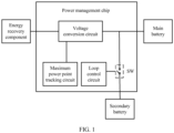
- FIG. 1 is an architecture diagram of a power management chip in the prior art.
- a voltage conversion circuit is connected to an energy recovery component, a maximum power point tracking circuit, a switch SW, and a main battery, and is configured to convert a voltage output by the energy recovery component.
- a loop control circuit is connected to the switch SW and is configured to receive a valid signal or an invalid signal. Specifically, a valid signal is received when a host is in an active state, and an invalid signal is received when the host is in an inactive state. The valid signal may control the switch SW to be closed, and the invalid signal may control the switch SW to be opened.
- the switch SW is connected to the voltage conversion circuit, a secondary battery, and the main battery, a control end of the switch SW is connected to the loop control circuit, and the switch SW is configured to connect or disconnect a channel between the secondary battery and both the voltage conversion circuit and the main battery.
- the loop control circuit receives a valid signal, and the valid signal controls the switch SW to be closed, so that the channel between the secondary battery and both the voltage conversion circuit and the main battery is connected, that is, output of the energy recovery component charges both the main battery and the secondary battery by using the voltage forwarding circuit, but cannot charge only the main battery.
- the power management chip in the prior art cannot preferably charge the main battery when the host is in an active state, that is, cannot ensure normal charging of dual batteries.
- a power management circuit according to claim 1, and an intelligent terminal according to claim 4 are provided, so that normal charging of dual batteries can be ensured. Further embodiments are provided in the dependent claims. Further embodiments of the description not falling under the scope of protection of the claims are provided for explanatory purpose only.
- control circuit may further include a third input end, a fourth input end, an inverter, a third switch module, and a comparator;
- the power management circuit may further include a maximum power point tracking circuit; and the maximum power point tracking circuit is connected to the output end of the comparator, and is configured to periodically configure a working voltage of the energy recovery component when receiving an enabling signal output by the comparator, so that the energy recovery component works at a maximum power output point, where the working voltage is configured by the maximum power point tracking circuit according to an open-circuit voltage of the energy recovery component and a preset algorithm.
- the activeness detection circuit may include a first resistor and a second resistor, and the first resistor and the second resistor are connected between a power end and a detection input end, where there are two leading wires between the first resistor and the second resistor, one leading wire is connected to a fifth output end, and the other leading wire is grounded by using a capacitor.
- the power management circuit configured a priority of dual-battery charging. Specific configuration is as follows:
- a circuit management circuit that meets the foregoing priority configuration may be implemented by using solutions of Embodiment 1 and Embodiment 2 of the present invention.
- FIG. 2 is a circuit diagram of a power management circuit according to Embodiment 1 of the present invention.
- the power management circuit includes a control circuit (Charger controller) 100, a first switch module 200, a second switch module 300, and a voltage conversion circuit (Boost Regulator) 400.
- Charger controller Charger controller
- Boost Regulator voltage conversion circuit
- the control circuit 100 includes a first input end I1, a second input end I2, a third input end I3, a fourth input end I4, a first output end O1, a second output end O2, and a third output end O3.
- the first input end I1 receives a main battery activeness detection signal Dect_active
- the second input end I2 receives a voltage signal of a secondary battery
- the third input end I3 receives a preset voltage signal Vref
- the fourth input end I4 receives a voltage division signal of a voltage division circuit.
- the first output end O1 is connected to an enabling end EN2 of the second switch module 300
- the second output end O2 is connected to an enabling end EN1 of the first switch module 200
- the third output end O3 is connected to the second switch module 300.
- the first switch module 200 is connected to the voltage conversion circuit 400, the secondary battery, and a main battery (Main Battery).
- the second switch module 300 is connected to the voltage conversion circuit 400 and an energy recovery component (Energy Source).
- Energy Source an energy recovery component
- the voltage conversion circuit 400 includes a fifth input end I5 and a fourth output end O4.
- the fifth input end I5 is connected to the second switch module 300.
- the fourth output end O4 has two leading wires, one leading wire is connected to the main battery, and the other leading wire is connected to the first switch module 200.
- the control circuit 100 controls the first switch module 200 to be opened or closed, and controls the enabling end EN2 of the second switch module 300 to input a signal or not to input a signal.
- the enabling end EN2 of the second switch module 300 does not input a signal, the second switch module 300 is in a state 13, that is, the second switch module 300 is in the state 13 by default.
- the enabling end EN2 of the second switch module 300 inputs a signal, and the input signal is a valid signal, the second switch module 300 is in a state 23.
- the input signal is an invalid signal, the second switch module 300 is also in the state 13.
- control circuit 100 controls the enabling end EN2 of the second switch module 300 to input or not to input a signal is described below.
- FIG. 3 is a structural diagram of a power management circuit according to Embodiment 2 of the present invention.
- a control circuit 100 in the power management circuit further includes an inverter 110, a third switch module 120, and a comparator 130.
- the inverter 110 is connected to a first input end I1, an enabling end EN3 of the third switch module 120, and a second output end O2, and is configured to control a first switch module 200 and the third switch module 120 to be in opposite states.
- the second output end O2 outputs the low-level signal
- an enabling end EN1 of the first switch module 200 receives the low-level signal
- the first switch module 200 is in an open state
- the low-level signal becomes a high-level signal after being converted by the inverter 110
- the enabling end EN3 of the third switch module 120 receives the high-level signal
- the third switch module 120 is in a closed state.
- the second output end O2 When the first input end I1 of the inverter 110 inputs a high-level signal, the second output end O2 outputs the high-level signal, the enabling end EN1 of the first switch module 200 receives the high-level signal, the first switch module 200 is in a closed state, the high-level signal becomes a low-level signal after being converted by the inverter 110, the enabling end EN3 of the third switch module 120 receives the low-level signal, and the third switch module 120 is in an open state.
- the third switch module 120 is connected to a first output end 01 and an output end of the comparator 130, and the enabling end EN3 of the third switch module 120 is connected to the inverter 110.
- the control circuit 100 controls, by using the third switch module 120, an enabling end EN2 of a second switch module 300 to input or not to input a signal.
- a channel between the enabling end EN2 of the second switch module and the output end of the comparator 130 may be connected, so that the enabling end EN2 of the second switch module 300 can input a signal, that is, the control circuit 100 can control the enabling end EN2 of the second switch module 300 to input a signal.
- the inverter 110 controls the third switch module 120 to be in an open state
- the channel between the enabling end EN2 of the second switch module and the output end of the comparator 130 is disconnected, so that the enabling end EN2 of the second switch module 300 does not input a signal, that is, the control circuit 100 can control the enabling end EN2 of the second switch module 300 not to input a signal.
- the comparator 130 is connected to a third input end I3, a fourth input end O4, and the third switch module 120, and is configured to: compare a voltage division signal of a voltage division circuit that is received by the fourth input end I4 with a preset voltage signal Vref received by the third input end I3, and control, according to a comparison result, a signal output by the first output end O1, so that the control circuit 100 can control the enabling end EN2 of the second switch module 300 to input a valid signal or an invalid signal.
- control circuit 100 controls the enabling end EN2 of the second switch module 300 to input or not to input a signal.
- An implementation in which the control circuit 100 controls the enabling end EN2 of the second switch module 300 to input a valid signal or an invalid signal when a signal is input is described below.
- the third switch module 120 when the third switch module 120 is in a closed state, that is, when the control circuit 100 controls the enabling end EN2 of the second switch module 300 to input a signal, and when the comparator 130 learns, by means of comparison, that a divided voltage of the voltage division circuit is higher than the Vref, the comparator 130 controls the first output end O1 to output a low-level signal, the low-level signal is a valid signal, the enabling end EN2 of the second switch module 300 receives the valid signal, and the second switch module 300 is in a state 23.
- the comparator 130 learns, by means of comparison, that the divided voltage of the voltage division circuit is not higher than the Vref, the comparator 130 controls the first output end O1 to output a low-level signal, the low-level signal is an invalid signal, the enabling end EN2 of the second switch module 300 receives the invalid signal, the invalid signal cannot play a control function, and the second switch module 300 returns to a default state 13.
- control circuit 100 may control, in another manner, the enabling end EN2 of the second switch module 300 to input a valid signal or an invalid signal when a signal is input.
- an analog-to-digital converter Analog-to-digital Converter, ADC
- the ADC is used to sample a voltage of the voltage division circuit
- the software is used to compare the voltage of the voltage division circuit with the preset voltage signal Vref, and to control, according to a comparison result, the enabling end EN2 of the second switch module 300 to input a low-level signal or a high-level signal, so as to control the enabling end EN2 of the second switch module 300 to input a valid signal or an invalid signal.
- the switch module mentioned in Embodiment 1 and Embodiment 2 of the present invention may be implemented by using a switch SW, or may be implemented by using a CMOS circuit, and this is not limited in the present invention.
- an energy recovery component is a component that can convert energy in another form in an environment into electric energy, for example, a component that can convert thermal energy, optical energy, mechanical vibration, and radio wave energy into electric energy.
- a main battery is disposed on a host.
- the host in this specification further includes a micro control unit (Micro Control Unit, MCU), an activeness detection circuit, Bluetooth, and the like, and can support an activeness detection function by using a contact.
- MCU Micro Control Unit
- a main battery activeness detection signal Dect_active is received by the control circuit 100 from the activeness detection circuit by using the first input end I1, the activeness detection circuit includes a fifth output end O5, and the fifth output end O5 is connected to the first input end I1.
- the activeness detection circuit is configured to detect whether the host is in an active state. When it is detected that the host is in an active state, a valid detection signal Dect_active is output by using the fifth output end O5. When it is detected that the host is in an inactive state, an invalid detection signal Dect_active is output by using the fifth output end O5.
- the valid detection signal Dect_active may be a low-level signal, and the invalid detection signal Dect_active may be a high-level signal.
- the control circuit 100 controls the second output end O2 to output the high-level signal, that is, the enabling end EN1 of the first switch module 200 receives the high-level signal, and the first switch module 200 is in a closed state.
- the control circuit 100 controls the first output end O1 to output a low-level signal, and controls, by using the low-level signal, the enabling end EN2 of the second switch module 300 not to input a signal.
- the second switch module 300 when the enabling end EN2 of the second switch module 300 does not input a signal, the second switch module 300 is in the state 13 by default, that is, a channel between the energy recovery component and the voltage conversion circuit is connected. In this case, a voltage signal output by the energy recovery component reaches the fifth input end I5 of the voltage conversion circuit 400 through the second switch module 300.
- the voltage conversion circuit 400 converts the voltage signal (for example, converts a low voltage output by the energy recovery component into a target voltage), and outputs the converted voltage signal to the secondary battery by using the fourth output end O4. In this way, the energy recovery component charges the secondary battery.
- the activeness detection circuit detects that the host is inactive, that is, the voltage conversion circuit 400 is disconnected from the main battery, the invalid detection signal Dect_active is output by using the fifth output end O5, that is, the control circuit 100 receives the invalid detection signal Dect_active by using the first input end I1. Therefore, after converting the voltage signal output by the energy recovery component, the voltage conversion circuit 400 directly outputs the voltage signal to the secondary battery by using the fourth output end O4.
- the control circuit 100 controls the second output end O2 to output the low-level signal, that is, the enabling end EN1 of the first switch module 200 receives the low-level signal, and the first switch module 200 is in an open state.
- the control circuit 100 controls the first output end O1 to output a high-level signal, and controls, by using the high-level signal, the enabling end EN2 of the second switch module 300 to input a signal.
- the valid signal controls the second switch module 300 to be in the state 23, that is, a channel between the control circuit and the voltage conversion circuit is connected.
- the control circuit 100 controls the third output end O3 to output the voltage signal.
- the voltage signal reaches the fifth input end I5 of the voltage conversion circuit 400 through the second switch module 300.
- the voltage conversion circuit 400 converts the voltage signal (for example, converts a low voltage output by the secondary battery into a target voltage), and outputs the converted voltage signal to the main battery by using the fourth output end O4. In this way, the main battery charges the secondary battery.
- the second switch module 300 when the enabling end EN2 of the second switch module 300 inputs a signal and the input signal is an invalid signal, because the invalid signal cannot play a control function, the second switch module 300 is in the default state 13, that is, a channel between the energy recovery component and the voltage conversion circuit is connected. In this case, a voltage signal output by the energy recovery component reaches the fifth input end I5 of the voltage conversion circuit 400 through the second switch module 300.
- the voltage conversion circuit 400 converts the voltage signal (for example, converts a low voltage output by the energy recovery component into a target voltage), and outputs the converted voltage signal to the main battery by using the fourth output end O4. In this way, the energy recovery component charges the main battery.
- the voltage conversion circuit 400 after converting the voltage signal output by the energy recovery component, the voltage conversion circuit 400 directly outputs the voltage signal to the main battery by using the fourth output end O4 because when the first switch module 200 is in an open state, the fourth output end O4 of the voltage conversion circuit 400 is connected only to the main battery.
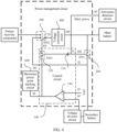
- FIG. 4 is a structural diagram of a power management circuit according to Embodiment 3 of the present invention. As shown in FIG. 4 , the power management circuit further includes a maximum power point tracking circuit (Maximum Power Point Tracking Controller) 600.
- a maximum power point tracking circuit Maximum Power Point Tracking Controller 600.
- the maximum power point tracking circuit 600 includes a sixth input end I6, and the sixth input end I6 is connected to an output end of a comparator 130.
- the sixth input end I6 of the maximum power point tracking circuit 600 inputs an enabling signal, and the enabling signal may be a valid signal output by the comparator 110 in FIG. 3 by using the output end when the comparator 110 learns, by means of comparison, that the divided voltage of the voltage division circuit is higher than the Vref.
- the maximum power point tracking circuit 600 when receiving the enabling signal output by the output end of the comparator 110, the maximum power point tracking circuit 600 periodically configures a working voltage of an energy recovery component, so that the energy recovery component works at a maximum power output point.
- the working voltage is configured by the maximum power point tracking circuit according to an open-circuit voltage of the energy recovery component and a preset algorithm.
- the maximum power point tracking circuit 600 periodically performs the following steps according to a characteristic of the energy recovery component: first, setting a voltage conversion circuit to a stop state; then sampling the open-circuit voltage of the energy recovery component, and configuring the working voltage of the energy recovery component according to the preset algorithm, so that the energy recovery component works at the maximum power output point; and finally, starting the voltage conversion circuit 400.
- control circuit 100 in the present invention can control a loop of charging currents of dual batteries, such as controlling opening and closing of the first switch module, the second switch module, and the third switch module, and implement an under-voltage protection (Under-Voltage Protection, UVP) function and an overvoltage protection (Overvoltage Protection, OVP) function for dual-battery charging.
- the control circuit 100 is further configured to perform enabling control on the maximum power point tracking circuit. In this way, when a voltage of the secondary battery is lower than a voltage of the main battery, the main battery can still be charged.
- FIG. 5 is a circuit diagram of an intelligent terminal according to an embodiment of the present invention.
- the intelligent terminal includes a host and a receptacle (such as a wrist strap) that can be separated from the host.
- the host includes a main battery and an activeness detection circuit
- the receptacle includes an energy recovery component, a secondary battery, and the power management circuit in the foregoing Embodiment 1, Embodiment 2, or Embodiment 3.
- the activeness detection circuit includes a first resistor R1 and a second resistor R2. Specifically, the first resistor R1 and the second resistor R2 are connected between a power end VDD and a detection input end. There are two leading wires between the first resistor R1 and the second resistor R2, one leading wire is connected to a fifth output end O5, and the other leading wire is grounded by using a capacitor.
- the capacitor herein has functions of voltage regulation and filtering, that is, the capacitor can ensure that the fifth output end O5 outputs a stable main battery activeness detection signal Dect_active.
- the detection input end when the host is inactive, the detection input end does not input a signal, and a voltage signal output by the fifth output end O5 is pulled up to the VDD by the first resistor R1, that is, the fifth output end O5 outputs an invalid detection signal.
- the detection input end When the host is active, the detection input end is grounded, that is, the detection input end, the first resistor R1, the second resistor R2, and the VDD form a loop, or that is, the first resistor R1 and the second resistor R2 divides a voltage of the VDD, so that the voltage signal output by the fifth output end O5 is not equal to the VDD, that is, the fifth output end O5 outputs a valid detection signal.
- the activeness detection circuit may be implemented by using another circuit, such as a capacitor, a Hall component, or a heart rate sensor, and this is not limited in the present invention.
- the activeness detection circuit is implemented by using a capacitor.
- capacitance of the capacitor changes. Therefore, whether the host is active can be detected by detecting the capacitance of the capacitor.
- the receptacle in FIG. 5 may further include a voltage division circuit, and the voltage division circuit includes a first voltage division resistor R3 and a second voltage division resistor R4.
- the first voltage division resistor R3 and the second voltage division resistor R4 are connected between a grounded end and the secondary battery.
- a voltage signal obtained after a voltage of the secondary battery is divided by the first voltage division resistor R3 and the second voltage division resistor R4 is input to a comparator 110 by using the fourth input end I4.
- the comparator 110 compares a voltage division voltage of the first voltage division resistor R3 with Vref, and controls, according to a comparison result, a signal output by a first output end O1.
- a method for controlling, according to the comparison result, the signal output by the first output end O1 is described in Embodiment 2 of the present invention, and details are not described herein again.
- Vref V1 ⁇ (R3 / R3 + R4).
- V1 is a threshold voltage corresponding to a preset remaining power threshold A of the secondary battery, and the remaining power threshold A of the secondary battery may be set according to a material of the secondary battery, for example, may be set to 80% or 50%.
- remaining power of the secondary battery is calculated by determining the voltage of the secondary battery.
- resistance of the R3 and resistance of the R4 may be adjusted according to the preset voltage signal Vref.
- the intelligent terminal compares the voltage of the voltage division circuit and the preset voltage signal Vref, that is, determines a relationship between the remaining power of the secondary battery and the remaining power threshold A.
- the remaining power of the secondary battery is higher than the remaining power threshold A, a channel used by the secondary battery to charge the main battery is connected and an enabling signal is output.
- the remaining power of the secondary battery is not higher than the remaining power threshold A, the channel used by the secondary battery to charge the main battery is disconnected.
- the intelligent terminal provided in this embodiment of the present invention may be a smart band, a smart watch, a smart hat, or the like that uses an energy recovery technology and that has dual batteries, and can implement, by using the voltage division circuit, a function of charging the main battery when the voltage of the secondary battery is lower than the voltage of the main battery. Therefore, charging efficiency of the intelligent terminal is improved.
- FIG. 7 is a flowchart of a charging method of a power management circuit according to Embodiment 4 of the present invention.
- the charging method provided in this embodiment of the present invention is based on the power management circuit described in the foregoing embodiments.
- the charging method of the power management circuit in this embodiment of the present invention specifically includes the following steps.
- Step 701 A first input end receives a main battery activeness detection signal.
- a first input end of a control circuit receives a main battery activeness detection signal Dect_active of an activeness detection circuit.
- the activeness detection circuit is configured to: detect whether a host is in an active state, and output a valid detection signal Dect_active when detecting that the host is in an active state, or output an invalid detection signal Dect_active when detecting that the host is in an inactive state.
- the valid detection signal Dect_active may be a low-level signal
- the invalid detection signal Dect_active may be a high-level signal.
- Step 702 Connect, according to the main battery activeness detection signal, a channel used by an energy recovery component to charge a secondary battery, or connect, according to the main battery activeness detection signal, a channel used by an energy recovery component or a secondary battery to charge a main battery.
- the energy recovery component is a component that can convert energy in another form in an environment into electric energy, for example, a component that can convert thermal energy, optical energy, mechanical vibration, and radio wave energy into electric energy.
- step 702 when the received main battery activeness detection signal is an invalid detection signal, the channel used by the energy recovery component to charge the secondary battery is connected, and when the received main battery activeness detection signal is a valid detection signal, the channel used by the secondary battery or the energy recovery component to charge the main battery is connected.
- the main battery when the host is in an active state, the main battery can be preferably charged, so as to ensure normal charging of dual batteries.
- Steps of methods or algorithms described in the embodiments disclosed in this specification may be implemented by hardware, a software module executed by a processor, or a combination thereof.
- the software module may reside in a random access memory (RAM), a memory, a read-only memory (ROM), an electrically programmable ROM, an electrically erasable programmable ROM, a register, a hard disk, a removable disk, a CD-ROM, or any other form of storage medium known in the art.
Landscapes
- Engineering & Computer Science (AREA)
- Power Engineering (AREA)
- Charge And Discharge Circuits For Batteries Or The Like (AREA)
- Secondary Cells (AREA)
Claims (5)
- Leistungsmanagementschaltung, wobei die Leistungsmanagementschaltung eine Steuerschaltung (100), ein erstes Schaltmodul (200), ein zweites Schaltmodul (300) und eine Spannungswandlungsschaltung (400) umfasst;wobei die Steuerschaltung ein erstes Eingangsende (11), ein erstes Ausgangsende (O1), ein zweites Eingangsende (I2), ein zweites Ausgangsende (O2) und ein drittes Ausgangsende (O3) umfasst,wobei das erste Eingangsende dazu konfiguriert ist, ein Hauptbatterieaktivitätserkennungssignal zu empfangen, wobei das erste Ausgangsende mit einem Freigabeende des zweiten Schaltmoduls verbunden ist, das zweite Ausgangsende mit einem Freigabeende des ersten Schaltmoduls verbunden ist, das zweite Eingangsende dazu konfiguriert ist, mit einer Sekundärbatterie verbunden zu sein, und das dritte Ausgangsende mit dem zweiten Schaltmodul verbunden ist,wobeidas durch die Steuerschaltung empfangene Hauptbatterieaktivitätserkennungssignal ein ungültiges Erkennungssignal ist, wenn die Spannungswandlungsschaltung von einer Hauptbatterie getrennt ist, und wobei das durch die Steuerschaltung empfangene Hauptbatterieaktivitätserkennungssignal ein gültiges Erkennungssignal ist, wenn die Spannungswandlungsschaltung mit der Hauptbatterie verbunden ist;wobei das erste Schaltmodul mit der Spannungswandlungsschaltung, der Sekundärbatterie und der Hauptbatterie verbindbar ist;wobei das zweite Schaltmodul mit der Spannungswandlungsschaltung und einer Energierückgewinnungskomponente verbindbar ist; undwobei, entsprechend dem empfangenen Hauptbatterieaktivitätserkennungssignal, die Steuerschaltung dazu konfiguriert ist, das erste Schaltmodul so zu steuern, dass es geschlossen oder geöffnet wird, und das zweite Schaltmodul so zu steuern, dass es kein Signal eingibt, ein gültiges Signal eingibt oder ein ungültiges Signal eingibt, so dass ein durch die Energierückgewinnungskomponente zum Laden der Sekundärbatterie verwendeter Kanal verbunden wird oder ein durch die Sekundärbatterie oder die Energierückgewinnungskomponente zum Laden der Hauptbatterie verwendeter Kanal verbunden wird, wobeiwenn das durch die Steuerschaltung empfangene Hauptbatterieaktivitätserkennungssignal das ungültige Erkennungssignal ist, die Steuerschaltung dazu konfiguriert ist, das erste Schaltmodul so zu steuern, dass es geschlossen wird, und das Freigabeende des zweiten Schaltmoduls so zu steuern, dass es kein Signal eingibt; undwenn das Freigabeende des zweiten Schaltmoduls kein Signal eingibt, sich das zweite Schaltmodul in einem ersten Zustand befindet, ein Kanal zwischen der Energierückgewinnungskomponente und der Spannungswandlungsschaltung verbunden wird und die Spannungswandlungsschaltung dazu konfiguriert ist, ein von der Energierückgewinnungskomponente empfangenes Spannungssignal umzuwandeln und das Spannungssignal an die Sekundärbatterie auszugeben, so dass der durch die Energierückgewinnungskomponente zum Laden der Sekundärbatterie verwendete Kanal verbunden wird, wobeiwenn das durch die Steuerschaltung empfangene Hauptbatterieaktivitätserkennungssignal das gültige Erkennungssignal ist, die Steuerschaltung dazu konfiguriert ist, das erste Schaltmodul so zu steuern, dass es geöffnet wird, und das Freigabeende des zweiten Schaltmoduls so zu steuern, dass es ein gültiges Signal eingibt; undwenn das Freigabeende des zweiten Schaltmoduls ein gültiges Signal eingibt, sich das zweite Schaltmodul in einem zweiten Zustand befindet, ein Kanal zwischen der Steuerschaltung und der Spannungswandlungsschaltung verbunden wird und die Spannungswandlungsschaltung dazu konfiguriert ist, ein von der Sekundärbatterie über die Steuerschaltung empfangenes Spannungssignal umzuwandeln und das Spannungssignal an die Hauptbatterie auszugeben, so dass der durch die Sekundärbatterie zum Laden der Hauptbatterie verwendete Kanal verbunden wird.
- Leistungsmanagementschaltung nach Anspruch 1, wobei die Steuerschaltung ferner ein drittes Eingangsende, ein viertes Eingangsende, einen Umrichter, ein drittes Schaltmodul und einen Komparator umfasst;wobei das dritte Eingangsende dazu konfiguriert ist, ein voreingestelltes Spannungssignal zu empfangen, und das vierte Eingangsende dazu konfiguriert ist, ein Spannungsteilungssignal einer Spannungsteilungsschaltung zu empfangen;wobei der Umrichter mit dem ersten Eingangsende, einem Freigabeende des dritten Schaltmoduls und dem zweiten Ausgangsende verbunden ist und dazu konfiguriert ist, das erste Schaltmodul und das dritte Schaltmodul so zu steuern, dass sie sich in entgegengesetzten Zuständen befinden;wobei das dritte Schaltmodul mit dem ersten Ausgangsende und einem Ausgangsende des Komparators verbunden ist, und das Freigabeende des dritten Schaltmoduls mit dem Umrichter verbunden ist;wobei der Komparator mit dem dritten Eingangsende, dem vierten Eingangsende und dem dritten Schaltmodul verbunden ist und dazu konfiguriert ist, das empfangene Spannungsteilungssignal der Spannungsteilungsschaltung mit dem empfangenen voreingestellten Spannungssignal zu vergleichen;wobei, wenn der Umrichter dazu konfiguriert ist, das dritte Schaltmodul so zu steuern, dass es sich in einem geöffneten Zustand befindet, ein Kanal zwischen dem Freigabeende des zweiten Schaltmoduls und dem Ausgangsende des Komparators getrennt wird, so dass das Freigabeende des zweiten Schaltmoduls so gesteuert wird, dass es kein Signal eingibt;wobei, wenn der Umrichter dazu konfiguriert ist, das dritte Schaltmodul so zu steuern, dass es sich in einem geschlossenen Zustand befindet, ein Kanal zwischen dem Freigabeende des zweiten Schaltmoduls und dem Ausgangsende des Komparators verbunden wird, so dass das Freigabeende des zweiten Schaltmoduls so gesteuert wird, dass es ein Signal eingibt; undwobei, wenn das Freigabeende des zweiten Schaltmoduls ein Signal eingibt, und wenn der Komparator mittels eines Vergleichs herausfindet, dass das Spannungsteilungssignal der Spannungsteilungsschaltung höher als das voreingestellte Spannungssignal ist, der Komparator dazu konfiguriert ist, das erste Ausgangsende so zu steuern, dass es ein gültiges Signal ausgibt, um das Freigabeende des zweiten Schaltmoduls so zu steuern, dass es das gültige Signal eingibt; oder wobei, wenn der Komparator mittels eines Vergleichs herausfindet, dass das Spannungsteilungssignal der Spannungsteilungsschaltung nicht höher als das voreingestellte Spannungssignal ist, der Komparator dazu konfiguriert ist, das erste Ausgangsende so zu steuern, dass es ein ungültiges Signal ausgibt, um das Freigabeende des zweiten Schaltmoduls so zu steuern, dass es das ungültige Signal eingibt.
- Leistungsmanagementschaltung nach Anspruch 2, wobei die Leistungsmanagementschaltung ferner eine Maximalleistungspunktnachverfolgungsschaltung umfasst; und
wobei die Maximalleistungspunktnachverfolgungsschaltung mit dem Ausgangsende des Komparators verbunden ist und dazu konfiguriert ist, eine Arbeitsspannung der Energierückgewinnungskomponente periodisch zu konfigurieren, wenn ein Freigabesignalausgang durch den Komparator empfangen wird, so dass die Energierückgewinnungskomponente bei einem Maximalleistungsausgabepunkt arbeitet, wobei die Arbeitsspannung durch die Maximalleistungspunktnachverfolgungsschaltung entsprechend einer Leerlaufspannung der Energierückgewinnungskomponente und einem voreingestellten Algorithmus konfiguriert wird. - Intelligentes Endgerät, wobei das intelligente Endgerät einen Host und eine Aufnahme umfasst, die von dem Host getrennt werden kann, wobei der Host eine Hauptbatterie und eine Aktivitätserkennungsschaltung umfasst, und die Aufnahme eine Energierückgewinnungskomponente, eine Sekundärbatterie und die Leistungsmanagementschaltung nach einem der Ansprüche 1 bis 3 umfasst; und
wobei die Aktivitätserkennungsschaltung mit dem ersten Eingangsende verbunden ist und zu Folgendem konfiguriert ist: Erkennen, ob sich der Host in einem aktiven Zustand befindet, und Ausgeben eines gültigen Erkennungssignals bei Erkennen, dass sich der Host in einem aktiven Zustand befindet, oder Ausgeben eines ungültigen Erkennungssignals bei Erkennen, dass sich der Host in einem inaktiven Zustand befindet. - Intelligentes Endgerät nach Anspruch 4, wobei die Aktivitätserkennungsschaltung einen ersten Widerstand und einen zweiten Widerstand umfasst, und der erste Widerstand und der zweite Widerstand zwischen einem Leistungsende und einem Erkennungseingangsende verbunden sind, wobei zwei Leitungsdrähte zwischen dem ersten Widerstand und dem zweiten Widerstand vorhanden sind, wobei ein Leitungsdraht mit einem fünften Ausgangsende verbunden ist und der andere Leitungsdraht unter Verwendung eines Kondensators geerdet ist.
Applications Claiming Priority (2)
| Application Number | Priority Date | Filing Date | Title |
|---|---|---|---|
| CN201510559299.9A CN106487055B (zh) | 2015-09-02 | 2015-09-02 | 电源管理电路、智能终端及充电方法 |
| PCT/CN2016/097828 WO2017036413A1 (zh) | 2015-09-02 | 2016-09-01 | 电源管理电路、智能终端及充电方法 |
Publications (3)
| Publication Number | Publication Date |
|---|---|
| EP3337003A1 EP3337003A1 (de) | 2018-06-20 |
| EP3337003A4 EP3337003A4 (de) | 2018-09-05 |
| EP3337003B1 true EP3337003B1 (de) | 2024-03-20 |
Family
ID=58186712
Family Applications (1)
| Application Number | Title | Priority Date | Filing Date |
|---|---|---|---|
| EP16840842.5A Active EP3337003B1 (de) | 2015-09-02 | 2016-09-01 | Leistungsverwaltungsschaltung, intelligentes endgerät und ladeverfahren |
Country Status (4)
| Country | Link |
|---|---|
| US (1) | US11005273B2 (de) |
| EP (1) | EP3337003B1 (de) |
| CN (1) | CN106487055B (de) |
| WO (1) | WO2017036413A1 (de) |
Families Citing this family (20)
| Publication number | Priority date | Publication date | Assignee | Title |
|---|---|---|---|---|
| CN108288866A (zh) * | 2018-03-19 | 2018-07-17 | 西安九天无限智能科技有限公司 | 一种应用在ar智能眼镜上的双电池管理系统 |
| CN109038835B (zh) * | 2018-06-21 | 2020-09-15 | 佛山市顺德区中山大学研究院 | 一种具有最大功率点跟踪功能的微能量采集电路 |
| CN110764398B (zh) * | 2018-07-26 | 2021-06-01 | 青岛海信移动通信技术股份有限公司 | 一种智能手表及其模式切换方法 |
| WO2020020356A1 (zh) * | 2018-07-26 | 2020-01-30 | 青岛海信移动通信技术股份有限公司 | 智能手表及其模式切换方法 |
| CN110764397B (zh) * | 2018-07-26 | 2021-07-23 | 青岛海信移动通信技术股份有限公司 | 一种智能手表及其模式切换方法 |
| TWI709032B (zh) * | 2018-09-19 | 2020-11-01 | 中原大學 | 智慧型獵能裝置、電壓訊號應用系統及其能源管理模組 |
| CN109217425A (zh) * | 2018-10-16 | 2019-01-15 | 深圳市联讯发科技有限公司 | 一种充电器电路及其智能充电控制方法 |
| EP4018527B1 (de) * | 2019-10-17 | 2025-08-13 | Samsung Electronics Co., Ltd. | Elektronische vorrichtung, die eine resonanzladeschaltung einschliesst |
| WO2021075916A1 (en) | 2019-10-17 | 2021-04-22 | Samsung Electronics Co., Ltd. | Electronic device including resonant charging circuit |
| CN111934276A (zh) * | 2020-08-11 | 2020-11-13 | 广东电网有限责任公司 | 用于局放检测装置的供电系统及其供电方法 |
| CN111987787B (zh) * | 2020-08-28 | 2022-07-26 | 北京航空航天大学 | 一种能量可回收水下航行器的电源管理系统 |
| CN111938759B (zh) * | 2020-09-04 | 2025-06-17 | 盈甲医疗器械制造(上海)有限公司 | 具有可同时按压的刀头按钮的超声外科器械 |
| CN112448462A (zh) * | 2020-11-19 | 2021-03-05 | 深圳奥尼电子股份有限公司 | 电源管理电路、电源管理方法及电子设备 |
| CN113346888A (zh) * | 2021-07-08 | 2021-09-03 | 凌矽电子科技(东莞)有限公司 | 一种无线开关装置及其控制方法 |
| CN113595188B (zh) * | 2021-07-28 | 2023-06-23 | 中国人民解放军陆军工程大学 | 多能源模式的电池充电路由器 |
| CN113725995B (zh) * | 2021-08-24 | 2024-01-02 | 南京南瑞继保电气有限公司 | 一种配电终端双后备电源管理系统及其管理方法 |
| CN115640184B (zh) * | 2022-11-04 | 2026-02-27 | 济南浪潮数据技术有限公司 | 一种服务器开机故障检测装置、方法及服务器 |
| CN116231821A (zh) * | 2022-12-27 | 2023-06-06 | 熵基科技股份有限公司 | 一种电能回收电路、电能回收装置、电子设备 |
| CN116566197B (zh) * | 2023-05-09 | 2024-04-09 | 广州市依歌智能科技有限公司 | 一种智能窗口导通取电芯片、供电电路 |
| CN118659484B (zh) * | 2024-05-30 | 2025-02-11 | 嘉兴致芯科技有限公司 | 一种自适应动能量回收控制电路和方法 |
Family Cites Families (10)
| Publication number | Priority date | Publication date | Assignee | Title |
|---|---|---|---|---|
| JP2986059B2 (ja) | 1995-03-08 | 1999-12-06 | インターナショナル・ビジネス・マシーンズ・コーポレイション | バッテリ充電装置 |
| JP2000324719A (ja) * | 1999-05-17 | 2000-11-24 | Canon Inc | 電子機器、その制御方法および記憶媒体 |
| KR100536589B1 (ko) * | 1999-07-27 | 2005-12-14 | 삼성전자주식회사 | 배터리 전원의 전자 장치 및 그의 전원 공급 제어 방법 |
| JP2008048473A (ja) | 2006-08-10 | 2008-02-28 | Sanyo Electric Co Ltd | 充電器 |
| CN101388555B (zh) | 2007-09-14 | 2011-08-03 | 联想移动通信科技有限公司 | 一种便携设备的智能扩展电源系统 |
| CN101867198B (zh) * | 2009-04-20 | 2012-11-28 | 龙旗科技(上海)有限公司 | 一种手机备用电池的实现装置和控制方法 |
| CN101789690B (zh) * | 2010-01-26 | 2011-12-14 | 山特电子(深圳)有限公司 | 一种ups前级升压装置 |
| US8405360B2 (en) * | 2010-04-07 | 2013-03-26 | Evp Technology Llc Usa | Energy-efficient fast charging device and method |
| CN101997327A (zh) * | 2010-12-07 | 2011-03-30 | 东莞市钜大电子有限公司 | 便携式智能锂电池充电器 |
| CN103227502A (zh) | 2013-04-07 | 2013-07-31 | 无锡职业技术学院 | 一种智能电池 |
-
2015
- 2015-09-02 CN CN201510559299.9A patent/CN106487055B/zh active Active
-
2016
- 2016-09-01 WO PCT/CN2016/097828 patent/WO2017036413A1/zh not_active Ceased
- 2016-09-01 US US15/756,985 patent/US11005273B2/en active Active
- 2016-09-01 EP EP16840842.5A patent/EP3337003B1/de active Active
Also Published As
| Publication number | Publication date |
|---|---|
| EP3337003A4 (de) | 2018-09-05 |
| CN106487055B (zh) | 2019-06-11 |
| CN106487055A (zh) | 2017-03-08 |
| US20180248387A1 (en) | 2018-08-30 |
| EP3337003A1 (de) | 2018-06-20 |
| US11005273B2 (en) | 2021-05-11 |
| WO2017036413A1 (zh) | 2017-03-09 |
Similar Documents
| Publication | Publication Date | Title |
|---|---|---|
| US11005273B2 (en) | Power management circuit, intelligent terminal, and charging method | |
| US9673643B2 (en) | Battery presence detecting method, apparatus and charging system | |
| JP6323727B2 (ja) | 太陽電池用給電器及び太陽電池システム | |
| US20100207571A1 (en) | Solar chargeable battery for portable devices | |
| CN103607009B (zh) | 一种带自动保护功能的充放电电路 | |
| JP6669931B2 (ja) | 高速充電方法及びシステム、端末並びに充電器 | |
| CN112531825B (zh) | 一种电池保护电路及电池充放电电路 | |
| JP7350164B2 (ja) | 電子デバイス、充電方法、および充電システム | |
| US10312701B2 (en) | Charging method and portable electronic device using the same | |
| JP2017099151A (ja) | 制御装置、受電装置、電子機器及び無接点電力伝送システム | |
| CN118747028B (zh) | 供电选择电路、芯片及电子设备 | |
| CN114914967B (zh) | 充电盒电路、无线耳机以及无线耳机系统 | |
| CN106712167A (zh) | 一种充电电源保护设备 | |
| CN116388350B (zh) | 充电控制方法、储能设备和可读存储介质 | |
| JP2011091901A (ja) | バッテリ状態監視回路及びバッテリ装置 | |
| WO2017117400A1 (en) | Modular battery system | |
| US9153992B2 (en) | High-temperature resistant power bank circuit | |
| CN105337340A (zh) | 兼容镍氢电池和锂电池的三段式充电电路 | |
| CN204597597U (zh) | 一种家用太阳能供电系统 | |
| CN211046538U (zh) | 充电装置 | |
| JP6880547B2 (ja) | 無接点電力伝送システム | |
| US12587026B2 (en) | Dynamically selectable power and charging configurations | |
| WO2012102933A2 (en) | Detection of insufficient supplied power | |
| CN104810898A (zh) | 一种家用太阳能供电系统及其控制方法 | |
| CN205195315U (zh) | 兼容镍氢电池和锂电池的三段式充电电路 |
Legal Events
| Date | Code | Title | Description |
|---|---|---|---|
| STAA | Information on the status of an ep patent application or granted ep patent |
Free format text: STATUS: THE INTERNATIONAL PUBLICATION HAS BEEN MADE |
|
| PUAI | Public reference made under article 153(3) epc to a published international application that has entered the european phase |
Free format text: ORIGINAL CODE: 0009012 |
|
| STAA | Information on the status of an ep patent application or granted ep patent |
Free format text: STATUS: REQUEST FOR EXAMINATION WAS MADE |
|
| 17P | Request for examination filed |
Effective date: 20180312 |
|
| AK | Designated contracting states |
Kind code of ref document: A1 Designated state(s): AL AT BE BG CH CY CZ DE DK EE ES FI FR GB GR HR HU IE IS IT LI LT LU LV MC MK MT NL NO PL PT RO RS SE SI SK SM TR |
|
| AX | Request for extension of the european patent |
Extension state: BA ME |
|
| A4 | Supplementary search report drawn up and despatched |
Effective date: 20180807 |
|
| RIC1 | Information provided on ipc code assigned before grant |
Ipc: H02J 7/00 20060101AFI20180801BHEP |
|
| DAV | Request for validation of the european patent (deleted) | ||
| DAX | Request for extension of the european patent (deleted) | ||
| STAA | Information on the status of an ep patent application or granted ep patent |
Free format text: STATUS: EXAMINATION IS IN PROGRESS |
|
| 17Q | First examination report despatched |
Effective date: 20200114 |
|
| GRAP | Despatch of communication of intention to grant a patent |
Free format text: ORIGINAL CODE: EPIDOSNIGR1 |
|
| STAA | Information on the status of an ep patent application or granted ep patent |
Free format text: STATUS: GRANT OF PATENT IS INTENDED |
|
| INTG | Intention to grant announced |
Effective date: 20231122 |
|
| GRAS | Grant fee paid |
Free format text: ORIGINAL CODE: EPIDOSNIGR3 |
|
| GRAA | (expected) grant |
Free format text: ORIGINAL CODE: 0009210 |
|
| STAA | Information on the status of an ep patent application or granted ep patent |
Free format text: STATUS: THE PATENT HAS BEEN GRANTED |
|
| AK | Designated contracting states |
Kind code of ref document: B1 Designated state(s): AL AT BE BG CH CY CZ DE DK EE ES FI FR GB GR HR HU IE IS IT LI LT LU LV MC MK MT NL NO PL PT RO RS SE SI SK SM TR |
|
| REG | Reference to a national code |
Ref country code: GB Ref legal event code: FG4D |
|
| REG | Reference to a national code |
Ref country code: CH Ref legal event code: EP |
|
| REG | Reference to a national code |
Ref country code: IE Ref legal event code: FG4D |
|
| REG | Reference to a national code |
Ref country code: DE Ref legal event code: R096 Ref document number: 602016086459 Country of ref document: DE |
|
| PG25 | Lapsed in a contracting state [announced via postgrant information from national office to epo] |
Ref country code: LT Free format text: LAPSE BECAUSE OF FAILURE TO SUBMIT A TRANSLATION OF THE DESCRIPTION OR TO PAY THE FEE WITHIN THE PRESCRIBED TIME-LIMIT Effective date: 20240320 |
|
| REG | Reference to a national code |
Ref country code: LT Ref legal event code: MG9D |
|
| PG25 | Lapsed in a contracting state [announced via postgrant information from national office to epo] |
Ref country code: GR Free format text: LAPSE BECAUSE OF FAILURE TO SUBMIT A TRANSLATION OF THE DESCRIPTION OR TO PAY THE FEE WITHIN THE PRESCRIBED TIME-LIMIT Effective date: 20240621 |
|
| PG25 | Lapsed in a contracting state [announced via postgrant information from national office to epo] |
Ref country code: RS Free format text: LAPSE BECAUSE OF FAILURE TO SUBMIT A TRANSLATION OF THE DESCRIPTION OR TO PAY THE FEE WITHIN THE PRESCRIBED TIME-LIMIT Effective date: 20240620 Ref country code: HR Free format text: LAPSE BECAUSE OF FAILURE TO SUBMIT A TRANSLATION OF THE DESCRIPTION OR TO PAY THE FEE WITHIN THE PRESCRIBED TIME-LIMIT Effective date: 20240320 |
|
| REG | Reference to a national code |
Ref country code: NL Ref legal event code: MP Effective date: 20240320 |
|
| PG25 | Lapsed in a contracting state [announced via postgrant information from national office to epo] |
Ref country code: RS Free format text: LAPSE BECAUSE OF FAILURE TO SUBMIT A TRANSLATION OF THE DESCRIPTION OR TO PAY THE FEE WITHIN THE PRESCRIBED TIME-LIMIT Effective date: 20240620 Ref country code: NO Free format text: LAPSE BECAUSE OF FAILURE TO SUBMIT A TRANSLATION OF THE DESCRIPTION OR TO PAY THE FEE WITHIN THE PRESCRIBED TIME-LIMIT Effective date: 20240620 Ref country code: LT Free format text: LAPSE BECAUSE OF FAILURE TO SUBMIT A TRANSLATION OF THE DESCRIPTION OR TO PAY THE FEE WITHIN THE PRESCRIBED TIME-LIMIT Effective date: 20240320 Ref country code: HR Free format text: LAPSE BECAUSE OF FAILURE TO SUBMIT A TRANSLATION OF THE DESCRIPTION OR TO PAY THE FEE WITHIN THE PRESCRIBED TIME-LIMIT Effective date: 20240320 Ref country code: GR Free format text: LAPSE BECAUSE OF FAILURE TO SUBMIT A TRANSLATION OF THE DESCRIPTION OR TO PAY THE FEE WITHIN THE PRESCRIBED TIME-LIMIT Effective date: 20240621 Ref country code: FI Free format text: LAPSE BECAUSE OF FAILURE TO SUBMIT A TRANSLATION OF THE DESCRIPTION OR TO PAY THE FEE WITHIN THE PRESCRIBED TIME-LIMIT Effective date: 20240320 Ref country code: BG Free format text: LAPSE BECAUSE OF FAILURE TO SUBMIT A TRANSLATION OF THE DESCRIPTION OR TO PAY THE FEE WITHIN THE PRESCRIBED TIME-LIMIT Effective date: 20240320 |
|
| REG | Reference to a national code |
Ref country code: AT Ref legal event code: MK05 Ref document number: 1668694 Country of ref document: AT Kind code of ref document: T Effective date: 20240320 |
|
| PG25 | Lapsed in a contracting state [announced via postgrant information from national office to epo] |
Ref country code: SE Free format text: LAPSE BECAUSE OF FAILURE TO SUBMIT A TRANSLATION OF THE DESCRIPTION OR TO PAY THE FEE WITHIN THE PRESCRIBED TIME-LIMIT Effective date: 20240320 Ref country code: LV Free format text: LAPSE BECAUSE OF FAILURE TO SUBMIT A TRANSLATION OF THE DESCRIPTION OR TO PAY THE FEE WITHIN THE PRESCRIBED TIME-LIMIT Effective date: 20240320 |
|
| PG25 | Lapsed in a contracting state [announced via postgrant information from national office to epo] |
Ref country code: NL Free format text: LAPSE BECAUSE OF FAILURE TO SUBMIT A TRANSLATION OF THE DESCRIPTION OR TO PAY THE FEE WITHIN THE PRESCRIBED TIME-LIMIT Effective date: 20240320 |
|
| PG25 | Lapsed in a contracting state [announced via postgrant information from national office to epo] |
Ref country code: NL Free format text: LAPSE BECAUSE OF FAILURE TO SUBMIT A TRANSLATION OF THE DESCRIPTION OR TO PAY THE FEE WITHIN THE PRESCRIBED TIME-LIMIT Effective date: 20240320 |
|
| PG25 | Lapsed in a contracting state [announced via postgrant information from national office to epo] |
Ref country code: IS Free format text: LAPSE BECAUSE OF FAILURE TO SUBMIT A TRANSLATION OF THE DESCRIPTION OR TO PAY THE FEE WITHIN THE PRESCRIBED TIME-LIMIT Effective date: 20240720 |
|
| PG25 | Lapsed in a contracting state [announced via postgrant information from national office to epo] |
Ref country code: PT Free format text: LAPSE BECAUSE OF FAILURE TO SUBMIT A TRANSLATION OF THE DESCRIPTION OR TO PAY THE FEE WITHIN THE PRESCRIBED TIME-LIMIT Effective date: 20240722 Ref country code: SM Free format text: LAPSE BECAUSE OF FAILURE TO SUBMIT A TRANSLATION OF THE DESCRIPTION OR TO PAY THE FEE WITHIN THE PRESCRIBED TIME-LIMIT Effective date: 20240320 |
|
| PG25 | Lapsed in a contracting state [announced via postgrant information from national office to epo] |
Ref country code: ES Free format text: LAPSE BECAUSE OF FAILURE TO SUBMIT A TRANSLATION OF THE DESCRIPTION OR TO PAY THE FEE WITHIN THE PRESCRIBED TIME-LIMIT Effective date: 20240320 |
|
| PG25 | Lapsed in a contracting state [announced via postgrant information from national office to epo] |
Ref country code: CZ Free format text: LAPSE BECAUSE OF FAILURE TO SUBMIT A TRANSLATION OF THE DESCRIPTION OR TO PAY THE FEE WITHIN THE PRESCRIBED TIME-LIMIT Effective date: 20240320 Ref country code: EE Free format text: LAPSE BECAUSE OF FAILURE TO SUBMIT A TRANSLATION OF THE DESCRIPTION OR TO PAY THE FEE WITHIN THE PRESCRIBED TIME-LIMIT Effective date: 20240320 |
|
| PG25 | Lapsed in a contracting state [announced via postgrant information from national office to epo] |
Ref country code: AT Free format text: LAPSE BECAUSE OF FAILURE TO SUBMIT A TRANSLATION OF THE DESCRIPTION OR TO PAY THE FEE WITHIN THE PRESCRIBED TIME-LIMIT Effective date: 20240320 |
|
| PG25 | Lapsed in a contracting state [announced via postgrant information from national office to epo] |
Ref country code: PL Free format text: LAPSE BECAUSE OF FAILURE TO SUBMIT A TRANSLATION OF THE DESCRIPTION OR TO PAY THE FEE WITHIN THE PRESCRIBED TIME-LIMIT Effective date: 20240320 |
|
| PG25 | Lapsed in a contracting state [announced via postgrant information from national office to epo] |
Ref country code: SK Free format text: LAPSE BECAUSE OF FAILURE TO SUBMIT A TRANSLATION OF THE DESCRIPTION OR TO PAY THE FEE WITHIN THE PRESCRIBED TIME-LIMIT Effective date: 20240320 |
|
| PG25 | Lapsed in a contracting state [announced via postgrant information from national office to epo] |
Ref country code: SM Free format text: LAPSE BECAUSE OF FAILURE TO SUBMIT A TRANSLATION OF THE DESCRIPTION OR TO PAY THE FEE WITHIN THE PRESCRIBED TIME-LIMIT Effective date: 20240320 Ref country code: SK Free format text: LAPSE BECAUSE OF FAILURE TO SUBMIT A TRANSLATION OF THE DESCRIPTION OR TO PAY THE FEE WITHIN THE PRESCRIBED TIME-LIMIT Effective date: 20240320 Ref country code: RO Free format text: LAPSE BECAUSE OF FAILURE TO SUBMIT A TRANSLATION OF THE DESCRIPTION OR TO PAY THE FEE WITHIN THE PRESCRIBED TIME-LIMIT Effective date: 20240320 Ref country code: PT Free format text: LAPSE BECAUSE OF FAILURE TO SUBMIT A TRANSLATION OF THE DESCRIPTION OR TO PAY THE FEE WITHIN THE PRESCRIBED TIME-LIMIT Effective date: 20240722 Ref country code: PL Free format text: LAPSE BECAUSE OF FAILURE TO SUBMIT A TRANSLATION OF THE DESCRIPTION OR TO PAY THE FEE WITHIN THE PRESCRIBED TIME-LIMIT Effective date: 20240320 Ref country code: IS Free format text: LAPSE BECAUSE OF FAILURE TO SUBMIT A TRANSLATION OF THE DESCRIPTION OR TO PAY THE FEE WITHIN THE PRESCRIBED TIME-LIMIT Effective date: 20240720 Ref country code: ES Free format text: LAPSE BECAUSE OF FAILURE TO SUBMIT A TRANSLATION OF THE DESCRIPTION OR TO PAY THE FEE WITHIN THE PRESCRIBED TIME-LIMIT Effective date: 20240320 Ref country code: EE Free format text: LAPSE BECAUSE OF FAILURE TO SUBMIT A TRANSLATION OF THE DESCRIPTION OR TO PAY THE FEE WITHIN THE PRESCRIBED TIME-LIMIT Effective date: 20240320 Ref country code: CZ Free format text: LAPSE BECAUSE OF FAILURE TO SUBMIT A TRANSLATION OF THE DESCRIPTION OR TO PAY THE FEE WITHIN THE PRESCRIBED TIME-LIMIT Effective date: 20240320 Ref country code: AT Free format text: LAPSE BECAUSE OF FAILURE TO SUBMIT A TRANSLATION OF THE DESCRIPTION OR TO PAY THE FEE WITHIN THE PRESCRIBED TIME-LIMIT Effective date: 20240320 |
|
| PG25 | Lapsed in a contracting state [announced via postgrant information from national office to epo] |
Ref country code: IT Free format text: LAPSE BECAUSE OF FAILURE TO SUBMIT A TRANSLATION OF THE DESCRIPTION OR TO PAY THE FEE WITHIN THE PRESCRIBED TIME-LIMIT Effective date: 20240320 |
|
| REG | Reference to a national code |
Ref country code: DE Ref legal event code: R097 Ref document number: 602016086459 Country of ref document: DE |
|
| PG25 | Lapsed in a contracting state [announced via postgrant information from national office to epo] |
Ref country code: IT Free format text: LAPSE BECAUSE OF FAILURE TO SUBMIT A TRANSLATION OF THE DESCRIPTION OR TO PAY THE FEE WITHIN THE PRESCRIBED TIME-LIMIT Effective date: 20240320 |
|
| PG25 | Lapsed in a contracting state [announced via postgrant information from national office to epo] |
Ref country code: DK Free format text: LAPSE BECAUSE OF FAILURE TO SUBMIT A TRANSLATION OF THE DESCRIPTION OR TO PAY THE FEE WITHIN THE PRESCRIBED TIME-LIMIT Effective date: 20240320 |
|
| PLBE | No opposition filed within time limit |
Free format text: ORIGINAL CODE: 0009261 |
|
| STAA | Information on the status of an ep patent application or granted ep patent |
Free format text: STATUS: NO OPPOSITION FILED WITHIN TIME LIMIT |
|
| PG25 | Lapsed in a contracting state [announced via postgrant information from national office to epo] |
Ref country code: DK Free format text: LAPSE BECAUSE OF FAILURE TO SUBMIT A TRANSLATION OF THE DESCRIPTION OR TO PAY THE FEE WITHIN THE PRESCRIBED TIME-LIMIT Effective date: 20240320 |
|
| 26N | No opposition filed |
Effective date: 20241223 |
|
| PG25 | Lapsed in a contracting state [announced via postgrant information from national office to epo] |
Ref country code: MC Free format text: LAPSE BECAUSE OF FAILURE TO SUBMIT A TRANSLATION OF THE DESCRIPTION OR TO PAY THE FEE WITHIN THE PRESCRIBED TIME-LIMIT Effective date: 20240320 Ref country code: SI Free format text: LAPSE BECAUSE OF FAILURE TO SUBMIT A TRANSLATION OF THE DESCRIPTION OR TO PAY THE FEE WITHIN THE PRESCRIBED TIME-LIMIT Effective date: 20240320 |
|
| REG | Reference to a national code |
Ref country code: CH Ref legal event code: PL |
|
| PG25 | Lapsed in a contracting state [announced via postgrant information from national office to epo] |
Ref country code: LU Free format text: LAPSE BECAUSE OF NON-PAYMENT OF DUE FEES Effective date: 20240901 |
|
| REG | Reference to a national code |
Ref country code: BE Ref legal event code: MM Effective date: 20240930 |
|
| PG25 | Lapsed in a contracting state [announced via postgrant information from national office to epo] |
Ref country code: BE Free format text: LAPSE BECAUSE OF NON-PAYMENT OF DUE FEES Effective date: 20240930 |
|
| PG25 | Lapsed in a contracting state [announced via postgrant information from national office to epo] |
Ref country code: FR Free format text: LAPSE BECAUSE OF NON-PAYMENT OF DUE FEES Effective date: 20240930 |
|
| PG25 | Lapsed in a contracting state [announced via postgrant information from national office to epo] |
Ref country code: CH Free format text: LAPSE BECAUSE OF NON-PAYMENT OF DUE FEES Effective date: 20240930 |
|
| PG25 | Lapsed in a contracting state [announced via postgrant information from national office to epo] |
Ref country code: IE Free format text: LAPSE BECAUSE OF NON-PAYMENT OF DUE FEES Effective date: 20240901 |
|
| PGFP | Annual fee paid to national office [announced via postgrant information from national office to epo] |
Ref country code: DE Payment date: 20250730 Year of fee payment: 10 |
|
| PGFP | Annual fee paid to national office [announced via postgrant information from national office to epo] |
Ref country code: GB Payment date: 20250731 Year of fee payment: 10 |
|
| PG25 | Lapsed in a contracting state [announced via postgrant information from national office to epo] |
Ref country code: CY Free format text: LAPSE BECAUSE OF FAILURE TO SUBMIT A TRANSLATION OF THE DESCRIPTION OR TO PAY THE FEE WITHIN THE PRESCRIBED TIME-LIMIT; INVALID AB INITIO Effective date: 20160901 |
|
| PG25 | Lapsed in a contracting state [announced via postgrant information from national office to epo] |
Ref country code: HU Free format text: LAPSE BECAUSE OF FAILURE TO SUBMIT A TRANSLATION OF THE DESCRIPTION OR TO PAY THE FEE WITHIN THE PRESCRIBED TIME-LIMIT; INVALID AB INITIO Effective date: 20160901 |