EP3336902A1 - Elektronische vorrichtung, topologischer isolator, verfahren zur herstellung eines topologischen isolators und speichervorrichtung - Google Patents
Elektronische vorrichtung, topologischer isolator, verfahren zur herstellung eines topologischen isolators und speichervorrichtung Download PDFInfo
- Publication number
- EP3336902A1 EP3336902A1 EP16836967.6A EP16836967A EP3336902A1 EP 3336902 A1 EP3336902 A1 EP 3336902A1 EP 16836967 A EP16836967 A EP 16836967A EP 3336902 A1 EP3336902 A1 EP 3336902A1
- Authority
- EP
- European Patent Office
- Prior art keywords
- region
- topological insulator
- coercivity
- detection electrode
- edge
- Prior art date
- Legal status (The legal status is an assumption and is not a legal conclusion. Google has not performed a legal analysis and makes no representation as to the accuracy of the status listed.)
- Granted
Links
Images









Classifications
-
- H—ELECTRICITY
- H10—SEMICONDUCTOR DEVICES; ELECTRIC SOLID-STATE DEVICES NOT OTHERWISE PROVIDED FOR
- H10N—ELECTRIC SOLID-STATE DEVICES NOT OTHERWISE PROVIDED FOR
- H10N52/00—Hall-effect devices
-
- G—PHYSICS
- G11—INFORMATION STORAGE
- G11C—STATIC STORES
- G11C11/00—Digital stores characterised by the use of particular electric or magnetic storage elements; Storage elements therefor
- G11C11/02—Digital stores characterised by the use of particular electric or magnetic storage elements; Storage elements therefor using magnetic elements
- G11C11/14—Digital stores characterised by the use of particular electric or magnetic storage elements; Storage elements therefor using magnetic elements using thin-film elements
- G11C11/15—Digital stores characterised by the use of particular electric or magnetic storage elements; Storage elements therefor using magnetic elements using thin-film elements using multiple magnetic layers
-
- G—PHYSICS
- G11—INFORMATION STORAGE
- G11C—STATIC STORES
- G11C11/00—Digital stores characterised by the use of particular electric or magnetic storage elements; Storage elements therefor
- G11C11/02—Digital stores characterised by the use of particular electric or magnetic storage elements; Storage elements therefor using magnetic elements
- G11C11/16—Digital stores characterised by the use of particular electric or magnetic storage elements; Storage elements therefor using magnetic elements using elements in which the storage effect is based on magnetic spin effect
- G11C11/161—Digital stores characterised by the use of particular electric or magnetic storage elements; Storage elements therefor using magnetic elements using elements in which the storage effect is based on magnetic spin effect details concerning the memory cell structure, e.g. the layers of the ferromagnetic memory cell
-
- G—PHYSICS
- G11—INFORMATION STORAGE
- G11C—STATIC STORES
- G11C11/00—Digital stores characterised by the use of particular electric or magnetic storage elements; Storage elements therefor
- G11C11/18—Digital stores characterised by the use of particular electric or magnetic storage elements; Storage elements therefor using Hall-effect devices
-
- G—PHYSICS
- G11—INFORMATION STORAGE
- G11C—STATIC STORES
- G11C11/00—Digital stores characterised by the use of particular electric or magnetic storage elements; Storage elements therefor
- G11C11/56—Digital stores characterised by the use of particular electric or magnetic storage elements; Storage elements therefor using storage elements with more than two stable states represented by steps, e.g. of voltage, current, phase, frequency
- G11C11/5607—Digital stores characterised by the use of particular electric or magnetic storage elements; Storage elements therefor using storage elements with more than two stable states represented by steps, e.g. of voltage, current, phase, frequency using magnetic storage elements
-
- H—ELECTRICITY
- H01—ELECTRIC ELEMENTS
- H01F—MAGNETS; INDUCTANCES; TRANSFORMERS; SELECTION OF MATERIALS FOR THEIR MAGNETIC PROPERTIES
- H01F1/00—Magnets or magnetic bodies characterised by the magnetic materials therefor; Selection of materials for their magnetic properties
- H01F1/0036—Magnets or magnetic bodies characterised by the magnetic materials therefor; Selection of materials for their magnetic properties showing low dimensional magnetism, i.e. spin rearrangements due to a restriction of dimensions, e.g. showing giant magnetoresistivity
- H01F1/0045—Zero dimensional, e.g. nanoparticles, soft nanoparticles for medical/biological use
- H01F1/0063—Zero dimensional, e.g. nanoparticles, soft nanoparticles for medical/biological use in a non-magnetic matrix, e.g. granular solids
-
- H—ELECTRICITY
- H01—ELECTRIC ELEMENTS
- H01F—MAGNETS; INDUCTANCES; TRANSFORMERS; SELECTION OF MATERIALS FOR THEIR MAGNETIC PROPERTIES
- H01F10/00—Thin magnetic films, e.g. of one-domain structure
- H01F10/26—Thin magnetic films, e.g. of one-domain structure characterised by the substrate or intermediate layers
- H01F10/265—Magnetic multilayers non exchange-coupled
-
- H—ELECTRICITY
- H01—ELECTRIC ELEMENTS
- H01F—MAGNETS; INDUCTANCES; TRANSFORMERS; SELECTION OF MATERIALS FOR THEIR MAGNETIC PROPERTIES
- H01F10/00—Thin magnetic films, e.g. of one-domain structure
- H01F10/32—Spin-exchange-coupled multilayers, e.g. nanostructured superlattices
- H01F10/324—Exchange coupling of magnetic film pairs via a very thin non-magnetic spacer, e.g. by exchange with conduction electrons of the spacer
- H01F10/3286—Spin-exchange coupled multilayers having at least one layer with perpendicular magnetic anisotropy
-
- H—ELECTRICITY
- H10—SEMICONDUCTOR DEVICES; ELECTRIC SOLID-STATE DEVICES NOT OTHERWISE PROVIDED FOR
- H10B—ELECTRONIC MEMORY DEVICES
- H10B61/00—Magnetic memory devices, e.g. magnetoresistive RAM [MRAM] devices
-
- H—ELECTRICITY
- H10—SEMICONDUCTOR DEVICES; ELECTRIC SOLID-STATE DEVICES NOT OTHERWISE PROVIDED FOR
- H10D—INORGANIC ELECTRIC SEMICONDUCTOR DEVICES
- H10D48/00—Individual devices not covered by groups H10D1/00 - H10D44/00
- H10D48/40—Devices controlled by magnetic fields
-
- H—ELECTRICITY
- H10—SEMICONDUCTOR DEVICES; ELECTRIC SOLID-STATE DEVICES NOT OTHERWISE PROVIDED FOR
- H10N—ELECTRIC SOLID-STATE DEVICES NOT OTHERWISE PROVIDED FOR
- H10N50/00—Galvanomagnetic devices
- H10N50/01—Manufacture or treatment
-
- H—ELECTRICITY
- H10—SEMICONDUCTOR DEVICES; ELECTRIC SOLID-STATE DEVICES NOT OTHERWISE PROVIDED FOR
- H10N—ELECTRIC SOLID-STATE DEVICES NOT OTHERWISE PROVIDED FOR
- H10N50/00—Galvanomagnetic devices
- H10N50/10—Magnetoresistive devices
-
- H—ELECTRICITY
- H10—SEMICONDUCTOR DEVICES; ELECTRIC SOLID-STATE DEVICES NOT OTHERWISE PROVIDED FOR
- H10N—ELECTRIC SOLID-STATE DEVICES NOT OTHERWISE PROVIDED FOR
- H10N52/00—Hall-effect devices
- H10N52/01—Manufacture or treatment
-
- H—ELECTRICITY
- H10—SEMICONDUCTOR DEVICES; ELECTRIC SOLID-STATE DEVICES NOT OTHERWISE PROVIDED FOR
- H10N—ELECTRIC SOLID-STATE DEVICES NOT OTHERWISE PROVIDED FOR
- H10N52/00—Hall-effect devices
- H10N52/80—Constructional details
- H10N52/85—Materials of the active region
Definitions
- the present invention relates to a topological insulator, an electronic device using a topological insulator, a memory device using a topological insulator and a fabrication method of a topological insulator.
- an electronic device experiences energy dissipation due to electrical resistance. Such energy dissipation causes power consumption in electronic devices. Thus, achieving electrical conduction with very little or no energy dissipation allows us to develop electronic devices with significantly reduced power consumption.
- the quantum Hall effect is known as a principle of electrical conduction with very little or no energy dissipation (see Non-Patent Document 1, for example).
- electrical conduction using the quantum Hall effect requires the application of a large external magnetic field of about several teslas (T) (see Non-Patent Document 1).
- a first aspect of the present invention provides an electronic device including: a first drive electrode; a second drive electrode that is spaced apart from the first drive electrode; and a topological insulator that contacts both of the first drive electrode and the second drive electrode and has magnetism, wherein The topological insulator includes a first region having a first coercivity and a second region having a second coercivity that is different from the first coercivity.
- a second aspect of the present invention provides a topological insulator having magnetism, including: a first region having a first coercivity; and a second region having a second coercivity that is different from the first coercivity.
- a third aspect of the present invention provides a fabrication method of a topological insulator, including: preparing a topological insulator having magnetism and a first coercivity; and forming a second region having a second coercivity that is different from the first coercivity by irradiating a partial region of the topological insulator with ions.
- a fourth aspect of the present invention provides a memory device including: the electronic device according to the first aspect; and a detection unit to detect a direction of magnetization of each of the first region and the second region in the electronic device.
- Figure 1 is a schematic view of a cross section of a structure 100 including a topological insulator 20 having magnetism.
- the topological insulator refers to an insulator formed of an insulating material having strong spin-orbit interactions, the inside of which behaves as an insulator while its surface is in a metallic state having electrical conductivity.
- the surface of the topological insulator is in a "Dirac state", which allows electrical conduction without energy dissipation, in principle.
- the structure 100 includes a substrate 10, a topological insulator 20, an insulating film 12 and an electrode 14.
- the substrate 10 is an InP substrate.
- the substrate 10 is not limited to an InP substrate, as long as the topological insulator 20 can be formed on its surface.
- the topological insulator 20 has magnetism, in addition to the characteristics of the topological insulator described above.
- the topological insulator 20 generates magnetic fields in the direction perpendicular to the surface of the topological insulator 20 (which also means the direction perpendicular to the surface of the substrate 10 in the present example).
- the topological insulator 20 has a thin-film shape, and generates magnetic fields in the direction perpendicular to the surface of the thin film.
- topological insulator 20 As the topological insulator 20 generates magnetic fields in the perpendicular direction, electrons moving in the surface of the topological insulator 20 experience forces in the directions toward edges of the topological insulator 20. Thus, electrons move along the edges of the topological insulator 20.
- Electrons moving in the surface of the topological insulator 20 experience forces from the magnetic fields according to the direction in which the electrons move. Thus, electrons moving along the opposing edges of the topological insulator 20 move in opposite directions. The direction in which electrons move is determined for each edge, and therefore the effect of electron scattering by impurities or the like is suppressed. Thus, the electrical conduction in the surface of the topological insulator 20 has very little or no energy dissipation.
- topological insulator 20 By utilizing the characteristics of the material of the topological insulator 20 in this manner, electrical conduction at a relatively high temperature and with zero or very little energy dissipation can be achieved.
- a quantum Hall effect is observed in the topological insulator 20 by measuring electrical conduction in the surface of the topological insulator 20 while varying a voltage applied to the electrode 14. As the topological insulator 20 itself has magnetism in this manner, electrical conduction with substantially no energy dissipation can be controlled without applying an external magnetic field.
- the insulating film 12 is formed on the surface of the topological insulator 20.
- the insulating film 12 is an insulating film of aluminum oxide or the like.
- the electrode 14 is formed on the surface of the insulating film 12.
- the electrode 14 is an electrode of laminated layers of titanium and gold. The number of electrons in the surface of the topological insulator 20 is controlled by the voltage applied to the electrode 14.
- the topological insulator 20 includes a first region 21 having a first coercivity and a second region 22 having a second coercivity that is different from the first coercivity.
- the coercivity corresponds to the magnitude of an external magnetic field required to reverse the direction of magnetization of a magnetic material.
- the first region 21 and the second region 22 are on the surface of the topological insulator 20.
- the topological insulator 20 is formed of a material having the first coercivity, and the second region 22 may be formed in a partial region of the topological insulator 20 on the surface side.
- the second region 22 may be formed extending from the top surface of the topological insulator 20 to a predetermined depth that does not reach its bottom surface, or may be formed extending from the top surface of the topological insulator 20 to its bottom surface.
- the direction of the magnetic field can be controlled for each region.
- the direction of the magnetic field of each region can be controlled by applying an external magnetic field.
- the topological insulator 20 can be used as a memory by controlling the direction of the magnetic field of each region according to information to be stored. In this case, the topological insulator 20 can store binary data having a number of bits equal to the number of regions.
- the topological insulator 20 In the case where the topological insulator 20 is used as a memory, information stored by the topological insulator 20 can be read if the direction of the magnetic field of each region can be detected. As described later, the potential difference between the edges of each region of the topological insulator 20 varies according to the direction of the magnetic field of each region. Thus, information stored by the topological insulator 20 can be read by detecting the potential difference between the edges of each region of the topological insulator 20.
- the energy dissipation in electrical conduction along the edges of the topological insulator 20 is substantially zero.
- power consumption for processing information stored by the topological insulator 20 can be significantly reduced.
- the topological insulator 20 itself generates magnetic fields, non-volatile information is retained when an external magnetic field is not applied.
- the topological insulator 20 including a plurality of regions having different coercivities in this manner, power consumption in an electronic device such as a memory can be significantly reduced.
- the topological insulator 20 may have a composition in which an element to provide magnetism is added to the topological insulator.
- the element to provide magnetism is any of Ti, V, Cr, Mn, Fe, Co, Ni and Cu.
- the topological insulator 20 may be a material represented by the following Formula 1, or may be a material that is formed of a material represented by Formula 1 and a material not containing an element M and has a super-lattice structure, and Formula 1: M z (Bi 2-x Sb x ) 1-z (Te 3-y Se y ), wherein M is any of Ti, V, Cr, Mn, Fe, Co, Ni and Cu, and 0 ⁇ x ⁇ 2, 0 ⁇ y ⁇ 3 and 0 ⁇ z ⁇ 1.
- the topological insulator 20 may also be a material represented by the following Formula 2, or may be a material that is formed of a material represented by Formula 2 and a material not containing an element M and has a super-lattice structure, and Formula 2: TlM z M' 1-z X 2 , wherein M is any of Ti, V, Cr, Mn, Fe, Co, Ni and Cu, M' is Bi or Sb, X is S or Se, and 0 ⁇ z ⁇ 1.
- the topological insulator 20 may also be a material represented by the following Formula 3, or may be a material that is formed of a material represented by Formula 3 and a material not containing an element M and has a super-lattice structure, and Formula 3: M z Pb 1-z (Bi 1-x Sb x ) 2 Te 4 , wherein M is any of Ti, V, Cr, Mn, Fe, Co, Ni and Cu, and 0 ⁇ x ⁇ 1 and 0 ⁇ z ⁇ 1.
- the topological insulator 20 may also be a material represented by the following Formula 4, or may be a material that is formed of a material represented by Formula 4 and a material not containing an element M and has a super-lattice structure, and Formula 4: (M z (Ge x Pb 1-x ) 1-z Te) n (M y (Bi a Sb 1-a ) 2-y Te 3 ) m , wherein M is any of Ti, V, Cr, Mn, Fe, Co, Ni and Cu, 0 ⁇ x ⁇ 1, 0 ⁇ a ⁇ 1, 0 ⁇ y ⁇ 2 and 0 ⁇ z ⁇ 1, and n and m are any integers.
- the second region 22 can be formed by irradiating a partial region of the surface of the topological insulator having the first coercivity with predetermined ions.
- the ions include argon ions and the like, but are not limited to argon ions.
- ions of Group 18 elements other than argon may be used. Elements other than these elements can also be used as long as the coercivity of the topological insulator can be varied.
- Figure 2 is a schematic view showing a surface of the topological insulator 20.
- the first region 21 and the second region 22 having different coercivities are both exposed on the surface of the topological insulator 20.
- the first region 21 and the second region 22 may be adjacent to each other on the surface of the topological insulator 20.
- Figure 3 is a schematic view of the magnetization curves of the first region 21 and the second region 22.
- the direction from the substrate 10 toward the topological insulator 20 is regarded as the positive direction of magnetization and magnetic field
- the direction from the topological insulator 20 toward the substrate 10 is regarded as the negative direction of magnetization and magnetic field.
- the first region 21 and the second region 22 have different coercivities as described above, and therefore, in the process of increasing or decreasing an external magnetic field, the direction of magnetization is reversed at different magnitudes of the external magnetic field.
- the direction of magnetization of the first region 21 changes to the same direction as that of the external magnetic field at the magnetic field B1 in the process of increasing the external magnetic field.
- the direction of magnetization of the second region 22 changes to the same direction as that of the external magnetic field at the magnetic field B2 that is larger than the magnetic field B1 in the process of increasing the external magnetic field.
- the direction of magnetization of the first region 21 changes to the same direction as that of the external magnetic field at the magnetic field -B1 in the process of decreasing the external magnetic field.
- the direction of magnetization of the second region 22 changes to the same direction as that of the external magnetic field at the magnetic field -B2 that is larger in absolute value than the magnetic field -B1 in the process of decreasing the external magnetic field.
- Figure 4 is a schematic view showing changes in the directions of magnetization of the first region 21 and the second region 22 in the process of decreasing the external magnetic field.
- a circle with a dot at its center indicates magnetization in the positive direction
- a circle with crossing lines inside it indicates magnetization in the negative direction.
- the first region 21 and the second region 22 are both magnetized in the positive direction in their initial state.
- the directions of magnetization of the first region 21 and the second region 22 do not change when the external magnetic field B is larger than -B1.
- the direction of magnetization of the first region 21 having a relatively weak coercivity is reversed when the external magnetic field B is larger than -B2 and smaller than or equal to -B1.
- the direction of magnetization of the second region 22 is also reversed when the external magnetic field B is smaller than or equal to -B2. Note that the directions of magnetization of the first region 21 and the second region 22 are preserved even when the external magnetic field is turned off.
- Figure 5 is a schematic view showing changes in the directions of magnetization of the first region 21 and the second region 22 in the process of increasing the external magnetic field.
- the first region 21 and the second region 22 are both magnetized in the negative direction in their initial state.
- the directions of magnetization of the first region 21 and the second region 22 do not change when the external magnetic field B is smaller than B1.
- the direction of magnetization of the first region 21 having a relatively weak coercivity is reversed when the external magnetic field B is larger than or equal to B1 and smaller than B2.
- the directions of magnetization of two regions having different coercivities can be controlled independently for each region by adjusting the external magnetic field.
- information can be stored in the topological insulator 20 by adjusting the external magnetic field.
- FIG. 6 is a schematic view showing a surface of an electronic device 200 using the topological insulator 20.
- the electronic device 200 includes the topological insulator 20, a first drive electrode 201, a second drive electrode 202, a first detection electrode 211, a second detection electrode 212, a third detection electrode 213 and a fourth detection electrode 214.
- the first drive electrode 201, the second drive electrode 202, the first detection electrode 211, the second detection electrode 212, the third detection electrode 213 and the fourth detection electrode 214 are provided on the surface of the substrate 10.
- the second drive electrode 202 is spaced apart from the first drive electrode 201 on the surface of the substrate 10.
- the topological insulator 20 contacts both of the first drive electrode 201 and the second drive electrode 202.
- the topological insulator 20 in the present example is placed between the first drive electrode 201 and the second drive electrode 202.
- the topological insulator 20 has a first edge 25 and a second edge 26, each of which is positioned between the first drive electrode 201 and the second drive electrode 202.
- the topological insulator 20 has a thin-film shape, and the first edge 25 and the second edge 26 are opposing edges of a predetermined surface of the thin-film shape.
- the first edge 25 and the second edge 26 have the same length and extend in parallel with each other.
- the planar shape of the topological insulator 20 may be rectangular.
- the first region 21 and the second region 22 having different coercivities are arranged in order in the direction from the first drive electrode 201 toward the second drive electrode 202.
- the first drive electrode 201, the first region 21, the second region 22 and the second drive electrode 202 are arranged in this order.
- the boundary 28 between the first region 21 and the second region 22 extends from the first edge 25 to the second edge 26.
- the first edge 25 and the second edge 26 extend in parallel with each other, and the boundary 28 extends in the direction perpendicular to the first edge 25 and the second edge 26.
- the areas of the first region 21 and the second region 22 may be substantially the same, or may be different.
- the first detection electrode 211 is electrically connected to the first region 21 at the first edge 25.
- the second detection electrode 212 is electrically connected to the second region 22 at the first edge 25. That is, the first detection electrode 211 and the second detection electrode 212 are placed on opposite sides of the boundary 28 on the first edge 25.
- the third detection electrode 213 is electrically connected to the first region 21 at the second edge 26.
- the fourth detection electrode 214 is electrically connected to the second region 22 at the second edge 26. That is, the third detection electrode 213 and the fourth detection electrode 214 are placed on opposite sides of the boundary 28 on the second edge 26.
- the topological insulator 20 When a voltage is applied between the first drive electrode 201 and the second drive electrode 202, current flows in the surface of the topological insulator 20 between the first drive electrode 201 and the second drive electrode 202. At this time, the topological insulator 20 has generated magnetic fields perpendicular to its surface, and therefore conduction electrons flow along the first edge 25 and the second edge 26.
- the energy dissipation during electrical conduction in the surface of the topological insulator 20 is substantially zero even when current flows between the first drive electrode 201 and the second drive electrode 202, and therefore the current consumed in the electronic device 200 to acquire information about the magnetization directions of the first region 21 and the second region 22 can be made approximately zero.
- FIG 7A illustrates the potential difference between respective detection electrodes when the magnetization directions of the first region 21 and the second region 22 are both the negative direction.
- a voltage applied to the first drive electrode 201 is referred to as V L and a voltage applied to the second drive electrode 202 is referred to as V R .
- each detection electrode is schematically shown as a straight line.
- the voltage of the entire first edge 25 is V L , the same voltage as the first drive electrode 201.
- no potential difference is generated between the first detection electrode 211 and the second detection electrode 212.
- no potential difference is generated between the third detection electrode 213 and the fourth detection electrode 214.
- a potential difference of V L - V R is generated between the first detection electrode 211 and the third detection electrode 213.
- a potential difference of V L - V R is also generated between the second detection electrode 212 and the fourth detection electrode 214. It can be determined, from some or all of the information about these potential differences between the detection electrodes, that the magnetization directions of the first region 21 and the second region 22 are both the negative direction.
- the potential difference between the first detection electrode 211 and the fourth detection electrode 214 and the potential difference between the second detection electrode 212 and the third detection electrode 213 may also be used.
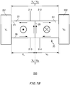
- Figure 7B illustrates the potential difference between respective detection electrodes when the magnetization direction of the first region 21 is the positive direction and the magnetization direction of the second region 22 is the negative direction.
- current in the first region 21 passes through the first drive electrode 201, the second edge 26, the boundary 28, the first edge 25 and the first drive electrode 201 in this order.
- current in the second region 22 passes through the second drive electrode 202, the second edge 26, the boundary 28, the first edge 25 and the second drive electrode 202 in this order.
- the voltage of a portion of the second edge 26 corresponding to the first region 21 is V L , the same voltage as the first drive electrode 201.
- the voltage of a portion of the second edge 26 corresponding to the second region 22 is V R , the same voltage as the second drive electrode 202.
- the voltage of the boundary 28 is (V L + V R )/2, which is the average voltage of the voltage V L of the first drive electrode 201 and the voltage V R of the second drive electrode 202.
- the voltage of the entire first edge 25 is also (V L + V R )/2 in a similar manner to the boundary 28.
- no potential difference is generated between the first detection electrode 211 and the second detection electrode 212, but a potential difference of V L - V R is generated between the third detection electrode 213 and the fourth detection electrode 214. Also, a potential difference of (V R - V L )/2 is generated between the first detection electrode 211 and the third detection electrode 213. Similarly, a potential difference of (V R - V L )/2 is also generated between the second detection electrode 212 and the fourth detection electrode 214. The potential difference between the first detection electrode 211 and the fourth detection electrode 214 and the potential difference between the second detection electrode 212 and the third detection electrode 213 may also be used. It can be determined, from some or all of the information about these potential differences between the detection electrodes, that the magnetization direction of the first region 21 is the positive direction and the magnetization direction of the second region 22 is the negative direction.
- the magnetization direction of the first region 21 is the negative direction and the magnetization direction of the second region 22 is the positive direction, from information about the potential differences between the detection electrodes.
- the voltage of the second edge 26 in the first region 21 is V R while the voltage of the second edge 26 in the second region 22 is V L .
- Other voltages are similar to those in the example of Figure 7B .
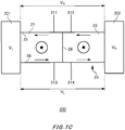
- Figure 7C illustrates the potential difference between respective detection electrodes when the magnetization directions of the first region 21 and the second region 22 are both the positive direction.
- current flows along the first edge 25 from the second drive electrode 202 toward the first drive electrode 201.
- the voltage of the entire first edge 25 is V R , the same voltage as the second drive electrode 202.
- no potential difference is generated between the first detection electrode 211 and the second detection electrode 212.
- no potential difference is generated between the third detection electrode 213 and the fourth detection electrode 214.
- a potential difference of V R - V L is generated between the first detection electrode 211 and the third detection electrode 213.
- the potential difference has the opposite sign of the potential difference in the example of Figure 7A .
- a potential difference of V R - V L is also generated between the second detection electrode 212 and the fourth detection electrode 214.
- the potential difference between the first detection electrode 211 and the fourth detection electrode 214 and the potential difference between the second detection electrode 212 and the third detection electrode 213 may also be used. It can be determined, from some or all of the information about these potential differences between the detection electrodes, that the magnetization directions of the first region 21 and the second region 22 are both the positive direction.
- Figure 8 shows the potential difference between the first detection electrode 211 and the second detection electrode 212 and the potential difference between the third detection electrode 213 and the fourth detection electrode 214 when the external magnetic field is increased and decreased, represented as electrical resistances.
- the potential difference between the first detection electrode 211 and the second detection electrode 212 is indicated by a resistance R T
- the potential difference between the third detection electrode 213 and the fourth detection electrode 214 is indicated by a resistance R B .
- the product of each electrical resistance and the current that flows therethrough is equivalent to the potential difference between detection electrodes. Note that each electrical resistance merely represents a potential difference rather than indicating the actual electrical resistance. No energy dissipation is caused along the first edge 25 and the second edge 26, and therefore the actual power consumption is zero.
- the resistance R T or the resistance R B is non-zero when the magnetization directions of the first region 21 and the second region 22 are different from each other. That is, as described with reference to Figures 4 and 5 , the resistance R B takes non-zero values when the external magnetic field B is larger than or equal to B1 and smaller than B2 in the process of increasing the external magnetic field. Also, the resistance R T takes non-zero values when the external magnetic field B is larger than -B2 and smaller than or equal to -B1 in the process of decreasing the external magnetic field.
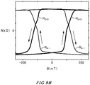
- Figures 9A , 9B and 9C show measurement results of the electrical resistance R when the external magnetic field B applied to the electronic device 200 is varied.
- the substrate 10 is an InP substrate
- the composition of the topological insulator 20 is Cr 0.2 (Bi 0.22 Sb 0.78 ) 1.8 Te 3 .
- the thickness of the topological insulator 20 is set to 8 nm.
- the topological insulator 20 is formed on the substrate 10, and then it is arranged in a vacuum chamber. The degree of vacuum in the vacuum chamber is 3 ⁇ 10 -4 Pa or less.
- a partial region of the surface of the topological insulator 20 in the vacuum chamber is irradiated with argon ions.
- the accelerating voltage of argon ions is 800 V
- the amount of current supplied to an ion gun to generate argon ions is 30 mA
- the irradiation angle of argon ions relative to the surface of the topological insulator 20 is 45 degrees
- the irradiation time with argon ions is 1 second.
- Figure 9A shows a resistance R 1-3 according to the potential difference between the first detection electrode 211 and the third detection electrode 213, and a resistance R 2-4 according to the potential difference between the second detection electrode 212 and the fourth detection electrode 214.
- the waveform of the resistance R 1-3 corresponds to the magnetization curve of the first region 21.
- the waveform of the resistance R 2-4 corresponds to the magnetization curve of the second region 22.
- FIG 9A it can be seen that the coercivity difference between the first region 21 and the second region 22 occurs due to the irradiation with argon ions.
- Figure 9B shows a resistance R 2-3 according to the potential difference between the second detection electrode 212 and the third detection electrode 213, and a resistance R 4-1 according to the potential difference between the fourth detection electrode 214 and the first detection electrode 211. It can also be seen from Figure 9B that the coercivity varies between the first region 21 and the second region 22 due to the irradiation with argon ions.
- Figure 9C shows a resistance R 2-1 according to the potential difference between the second detection electrode 212 and the first detection electrode 211, and a resistance R 4-3 according to the potential difference between the fourth detection electrode 214 and the third detection electrode 213.
- the resistance R 4-3 corresponds to the resistance R B shown in Figure 8
- the resistance R 2-1 corresponds to the resistance R T shown in Figure 8 .
- the coercivity varies between the first region 21 and the second region 22 due to the irradiation with argon ions.
- Figs. 9A-C it can be seen that the magnetization directions of the first region 21 and the second region 22 can be detected based on the respective resistances.
- surplus resistances include, for example, the contact resistance between each electrode and the topological insulator 20, and the like.
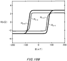
- Figures 10A , 10B and 10C show variation in the coercivity of the second region 22 when the accelerating voltage of argon ions is varied. Note that the irradiation time with argon ions is set to 5 seconds. Other conditions are the same as in the examples of Figures 9A to 9C . Also, in Figures 10A , 10B and 10C , the magnetization curve of the first region 21 is indicated by the resistance R 1-3 , and the magnetization curve of the second region 22 is indicated by the resistance R 2-4 .
- Figure 10A shows the case where the accelerating voltage of argon ions is set to 300 V. In this case, the coercivity of the second region 22 does not significantly vary from the coercivity of the first region 21.
- Figure 10B shows the case where the accelerating voltage of argon ions is set to 400 V. It can be seen that the coercivity of the second region 22 is larger than the coercivity of the first region 21.
- Figure 10C shows the case where the accelerating voltage of argon ions is set to 500 V. It can be seen that the coercivity of the second region 22 is further increased.
- the coercivity of the second region 22 can be controlled according to the accelerating voltage of argon ions. If the difference between the coercivities of the first region 21 and the second region 22 is too small, it is difficult to control the magnetization directions of the first region 21 and the second region 22 independently with an external magnetic field. However, it can be seen that the difference between the coercivities can be made sufficiently large by adjusting the accelerating voltage of argon ions.
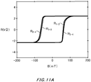
- Figures 11A , 11B and 11C show variation in the coercivity of the second region 22 when the irradiation time with argon ions is varied. Note that the accelerating voltage of argon ions is set to 300 V. Other conditions are the same as in the examples of Figures 9A to 9C .
- Figures 11A shows the case where the irradiation time with argon ions is set to 5 seconds. That is, it is the same condition as in the case of Figure 10A .
- the coercivity of the second region 22 does not significantly vary from the coercivity of the first region 21.
- Figures 11B shows the case where the irradiation time with argon ions is set to 7 seconds. The coercivity of the second region 22 is not significantly changed even though the irradiation time is increased.
- Figures 11C shows the case where the irradiation time with argon ions is set to 9 seconds. It can be seen that the coercivity of the second region 22 is not significantly changed even though the irradiation time is further increased.
- the coercivity of the second region 22 is not significantly changed due to the irradiation time with argon ions.
- the irradiation time with argon ions may be shortened, as long as the coercivity of the second region 22 is changed.
- the irradiation time with argon ions may be 5 seconds or less, or may be 1 second or less.
- Figure 12 is a schematic view showing another example of the surface structure of the electronic device 200.
- the topological insulator 20 in the present example has a first region 21, a second region 22, a third region 23 and a fourth region 24.
- the number of regions may also be three, or may be five or more.
- the plurality of regions are arranged in order between the first drive electrode 201 and the second drive electrode 202.
- Detection electrodes (a first detection electrode 211, a second detection electrode 212, a third detection electrode 213, a fourth detection electrode 214, a fifth detection electrode 215, a sixth detection electrode 216, a seventh detection electrode 217 and an eighth detection electrode 218, in the present example) are connected to the first edge 25 and the second edge of respective regions.
- the plurality of regions may be arranged in order of the magnitude of coercivity between the first drive electrode 201 and the second drive electrode 202.
- the position of the boundary 28 between regions in which the magnetization direction is reversed can be controlled by an external magnetic field.
- information can be stored in the electronic device 200 based on the position of the boundary 28.
- regions having the first coercivity and regions having the second coercivity may be arranged alternately between the first drive electrode 201 and the second drive electrode 202.
- the third region 23 has the same coercivity as the first region 21, and the fourth region 24 has the same coercivity as the second region 22. That is, a plurality of sets of the arrangement of regions shown in Figure 6 are arranged repeatedly.
- the electronic device 200 may average the voltages of detection electrodes connected to the same edge of regions having the same coercivity. For example, the voltages of the first detection electrode 211 and the fifth detection electrode 215 may be averaged for use. With such a configuration, the effect of variability in the contact resistances or the like between the detection electrodes and the topological insulator 20 can be reduced.
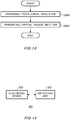
- FIG. 13 is a flowchart showing an example of a fabrication method of the topological insulator 20.
- a topological insulator having magnetism and the first coercivity is prepared (S400).
- a topological insulator having a thin-film shape may be formed on the upper surface of an InP substrate or the like.
- a partial region of the surface of the prepared topological insulator is irradiated with ions of argon or the like (S402).
- argon ions are accelerated with an accelerating voltage of 400 V or more, for example, to irradiate the surface of the topological insulator.
- the ion irradiation damages a partial region of the topological insulator and changes the coercivity.
- the topological insulator 20 having a plurality of regions with magnetism and different coercivities can be fabricated.
- FIG 14 is a block diagram showing an example of a memory device 300.
- the memory device 300 is a device for storing information and includes an electronic device 200 and a detection unit 302.
- the electronic device 200 is any one of the electronic devices 200 described with reference to Figures 1 to 12 .
- the detection unit 302 detects the direction of magnetization of each of the first region 21 and the second region 22 of the topological insulator 20 included in the electronic device 200. As described with reference to Figures 7A to 7C for example, the detection unit 302 may detect the direction of magnetization based on the potential differences between a plurality of pairs of detection electrodes. The direction of magnetization of each region corresponds to one bit of information.
- the detection unit 302 determines that the directions of magnetization of the first region 21 and the second region 22 are both the negative direction.
- the detection unit 302 may use the sign of the potential difference between the first detection electrode 211 and the third detection electrode 213. In this case, the detection unit 302 detects two bits of information "00", for example.
- the detection unit 302 determines that the directions of magnetization of the first region 21 and the second region 22 are both the negative direction.
- the detection unit 302 may use the sign of the potential difference between the first detection electrode 211 and the third detection electrode 213. In this case, the detection unit 302 detects two bits of information "11", for example.
- the detection unit 302 may determine that the direction of magnetization of the first region 21 is the positive direction and the direction of magnetization of second region 22 is the negative direction. In this case, the detection unit 302 detects two bits of information "10", for example.
- the detection unit 302 may determine that the direction of magnetization of the first region 21 is the negative direction and the direction of magnetization of second region 22 is the positive direction. In this case, the detection unit 302 detects two bits of information "01", for example.
- the energy dissipation of current flowing along the edges of the topological insulator 20 is zero, and therefore the power consumption in the memory device 300 when the detection unit 302 reads information can be made very low. Also, even if the storage capacity of the memory device 300 is increased, the increase ratio of power consumption relative to the increase ratio of the storage capacity is very small.
- the memory device 300 may further include a writing unit to write information in the electronic device 200.
- a writing unit to write information in the electronic device 200.
- the magnitude of an external magnetic field to be applied to the topological insulator 20 is preset on the writing unit.
- the magnitude of the external magnetic field can be set based on the magnetization curve of each region of the topological insulator 20.
Landscapes
- Engineering & Computer Science (AREA)
- Computer Hardware Design (AREA)
- Power Engineering (AREA)
- Chemical & Material Sciences (AREA)
- Manufacturing & Machinery (AREA)
- Life Sciences & Earth Sciences (AREA)
- General Health & Medical Sciences (AREA)
- Molecular Biology (AREA)
- Nanotechnology (AREA)
- Biomedical Technology (AREA)
- Health & Medical Sciences (AREA)
- Crystallography & Structural Chemistry (AREA)
- Hall/Mr Elements (AREA)
- Mram Or Spin Memory Techniques (AREA)
- Thin Magnetic Films (AREA)
Applications Claiming Priority (2)
| Application Number | Priority Date | Filing Date | Title |
|---|---|---|---|
| JP2015160198A JP6679095B2 (ja) | 2015-08-14 | 2015-08-14 | 電子デバイス、トポロジカル絶縁体、トポロジカル絶縁体の製造方法およびメモリ装置 |
| PCT/JP2016/072542 WO2017029976A1 (ja) | 2015-08-14 | 2016-08-01 | 電子デバイス、トポロジカル絶縁体、トポロジカル絶縁体の製造方法およびメモリ装置 |
Publications (3)
| Publication Number | Publication Date |
|---|---|
| EP3336902A1 true EP3336902A1 (de) | 2018-06-20 |
| EP3336902A4 EP3336902A4 (de) | 2018-08-22 |
| EP3336902B1 EP3336902B1 (de) | 2019-06-26 |
Family
ID=58047868
Family Applications (1)
| Application Number | Title | Priority Date | Filing Date |
|---|---|---|---|
| EP16836967.6A Active EP3336902B1 (de) | 2015-08-14 | 2016-08-01 | Elektronische vorrichtung, topologischer isolator, verfahren zur herstellung eines topologischen isolators und speichervorrichtung |
Country Status (4)
| Country | Link |
|---|---|
| US (1) | US10468586B2 (de) |
| EP (1) | EP3336902B1 (de) |
| JP (1) | JP6679095B2 (de) |
| WO (1) | WO2017029976A1 (de) |
Families Citing this family (2)
| Publication number | Priority date | Publication date | Assignee | Title |
|---|---|---|---|---|
| US10283611B2 (en) * | 2016-09-27 | 2019-05-07 | Industry-Academic Cooperation Foundation, Yonsei University | Electronic device including topological insulator and transition metal oxide |
| EP4187626A1 (de) | 2021-11-25 | 2023-05-31 | Imec VZW | Thermisch stabile spin-bahn-drehmoment (sot) schicht für eine mram-vorrichtung |
Family Cites Families (14)
| Publication number | Priority date | Publication date | Assignee | Title |
|---|---|---|---|---|
| US3956769A (en) * | 1974-08-12 | 1976-05-11 | Control Data Corporation | Recording system having coinciding servo and data tracks |
| KR20050084904A (ko) * | 2002-11-01 | 2005-08-29 | 코닌클리케 필립스 일렉트로닉스 엔.브이. | 자구확장 롬 매체용 처리방식 |
| EP1705665B1 (de) * | 2005-03-24 | 2008-04-02 | Hitachi Ltd. | Leitungssteuerungsanordnung |
| WO2009133744A1 (ja) * | 2008-04-28 | 2009-11-05 | 日本電気株式会社 | 磁気記憶素子、及び磁気メモリ |
| KR20110044046A (ko) * | 2009-10-22 | 2011-04-28 | 주식회사 하이닉스반도체 | 균일한 토폴로지를 갖는 반도체 소자 제조 방법 |
| US8279662B2 (en) | 2010-11-11 | 2012-10-02 | Seagate Technology Llc | Multi-bit magnetic memory with independently programmable free layer domains |
| US20120138115A1 (en) * | 2010-12-06 | 2012-06-07 | Purdue Research Foundation | Surface excitonic thermoelectric devices |
| WO2013172815A1 (en) * | 2012-05-14 | 2013-11-21 | The Johns Hopkins University | Simplified devices utilizing novel pn-semiconductor structures |
| EP2741295B1 (de) | 2012-12-04 | 2016-03-02 | Imec | Magnetische STT-Speichervorrichtung |
| CN102995117B (zh) * | 2012-12-21 | 2015-06-10 | 清华大学 | 拓扑绝缘体结构的制备方法 |
| KR101894828B1 (ko) * | 2013-11-15 | 2018-09-04 | 내셔날 인스티튜트 오브 어드밴스드 인더스트리얼 사이언스 앤드 테크놀로지 | 정보 기록 장치, 정보 기록 방법 및 정보 재생 방법 |
| KR102176582B1 (ko) * | 2013-11-19 | 2020-11-09 | 삼성전자주식회사 | 위상 절연체를 이용한 표면 플라즈몬 및 편광 검출소자와 그 제조방법 및 표면 플라즈몬과 편광 검출방법 |
| US10132880B2 (en) * | 2014-12-10 | 2018-11-20 | The United States of America, as represented by the Secratary of the Navy | Direct electrical detection of current-induced spin polarization due to spin-momentum locking in topological insulators |
| US9806710B2 (en) * | 2016-03-31 | 2017-10-31 | University Of Iowa Research Foundation | Voltage-controlled magnetic-based devices having topological insulator/magnetic insulator heterostructure |
-
2015
- 2015-08-14 JP JP2015160198A patent/JP6679095B2/ja active Active
-
2016
- 2016-08-01 WO PCT/JP2016/072542 patent/WO2017029976A1/ja not_active Ceased
- 2016-08-01 EP EP16836967.6A patent/EP3336902B1/de active Active
-
2018
- 2018-02-12 US US15/894,904 patent/US10468586B2/en active Active
Also Published As
| Publication number | Publication date |
|---|---|
| WO2017029976A1 (ja) | 2017-02-23 |
| EP3336902B1 (de) | 2019-06-26 |
| JP2017038032A (ja) | 2017-02-16 |
| EP3336902A4 (de) | 2018-08-22 |
| US20180175285A1 (en) | 2018-06-21 |
| US10468586B2 (en) | 2019-11-05 |
| JP6679095B2 (ja) | 2020-04-15 |
Similar Documents
| Publication | Publication Date | Title |
|---|---|---|
| del Valle et al. | Electrically induced multiple metal-insulator transitions in oxide nanodevices | |
| US10141037B2 (en) | Magnetic memory device | |
| KR101998268B1 (ko) | 반도체 소자 | |
| US10395709B2 (en) | Magnetic memory device | |
| JP4533837B2 (ja) | 電圧制御磁化反転記録方式のmram素子及びそれを利用した情報の記録及び読み出し方法 | |
| KR102582983B1 (ko) | 자성 메모리 소자 | |
| EP1708257A1 (de) | Strominjektions-magnetdomänen-wandbewegungselement | |
| US6727537B2 (en) | Magnetic memory cell | |
| CN114038993B (zh) | 一种磁性异质结结构及调控实现逻辑与多态存储功能的方法 | |
| US10468586B2 (en) | Electronic device, topological insulator, fabrication method of topological insulator and memory device | |
| CN109891613B (zh) | 半导体器件和半导体逻辑器件 | |
| KR101829452B1 (ko) | 자기 메모리 소자 | |
| US20220350572A1 (en) | Random number generation unit and computing system | |
| Aronzon et al. | Conductivity, magnetoresistance, and the Hall effect in granular Fe/SiO2 films | |
| Fritz et al. | Ultralow Switching-Current Density in All-Amorphous W-Hf/Co-Fe-B/Ta O x Films | |
| Fukumoto et al. | High thermal stability of magnetic tunnel junctions with oxide diffusion barrier layers | |
| WO2020256776A1 (en) | Perpendicular sot mram | |
| US7466585B2 (en) | Magnetic random access memory | |
| CN102768854A (zh) | 一种磁电复合多态存储器单元及其制备方法 | |
| US10998490B2 (en) | Magnetic element | |
| KR102024876B1 (ko) | Sot 반도체 소자 및 sot 반도체 소자의 기록 방법 | |
| Larson | Atom probe characterization of nanomagnetic materials | |
| Feng et al. | Observation of Dzyaloshinskii-Moriya interaction and efficient perpendicular magnetization switching in sputtered (BiSb) 2 Te 3-ferromagnet heterostructures | |
| KR101474665B1 (ko) | 스핀 전달 토크 자기터널접합 소자, 그 동작 방법 및 그를 채용하는 자기저항 메모리 소자 | |
| Shirokura et al. | Origin of the giant spin Hall effect in BiSb topological insulator |
Legal Events
| Date | Code | Title | Description |
|---|---|---|---|
| STAA | Information on the status of an ep patent application or granted ep patent |
Free format text: STATUS: THE INTERNATIONAL PUBLICATION HAS BEEN MADE |
|
| PUAI | Public reference made under article 153(3) epc to a published international application that has entered the european phase |
Free format text: ORIGINAL CODE: 0009012 |
|
| STAA | Information on the status of an ep patent application or granted ep patent |
Free format text: STATUS: REQUEST FOR EXAMINATION WAS MADE |
|
| 17P | Request for examination filed |
Effective date: 20180209 |
|
| AK | Designated contracting states |
Kind code of ref document: A1 Designated state(s): AL AT BE BG CH CY CZ DE DK EE ES FI FR GB GR HR HU IE IS IT LI LT LU LV MC MK MT NL NO PL PT RO RS SE SI SK SM TR |
|
| AX | Request for extension of the european patent |
Extension state: BA ME |
|
| REG | Reference to a national code |
Ref country code: DE Ref legal event code: R079 Ref document number: 602016016074 Country of ref document: DE Free format text: PREVIOUS MAIN CLASS: H01L0029820000 Ipc: H01F0001000000 |
|
| A4 | Supplementary search report drawn up and despatched |
Effective date: 20180719 |
|
| RIC1 | Information provided on ipc code assigned before grant |
Ipc: H01L 43/12 20060101ALI20180713BHEP Ipc: H01F 10/26 20060101ALI20180713BHEP Ipc: H01L 43/10 20060101ALI20180713BHEP Ipc: G11C 11/155 20060101ALI20180713BHEP Ipc: H01F 1/00 20060101AFI20180713BHEP Ipc: H01L 43/08 20060101ALI20180713BHEP |
|
| DAV | Request for validation of the european patent (deleted) | ||
| DAX | Request for extension of the european patent (deleted) | ||
| GRAP | Despatch of communication of intention to grant a patent |
Free format text: ORIGINAL CODE: EPIDOSNIGR1 |
|
| STAA | Information on the status of an ep patent application or granted ep patent |
Free format text: STATUS: GRANT OF PATENT IS INTENDED |
|
| INTG | Intention to grant announced |
Effective date: 20190212 |
|
| GRAS | Grant fee paid |
Free format text: ORIGINAL CODE: EPIDOSNIGR3 |
|
| GRAA | (expected) grant |
Free format text: ORIGINAL CODE: 0009210 |
|
| STAA | Information on the status of an ep patent application or granted ep patent |
Free format text: STATUS: THE PATENT HAS BEEN GRANTED |
|
| AK | Designated contracting states |
Kind code of ref document: B1 Designated state(s): AL AT BE BG CH CY CZ DE DK EE ES FI FR GB GR HR HU IE IS IT LI LT LU LV MC MK MT NL NO PL PT RO RS SE SI SK SM TR |
|
| REG | Reference to a national code |
Ref country code: GB Ref legal event code: FG4D |
|
| REG | Reference to a national code |
Ref country code: CH Ref legal event code: EP |
|
| REG | Reference to a national code |
Ref country code: AT Ref legal event code: REF Ref document number: 1149256 Country of ref document: AT Kind code of ref document: T Effective date: 20190715 |
|
| REG | Reference to a national code |
Ref country code: DE Ref legal event code: R096 Ref document number: 602016016074 Country of ref document: DE |
|
| REG | Reference to a national code |
Ref country code: IE Ref legal event code: FG4D |
|
| REG | Reference to a national code |
Ref country code: NL Ref legal event code: MP Effective date: 20190626 |
|
| PG25 | Lapsed in a contracting state [announced via postgrant information from national office to epo] |
Ref country code: FI Free format text: LAPSE BECAUSE OF FAILURE TO SUBMIT A TRANSLATION OF THE DESCRIPTION OR TO PAY THE FEE WITHIN THE PRESCRIBED TIME-LIMIT Effective date: 20190626 Ref country code: NO Free format text: LAPSE BECAUSE OF FAILURE TO SUBMIT A TRANSLATION OF THE DESCRIPTION OR TO PAY THE FEE WITHIN THE PRESCRIBED TIME-LIMIT Effective date: 20190926 Ref country code: AL Free format text: LAPSE BECAUSE OF FAILURE TO SUBMIT A TRANSLATION OF THE DESCRIPTION OR TO PAY THE FEE WITHIN THE PRESCRIBED TIME-LIMIT Effective date: 20190626 Ref country code: SE Free format text: LAPSE BECAUSE OF FAILURE TO SUBMIT A TRANSLATION OF THE DESCRIPTION OR TO PAY THE FEE WITHIN THE PRESCRIBED TIME-LIMIT Effective date: 20190626 Ref country code: LT Free format text: LAPSE BECAUSE OF FAILURE TO SUBMIT A TRANSLATION OF THE DESCRIPTION OR TO PAY THE FEE WITHIN THE PRESCRIBED TIME-LIMIT Effective date: 20190626 Ref country code: HR Free format text: LAPSE BECAUSE OF FAILURE TO SUBMIT A TRANSLATION OF THE DESCRIPTION OR TO PAY THE FEE WITHIN THE PRESCRIBED TIME-LIMIT Effective date: 20190626 |
|
| REG | Reference to a national code |
Ref country code: LT Ref legal event code: MG4D |
|
| PG25 | Lapsed in a contracting state [announced via postgrant information from national office to epo] |
Ref country code: RS Free format text: LAPSE BECAUSE OF FAILURE TO SUBMIT A TRANSLATION OF THE DESCRIPTION OR TO PAY THE FEE WITHIN THE PRESCRIBED TIME-LIMIT Effective date: 20190626 Ref country code: BG Free format text: LAPSE BECAUSE OF FAILURE TO SUBMIT A TRANSLATION OF THE DESCRIPTION OR TO PAY THE FEE WITHIN THE PRESCRIBED TIME-LIMIT Effective date: 20190926 Ref country code: GR Free format text: LAPSE BECAUSE OF FAILURE TO SUBMIT A TRANSLATION OF THE DESCRIPTION OR TO PAY THE FEE WITHIN THE PRESCRIBED TIME-LIMIT Effective date: 20190927 Ref country code: LV Free format text: LAPSE BECAUSE OF FAILURE TO SUBMIT A TRANSLATION OF THE DESCRIPTION OR TO PAY THE FEE WITHIN THE PRESCRIBED TIME-LIMIT Effective date: 20190626 |
|
| REG | Reference to a national code |
Ref country code: AT Ref legal event code: MK05 Ref document number: 1149256 Country of ref document: AT Kind code of ref document: T Effective date: 20190626 |
|
| PG25 | Lapsed in a contracting state [announced via postgrant information from national office to epo] |
Ref country code: RO Free format text: LAPSE BECAUSE OF FAILURE TO SUBMIT A TRANSLATION OF THE DESCRIPTION OR TO PAY THE FEE WITHIN THE PRESCRIBED TIME-LIMIT Effective date: 20190626 Ref country code: SK Free format text: LAPSE BECAUSE OF FAILURE TO SUBMIT A TRANSLATION OF THE DESCRIPTION OR TO PAY THE FEE WITHIN THE PRESCRIBED TIME-LIMIT Effective date: 20190626 Ref country code: CZ Free format text: LAPSE BECAUSE OF FAILURE TO SUBMIT A TRANSLATION OF THE DESCRIPTION OR TO PAY THE FEE WITHIN THE PRESCRIBED TIME-LIMIT Effective date: 20190626 Ref country code: AT Free format text: LAPSE BECAUSE OF FAILURE TO SUBMIT A TRANSLATION OF THE DESCRIPTION OR TO PAY THE FEE WITHIN THE PRESCRIBED TIME-LIMIT Effective date: 20190626 Ref country code: EE Free format text: LAPSE BECAUSE OF FAILURE TO SUBMIT A TRANSLATION OF THE DESCRIPTION OR TO PAY THE FEE WITHIN THE PRESCRIBED TIME-LIMIT Effective date: 20190626 Ref country code: NL Free format text: LAPSE BECAUSE OF FAILURE TO SUBMIT A TRANSLATION OF THE DESCRIPTION OR TO PAY THE FEE WITHIN THE PRESCRIBED TIME-LIMIT Effective date: 20190626 Ref country code: PT Free format text: LAPSE BECAUSE OF FAILURE TO SUBMIT A TRANSLATION OF THE DESCRIPTION OR TO PAY THE FEE WITHIN THE PRESCRIBED TIME-LIMIT Effective date: 20191028 |
|
| PG25 | Lapsed in a contracting state [announced via postgrant information from national office to epo] |
Ref country code: IT Free format text: LAPSE BECAUSE OF FAILURE TO SUBMIT A TRANSLATION OF THE DESCRIPTION OR TO PAY THE FEE WITHIN THE PRESCRIBED TIME-LIMIT Effective date: 20190626 Ref country code: SM Free format text: LAPSE BECAUSE OF FAILURE TO SUBMIT A TRANSLATION OF THE DESCRIPTION OR TO PAY THE FEE WITHIN THE PRESCRIBED TIME-LIMIT Effective date: 20190626 Ref country code: IS Free format text: LAPSE BECAUSE OF FAILURE TO SUBMIT A TRANSLATION OF THE DESCRIPTION OR TO PAY THE FEE WITHIN THE PRESCRIBED TIME-LIMIT Effective date: 20191026 Ref country code: ES Free format text: LAPSE BECAUSE OF FAILURE TO SUBMIT A TRANSLATION OF THE DESCRIPTION OR TO PAY THE FEE WITHIN THE PRESCRIBED TIME-LIMIT Effective date: 20190626 |
|
| PG25 | Lapsed in a contracting state [announced via postgrant information from national office to epo] |
Ref country code: TR Free format text: LAPSE BECAUSE OF FAILURE TO SUBMIT A TRANSLATION OF THE DESCRIPTION OR TO PAY THE FEE WITHIN THE PRESCRIBED TIME-LIMIT Effective date: 20190626 |
|
| PG25 | Lapsed in a contracting state [announced via postgrant information from national office to epo] |
Ref country code: PL Free format text: LAPSE BECAUSE OF FAILURE TO SUBMIT A TRANSLATION OF THE DESCRIPTION OR TO PAY THE FEE WITHIN THE PRESCRIBED TIME-LIMIT Effective date: 20190626 Ref country code: DK Free format text: LAPSE BECAUSE OF FAILURE TO SUBMIT A TRANSLATION OF THE DESCRIPTION OR TO PAY THE FEE WITHIN THE PRESCRIBED TIME-LIMIT Effective date: 20190626 |
|
| PG25 | Lapsed in a contracting state [announced via postgrant information from national office to epo] |
Ref country code: IS Free format text: LAPSE BECAUSE OF FAILURE TO SUBMIT A TRANSLATION OF THE DESCRIPTION OR TO PAY THE FEE WITHIN THE PRESCRIBED TIME-LIMIT Effective date: 20200320 Ref country code: CH Free format text: LAPSE BECAUSE OF NON-PAYMENT OF DUE FEES Effective date: 20190831 Ref country code: LU Free format text: LAPSE BECAUSE OF NON-PAYMENT OF DUE FEES Effective date: 20190801 Ref country code: LI Free format text: LAPSE BECAUSE OF NON-PAYMENT OF DUE FEES Effective date: 20190831 Ref country code: MC Free format text: LAPSE BECAUSE OF FAILURE TO SUBMIT A TRANSLATION OF THE DESCRIPTION OR TO PAY THE FEE WITHIN THE PRESCRIBED TIME-LIMIT Effective date: 20190626 |
|
| REG | Reference to a national code |
Ref country code: BE Ref legal event code: MM Effective date: 20190831 |
|
| REG | Reference to a national code |
Ref country code: DE Ref legal event code: R097 Ref document number: 602016016074 Country of ref document: DE |
|
| PLBE | No opposition filed within time limit |
Free format text: ORIGINAL CODE: 0009261 |
|
| STAA | Information on the status of an ep patent application or granted ep patent |
Free format text: STATUS: NO OPPOSITION FILED WITHIN TIME LIMIT |
|
| PG2D | Information on lapse in contracting state deleted |
Ref country code: IS |
|
| PG25 | Lapsed in a contracting state [announced via postgrant information from national office to epo] |
Ref country code: IE Free format text: LAPSE BECAUSE OF NON-PAYMENT OF DUE FEES Effective date: 20190801 |
|
| 26N | No opposition filed |
Effective date: 20200603 |
|
| PG25 | Lapsed in a contracting state [announced via postgrant information from national office to epo] |
Ref country code: SI Free format text: LAPSE BECAUSE OF FAILURE TO SUBMIT A TRANSLATION OF THE DESCRIPTION OR TO PAY THE FEE WITHIN THE PRESCRIBED TIME-LIMIT Effective date: 20190626 Ref country code: BE Free format text: LAPSE BECAUSE OF NON-PAYMENT OF DUE FEES Effective date: 20190831 |
|
| GBPC | Gb: european patent ceased through non-payment of renewal fee |
Effective date: 20200801 |
|
| PG25 | Lapsed in a contracting state [announced via postgrant information from national office to epo] |
Ref country code: CY Free format text: LAPSE BECAUSE OF FAILURE TO SUBMIT A TRANSLATION OF THE DESCRIPTION OR TO PAY THE FEE WITHIN THE PRESCRIBED TIME-LIMIT Effective date: 20190626 |
|
| PG25 | Lapsed in a contracting state [announced via postgrant information from national office to epo] |
Ref country code: HU Free format text: LAPSE BECAUSE OF FAILURE TO SUBMIT A TRANSLATION OF THE DESCRIPTION OR TO PAY THE FEE WITHIN THE PRESCRIBED TIME-LIMIT; INVALID AB INITIO Effective date: 20160801 Ref country code: MT Free format text: LAPSE BECAUSE OF FAILURE TO SUBMIT A TRANSLATION OF THE DESCRIPTION OR TO PAY THE FEE WITHIN THE PRESCRIBED TIME-LIMIT Effective date: 20190626 |
|
| PG25 | Lapsed in a contracting state [announced via postgrant information from national office to epo] |
Ref country code: GB Free format text: LAPSE BECAUSE OF NON-PAYMENT OF DUE FEES Effective date: 20200801 |
|
| PG25 | Lapsed in a contracting state [announced via postgrant information from national office to epo] |
Ref country code: MK Free format text: LAPSE BECAUSE OF FAILURE TO SUBMIT A TRANSLATION OF THE DESCRIPTION OR TO PAY THE FEE WITHIN THE PRESCRIBED TIME-LIMIT Effective date: 20190626 |
|
| PGFP | Annual fee paid to national office [announced via postgrant information from national office to epo] |
Ref country code: DE Payment date: 20250820 Year of fee payment: 10 |
|
| PGFP | Annual fee paid to national office [announced via postgrant information from national office to epo] |
Ref country code: FR Payment date: 20250828 Year of fee payment: 10 |