EP3333888A1 - Semiconductor device and fabrication method thereof - Google Patents
Semiconductor device and fabrication method thereof Download PDFInfo
- Publication number
- EP3333888A1 EP3333888A1 EP17205927.1A EP17205927A EP3333888A1 EP 3333888 A1 EP3333888 A1 EP 3333888A1 EP 17205927 A EP17205927 A EP 17205927A EP 3333888 A1 EP3333888 A1 EP 3333888A1
- Authority
- EP
- European Patent Office
- Prior art keywords
- gate electrode
- region
- forming
- base substrate
- step portion
- Prior art date
- Legal status (The legal status is an assumption and is not a legal conclusion. Google has not performed a legal analysis and makes no representation as to the accuracy of the status listed.)
- Withdrawn
Links
Images



Classifications
-
- C—CHEMISTRY; METALLURGY
- C23—COATING METALLIC MATERIAL; COATING MATERIAL WITH METALLIC MATERIAL; CHEMICAL SURFACE TREATMENT; DIFFUSION TREATMENT OF METALLIC MATERIAL; COATING BY VACUUM EVAPORATION, BY SPUTTERING, BY ION IMPLANTATION OR BY CHEMICAL VAPOUR DEPOSITION, IN GENERAL; INHIBITING CORROSION OF METALLIC MATERIAL OR INCRUSTATION IN GENERAL
- C23F—NON-MECHANICAL REMOVAL OF METALLIC MATERIAL FROM SURFACE; INHIBITING CORROSION OF METALLIC MATERIAL OR INCRUSTATION IN GENERAL; MULTI-STEP PROCESSES FOR SURFACE TREATMENT OF METALLIC MATERIAL INVOLVING AT LEAST ONE PROCESS PROVIDED FOR IN CLASS C23 AND AT LEAST ONE PROCESS COVERED BY SUBCLASS C21D OR C22F OR CLASS C25
- C23F1/00—Etching metallic material by chemical means
-
- H—ELECTRICITY
- H10—SEMICONDUCTOR DEVICES; ELECTRIC SOLID-STATE DEVICES NOT OTHERWISE PROVIDED FOR
- H10D—INORGANIC ELECTRIC SEMICONDUCTOR DEVICES
- H10D62/00—Semiconductor bodies, or regions thereof, of devices having potential barriers
- H10D62/10—Shapes, relative sizes or dispositions of the regions of the semiconductor bodies; Shapes of the semiconductor bodies
- H10D62/13—Semiconductor regions connected to electrodes carrying current to be rectified, amplified or switched, e.g. source or drain regions
- H10D62/149—Source or drain regions of field-effect devices
- H10D62/151—Source or drain regions of field-effect devices of IGFETs
-
- H—ELECTRICITY
- H10—SEMICONDUCTOR DEVICES; ELECTRIC SOLID-STATE DEVICES NOT OTHERWISE PROVIDED FOR
- H10D—INORGANIC ELECTRIC SEMICONDUCTOR DEVICES
- H10D64/00—Electrodes of devices having potential barriers
- H10D64/01—Manufacture or treatment
- H10D64/013—Manufacture or treatment of electrodes having a conductor capacitively coupled to a semiconductor by an insulator
- H10D64/01302—Manufacture or treatment of electrodes having a conductor capacitively coupled to a semiconductor by an insulator the insulator being formed after the semiconductor body, the semiconductor being silicon
- H10D64/01304—Manufacture or treatment of electrodes having a conductor capacitively coupled to a semiconductor by an insulator the insulator being formed after the semiconductor body, the semiconductor being silicon characterised by the conductor
- H10D64/01324—Manufacture or treatment of electrodes having a conductor capacitively coupled to a semiconductor by an insulator the insulator being formed after the semiconductor body, the semiconductor being silicon characterised by the conductor characterised by the sectional shape, e.g. T or inverted-T
-
- H—ELECTRICITY
- H10—SEMICONDUCTOR DEVICES; ELECTRIC SOLID-STATE DEVICES NOT OTHERWISE PROVIDED FOR
- H10D—INORGANIC ELECTRIC SEMICONDUCTOR DEVICES
- H10D64/00—Electrodes of devices having potential barriers
- H10D64/20—Electrodes characterised by their shapes, relative sizes or dispositions
- H10D64/27—Electrodes not carrying the current to be rectified, amplified, oscillated or switched, e.g. gates
- H10D64/311—Gate electrodes for field-effect devices
- H10D64/411—Gate electrodes for field-effect devices for FETs
- H10D64/511—Gate electrodes for field-effect devices for FETs for IGFETs
- H10D64/517—Gate electrodes for field-effect devices for FETs for IGFETs characterised by the conducting layers
- H10D64/518—Gate electrodes for field-effect devices for FETs for IGFETs characterised by the conducting layers characterised by their lengths or sectional shapes
-
- H—ELECTRICITY
- H10—SEMICONDUCTOR DEVICES; ELECTRIC SOLID-STATE DEVICES NOT OTHERWISE PROVIDED FOR
- H10D—INORGANIC ELECTRIC SEMICONDUCTOR DEVICES
- H10D84/00—Integrated devices formed in or on semiconductor substrates that comprise only semiconducting layers, e.g. on Si wafers or on GaAs-on-Si wafers
- H10D84/01—Manufacture or treatment
- H10D84/0123—Integrating together multiple components covered by H10D12/00 or H10D30/00, e.g. integrating multiple IGBTs
- H10D84/0126—Integrating together multiple components covered by H10D12/00 or H10D30/00, e.g. integrating multiple IGBTs the components including insulated gates, e.g. IGFETs
- H10D84/013—Manufacturing their source or drain regions, e.g. silicided source or drain regions
-
- H—ELECTRICITY
- H10—SEMICONDUCTOR DEVICES; ELECTRIC SOLID-STATE DEVICES NOT OTHERWISE PROVIDED FOR
- H10D—INORGANIC ELECTRIC SEMICONDUCTOR DEVICES
- H10D84/00—Integrated devices formed in or on semiconductor substrates that comprise only semiconducting layers, e.g. on Si wafers or on GaAs-on-Si wafers
- H10D84/01—Manufacture or treatment
- H10D84/0123—Integrating together multiple components covered by H10D12/00 or H10D30/00, e.g. integrating multiple IGBTs
- H10D84/0126—Integrating together multiple components covered by H10D12/00 or H10D30/00, e.g. integrating multiple IGBTs the components including insulated gates, e.g. IGFETs
- H10D84/0135—Manufacturing their gate conductors
- H10D84/0142—Manufacturing their gate conductors the gate conductors having different shapes or dimensions
-
- H—ELECTRICITY
- H10—SEMICONDUCTOR DEVICES; ELECTRIC SOLID-STATE DEVICES NOT OTHERWISE PROVIDED FOR
- H10D—INORGANIC ELECTRIC SEMICONDUCTOR DEVICES
- H10D84/00—Integrated devices formed in or on semiconductor substrates that comprise only semiconducting layers, e.g. on Si wafers or on GaAs-on-Si wafers
- H10D84/01—Manufacture or treatment
- H10D84/02—Manufacture or treatment characterised by using material-based technologies
- H10D84/03—Manufacture or treatment characterised by using material-based technologies using Group IV technology, e.g. silicon technology or silicon-carbide [SiC] technology
- H10D84/038—Manufacture or treatment characterised by using material-based technologies using Group IV technology, e.g. silicon technology or silicon-carbide [SiC] technology using silicon technology, e.g. SiGe
-
- H—ELECTRICITY
- H10—SEMICONDUCTOR DEVICES; ELECTRIC SOLID-STATE DEVICES NOT OTHERWISE PROVIDED FOR
- H10D—INORGANIC ELECTRIC SEMICONDUCTOR DEVICES
- H10D84/00—Integrated devices formed in or on semiconductor substrates that comprise only semiconducting layers, e.g. on Si wafers or on GaAs-on-Si wafers
- H10D84/80—Integrated devices formed in or on semiconductor substrates that comprise only semiconducting layers, e.g. on Si wafers or on GaAs-on-Si wafers characterised by the integration of at least one component covered by groups H10D12/00 or H10D30/00, e.g. integration of IGFETs
- H10D84/82—Integrated devices formed in or on semiconductor substrates that comprise only semiconducting layers, e.g. on Si wafers or on GaAs-on-Si wafers characterised by the integration of at least one component covered by groups H10D12/00 or H10D30/00, e.g. integration of IGFETs of only field-effect components
- H10D84/83—Integrated devices formed in or on semiconductor substrates that comprise only semiconducting layers, e.g. on Si wafers or on GaAs-on-Si wafers characterised by the integration of at least one component covered by groups H10D12/00 or H10D30/00, e.g. integration of IGFETs of only field-effect components of only insulated-gate FETs [IGFET]
-
- H—ELECTRICITY
- H10—SEMICONDUCTOR DEVICES; ELECTRIC SOLID-STATE DEVICES NOT OTHERWISE PROVIDED FOR
- H10D—INORGANIC ELECTRIC SEMICONDUCTOR DEVICES
- H10D84/00—Integrated devices formed in or on semiconductor substrates that comprise only semiconducting layers, e.g. on Si wafers or on GaAs-on-Si wafers
- H10D84/80—Integrated devices formed in or on semiconductor substrates that comprise only semiconducting layers, e.g. on Si wafers or on GaAs-on-Si wafers characterised by the integration of at least one component covered by groups H10D12/00 or H10D30/00, e.g. integration of IGFETs
- H10D84/82—Integrated devices formed in or on semiconductor substrates that comprise only semiconducting layers, e.g. on Si wafers or on GaAs-on-Si wafers characterised by the integration of at least one component covered by groups H10D12/00 or H10D30/00, e.g. integration of IGFETs of only field-effect components
- H10D84/83—Integrated devices formed in or on semiconductor substrates that comprise only semiconducting layers, e.g. on Si wafers or on GaAs-on-Si wafers characterised by the integration of at least one component covered by groups H10D12/00 or H10D30/00, e.g. integration of IGFETs of only field-effect components of only insulated-gate FETs [IGFET]
- H10D84/834—Integrated devices formed in or on semiconductor substrates that comprise only semiconducting layers, e.g. on Si wafers or on GaAs-on-Si wafers characterised by the integration of at least one component covered by groups H10D12/00 or H10D30/00, e.g. integration of IGFETs of only field-effect components of only insulated-gate FETs [IGFET] comprising FinFETs
-
- H—ELECTRICITY
- H10—SEMICONDUCTOR DEVICES; ELECTRIC SOLID-STATE DEVICES NOT OTHERWISE PROVIDED FOR
- H10P—GENERIC PROCESSES OR APPARATUS FOR THE MANUFACTURE OR TREATMENT OF DEVICES COVERED BY CLASS H10
- H10P50/00—Etching of wafers, substrates or parts of devices
- H10P50/20—Dry etching; Plasma etching; Reactive-ion etching
- H10P50/26—Dry etching; Plasma etching; Reactive-ion etching of conductive or resistive materials
- H10P50/264—Dry etching; Plasma etching; Reactive-ion etching of conductive or resistive materials by chemical means
- H10P50/266—Dry etching; Plasma etching; Reactive-ion etching of conductive or resistive materials by chemical means by vapour etching only
-
- H—ELECTRICITY
- H10—SEMICONDUCTOR DEVICES; ELECTRIC SOLID-STATE DEVICES NOT OTHERWISE PROVIDED FOR
- H10P—GENERIC PROCESSES OR APPARATUS FOR THE MANUFACTURE OR TREATMENT OF DEVICES COVERED BY CLASS H10
- H10P50/00—Etching of wafers, substrates or parts of devices
- H10P50/20—Dry etching; Plasma etching; Reactive-ion etching
- H10P50/26—Dry etching; Plasma etching; Reactive-ion etching of conductive or resistive materials
- H10P50/264—Dry etching; Plasma etching; Reactive-ion etching of conductive or resistive materials by chemical means
- H10P50/266—Dry etching; Plasma etching; Reactive-ion etching of conductive or resistive materials by chemical means by vapour etching only
- H10P50/267—Dry etching; Plasma etching; Reactive-ion etching of conductive or resistive materials by chemical means by vapour etching only using plasmas
- H10P50/268—Dry etching; Plasma etching; Reactive-ion etching of conductive or resistive materials by chemical means by vapour etching only using plasmas of silicon-containing layers
-
- H—ELECTRICITY
- H10—SEMICONDUCTOR DEVICES; ELECTRIC SOLID-STATE DEVICES NOT OTHERWISE PROVIDED FOR
- H10P—GENERIC PROCESSES OR APPARATUS FOR THE MANUFACTURE OR TREATMENT OF DEVICES COVERED BY CLASS H10
- H10P50/00—Etching of wafers, substrates or parts of devices
- H10P50/71—Etching of wafers, substrates or parts of devices using masks for conductive or resistive materials
-
- H—ELECTRICITY
- H10—SEMICONDUCTOR DEVICES; ELECTRIC SOLID-STATE DEVICES NOT OTHERWISE PROVIDED FOR
- H10D—INORGANIC ELECTRIC SEMICONDUCTOR DEVICES
- H10D30/00—Field-effect transistors [FET]
- H10D30/60—Insulated-gate field-effect transistors [IGFET]
- H10D30/791—Arrangements for exerting mechanical stress on the crystal lattice of the channel regions
- H10D30/797—Arrangements for exerting mechanical stress on the crystal lattice of the channel regions being in source or drain regions, e.g. SiGe source or drain
-
- H—ELECTRICITY
- H10—SEMICONDUCTOR DEVICES; ELECTRIC SOLID-STATE DEVICES NOT OTHERWISE PROVIDED FOR
- H10D—INORGANIC ELECTRIC SEMICONDUCTOR DEVICES
- H10D62/00—Semiconductor bodies, or regions thereof, of devices having potential barriers
- H10D62/80—Semiconductor bodies, or regions thereof, of devices having potential barriers characterised by the materials
- H10D62/83—Semiconductor bodies, or regions thereof, of devices having potential barriers characterised by the materials being Group IV materials, e.g. B-doped Si or undoped Ge
- H10D62/832—Semiconductor bodies, or regions thereof, of devices having potential barriers characterised by the materials being Group IV materials, e.g. B-doped Si or undoped Ge being Group IV materials comprising two or more elements, e.g. SiGe
-
- H—ELECTRICITY
- H10—SEMICONDUCTOR DEVICES; ELECTRIC SOLID-STATE DEVICES NOT OTHERWISE PROVIDED FOR
- H10D—INORGANIC ELECTRIC SEMICONDUCTOR DEVICES
- H10D62/00—Semiconductor bodies, or regions thereof, of devices having potential barriers
- H10D62/80—Semiconductor bodies, or regions thereof, of devices having potential barriers characterised by the materials
- H10D62/83—Semiconductor bodies, or regions thereof, of devices having potential barriers characterised by the materials being Group IV materials, e.g. B-doped Si or undoped Ge
- H10D62/832—Semiconductor bodies, or regions thereof, of devices having potential barriers characterised by the materials being Group IV materials, e.g. B-doped Si or undoped Ge being Group IV materials comprising two or more elements, e.g. SiGe
- H10D62/8325—Silicon carbide
-
- H—ELECTRICITY
- H10—SEMICONDUCTOR DEVICES; ELECTRIC SOLID-STATE DEVICES NOT OTHERWISE PROVIDED FOR
- H10D—INORGANIC ELECTRIC SEMICONDUCTOR DEVICES
- H10D84/00—Integrated devices formed in or on semiconductor substrates that comprise only semiconducting layers, e.g. on Si wafers or on GaAs-on-Si wafers
- H10D84/01—Manufacture or treatment
- H10D84/0123—Integrating together multiple components covered by H10D12/00 or H10D30/00, e.g. integrating multiple IGBTs
- H10D84/0126—Integrating together multiple components covered by H10D12/00 or H10D30/00, e.g. integrating multiple IGBTs the components including insulated gates, e.g. IGFETs
- H10D84/0158—Integrating together multiple components covered by H10D12/00 or H10D30/00, e.g. integrating multiple IGBTs the components including insulated gates, e.g. IGFETs the components including FinFETs
Definitions
- the present invention generally relates to the field of semiconductor manufacturing technologies and, more particularly, relates to a semiconductor device and a fabrication method thereof.
- MOSFET metal oxide semiconductor field effect transistor
- FinFET fin field effect transistor
- a FinFET device often includes a core device and an input/output (IO) device. Because the working current of an IO device is relatively large, the gate leakage current phenomenon is more likely to occur in a FinFET device.
- IO input/output
- a first aspect of the present invention provides a method for fabricating a semiconductor device.
- the fabrication method includes providing a base substrate including a first region for forming a first transistor and a second region for forming a second transistor.
- the working current of the first transistor is smaller than the working current of the second transistor.
- the fabrication method further includes: forming a gate electrode layer on the base substrate; etching the gate electrode layer to form a first gate electrode in the first region; after forming the first gate electrode, etching the gate electrode layer to form a second gate electrode in the second region, with the second gate electrode having an undercut structure; forming a first source/drain doped region in the base substrate on both sides of the first gate electrode; and forming a second source/drain doped region in the base substrate on both sides of the second gate electrode.
- the base substrate includes a substrate and a plurality of fins on the substrate.
- the first gate electrode is formed across the fin in the first region, covering a portion of a top and sidewall of the fin in the first region.
- the second gate electrode is formed across the fin in the second region, covering a portion of a top and sidewall of the fin in the second region.
- the first source/drain doped region is formed within the fin in the first region on both sides of the first gate electrode.
- the second source/drain doped region is formed within the fin in the second region on both sides of the second gate electrode.
- the method further comprises: forming an interlayer dielectric layer on portions of the base substrate exposed by the first gate electrode and the second gate electrode; removing the first gate electrode and the second gate electrode to respectively form a first opening and a second opening in the interlayer dielectric layer; and filling the first opening and the second opening with a metal to form a first metal gate electrode and a second metal gate electrode.
- the first gate electrode has a footing structure.
- forming the second gate electrode comprises: forming a photoresist layer on the first gate electrode and on the gate electrode layer in the second region; and etching the gate electrode layer using the photoresist layer as an etching mask to form the second gate electrode.
- etching the gate electrode layer to form the first gate electrode in the first region comprises: forming a hard mask layer on the gate electrode layer of the first region; and etching the gate electrode layer using the hard mask layer as an etching mask to form the first gate electrode.
- the first transistor formed in the first region includes a core device.
- the second transistor formed in the second region includes an IO device.
- the undercut structure has a stepped sidewall including a first step portion on the base substrate and a second step portion on the first step portion.
- the first step portion has a smaller size than the second step portion in a direction parallel to a surface of the base substrate.
- the footing structure has a stepped sidewall including a third step portion on the base substrate and a fourth step portion on the third step portion.
- the third step portion has a larger size than the fourth step portion in a direction parallel to a surface of the base substrate.
- etching process parameters for forming the second gate electrode comprise: an etching gas including a mixed gas of HBr, He and 02, a gas flow rate of HBr being approximately 50 ⁇ 1000 sccm, a gas flow rate of He being approximately 300 ⁇ 1500 sccm, a gas flow rate of 02 being approximately 1 ⁇ 20 sccm, a pressure of approximately 30 ⁇ 250 mtorr, an etching time of approximately 10 ⁇ 200s, and a RF power of approximately 700 ⁇ 3000 W.
- an etching gas including a mixed gas of HBr, He and 02, a gas flow rate of HBr being approximately 50 ⁇ 1000 sccm, a gas flow rate of He being approximately 300 ⁇ 1500 sccm, a gas flow rate of 02 being approximately 1 ⁇ 20 sccm, a pressure of approximately 30 ⁇ 250 mtorr, an etching time of approximately 10 ⁇ 200s, and a RF power of approximately 700 ⁇
- etching process parameters for forming the first gate electrode comprise: an etching gas including a mixed gas of CF4, SF6, N2 and 02, a gas flow rate of CF4 being approximately 50 ⁇ 175 sccm, a gas flow rate of SF6 being approximately 5 ⁇ 81 sccm, a gas flow rate of N2 being approximately 6 ⁇ 75 sccm, a gas flow rate of 02 being approximately 1 ⁇ 25 sccm, a pressure of approximately 1 ⁇ 150 mtorr, an etching time of approximately 10 ⁇ 2000s, a voltage of approximately 50 ⁇ 300 V, and a RF power of approximately 200 ⁇ 500 W.
- an etching gas including a mixed gas of CF4, SF6, N2 and 02, a gas flow rate of CF4 being approximately 50 ⁇ 175 sccm, a gas flow rate of SF6 being approximately 5 ⁇ 81 sccm, a gas flow rate of N2 being approximately 6 ⁇ 75
- forming the first source/drain doped region comprises: etching a portion of the base substrate on both sides of the first gate electrode to form a first trench in the base substrate on both sides of the first gate electrode; and forming a source/drain epitaxial doped layer filling the first trench, the source/drain epitaxial doped layer being doped with P-type ions or N-type ions.
- forming the second source/drain doped region comprises: etching a portion of the base substrate on both sides of the second gate electrode to form a second trench in the base substrate on both sides of the second gate electrode; and forming a source/drain epitaxial doped layer filling the second trench, the source/drain epitaxial doped layer being doped with P-type ions or N-type ions.
- a second aspect of the present invention provides a semiconductor device.
- the semiconductor device includes a base substrate, and the base substrate includes a first region having a first transistor and a second region having a second transistor.
- the working current of the first transistor is smaller than the working current of the second transistor.
- the semiconductor device further includes a first gate electrode on the first region of the base substrate; a second gate electrode on the second region of the base substrate, with the second gate electrode having an undercut structure; a first source/drain doped region in the base substrate on both sides of the first gate electrode; and a second source/drain doped region in the base substrate on both sides of the second gate electrode.
- the base substrate includes a substrate and a plurality of fins on the substrate.
- the first gate electrode is formed across the fin in the first region, covering a portion of the top and sidewall of the fin in the first region.
- the second gate electrode is formed across the fin in the second region, covering a portion of the top and sidewall of the fins in the second region.
- the first source/drain doped region formed is within the fin in the first region on both sides of the first gate electrode.
- the second source/drain doped region is formed within the fin in the second region on both sides of the second gate electrode.
- the semiconductor device further comprises: an interlayer dielectric layer on the first gate electrode, the second gate electrode, and the base substrate; the first gate electrode being a first metal gate in the interlayer dielectric layer; and the second gate electrode being a second metal gate in the interlayer dielectric layer.
- the first gate electrode has a footing structure.
- the first transistor formed in the first region includes a core device.
- the second transistor formed in the second region includes an IO device.
- the undercut structure has a stepped sidewall including a first step portion on the base substrate and a second step portion on the first step portion.
- the first step portion has a smaller size than the second step portion in a direction parallel to the base substrate.
- the footing structure has a stepped sidewall including a third step portion on the base substrate and a fourth step portion on the third step portion.
- the third step portion has a larger size than the fourth step portion in a direction parallel to a surface of the base substrate.
- a semiconductor device according to the second aspect of the present invention may be obtained by a method according to the first aspect of the present invention.
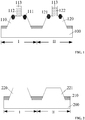
- Figure 1 illustrates a schematic cross-sectional view of a semiconductor device.
- the semiconductor device includes a substrate 100 and a plurality of fins protruding from the substrate 100.
- the substrate 100 includes a first region I and a second region II.
- the fin on the first region I of the substrate 100 is the first fin 110 and the fin on the second region II of the substrate 100 is the second fin 120.
- the first region I is used to form a core device and the second region II is used to form an IO device.
- the semiconductor device further includes a first gate electrode 112 in the first region I, a second gate electrode 122 in the second region II, a first source/drain region 111 on both sides of the first gate electrode 112, and a second source/drain region 121 on both sides of the second gate electrode 122.
- the IO device formed in the second region II may easily cause a gate leakage current phenomenon, so that the reliability of the semiconductor device needs to be improved.
- the first gate electrode 112 and the second gate electrode 122 are formed by the following processes: forming a gate electrode layer across the first fin 110; forming a hard mask layer 113 on the gate electrode layer; and etching the gate electrode layer with the hard mask layer 113 as a mask to form a first gate electrode 112 across the first fin 110 and a second gate electrode 122 across the second fin 120, respectively.
- the first gate electrode 112 covers a portion of the top and sidewall of the first fin 110 and the second gate electrode 122 covers a portion of the top and sidewall of the second fin 120.
- the first gate electrode 112 and the second gate electrode 122 can be affected by the etching parameters, such as the amount of over-etching.
- the first gate electrode 112 and the second gate electrode 122 may have a footing structure when the over-etching is insufficient.
- the footing structure of the first gate electrode 112 and the second gate electrode 122 has a stepped sidewall, including a lower step portion on the fins and an upper step portion on the lower step portion.
- the size of the lower step portion is larger than the size of the upper step portion along the direction parallel to the substrate 100.
- the working current of the IO device is relatively large. Because the second gate electrode 122 has a footing structure, the distance between the second gate electrode 122 and the second source/drain region 121 is small. Thus, the gate can easily be punched through, causing a leakage current problem.
- a base substrate in the present invention, includes a first region for forming a first transistor and a second region for forming a second transistor.
- the working current of the first transistor is smaller than the working current of the second transistor.
- a gate electrode layer is further formed on the base substrate. The gate electrode layer is then etched to form a first gate electrode in the first region. After forming the first gate electrode, the gate electrode layer is etched to form a second gate electrode in the second region, with the second gate electrode having an undercut structure.
- a first source/drain doped region is then formed on the base substrate on both sides of the first gate electrode, and a second source/drain doped region is formed on the base substrate on both sides of the second gate electrode.
- a second gate electrode having an undercut structure at its bottom is formed.
- the undercut structure of the second gate electrode has a stepped sidewall, including a first step portion on the base substrate and a second step portion on the first step portion.
- the size of the second step portion is larger than the size of the first step portion.
- the distance between the second gate electrode and the second source/drain doped region is increased by making the width of the second gate electrode structure smaller than the top width. Therefore, the gate leakage current phenomenon can be suppressed even if the working current of the second transistor is relatively large, and the reliability of the semiconductor device is improved.
- Figure 13 illustrates an exemplary fabrication process of a semiconductor device consistent with the disclosed embodiments
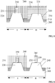
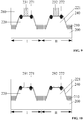
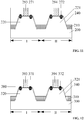
- Figures 2 ⁇ 11 illustrate schematic cross-sectional views of semiconductor devices corresponding to certain stages of the exemplary fabrication process consistent with the disclosed embodiments.
- a base substrate including a first region and a second region is provided (S101).
- a base substrate is provided, and the base substrate includes a first region I for forming a first transistor and a second region II for forming a second transistor.
- the working current of the first transistor is smaller than the working current of the second transistor.
- the first region I is used to form a core device, and the second region II is used to form an IO device.
- a FinFET device is formed as an example of the semiconductor device.
- the base substrate includes a substrate 200 and a plurality of fins on the substrate 200.
- the formed semiconductor device may be a planar device, and accordingly, the base substrate is a planar substrate.
- the base substrate includes a substrate 200 and a plurality of fins on the substrate 200.
- the fins include a first fin 220 on the first region I of the substrate 200 and a second fin 221 on the second region II of the substrate 200.
- the base substrate also includes an isolation structure 210, and the isolation structure 210 covers a portion of the sidewall surface of the first fin 220 and the second fin 221. The top of the isolation structure 210 is lower than the top of the first fin 220 and the second fin 221.
- the isolation structure 210 may electrically isolate the first fin 220 from the adjacent second fin 221.
- the substrate 200 may be made of silicon, germanium, silicon germanium, silicon carbide, gallium arsenide, or indium gallium oxide.
- the substrate 200 may also be made of a silicon-on-insulator (SOI) substrate or a germanium-on-insulator (GOI) substrate.
- SOI silicon-on-insulator
- GOI germanium-on-insulator
- the first fin 220 and the second fin 221 may be made of silicon, germanium, silicon germanium, silicon carbide, gallium arsenide, or indium gallium
- the isolation structure 210 may be made of silicon oxide, silicon nitride, or silicon oxynitride.
- the substrate 200 is a silicon substrate; the first fin 220 and the second fin 221 are made of silicon; and the isolation structure 210 is made of silicon oxide.
- the substrate 200, the first fin 220, and the second fin 221 are formed by the following processes: providing an initial substrate; forming a patterned hard mask layer on surface of the initial substrate; etching the initial substrate with the hard mask layer as a mask and the etched initial substrate being the substrate 200; the protrusion on the first region I of the surface of the substrate 200 being the first fin 220 and the protrusion on the second region II of the surface of the substrate 200 being the second fin 221; and removing the hard mask layer after forming the first fin 220 and the second fin 221.
- the process of forming the hard mask layer includes: first forming an initial hard mask layer; forming a patterned photoresist layer on the surface of the initial hard mask layer; etching the initial hard mask layer by using the patterned photoresist layer as a mask to form a hard mask layer on the surface of the initial substrate; and removing the patterned photoresist layer.
- the process of forming the hard mask layer may also include a self-aligned double patterned process, a self-aligned triple patterned process, a self-aligned double double patterned process.
- the double patterned process may be a litho-etch-litho-etch (LELE) process or a litho-litho-etch (LLE) process.
- the processes of forming the isolation structure 210 include: forming an isolation film covering the first fin 220 and the second fin 221 on the substrate 200, with the top of the isolation film being higher than the top of the first fin 220 and the second fin 221; subjecting the top of the isolation film to a planarization process; after the planarization treatment, etching-back a partial thickness of the isolation film to form the isolation structure 210 on the substrate 200.
- a gate electrode layer is formed on the base substrate (S102). As shown in Figure 3 , a gate electrode layer 230 is formed on the base substrate, and the gate electrode layer 230 covers the first fin 220 and the second fin 221.
- the gate electrode layer 230 may be made of polysilicon or a metal, and the metal may be one or more of Ti, Ta, TiN, TaN, TiAl, TiAIN, Cu, Al, W, Ag or Au.
- a gate dielectric layer 240 may also be formed on the base substrate before forming the gate electrode layer 230.
- the gate dielectric layer 240 is made of a high-k gate dielectric material.
- An interfacial layer may also be formed between the gate dielectric layer 240 and the first fin 220.
- the interfacial layer is made of silicon oxide.
- a first gate electrode is formed in the first region of the base substrate by etching the gate electrode layer (S103).
- the gate electrode layer 230 is etched, and a first gate electrode 231 is formed in the first region I.
- the formed first gate electrode 231 is across the first fin 220 and covers a portion of the top and sidewall of the first fin 220.
- the first gate electrode 231 may be made of polysilicon or a metal, and the metal may be one or more of Ti, Ta, TiN, TaN, TiAl, TiAIN, Cu, Al, W, Ag or Au.
- the process of forming the first gate electrode 231 includes: forming a hard mask layer 250 on the gate electrode layer 230, with the hard mask layer 250 defining the pattern of the first gate electrode 231 to be formed; using the hard mask layer 250 as a mask, patterning the gate electrode layer 230 in the first region I to form a first gate electrode 231 in the first region I.
- the bottom of the first gate electrode 231 has a footing structure due to over-etching in the etching process. That is, the footing structure of the first gate electrode 231 has a stepped sidewall including a third step portion on the base substrate and a fourth step portion on the third step portion. The size of the third step portion is greater than the size of the fourth step portion along the direction parallel to the base substrate.
- the size of the footing structure of the first gate electrode 231 may be in a range of 1 ⁇ 5 nm. Since the working current of the core device formed in the first region I is low, even if the first gate electrode 231 has a footing structure, the first gate electrode 231 is unlikely to be punched through.
- the first gate electrode 231 may also be in an undercut structure or a vertical structure, which may further overcome the gate leakage problem.
- the undercut structure of the first gate electrode 231 has a stepped sidewall, including a third step portion on the base substrate and a fourth step portion on the third step portion.
- the size of the third step portion is smaller than the size of the fourth step portion along a direction parallel to the base substrate.
- the width of the first gate electrode 231 is equal to the top width.
- the parameters of the etching process when forming the first gate electrode 231 are as follows: the etching gas is a mixed gas of CF 4 , SF 6 , N 2 and O 2 ; the gas flow rate of CF 4 is approximately 50 ⁇ 175 sccm; the gas flow rate of SF 6 is approximately 5 ⁇ 81 sccm; the gas flow rate of N 2 is approximately 6 ⁇ 75 sccm; the gas flow rate of the O 2 gas is approximately 1 ⁇ 25 sccm; the pressure is approximately 1mtorr ⁇ 150mtorr; the etching time is approximately 10 ⁇ 2000s; the voltage is approximately 50 ⁇ 300 V; and the RF power is approximately 200 ⁇ 500W.
- the etching gas is a mixed gas of CF 4 , SF 6 , N 2 and O 2 ; the gas flow rate of CF 4 is approximately 50 ⁇ 175 sccm; the gas flow rate of SF 6 is approximately 5 ⁇ 81 scc
- the portion of the hard mask layer 250 at the top of the first gate electrode 231 is retained, such that the hard mask layer 250 protects the top of the first gate electrode 231 during the subsequent process.
- the hard mask layer 250 may be made of silicon nitride, silicon oxynitride, silicon carbide, or boron nitride.
- the fabrication method further includes forming a second gate electrode in the second region (S104).
- the gate electrode layer 230 is etched to form the second gate electrode 232 in the second region II.
- the second gate electrode 232 has an undercut structure.
- the undercut structure of the second gate electrode 232 has a stepped sidewall, including a first step portion on the substrate and a second step portion on the first step portion.
- the size of the first step portion is smaller than the size of the second step portion along the direction parallel to the substrate.
- the second gate electrode 232 has an undercut structure.
- the size of the undercut structure of the second gate electrode 232 should be neither too large nor too small in the direction parallel to the substrate.
- the size of the undercut structure is too large, it is likely that the distance between the subsequently formed second source/drain doped region and the channel formed is insufficient, and the performance of the device is reduced.
- the size of the undercut structure may be in a range of 2 ⁇ 20 nm.
- the process of forming the second gate electrode 232 includes an over-etching process.
- the bottom of the second gate electrode 232 can have an undercut structure by controlling the amount of over-etching.
- the undercut structure is used to increase the distance between the source/drain and the bottom of the second gate electrode 232. Therefore, even if the working current of the IO device is relatively large, the gate leakage phenomenon can be suppressed, thereby improving the reliability of the semiconductor device.
- a second gate electrode 232 having an undercut structure is formed by an over-etching process.
- the process of forming the second gate electrode 232 includes:
- a photoresist layer 260 is formed on the hard mask layer 250, and the photoresist layer 260 covers the top and sidewalls of the first gate electrode 231 and the top of the hard mask layer 250 in the second region II.
- the photoresist layer 260 is patterned, and a portion of the photoresist layer 260 in the second region II is removed. The remaining photoresist layer 260 in the second region II defines the pattern of the second gate electrode 232 to be formed.
- the gate electrode layer 230 and the hard mask layer 250 in the second region II are etched to form the second gate electrode 232 in the second region II.
- the photoresist layer 260 in the first region I is a protective layer of the first gate electrode 231, covering the top and sidewalls of the first gate electrode 231.
- the etching parameters in the process of forming the second gate electrode 232 by over-etching include: the etching gas being a mixed gas of HBr, He and O 2 , the gas flow rate of HBr being 50 ⁇ 1000 sccm, the gas flow rate of He being 300 ⁇ 1500 sccm, the gas flow rate of O 2 being 1 ⁇ 20 sccm, the pressure being 30 ⁇ 250mtorr, the etching time being 10 ⁇ 200s, and the RF power being 700 ⁇ 3000 W.
- the photoresist layer 260 in the first region I and the second region II is removed, exposing the hard mask layer 250 at the top of the first gate electrode 231 and the second gate electrode 232.
- the process of removing the photoresist layer 260 (see Figure 6 ) in the first region I and the second region II is a dry etching process.
- the exposed hard mask layer 250 at the top of the first gate electrode 231 and the second gate electrode 232 is used to protect the top of the first gate electrode 231 and the second gate electrode 232, such that the top of the first gate electrode 231 and the second gate electrode 232 may not be damaged in the subsequent process.
- the fabrication method further includes forming a first source/drain doped region and a second source/drain doped region (S105).
- a first source/drain doped region 271 is formed on the base substrate on both sides of the first gate electrode 231, and the second source/drain doped region 272 is formed on the base substrate on both sides of the second gate electrode 232.
- the first source/drain doped region 271 and the second source/drain doped region 272 are doped with P-type ions or N-type ions.
- the process of forming the first source/drain doped region 271 includes: etching the first fin 220 on both sides of the first gate electrode 231 to form a first trench in the first fin 220 on both sides of the first gate electrode 231; forming a first source/drain doped region 271 that fills up the first trench; and doping P-type or N-type ions in the first source/drain doped region 271.
- the process of forming the second source/drain doped region 272 includes: etching the second fin 221 on both sides of the second gate electrode 232 to form a second trench in the second fin 221 on both sides of the second gate electrode 232; forming a second source/drain doped region 272 that fills up the second trench; and doping P-type or N-type ions in the second source/drain doped region 271.
- the first source/drain doped region 271 and the second source/drain doped region 272 are formed by a selective epitaxial process. Because the portion of the fin other than the first trench and the second trench is covered by the gate dielectric layer 240 and the lattice constant of the material of the gate dielectric layer 240 is significantly different from the lattice constant of the material of the first source/drain doped region 271 and the second source/drain doped region 272, the epitaxial growth of films in an undesired region is avoided.
- the first source/drain doped region 271 and the second source/drain doped region 272 are made of Si or SiC, and the first source/drain doped region 271 and the second source/drain doped region 272 are doped with N-type ions, with the N-type ions being P, As or Sb;
- the first source/drain doped region 271 and the second source/drain doped region 272 are made of Si or SiGe, and the first source/drain doped region 271 and the second source/drain doped region 272 are doped with P-type ions, with the P-type ions being B, Ga or In.
- the first source/drain doped region 271 and the second source/drain region 272 may provide a stretching stress to the channel region, increasing the carrier mobilities of the NMOS device; when the first source/drain doped region 271 and the second source/drain region 272 are made of SiGe, the first source/drain doped region 271 and the second source/drain doped region 272 may provide a compression stress to the channel region, increasing the carrier mobilities of the PMOS device.
- the semiconductor device is formed by a rear gate process, and the subsequent process further includes:
- an interlayer dielectric layer 280 is formed on the portion of the base substrate exposed by the first gate electrode 231 and the second gate electrode 232.
- the interlayer dielectric layer 280 covers the surface of the base substrate, the surface of the first source/drain doped region 271, the surface of the second source/drain doped region 272, the sidewall of the first gate electrode 231, and the sidewall of the second gate electrode 232.
- the process of forming the interlayer dielectric layer 280 includes: forming an interlayer dielectric film covering the base substrate, with the top of the interlayer dielectric film being higher than the top of the first gate electrode 231 and the second gate electrode 232; etching the interlayer dielectric film until the top of the first gate electrode 231 and the second gate electrode 232 is exposed to form an interlayer dielectric layer 280; and removing the hard mask layer 250 simultaneously when etching the interlayer dielectric film (as shown in Figure 8 ).
- first gate electrode 231 and the second gate electrode 232 are removed to form a first opening 291 and a second opening 292, respectively.
- the process of forming the first opening 291 and the second opening 292 includes: etch-removing the first gate electrode 231 and the second gate electrode 232; forming a first opening 291 in the interlayer dielectric layer 280 of the first region I and forming a second opening 292 in the interlayer dielectric layer 280 of the second region II.
- first opening 291 As shown in Figure 11 , the first opening 291 (As shown in Figure 10 ) and the second opening 292 (As shown in Figure 10 ) are filled with metal, forming a first metal gate 293 and a second metal gate 294, respectively.
- the second metal gate 294 is at the position of the second gate electrode 232 before being etched, the second metal gate 294 and the second gate electrode 232 have the same structure, i.e., an undercut structure.
- the undercut structure has a stepped sidewall, including a first step portion on the substrate and a second step portion on the first step portion.
- the size of the second step portion is larger than the size of the first step portion.
- An undercut structure is used to increase the distance between the source/drain region and the bottom of the second metal gate. Therefore, by making the width of the second metal gate structure smaller than the top width, the gate leakage phenomenon may be suppressed and the reliability of the semiconductor device may be enhanced.
- the present invention also provides a semiconductor device.
- Figure 12 illustrates a schematic view of an embodiment of the semiconductor device consistent with the present invention.
- the semiconductor device includes: a base substrate, and the base substrate includes a first region I having a first transistor and a second region II having a second transistor.
- the working current of the first transistor is smaller than the working current of the second transistor.
- the semiconductor device includes a first gate electrode 393 on the first region I of the substrate; a second gate electrode 394 on the second region II of the substrate, with the second gate electrode 394 having an undercut structure; a first source/drain doped region 371 in the base substrate on both sides of the first gate electrode 393; a second source/drain doped region 372 in the base substrate on both sides of the second gate electrode 394.
- the semiconductor device is a FinFET device.
- the base substrate includes a substrate 300 and a plurality of fins on the substrate 300.
- the fins include a first fin 320 on the first region I of the substrate 300 and a second fin 321 on the second region II of the substrate 300.
- the base substrate also includes an isolation structure 310, and the isolation structure 310 covers a portion of the sidewall surface of the first fin 320 and the second fin 321.
- the top of the isolation structure 310 is lower than the top of the first fin 320 and the second fin 321.
- the semiconductor device further includes an interlayer dielectric layer 380 on the first gate electrode 393, the second gate electrode 394, and the base substrate.
- the first gate electrode 393 is the first metal gate on the interlayer dielectric layer 380
- the second gate electrode 394 is the second metal gate on the interlayer dielectric layer.
- the first gate electrode 393 is made of a metal, and the metal may be one or more of Ti, Ta, TiN, TaN, TiAl, TiAIN, Cu, Al, W, Ag or Au.
- the bottom of the first gate electrode 393 has a footing structure. That is, the footing structure of the first gate electrode 393 has a stepped sidewall, including a third step portion on the base substrate and a fourth step portion on the third step portion. The size of the third step portion is larger than the size of the fourth step portion along a direction parallel to the substrate. The size of the footing structure of the first gate electrode 393 may be in a range of 1 to 5 nm. Since the working current of the core device formed in the first region I is relatively low, even if the first gate electrode 393 has a footing structure, the first gate electrode 393 may not be easily punched through to cause a leakage current problem.
- the first gate electrode 393 may also have an undercut structure or a vertical structure, which may further suppress the gate leakage phenomenon.
- the undercut structure of the first gate electrode 393 has a stepped sidewall, including a third step portion on the base substrate and a fourth step portion on the third step portion.
- the size of the third step portion is smaller than the size of the fourth step portion in a direction parallel to the base substrate.
- the width of the first gate electrode 393 is equal to the top width.
- the undercut structure of the second gate electrode 394 has a stepped sidewall, including a first step portion on the substrate and a second step portion on the first step portion.
- the size of the first step portion is smaller than the size of the second step portion in a direction parallel to the base substrate.
- the second gate electrode 394 has an undercut structure.
- the size of the undercut structure at the bottom of the second gate electrode 394 may be in a range of 2 to 20 nm.
- the size of the undercut structure of the second gate electrode 394 may be neither too large nor too small in the direction parallel to the base substrate. That is, the size of the undercut structure may be in a range of 2 to 20 nm. When the size of the undercut structure is larger than 20 nm, the extension from the source/drain doped region to the channel is likely to be insufficient, and the performance of the device is reduced. When the size of the undercut structure is less than 2 nm, a leakage current from the gate to the epitaxial layer may occur.
- the undercut structure is used to increase the distance between the second source/drain doped region 372 and the bottom of the second gate electrode 394. Therefore, even if the working current of the IO device is large, the gate leakage phenomenon can be suppressed and the reliability of the semiconductor device may be improved.
- the first source/drain doped region 371 is doped with P-type ions or N-type ions.
- the second source/drain doped region 372 is doped with P-type ions or N-type ions.
- the disclosed semiconductor device may include a FinFET device.
- the FinFET device may include a gate structure having a core device in the first region and an IO device in the second region.
- the core device has a footing structure while the IO device has an undercut structure. Since an undercut structure of the IO device increases the distance between the bottom of the second gate electrode and the second source/drain doped region in the second region, the gate leakage phenomenon of the semiconductor device is less likely to occur. Therefore, the reliability of the IO device is improved and the performance of the core device is also enhanced.
- the fabrication method in the present invention is advantageous.
- the fabrication method of a semiconductor device includes providing a base substrate.
- the base substrate includes a first region for forming a first transistor and a second region for forming a second transistor.
- the working current of the first transistor is smaller than the working current of the second transistor.
- a first gate electrode is formed in the first region and a second gate electrode is formed in the second region.
- the width of the second gate electrode is smaller than the top width, such that the second gate electrode has an undercut structure.
- a second source/drain doped region is formed in the base substrate on both sides of the second gate electrode.
Landscapes
- Chemical & Material Sciences (AREA)
- Chemical Kinetics & Catalysis (AREA)
- General Chemical & Material Sciences (AREA)
- Engineering & Computer Science (AREA)
- Materials Engineering (AREA)
- Mechanical Engineering (AREA)
- Metallurgy (AREA)
- Organic Chemistry (AREA)
- Insulated Gate Type Field-Effect Transistor (AREA)
- Metal-Oxide And Bipolar Metal-Oxide Semiconductor Integrated Circuits (AREA)
Abstract
Description
- This application claims the priority of Chinese patent application No.
201611125155.3, filed on December 08, 2016 - The present invention generally relates to the field of semiconductor manufacturing technologies and, more particularly, relates to a semiconductor device and a fabrication method thereof.
- With the rapid development of semiconductor technologies, the feature size of semiconductor devices continues to decrease, making the integration degree of integrated circuits higher and higher. This also sets higher requirements for the performance of devices.
- At present, as the size of the metal oxide semiconductor field effect transistor (MOSFET) becomes smaller, the channel length of the MOSFET needs to be continuously shortened to adapt to a reduced process node. A shorter channel length is advantageous to increase the die density of a chip and increase the switching speed of a MOSFET.
- However, when the channel length of devices becomes shorter, the distance between the source and drain of devices is also shortened. Therefore, the controlling capability of gate to channel is degraded and the pinch off of channel by the gate voltage becomes more difficult, causing a subthreshold leakage current phenomenon. That is, the short-channel effects (SCEs) can occur more easily, which has become a crucial technical issue.
- To better adapt to a scaled-down size of devices, semiconductor technologies are gradually developed from the planar MOSFET to the more efficient three-dimensional transistors, such as fin field effect transistor (FinFET) with better channel controlling capabilities.
- A FinFET device often includes a core device and an input/output (IO) device. Because the working current of an IO device is relatively large, the gate leakage current phenomenon is more likely to occur in a FinFET device.
- Therefore, there is a need to resolve the gate leakage current problem of semiconductor devices and to improve the reliability of semiconductor devices.
- It is an object of the present invention to provide a method for fabricating a semiconductor device and a semiconductor device which may solve one or more problems in the prior art discussed above, in particular by which or in which the gate leakage current problem of prior art semiconductor devices is resolved or at least reduced and thus the reliability of semiconductor devices can be further improved.
- The object is achieved by the features of the respective independent claims. Further embodiments are defined in the respective dependent claims.
- A first aspect of the present invention provides a method for fabricating a semiconductor device. The fabrication method includes providing a base substrate including a first region for forming a first transistor and a second region for forming a second transistor. The working current of the first transistor is smaller than the working current of the second transistor. The fabrication method further includes: forming a gate electrode layer on the base substrate; etching the gate electrode layer to form a first gate electrode in the first region; after forming the first gate electrode, etching the gate electrode layer to form a second gate electrode in the second region, with the second gate electrode having an undercut structure; forming a first source/drain doped region in the base substrate on both sides of the first gate electrode; and forming a second source/drain doped region in the base substrate on both sides of the second gate electrode.
- Preferably, the base substrate includes a substrate and a plurality of fins on the substrate.
- Preferably, the first gate electrode is formed across the fin in the first region, covering a portion of a top and sidewall of the fin in the first region.
- Preferably, the second gate electrode is formed across the fin in the second region, covering a portion of a top and sidewall of the fin in the second region.
- Preferably, the first source/drain doped region is formed within the fin in the first region on both sides of the first gate electrode.
- Preferably, the second source/drain doped region is formed within the fin in the second region on both sides of the second gate electrode.
- Preferably, the method further comprises: forming an interlayer dielectric layer on portions of the base substrate exposed by the first gate electrode and the second gate electrode; removing the first gate electrode and the second gate electrode to respectively form a first opening and a second opening in the interlayer dielectric layer; and filling the first opening and the second opening with a metal to form a first metal gate electrode and a second metal gate electrode.
- Preferably, the first gate electrode has a footing structure.
- Preferably, wherein forming the second gate electrode comprises: forming a photoresist layer on the first gate electrode and on the gate electrode layer in the second region; and etching the gate electrode layer using the photoresist layer as an etching mask to form the second gate electrode.
- Preferably, etching the gate electrode layer to form the first gate electrode in the first region comprises: forming a hard mask layer on the gate electrode layer of the first region; and etching the gate electrode layer using the hard mask layer as an etching mask to form the first gate electrode.
- Preferably, the first transistor formed in the first region includes a core device.
- Preferably, the second transistor formed in the second region includes an IO device.
- Preferably, the undercut structure has a stepped sidewall including a first step portion on the base substrate and a second step portion on the first step portion. Preferably, the first step portion has a smaller size than the second step portion in a direction parallel to a surface of the base substrate.
- Preferably, the footing structure has a stepped sidewall including a third step portion on the base substrate and a fourth step portion on the third step portion. Preferably, the third step portion has a larger size than the fourth step portion in a direction parallel to a surface of the base substrate.
- Preferably, etching process parameters for forming the second gate electrode comprise: an etching gas including a mixed gas of HBr, He and 02, a gas flow rate of HBr being approximately 50 ∼ 1000 sccm, a gas flow rate of He being approximately 300 ∼ 1500 sccm, a gas flow rate of 02 being approximately 1 ∼ 20 sccm, a pressure of approximately 30 ∼ 250 mtorr, an etching time of approximately 10 ∼ 200s, and a RF power of approximately 700 ∼ 3000 W.
- Preferably, etching process parameters for forming the first gate electrode comprise: an etching gas including a mixed gas of CF4, SF6, N2 and 02, a gas flow rate of CF4 being approximately 50 ∼ 175 sccm, a gas flow rate of SF6 being approximately 5 ∼ 81 sccm, a gas flow rate of N2 being approximately 6 ∼ 75 sccm, a gas flow rate of 02 being approximately 1 ∼ 25 sccm, a pressure of approximately 1 ∼ 150 mtorr, an etching time of approximately 10 ∼ 2000s, a voltage of approximately 50 ∼ 300 V, and a RF power of approximately 200 ∼ 500 W.
- Preferably, forming the first source/drain doped region comprises: etching a portion of the base substrate on both sides of the first gate electrode to form a first trench in the base substrate on both sides of the first gate electrode; and forming a source/drain epitaxial doped layer filling the first trench, the source/drain epitaxial doped layer being doped with P-type ions or N-type ions.
- Preferably, forming the second source/drain doped region comprises: etching a portion of the base substrate on both sides of the second gate electrode to form a second trench in the base substrate on both sides of the second gate electrode; and forming a source/drain epitaxial doped layer filling the second trench, the source/drain epitaxial doped layer being doped with P-type ions or N-type ions.
- A second aspect of the present invention provides a semiconductor device. The semiconductor device includes a base substrate, and the base substrate includes a first region having a first transistor and a second region having a second transistor. The working current of the first transistor is smaller than the working current of the second transistor. The semiconductor device further includes a first gate electrode on the first region of the base substrate; a second gate electrode on the second region of the base substrate, with the second gate electrode having an undercut structure; a first source/drain doped region in the base substrate on both sides of the first gate electrode; and a second source/drain doped region in the base substrate on both sides of the second gate electrode.
- Preferably, the base substrate includes a substrate and a plurality of fins on the substrate.
- Preferably, the first gate electrode is formed across the fin in the first region, covering a portion of the top and sidewall of the fin in the first region.
- Preferably, the second gate electrode is formed across the fin in the second region, covering a portion of the top and sidewall of the fins in the second region.
- Preferably, the first source/drain doped region formed is within the fin in the first region on both sides of the first gate electrode.
- Preferably, the second source/drain doped region is formed within the fin in the second region on both sides of the second gate electrode.
- Preferably, the semiconductor device further comprises: an interlayer dielectric layer on the first gate electrode, the second gate electrode, and the base substrate; the first gate electrode being a first metal gate in the interlayer dielectric layer; and the second gate electrode being a second metal gate in the interlayer dielectric layer.
- Preferably, the first gate electrode has a footing structure.
- Preferably, the first transistor formed in the first region includes a core device.
- Preferably, the second transistor formed in the second region includes an IO device.
- Preferably, the undercut structure has a stepped sidewall including a first step portion on the base substrate and a second step portion on the first step portion. Preferably, the first step portion has a smaller size than the second step portion in a direction parallel to the base substrate.
- Preferably, the footing structure has a stepped sidewall including a third step portion on the base substrate and a fourth step portion on the third step portion. Preferably, the third step portion has a larger size than the fourth step portion in a direction parallel to a surface of the base substrate.
- A semiconductor device according to the second aspect of the present invention may be obtained by a method according to the first aspect of the present invention.
- Other aspects of the present invention can be understood by those skilled in the art in light of the description, the claims, and the drawings of the present invention.
-
-
Figure 1 illustrates a schematic view of a semiconductor device; and -
Figures 2∼11 illustrate schematic structural views of a semiconductor device corresponding to certain stages of a fabrication process consistent with various disclosed embodiments; and -
Figure 12 illustrates a schematic structural view of an exemplary semiconductor device consistent with various disclosed embodiments; and -
Figure 13 illustrates an exemplary fabricating process of a semiconductor device consistent with the disclosed embodiments. - Reference will now be made in detail to the exemplary embodiments of the invention, which are illustrated in the accompanying drawings. Wherever possible, the same reference numbers will be used throughout the drawings to refer to the same or similar parts.
-
Figure 1 illustrates a schematic cross-sectional view of a semiconductor device. As shown inFigure 1 , the semiconductor device includes asubstrate 100 and a plurality of fins protruding from thesubstrate 100. Thesubstrate 100 includes a first region I and a second region II. The fin on the first region I of thesubstrate 100 is thefirst fin 110 and the fin on the second region II of thesubstrate 100 is thesecond fin 120. The first region I is used to form a core device and the second region II is used to form an IO device. - The semiconductor device further includes a
first gate electrode 112 in the first region I, asecond gate electrode 122 in the second region II, a first source/drain region 111 on both sides of thefirst gate electrode 112, and a second source/drain region 121 on both sides of thesecond gate electrode 122. - The IO device formed in the second region II may easily cause a gate leakage current phenomenon, so that the reliability of the semiconductor device needs to be improved.
- The
first gate electrode 112 and thesecond gate electrode 122 are formed by the following processes: forming a gate electrode layer across thefirst fin 110; forming ahard mask layer 113 on the gate electrode layer; and etching the gate electrode layer with thehard mask layer 113 as a mask to form afirst gate electrode 112 across thefirst fin 110 and asecond gate electrode 122 across thesecond fin 120, respectively. Thefirst gate electrode 112 covers a portion of the top and sidewall of thefirst fin 110 and thesecond gate electrode 122 covers a portion of the top and sidewall of thesecond fin 120. Thefirst gate electrode 112 and thesecond gate electrode 122 can be affected by the etching parameters, such as the amount of over-etching. For example, thefirst gate electrode 112 and thesecond gate electrode 122 may have a footing structure when the over-etching is insufficient. - The footing structure of the
first gate electrode 112 and thesecond gate electrode 122 has a stepped sidewall, including a lower step portion on the fins and an upper step portion on the lower step portion. The size of the lower step portion is larger than the size of the upper step portion along the direction parallel to thesubstrate 100. - The working current of the IO device is relatively large. Because the
second gate electrode 122 has a footing structure, the distance between thesecond gate electrode 122 and the second source/drain region 121 is small. Thus, the gate can easily be punched through, causing a leakage current problem. - In the present invention, a base substrate is provided, and the base substrate includes a first region for forming a first transistor and a second region for forming a second transistor. The working current of the first transistor is smaller than the working current of the second transistor. A gate electrode layer is further formed on the base substrate. The gate electrode layer is then etched to form a first gate electrode in the first region. After forming the first gate electrode, the gate electrode layer is etched to form a second gate electrode in the second region, with the second gate electrode having an undercut structure. A first source/drain doped region is then formed on the base substrate on both sides of the first gate electrode, and a second source/drain doped region is formed on the base substrate on both sides of the second gate electrode.
- In the present invention, a second gate electrode having an undercut structure at its bottom is formed. The undercut structure of the second gate electrode has a stepped sidewall, including a first step portion on the base substrate and a second step portion on the first step portion. The size of the second step portion is larger than the size of the first step portion. The distance between the second gate electrode and the second source/drain doped region is increased by making the width of the second gate electrode structure smaller than the top width. Therefore, the gate leakage current phenomenon can be suppressed even if the working current of the second transistor is relatively large, and the reliability of the semiconductor device is improved.
-
Figure 13 illustrates an exemplary fabrication process of a semiconductor device consistent with the disclosed embodiments; andFigures 2∼11 illustrate schematic cross-sectional views of semiconductor devices corresponding to certain stages of the exemplary fabrication process consistent with the disclosed embodiments. - As shown in
Figure 13 , at the beginning of the fabrication process, a base substrate including a first region and a second region is provided (S101). - As shown in
Figure 2 , a base substrate is provided, and the base substrate includes a first region I for forming a first transistor and a second region II for forming a second transistor. The working current of the first transistor is smaller than the working current of the second transistor. - The first region I is used to form a core device, and the second region II is used to form an IO device.
- In the present invention, a FinFET device is formed as an example of the semiconductor device. For a FinFET device, the base substrate includes a
substrate 200 and a plurality of fins on thesubstrate 200. In other embodiments, the formed semiconductor device may be a planar device, and accordingly, the base substrate is a planar substrate. - In one embodiment, the base substrate includes a
substrate 200 and a plurality of fins on thesubstrate 200. The fins include afirst fin 220 on the first region I of thesubstrate 200 and asecond fin 221 on the second region II of thesubstrate 200. The base substrate also includes anisolation structure 210, and theisolation structure 210 covers a portion of the sidewall surface of thefirst fin 220 and thesecond fin 221. The top of theisolation structure 210 is lower than the top of thefirst fin 220 and thesecond fin 221. - The
isolation structure 210 may electrically isolate thefirst fin 220 from the adjacentsecond fin 221. - The
substrate 200 may be made of silicon, germanium, silicon germanium, silicon carbide, gallium arsenide, or indium gallium oxide. Thesubstrate 200 may also be made of a silicon-on-insulator (SOI) substrate or a germanium-on-insulator (GOI) substrate. Thefirst fin 220 and thesecond fin 221 may be made of silicon, germanium, silicon germanium, silicon carbide, gallium arsenide, or indium gallium, and theisolation structure 210 may be made of silicon oxide, silicon nitride, or silicon oxynitride. In one embodiment, thesubstrate 200 is a silicon substrate; thefirst fin 220 and thesecond fin 221 are made of silicon; and theisolation structure 210 is made of silicon oxide. - In one embodiment, the
substrate 200, thefirst fin 220, and thesecond fin 221 are formed by the following processes: providing an initial substrate; forming a patterned hard mask layer on surface of the initial substrate; etching the initial substrate with the hard mask layer as a mask and the etched initial substrate being thesubstrate 200; the protrusion on the first region I of the surface of thesubstrate 200 being thefirst fin 220 and the protrusion on the second region II of the surface of thesubstrate 200 being thesecond fin 221; and removing the hard mask layer after forming thefirst fin 220 and thesecond fin 221. - In particular, the process of forming the hard mask layer includes: first forming an initial hard mask layer; forming a patterned photoresist layer on the surface of the initial hard mask layer; etching the initial hard mask layer by using the patterned photoresist layer as a mask to form a hard mask layer on the surface of the initial substrate; and removing the patterned photoresist layer. In other embodiments, the process of forming the hard mask layer may also include a self-aligned double patterned process, a self-aligned triple patterned process, a self-aligned double double patterned process. The double patterned process may be a litho-etch-litho-etch (LELE) process or a litho-litho-etch (LLE) process.
- The processes of forming the
isolation structure 210 include: forming an isolation film covering thefirst fin 220 and thesecond fin 221 on thesubstrate 200, with the top of the isolation film being higher than the top of thefirst fin 220 and thesecond fin 221; subjecting the top of the isolation film to a planarization process; after the planarization treatment, etching-back a partial thickness of the isolation film to form theisolation structure 210 on thesubstrate 200. - Returning to
Figure 13 , after providing the base substrate, a gate electrode layer is formed on the base substrate (S102). As shown inFigure 3 , agate electrode layer 230 is formed on the base substrate, and thegate electrode layer 230 covers thefirst fin 220 and thesecond fin 221. - The
gate electrode layer 230 may be made of polysilicon or a metal, and the metal may be one or more of Ti, Ta, TiN, TaN, TiAl, TiAIN, Cu, Al, W, Ag or Au. - A
gate dielectric layer 240 may also be formed on the base substrate before forming thegate electrode layer 230. Thegate dielectric layer 240 is made of a high-k gate dielectric material. - An interfacial layer may also be formed between the
gate dielectric layer 240 and thefirst fin 220. The interfacial layer is made of silicon oxide. - Returning to
Figure 13 , after forming the gate electrode layer, a first gate electrode is formed in the first region of the base substrate by etching the gate electrode layer (S103). - As shown in
Figure 4 , thegate electrode layer 230 is etched, and afirst gate electrode 231 is formed in the first region I. - In one embodiment, since the base substrate includes the
substrate 200 and fins, the formedfirst gate electrode 231 is across thefirst fin 220 and covers a portion of the top and sidewall of thefirst fin 220. - The
first gate electrode 231 may be made of polysilicon or a metal, and the metal may be one or more of Ti, Ta, TiN, TaN, TiAl, TiAIN, Cu, Al, W, Ag or Au. - The process of forming the
first gate electrode 231 includes: forming ahard mask layer 250 on thegate electrode layer 230, with thehard mask layer 250 defining the pattern of thefirst gate electrode 231 to be formed; using thehard mask layer 250 as a mask, patterning thegate electrode layer 230 in the first region I to form afirst gate electrode 231 in the first region I. In one embodiment, the bottom of thefirst gate electrode 231 has a footing structure due to over-etching in the etching process. That is, the footing structure of thefirst gate electrode 231 has a stepped sidewall including a third step portion on the base substrate and a fourth step portion on the third step portion. The size of the third step portion is greater than the size of the fourth step portion along the direction parallel to the base substrate. The size of the footing structure of thefirst gate electrode 231 may be in a range of 1∼5 nm. Since the working current of the core device formed in the first region I is low, even if thefirst gate electrode 231 has a footing structure, thefirst gate electrode 231 is unlikely to be punched through. - In other embodiments, the
first gate electrode 231 may also be in an undercut structure or a vertical structure, which may further overcome the gate leakage problem. - When the
first gate electrode 231 has an undercut structure, the undercut structure of thefirst gate electrode 231 has a stepped sidewall, including a third step portion on the base substrate and a fourth step portion on the third step portion. The size of the third step portion is smaller than the size of the fourth step portion along a direction parallel to the base substrate. - When the
first gate electrode 231 has a vertical structure, the width of thefirst gate electrode 231 is equal to the top width. - In one embodiment, the parameters of the etching process when forming the
first gate electrode 231 are as follows: the etching gas is a mixed gas of CF4, SF6, N2 and O2; the gas flow rate of CF4 is approximately 50 ∼ 175 sccm; the gas flow rate of SF6 is approximately 5 ∼ 81 sccm; the gas flow rate of N2 is approximately 6 ∼ 75 sccm; the gas flow rate of the O2 gas is approximately 1 ∼ 25 sccm; the pressure is approximately 1mtorr ∼ 150mtorr; the etching time is approximately 10 ∼ 2000s; the voltage is approximately 50 ∼ 300 V; and the RF power is approximately 200 ∼ 500W. - In one embodiment, the portion of the
hard mask layer 250 at the top of thefirst gate electrode 231 is retained, such that thehard mask layer 250 protects the top of thefirst gate electrode 231 during the subsequent process. Thehard mask layer 250 may be made of silicon nitride, silicon oxynitride, silicon carbide, or boron nitride. - Returning to
Figure 13 , after forming the first gate electrode, the fabrication method further includes forming a second gate electrode in the second region (S104). - As shown in
Figures 5 ∼ 7 , after forming thefirst gate electrode 231, thegate electrode layer 230 is etched to form thesecond gate electrode 232 in the second region II. Thesecond gate electrode 232 has an undercut structure. - In one embodiment, the undercut structure of the
second gate electrode 232 has a stepped sidewall, including a first step portion on the substrate and a second step portion on the first step portion. The size of the first step portion is smaller than the size of the second step portion along the direction parallel to the substrate. Thesecond gate electrode 232 has an undercut structure. - The size of the undercut structure of the
second gate electrode 232 should be neither too large nor too small in the direction parallel to the substrate. When the size of the undercut structure is too large, it is likely that the distance between the subsequently formed second source/drain doped region and the channel formed is insufficient, and the performance of the device is reduced. When the size of the undercut structure is too small, there will be a leakage current from the gate to the epitaxial layer. Therefore, in one embodiment, the size of the undercut structure may be in a range of 2 ∼ 20 nm. - The process of forming the
second gate electrode 232 includes an over-etching process. The bottom of thesecond gate electrode 232 can have an undercut structure by controlling the amount of over-etching. The undercut structure is used to increase the distance between the source/drain and the bottom of thesecond gate electrode 232. Therefore, even if the working current of the IO device is relatively large, the gate leakage phenomenon can be suppressed, thereby improving the reliability of the semiconductor device. - In the present invention, a
second gate electrode 232 having an undercut structure is formed by an over-etching process. Specifically, the process of forming thesecond gate electrode 232 includes: - As shown in
Figure 5 , aphotoresist layer 260 is formed on thehard mask layer 250, and thephotoresist layer 260 covers the top and sidewalls of thefirst gate electrode 231 and the top of thehard mask layer 250 in the second region II. - As shown in
Figure 6 , thephotoresist layer 260 is patterned, and a portion of thephotoresist layer 260 in the second region II is removed. The remainingphotoresist layer 260 in the second region II defines the pattern of thesecond gate electrode 232 to be formed. Using the patternedphotoresist layer 260 as a mask, thegate electrode layer 230 and thehard mask layer 250 in the second region II are etched to form thesecond gate electrode 232 in the second region II. - When etching to form the
second gate electrode 232, thephotoresist layer 260 in the first region I is a protective layer of thefirst gate electrode 231, covering the top and sidewalls of thefirst gate electrode 231. - In one embodiment, the etching parameters in the process of forming the
second gate electrode 232 by over-etching include: the etching gas being a mixed gas of HBr, He and O2, the gas flow rate of HBr being 50 ∼ 1000 sccm, the gas flow rate of He being 300 ∼ 1500 sccm, the gas flow rate of O2 being 1 ∼ 20 sccm, the pressure being 30 ∼ 250mtorr, the etching time being 10 ∼ 200s, and the RF power being 700 ∼ 3000 W. - As shown in
Figure 7 , the photoresist layer 260 (seeFigure 6 ) in the first region I and the second region II is removed, exposing thehard mask layer 250 at the top of thefirst gate electrode 231 and thesecond gate electrode 232. - The process of removing the photoresist layer 260 (see
Figure 6 ) in the first region I and the second region II is a dry etching process. The exposedhard mask layer 250 at the top of thefirst gate electrode 231 and thesecond gate electrode 232 is used to protect the top of thefirst gate electrode 231 and thesecond gate electrode 232, such that the top of thefirst gate electrode 231 and thesecond gate electrode 232 may not be damaged in the subsequent process. - Returning to
Figure 13 , after forming the second gate electrode, the fabrication method further includes forming a first source/drain doped region and a second source/drain doped region (S105). - As shown in
Figure 8 , a first source/drain dopedregion 271 is formed on the base substrate on both sides of thefirst gate electrode 231, and the second source/drain dopedregion 272 is formed on the base substrate on both sides of thesecond gate electrode 232. - The first source/drain doped
region 271 and the second source/drain dopedregion 272 are doped with P-type ions or N-type ions. - In one embodiment, the process of forming the first source/drain doped
region 271 includes: etching thefirst fin 220 on both sides of thefirst gate electrode 231 to form a first trench in thefirst fin 220 on both sides of thefirst gate electrode 231; forming a first source/drain dopedregion 271 that fills up the first trench; and doping P-type or N-type ions in the first source/drain dopedregion 271. The process of forming the second source/drain dopedregion 272 includes: etching thesecond fin 221 on both sides of thesecond gate electrode 232 to form a second trench in thesecond fin 221 on both sides of thesecond gate electrode 232; forming a second source/drain dopedregion 272 that fills up the second trench; and doping P-type or N-type ions in the second source/drain dopedregion 271. - In one embodiment, the first source/drain doped
region 271 and the second source/drain dopedregion 272 are formed by a selective epitaxial process. Because the portion of the fin other than the first trench and the second trench is covered by thegate dielectric layer 240 and the lattice constant of the material of thegate dielectric layer 240 is significantly different from the lattice constant of the material of the first source/drain dopedregion 271 and the second source/drain dopedregion 272, the epitaxial growth of films in an undesired region is avoided. - When the formed FinFET is an NMOS device, the first source/drain doped
region 271 and the second source/drain dopedregion 272 are made of Si or SiC, and the first source/drain dopedregion 271 and the second source/drain dopedregion 272 are doped with N-type ions, with the N-type ions being P, As or Sb; when the formed FinFET is a PMOS device, the first source/drain dopedregion 271 and the second source/drain dopedregion 272 are made of Si or SiGe, and the first source/drain dopedregion 271 and the second source/drain dopedregion 272 are doped with P-type ions, with the P-type ions being B, Ga or In. - When the first source/drain doped
region 271 and the second source/drain region 272 are made of SiC, the first source/drain dopedregion 271 and the second source/drain dopedregion 272 may provide a stretching stress to the channel region, increasing the carrier mobilities of the NMOS device; when the first source/drain dopedregion 271 and the second source/drain region 272 are made of SiGe, the first source/drain dopedregion 271 and the second source/drain dopedregion 272 may provide a compression stress to the channel region, increasing the carrier mobilities of the PMOS device. - In one exemplary embodiment, the semiconductor device is formed by a rear gate process, and the subsequent process further includes:
- As shown in
Figure 9 , aninterlayer dielectric layer 280 is formed on the portion of the base substrate exposed by thefirst gate electrode 231 and thesecond gate electrode 232. - The
interlayer dielectric layer 280 covers the surface of the base substrate, the surface of the first source/drain dopedregion 271, the surface of the second source/drain dopedregion 272, the sidewall of thefirst gate electrode 231, and the sidewall of thesecond gate electrode 232. - In the present embodiment, the process of forming the
interlayer dielectric layer 280 includes: forming an interlayer dielectric film covering the base substrate, with the top of the interlayer dielectric film being higher than the top of thefirst gate electrode 231 and thesecond gate electrode 232; etching the interlayer dielectric film until the top of thefirst gate electrode 231 and thesecond gate electrode 232 is exposed to form aninterlayer dielectric layer 280; and removing thehard mask layer 250 simultaneously when etching the interlayer dielectric film (as shown inFigure 8 ). - As shown in
Figure 10 , thefirst gate electrode 231 and thesecond gate electrode 232 are removed to form afirst opening 291 and asecond opening 292, respectively. - In one embodiment, the process of forming the
first opening 291 and thesecond opening 292 includes: etch-removing thefirst gate electrode 231 and thesecond gate electrode 232; forming afirst opening 291 in theinterlayer dielectric layer 280 of the first region I and forming asecond opening 292 in theinterlayer dielectric layer 280 of the second region II. - As shown in
Figure 11 , the first opening 291 (As shown inFigure 10 ) and the second opening 292 (As shown inFigure 10 ) are filled with metal, forming afirst metal gate 293 and asecond metal gate 294, respectively. - Since the
second metal gate 294 is at the position of thesecond gate electrode 232 before being etched, thesecond metal gate 294 and thesecond gate electrode 232 have the same structure, i.e., an undercut structure. - After forming the semiconductor device, since the
second metal gate 294 has an undercut structure, the undercut structure has a stepped sidewall, including a first step portion on the substrate and a second step portion on the first step portion. The size of the second step portion is larger than the size of the first step portion. An undercut structure is used to increase the distance between the source/drain region and the bottom of the second metal gate. Therefore, by making the width of the second metal gate structure smaller than the top width, the gate leakage phenomenon may be suppressed and the reliability of the semiconductor device may be enhanced. - Accordingly, the present invention also provides a semiconductor device.
-
Figure 12 illustrates a schematic view of an embodiment of the semiconductor device consistent with the present invention. - The semiconductor device includes: a base substrate, and the base substrate includes a first region I having a first transistor and a second region II having a second transistor. The working current of the first transistor is smaller than the working current of the second transistor.
- The semiconductor device includes a
first gate electrode 393 on the first region I of the substrate; asecond gate electrode 394 on the second region II of the substrate, with thesecond gate electrode 394 having an undercut structure; a first source/drain dopedregion 371 in the base substrate on both sides of thefirst gate electrode 393; a second source/drain dopedregion 372 in the base substrate on both sides of thesecond gate electrode 394. - In one exemplary embodiment, the semiconductor device is a FinFET device. For a FinFET device, the base substrate includes a
substrate 300 and a plurality of fins on thesubstrate 300. The fins include afirst fin 320 on the first region I of thesubstrate 300 and asecond fin 321 on the second region II of thesubstrate 300. The base substrate also includes anisolation structure 310, and theisolation structure 310 covers a portion of the sidewall surface of thefirst fin 320 and thesecond fin 321. The top of theisolation structure 310 is lower than the top of thefirst fin 320 and thesecond fin 321. - In one embodiment, the semiconductor device further includes an
interlayer dielectric layer 380 on thefirst gate electrode 393, thesecond gate electrode 394, and the base substrate. Thefirst gate electrode 393 is the first metal gate on theinterlayer dielectric layer 380, and thesecond gate electrode 394 is the second metal gate on the interlayer dielectric layer. - The
first gate electrode 393 is made of a metal, and the metal may be one or more of Ti, Ta, TiN, TaN, TiAl, TiAIN, Cu, Al, W, Ag or Au. - In one embodiment, the bottom of the
first gate electrode 393 has a footing structure. That is, the footing structure of thefirst gate electrode 393 has a stepped sidewall, including a third step portion on the base substrate and a fourth step portion on the third step portion. The size of the third step portion is larger than the size of the fourth step portion along a direction parallel to the substrate. The size of the footing structure of thefirst gate electrode 393 may be in a range of 1 to 5 nm. Since the working current of the core device formed in the first region I is relatively low, even if thefirst gate electrode 393 has a footing structure, thefirst gate electrode 393 may not be easily punched through to cause a leakage current problem. - In other embodiments, the
first gate electrode 393 may also have an undercut structure or a vertical structure, which may further suppress the gate leakage phenomenon. - When the bottom of the
first gate electrode 393 has an undercut structure, the undercut structure of thefirst gate electrode 393 has a stepped sidewall, including a third step portion on the base substrate and a fourth step portion on the third step portion. The size of the third step portion is smaller than the size of the fourth step portion in a direction parallel to the base substrate. - When the bottom of the
first gate electrode 393 has a vertical structure, the width of thefirst gate electrode 393 is equal to the top width. - In one embodiment, the undercut structure of the
second gate electrode 394 has a stepped sidewall, including a first step portion on the substrate and a second step portion on the first step portion. The size of the first step portion is smaller than the size of the second step portion in a direction parallel to the base substrate. Thesecond gate electrode 394 has an undercut structure. The size of the undercut structure at the bottom of thesecond gate electrode 394 may be in a range of 2 to 20 nm. - The size of the undercut structure of the
second gate electrode 394 may be neither too large nor too small in the direction parallel to the base substrate. That is, the size of the undercut structure may be in a range of 2 to 20 nm. When the size of the undercut structure is larger than 20 nm, the extension from the source/drain doped region to the channel is likely to be insufficient, and the performance of the device is reduced. When the size of the undercut structure is less than 2 nm, a leakage current from the gate to the epitaxial layer may occur. The undercut structure is used to increase the distance between the second source/drain dopedregion 372 and the bottom of thesecond gate electrode 394. Therefore, even if the working current of the IO device is large, the gate leakage phenomenon can be suppressed and the reliability of the semiconductor device may be improved. - The first source/drain doped
region 371 is doped with P-type ions or N-type ions. - The second source/drain doped
region 372 is doped with P-type ions or N-type ions. - As such, the disclosed semiconductor device may include a FinFET device. The FinFET device may include a gate structure having a core device in the first region and an IO device in the second region. The core device has a footing structure while the IO device has an undercut structure. Since an undercut structure of the IO device increases the distance between the bottom of the second gate electrode and the second source/drain doped region in the second region, the gate leakage phenomenon of the semiconductor device is less likely to occur. Therefore, the reliability of the IO device is improved and the performance of the core device is also enhanced.
- Compared with conventional technologies, the fabrication method in the present invention is advantageous.
- In the present invention, the fabrication method of a semiconductor device includes providing a base substrate. The base substrate includes a first region for forming a first transistor and a second region for forming a second transistor. The working current of the first transistor is smaller than the working current of the second transistor. A first gate electrode is formed in the first region and a second gate electrode is formed in the second region. When etching the second gate electrode, the width of the second gate electrode is smaller than the top width, such that the second gate electrode has an undercut structure. A second source/drain doped region is formed in the base substrate on both sides of the second gate electrode. Since an undercut structure increases the distance between the bottom of the second gate electrode and the second source/drain doped region, even if the working current of the second transistor is relatively large, the gate leakage phenomenon of the semiconductor device is less likely to occur. Therefore, the reliability of the semiconductor device is improved.
Claims (15)
- A method of forming a semiconductor device, comprising:providing a base substrate including a first region for forming a first transistor and a second region for forming a second transistor, the first transistor having a working current less than the second transistor;forming a gate electrode layer on the base substrate;etching the gate electrode layer to form a first gate electrode in the first region;after forming the first gate electrode, etching the gate electrode layer to form a second gate electrode in the second region, with the second gate electrode having an undercut structure; andforming a first source/drain doped region in the base substrate on both sides of the first gate electrode and forming a second source/drain doped region in the base substrate on both sides of the second gate electrode.
- The method of forming a semiconductor device according to claim 1, wherein:the base substrate includes a substrate and a plurality of fins on the substrate;the first gate electrode is formed across the fin in the first region, covering a portion of a top and sidewall of the fin in the first region;the second gate electrode is formed across the fin in the second region, covering a portion of a top and sidewall of the fin in the second region;the first source/drain doped region is formed within the fin in the first region on both sides of the first gate electrode; andthe second source/drain doped region is formed within the fin in the second region on both sides of the second gate electrode.
- The method of forming a semiconductor device according to claim 1 or 2, further comprising:forming an interlayer dielectric layer on portions of the base substrate exposed by the first gate electrode and the second gate electrode;removing the first gate electrode and the second gate electrode to respectively form a first opening and a second opening in the interlayer dielectric layer; andfilling the first opening and the second opening with a metal to form a first metal gate electrode and a second metal gate electrode.
- The method of forming a semiconductor device according to anyone of the claim 1-3, wherein:the first gate electrode has a footing structure.
- The method of forming a semiconductor device according to claim 4, wherein:the footing structure has a stepped sidewall including a third step portion on the base substrate and a fourth step portion on the third step portion; andthe third step portion has a larger size than the fourth step portion in a direction parallel to a surface of the base substrate.
- The method of forming a semiconductor device according to anyone of the claims 1-5, wherein forming the second gate electrode comprises:forming a photoresist layer on the first gate electrode and on the gate electrode layer in the second region; andetching the gate electrode layer using the photoresist layer as an etching mask to form the second gate electrode.
- The method of forming a semiconductor device according to anyone of the claims 1-6, wherein etching the gate electrode layer to form the first gate electrode in the first region comprises:forming a hard mask layer on the gate electrode layer of the first region; andetching the gate electrode layer using the hard mask layer as an etching mask to form the first gate electrode.
- The method of forming a semiconductor device according to anyone of the claims 1-7, wherein:the first transistor formed in the first region includes a core device; andthe second transistor formed in the second region includes an IO device.
- The method of forming a semiconductor device according to anyone of the claims 1-8, wherein:the undercut structure has a stepped sidewall including a first step portion on the base substrate and a second step portion on the first step portion; andthe first step portion has a smaller size than the second step portion in a direction parallel to a surface of the base substrate.
- The method of forming a semiconductor device according to anyone of the claims 1-9, wherein(a) etching process parameters for forming the second gate electrode comprise: an etching gas including a mixed gas of HBr, He and 02, a gas flow rate of HBr being approximately 50 ∼ 1000 sccm, a gas flow rate of He being approximately 300 ∼ 1500 sccm, a gas flow rate of 02 being approximately 1 ∼ 20 sccm, a pressure of approximately 30 ∼ 250 mtorr, an etching time of approximately 10 ∼ 200s, and a RF power of approximately 700 ∼ 3000 W; and/or(b) etching process parameters for forming the first gate electrode comprise: an etching gas including a mixed gas of CF4, SF6, N2 and 02, a gas flow rate of CF4 being approximately 50 ∼ 175 sccm, a gas flow rate of SF6 being approximately 5 ∼ 81 sccm, a gas flow rate of N2 being approximately 6 ∼ 75 sccm, a gas flow rate of 02 being approximately 1 ∼ 25 sccm, a pressure of approximately 1 ∼ 150 mtorr, an etching time of approximately 10 - 2000s, a voltage of approximately 50 ∼ 300 V, and a RF power of approximately 200 ∼ 500 W.
- The method of forming a semiconductor device according to anyone of the claims 1-10, wherein(a) forming the first source/drain doped region comprises: etching a portion of the base substrate on both sides of the first gate electrode to form a first trench in the base substrate on both sides of the first gate electrode; and forming a source/drain epitaxial doped layer filling the first trench, the source/drain epitaxial doped layer being doped with P-type ions or N-type ions; and/or(b) forming the second source/drain doped region comprises: etching a portion of the base substrate on both sides of the second gate electrode to form a second trench in the base substrate on both sides of the second gate electrode; and forming a source/drain epitaxial doped layer filling the second trench, the source/drain epitaxial doped layer being doped with P-type ions or N-type ions.
- A semiconductor device, comprising:a base substrate, including a first region having a first transistor and a second region having a second transistor, the first transistor having a working current smaller than the second transistor;a first gate electrode on the first region of the base substrate;a second gate electrode on the second region of the base substrate and having an undercut structure;a first source/drain doped region in the base substrate on both sides of the first gate electrode; anda second source/drain doped region in the base substrate on both sides of the second gate electrode.
- The semiconductor device according to claim 12, wherein:the base substrate includes a substrate and a plurality of fins on the substrate;the first gate electrode is formed across the fin in the first region, covering a portion of the top and sidewall of the fin in the first region;the second gate electrode is formed across the fin in the second region, covering a portion of the top and sidewall of the fins in the second region;the first source/drain doped region formed is within the fin in the first region on both sides of the first gate electrode; andthe second source/drain doped region is formed within the fin in the second region on both sides of the second gate electrode.
- The semiconductor device according to claim 12 or 13, wherein the semiconductor device further comprises:an interlayer dielectric layer on the first gate electrode, the second gate electrode, and the base substrate;the first gate electrode being a first metal gate in the interlayer dielectric layer; andthe second gate electrode being a second metal gate in the interlayer dielectric layer.
- The semiconductor device according to anyone of the claims 12-14, wherein at least one of:- the first gate electrode has a footing structure;- the first transistor formed in the first region includes a core device, and the second transistor formed in the second region includes an IO device;- the undercut structure has a stepped sidewall including a first step portion on the base substrate and a second step portion on the first step portion, and the first step portion has a smaller size than the second step portion in a direction parallel to the base substrate; and- the footing structure has a stepped sidewall including a third step portion on the base substrate and a fourth step portion on the third step portion, and the third step portion has a larger size than the fourth step portion in a direction parallel to a surface of the base substrate.
Applications Claiming Priority (1)
| Application Number | Priority Date | Filing Date | Title |
|---|---|---|---|
| CN201611125155.3A CN108172545A (en) | 2016-12-08 | 2016-12-08 | Semiconductor devices and forming method thereof |
Publications (1)
| Publication Number | Publication Date |
|---|---|
| EP3333888A1 true EP3333888A1 (en) | 2018-06-13 |
Family
ID=60627555
Family Applications (1)
| Application Number | Title | Priority Date | Filing Date |
|---|---|---|---|
| EP17205927.1A Withdrawn EP3333888A1 (en) | 2016-12-08 | 2017-12-07 | Semiconductor device and fabrication method thereof |
Country Status (3)
| Country | Link |
|---|---|
| US (2) | US10770352B2 (en) |
| EP (1) | EP3333888A1 (en) |
| CN (1) | CN108172545A (en) |
Families Citing this family (3)
| Publication number | Priority date | Publication date | Assignee | Title |
|---|---|---|---|---|
| CN114068707A (en) * | 2020-07-31 | 2022-02-18 | 中芯国际集成电路制造(上海)有限公司 | Method for manufacturing semiconductor structure |
| TWI809742B (en) * | 2021-12-03 | 2023-07-21 | 南亞科技股份有限公司 | Semiconductor device |
| CN115064593A (en) * | 2022-06-28 | 2022-09-16 | 上海华力集成电路制造有限公司 | A way to save chip area |
Citations (8)
| Publication number | Priority date | Publication date | Assignee | Title |
|---|---|---|---|---|
| EP1058299A1 (en) * | 1999-06-04 | 2000-12-06 | STMicroelectronics S.r.l. | Process for manufacturing electronic devices comprising nonvolatile memory cells with dimensional control of the floating gate regions |
| US20020000633A1 (en) * | 2000-06-30 | 2002-01-03 | Kabushiki Kaisha Toshiba. | Semiconductor device including misfet having post-oxide films having at least two kinds of thickness and method of manufacturing the same |
| US20020100945A1 (en) * | 2001-01-30 | 2002-08-01 | International Business Machines Corporation | Method for delineation of eDRAM support device notched gate |
| US20040113212A1 (en) * | 2002-10-11 | 2004-06-17 | Shin-Ae Lee | MOS transistors having inverted T-shaped gate electrodes and fabrication methods thereof |
| US20040180522A1 (en) * | 2003-03-12 | 2004-09-16 | Renesas Technology Corp. | Manufacturing method for a semiconductor device |
| US20070029616A1 (en) * | 2005-08-03 | 2007-02-08 | Samsung Electronics Co., Ltd. | Semiconductor integrated circuit device and method of fabricating the same |
| US20160293493A1 (en) * | 2015-03-30 | 2016-10-06 | International Business Machines Corporation | Stable multiple threshold voltage devices on replacement metal gate cmos devices |
| US20170179117A1 (en) * | 2015-12-17 | 2017-06-22 | Taiwan Semiconductor Manufacturing Co., Ltd. | Semiconductor device and manufacturing method thereof |
Family Cites Families (12)
| Publication number | Priority date | Publication date | Assignee | Title |
|---|---|---|---|---|
| AU2169200A (en) * | 1998-12-07 | 2000-06-26 | Intel Corporation | Transistor with notched gate |
| EP1058229B1 (en) | 1999-04-28 | 2010-01-06 | THOMSON multimedia S.A. | Method and apparatus for processing video signals for display |
| US6509253B1 (en) * | 2001-02-16 | 2003-01-21 | Advanced Micro Devices, Inc. | T-shaped gate electrode for reduced resistance |
| JP2003258244A (en) * | 2002-02-28 | 2003-09-12 | Toshiba Corp | Semiconductor device and manufacturing method thereof |
| US6730957B1 (en) * | 2002-11-05 | 2004-05-04 | Winbond Electronics Corporation | Non-volatile memory compatible with logic devices and fabrication method thereof |
| JP4927321B2 (en) * | 2004-06-22 | 2012-05-09 | ルネサスエレクトロニクス株式会社 | Semiconductor memory device |
| DE102009023298B4 (en) * | 2009-05-29 | 2012-03-29 | Globalfoundries Dresden Module One Limited Liability Company & Co. Kg | Deformation increase in transistors with an embedded strain-inducing semiconductor alloy by creating patterning non-uniformities at the bottom of the gate electrode |
| KR101900042B1 (en) * | 2012-05-10 | 2018-09-18 | 삼성전자주식회사 | Semiconductor device and method for fabricating the same |
| US9048214B2 (en) * | 2012-08-21 | 2015-06-02 | Semiconductor Components Industries, Llc | Bidirectional field effect transistor and method |
| US9755059B2 (en) * | 2013-06-09 | 2017-09-05 | Cree, Inc. | Cascode structures with GaN cap layers |
| JP6203697B2 (en) * | 2014-09-30 | 2017-09-27 | 株式会社東芝 | Semiconductor device and manufacturing method thereof |
| KR102365305B1 (en) * | 2015-03-27 | 2022-02-22 | 삼성전자주식회사 | Semiconductor device |
-
2016
- 2016-12-08 CN CN201611125155.3A patent/CN108172545A/en active Pending
-
2017
- 2017-12-07 EP EP17205927.1A patent/EP3333888A1/en not_active Withdrawn
- 2017-12-07 US US15/834,681 patent/US10770352B2/en active Active
-
2020
- 2020-08-04 US US16/984,604 patent/US11251089B2/en active Active
Patent Citations (8)
| Publication number | Priority date | Publication date | Assignee | Title |
|---|---|---|---|---|
| EP1058299A1 (en) * | 1999-06-04 | 2000-12-06 | STMicroelectronics S.r.l. | Process for manufacturing electronic devices comprising nonvolatile memory cells with dimensional control of the floating gate regions |
| US20020000633A1 (en) * | 2000-06-30 | 2002-01-03 | Kabushiki Kaisha Toshiba. | Semiconductor device including misfet having post-oxide films having at least two kinds of thickness and method of manufacturing the same |
| US20020100945A1 (en) * | 2001-01-30 | 2002-08-01 | International Business Machines Corporation | Method for delineation of eDRAM support device notched gate |
| US20040113212A1 (en) * | 2002-10-11 | 2004-06-17 | Shin-Ae Lee | MOS transistors having inverted T-shaped gate electrodes and fabrication methods thereof |
| US20040180522A1 (en) * | 2003-03-12 | 2004-09-16 | Renesas Technology Corp. | Manufacturing method for a semiconductor device |
| US20070029616A1 (en) * | 2005-08-03 | 2007-02-08 | Samsung Electronics Co., Ltd. | Semiconductor integrated circuit device and method of fabricating the same |
| US20160293493A1 (en) * | 2015-03-30 | 2016-10-06 | International Business Machines Corporation | Stable multiple threshold voltage devices on replacement metal gate cmos devices |
| US20170179117A1 (en) * | 2015-12-17 | 2017-06-22 | Taiwan Semiconductor Manufacturing Co., Ltd. | Semiconductor device and manufacturing method thereof |
Also Published As
| Publication number | Publication date |
|---|---|
| US11251089B2 (en) | 2022-02-15 |
| US10770352B2 (en) | 2020-09-08 |
| US20200365466A1 (en) | 2020-11-19 |
| CN108172545A (en) | 2018-06-15 |
| US20180166342A1 (en) | 2018-06-14 |
Similar Documents
| Publication | Publication Date | Title |
|---|---|---|
| US11908862B2 (en) | FinFET and fabrication method thereof | |
| US10741453B2 (en) | FinFET device | |
| KR101637679B1 (en) | Mechanisms for forming finfet device | |
| US10177146B2 (en) | Semiconductor structure with improved punch-through and fabrication method thereof | |
| CN112309861B (en) | Semiconductor structures and methods of forming them, transistors | |
| KR101745148B1 (en) | Finfet device and method for fabricating the same | |
| KR102513081B1 (en) | Semiconductor devices | |
| CN108666270A (en) | Semiconductor structure and forming method thereof | |
| US20190097020A1 (en) | Semiconductor structure and fabrication method thereof | |
| US20180323277A1 (en) | Fin-fet devices and fabrication methods thereof | |
| CN108538724B (en) | Semiconductor structure and method of forming the same | |
| US11251089B2 (en) | Semiconductor device | |
| EP3288069A1 (en) | Semiconductor device and fabrication method thereof | |
| US11646236B2 (en) | Semiconductor devices | |
| US10388573B2 (en) | Fin-FET devices and fabrication methods thereof | |
| US10460996B2 (en) | Fin field effect transistor and fabrication method thereof | |
| US20250374508A1 (en) | Semiconductor device and method | |
| CN109087892B (en) | Semiconductor structure, forming method thereof and forming method of fin field effect transistor | |
| CN109003976B (en) | Semiconductor structure and method of forming the same | |
| CN114447106B (en) | Semiconductor structure and its formation method | |
| CN114792729B (en) | Semiconductor structure and method for forming the same | |
| CN118198001A (en) | Method for forming semiconductor structure | |
| TW202608217A (en) | Semiconductor device and method for forming the same | |
| CN114530379A (en) | Method for forming semiconductor structure | |
| CN114695554A (en) | Semiconductor structure and forming method thereof |
Legal Events
| Date | Code | Title | Description |
|---|---|---|---|
| PUAI | Public reference made under article 153(3) epc to a published international application that has entered the european phase |
Free format text: ORIGINAL CODE: 0009012 |
|
| STAA | Information on the status of an ep patent application or granted ep patent |
Free format text: STATUS: THE APPLICATION HAS BEEN PUBLISHED |
|
| AK | Designated contracting states |
Kind code of ref document: A1 Designated state(s): AL AT BE BG CH CY CZ DE DK EE ES FI FR GB GR HR HU IE IS IT LI LT LU LV MC MK MT NL NO PL PT RO RS SE SI SK SM TR |
|
| AX | Request for extension of the european patent |
Extension state: BA ME |
|
| RAP1 | Party data changed (applicant data changed or rights of an application transferred) |
Owner name: SEMICONDUCTOR MANUFACTURING INTERNATIONAL (SHANGHA Owner name: SEMICONDUCTOR MANUFACTURING INTERNATIONAL (BEIJING |
|
| STAA | Information on the status of an ep patent application or granted ep patent |
Free format text: STATUS: REQUEST FOR EXAMINATION WAS MADE |
|
| 17P | Request for examination filed |
Effective date: 20181210 |
|
| RBV | Designated contracting states (corrected) |
Designated state(s): AL AT BE BG CH CY CZ DE DK EE ES FI FR GB GR HR HU IE IS IT LI LT LU LV MC MK MT NL NO PL PT RO RS SE SI SK SM TR |
|
| STAA | Information on the status of an ep patent application or granted ep patent |
Free format text: STATUS: EXAMINATION IS IN PROGRESS |
|
| 17Q | First examination report despatched |
Effective date: 20201204 |
|
| STAA | Information on the status of an ep patent application or granted ep patent |
Free format text: STATUS: THE APPLICATION IS DEEMED TO BE WITHDRAWN |
|
| 18D | Application deemed to be withdrawn |
Effective date: 20210415 |