EP3323539B1 - Oberflächenbeschichtetes schneidwerkzeug - Google Patents
Oberflächenbeschichtetes schneidwerkzeug Download PDFInfo
- Publication number
- EP3323539B1 EP3323539B1 EP15882291.6A EP15882291A EP3323539B1 EP 3323539 B1 EP3323539 B1 EP 3323539B1 EP 15882291 A EP15882291 A EP 15882291A EP 3323539 B1 EP3323539 B1 EP 3323539B1
- Authority
- EP
- European Patent Office
- Prior art keywords
- grain boundary
- layer
- crystal grain
- length
- crystal
- Prior art date
- Legal status (The legal status is an assumption and is not a legal conclusion. Google has not performed a legal analysis and makes no representation as to the accuracy of the status listed.)
- Active
Links
Images

Classifications
-
- B—PERFORMING OPERATIONS; TRANSPORTING
- B23—MACHINE TOOLS; METAL-WORKING NOT OTHERWISE PROVIDED FOR
- B23B—TURNING; BORING
- B23B27/00—Tools for turning or boring machines; Tools of a similar kind in general; Accessories therefor
- B23B27/14—Cutting tools of which the bits or tips or cutting inserts are of special material
-
- C—CHEMISTRY; METALLURGY
- C23—COATING METALLIC MATERIAL; COATING MATERIAL WITH METALLIC MATERIAL; CHEMICAL SURFACE TREATMENT; DIFFUSION TREATMENT OF METALLIC MATERIAL; COATING BY VACUUM EVAPORATION, BY SPUTTERING, BY ION IMPLANTATION OR BY CHEMICAL VAPOUR DEPOSITION, IN GENERAL; INHIBITING CORROSION OF METALLIC MATERIAL OR INCRUSTATION IN GENERAL
- C23C—COATING METALLIC MATERIAL; COATING MATERIAL WITH METALLIC MATERIAL; SURFACE TREATMENT OF METALLIC MATERIAL BY DIFFUSION INTO THE SURFACE, BY CHEMICAL CONVERSION OR SUBSTITUTION; COATING BY VACUUM EVAPORATION, BY SPUTTERING, BY ION IMPLANTATION OR BY CHEMICAL VAPOUR DEPOSITION, IN GENERAL
- C23C16/00—Chemical coating by decomposition of gaseous compounds, without leaving reaction products of surface material in the coating, i.e. chemical vapour deposition [CVD] processes
- C23C16/22—Chemical coating by decomposition of gaseous compounds, without leaving reaction products of surface material in the coating, i.e. chemical vapour deposition [CVD] processes characterised by the deposition of inorganic material, other than metallic material
- C23C16/30—Deposition of compounds, mixtures or solid solutions, e.g. borides, carbides, nitrides
- C23C16/40—Oxides
- C23C16/403—Oxides of aluminium, magnesium or beryllium
-
- C—CHEMISTRY; METALLURGY
- C23—COATING METALLIC MATERIAL; COATING MATERIAL WITH METALLIC MATERIAL; CHEMICAL SURFACE TREATMENT; DIFFUSION TREATMENT OF METALLIC MATERIAL; COATING BY VACUUM EVAPORATION, BY SPUTTERING, BY ION IMPLANTATION OR BY CHEMICAL VAPOUR DEPOSITION, IN GENERAL; INHIBITING CORROSION OF METALLIC MATERIAL OR INCRUSTATION IN GENERAL
- C23C—COATING METALLIC MATERIAL; COATING MATERIAL WITH METALLIC MATERIAL; SURFACE TREATMENT OF METALLIC MATERIAL BY DIFFUSION INTO THE SURFACE, BY CHEMICAL CONVERSION OR SUBSTITUTION; COATING BY VACUUM EVAPORATION, BY SPUTTERING, BY ION IMPLANTATION OR BY CHEMICAL VAPOUR DEPOSITION, IN GENERAL
- C23C16/00—Chemical coating by decomposition of gaseous compounds, without leaving reaction products of surface material in the coating, i.e. chemical vapour deposition [CVD] processes
- C23C16/22—Chemical coating by decomposition of gaseous compounds, without leaving reaction products of surface material in the coating, i.e. chemical vapour deposition [CVD] processes characterised by the deposition of inorganic material, other than metallic material
- C23C16/30—Deposition of compounds, mixtures or solid solutions, e.g. borides, carbides, nitrides
- C23C16/36—Carbonitrides
-
- C—CHEMISTRY; METALLURGY
- C23—COATING METALLIC MATERIAL; COATING MATERIAL WITH METALLIC MATERIAL; CHEMICAL SURFACE TREATMENT; DIFFUSION TREATMENT OF METALLIC MATERIAL; COATING BY VACUUM EVAPORATION, BY SPUTTERING, BY ION IMPLANTATION OR BY CHEMICAL VAPOUR DEPOSITION, IN GENERAL; INHIBITING CORROSION OF METALLIC MATERIAL OR INCRUSTATION IN GENERAL
- C23C—COATING METALLIC MATERIAL; COATING MATERIAL WITH METALLIC MATERIAL; SURFACE TREATMENT OF METALLIC MATERIAL BY DIFFUSION INTO THE SURFACE, BY CHEMICAL CONVERSION OR SUBSTITUTION; COATING BY VACUUM EVAPORATION, BY SPUTTERING, BY ION IMPLANTATION OR BY CHEMICAL VAPOUR DEPOSITION, IN GENERAL
- C23C16/00—Chemical coating by decomposition of gaseous compounds, without leaving reaction products of surface material in the coating, i.e. chemical vapour deposition [CVD] processes
- C23C16/56—After-treatment
-
- C—CHEMISTRY; METALLURGY
- C23—COATING METALLIC MATERIAL; COATING MATERIAL WITH METALLIC MATERIAL; CHEMICAL SURFACE TREATMENT; DIFFUSION TREATMENT OF METALLIC MATERIAL; COATING BY VACUUM EVAPORATION, BY SPUTTERING, BY ION IMPLANTATION OR BY CHEMICAL VAPOUR DEPOSITION, IN GENERAL; INHIBITING CORROSION OF METALLIC MATERIAL OR INCRUSTATION IN GENERAL
- C23C—COATING METALLIC MATERIAL; COATING MATERIAL WITH METALLIC MATERIAL; SURFACE TREATMENT OF METALLIC MATERIAL BY DIFFUSION INTO THE SURFACE, BY CHEMICAL CONVERSION OR SUBSTITUTION; COATING BY VACUUM EVAPORATION, BY SPUTTERING, BY ION IMPLANTATION OR BY CHEMICAL VAPOUR DEPOSITION, IN GENERAL
- C23C28/00—Coating for obtaining at least two superposed coatings either by methods not provided for in a single one of groups C23C2/00 - C23C26/00 or by combinations of methods provided for in subclasses C23C and C25C or C25D
- C23C28/04—Coating for obtaining at least two superposed coatings either by methods not provided for in a single one of groups C23C2/00 - C23C26/00 or by combinations of methods provided for in subclasses C23C and C25C or C25D only coatings of inorganic non-metallic material
- C23C28/042—Coating for obtaining at least two superposed coatings either by methods not provided for in a single one of groups C23C2/00 - C23C26/00 or by combinations of methods provided for in subclasses C23C and C25C or C25D only coatings of inorganic non-metallic material including a refractory ceramic layer, e.g. refractory metal oxides, ZrO2, rare earth oxides
-
- C—CHEMISTRY; METALLURGY
- C23—COATING METALLIC MATERIAL; COATING MATERIAL WITH METALLIC MATERIAL; CHEMICAL SURFACE TREATMENT; DIFFUSION TREATMENT OF METALLIC MATERIAL; COATING BY VACUUM EVAPORATION, BY SPUTTERING, BY ION IMPLANTATION OR BY CHEMICAL VAPOUR DEPOSITION, IN GENERAL; INHIBITING CORROSION OF METALLIC MATERIAL OR INCRUSTATION IN GENERAL
- C23C—COATING METALLIC MATERIAL; COATING MATERIAL WITH METALLIC MATERIAL; SURFACE TREATMENT OF METALLIC MATERIAL BY DIFFUSION INTO THE SURFACE, BY CHEMICAL CONVERSION OR SUBSTITUTION; COATING BY VACUUM EVAPORATION, BY SPUTTERING, BY ION IMPLANTATION OR BY CHEMICAL VAPOUR DEPOSITION, IN GENERAL
- C23C28/00—Coating for obtaining at least two superposed coatings either by methods not provided for in a single one of groups C23C2/00 - C23C26/00 or by combinations of methods provided for in subclasses C23C and C25C or C25D
- C23C28/04—Coating for obtaining at least two superposed coatings either by methods not provided for in a single one of groups C23C2/00 - C23C26/00 or by combinations of methods provided for in subclasses C23C and C25C or C25D only coatings of inorganic non-metallic material
- C23C28/044—Coating for obtaining at least two superposed coatings either by methods not provided for in a single one of groups C23C2/00 - C23C26/00 or by combinations of methods provided for in subclasses C23C and C25C or C25D only coatings of inorganic non-metallic material coatings specially adapted for cutting tools or wear applications
-
- B—PERFORMING OPERATIONS; TRANSPORTING
- B23—MACHINE TOOLS; METAL-WORKING NOT OTHERWISE PROVIDED FOR
- B23B—TURNING; BORING
- B23B2228/00—Properties of materials of tools or workpieces, materials of tools or workpieces applied in a specific manner
- B23B2228/10—Coatings
-
- B—PERFORMING OPERATIONS; TRANSPORTING
- B23—MACHINE TOOLS; METAL-WORKING NOT OTHERWISE PROVIDED FOR
- B23C—MILLING
- B23C2228/00—Properties of materials of tools or workpieces, materials of tools or workpieces applied in a specific manner
- B23C2228/10—Coating
Definitions
- the present invention relates to a surface-coated cutting tool.
- a surface-coated cutting tool having a coating formed on a base material has conventionally been used.
- Japanese Patent Laying-Open No. 2006-198735 discloses a surface-coated cutting tool having a coating including an ⁇ -Al 2 O 3 layer in which a ratio of a ⁇ 3 crystal grain boundary in a ⁇ 3-29 crystal grain boundary is 60 to 80%.
- Japanese National Patent Publication No. 2014-526391 discloses a surface-coated cutting tool having a coating including an ⁇ -Al 2 O 3 layer in which a length of a ⁇ 3 crystal grain boundary exceeds 80% of a length of a ⁇ 3-29 crystal grain boundary.
- the present disclosure was made in view of such circumstances, and an object thereof is to provide a surface-coated cutting tool achieving improved mechanical characteristics of a coating and longer life of the cutting tool.
- a surface-coated cutting tool has a rake face and a flank face, and includes a base material and a coating formed on the base material.
- the coating includes an ⁇ -Al 2 O 3 layer, the ⁇ -Al 2 O 3 layer contains a plurality of crystal grains of ⁇ -Al 2 O 3 , and a grain boundary of the crystal grains includes a CSL grain boundary and a general grain boundary.
- the ⁇ -Al 2 O 3 layer on a rake face side shows (001) orientation
- a length L R3 of a ⁇ 3 crystal grain boundary in the CSL grain boundary exceeds 80% of a length L R3-29 of a ⁇ 3-29 crystal grain boundary and is not lower than 10% and not higher than 50% of a total length L R of all grain boundaries which is a sum of length L R3-29 and a length L RG of the general grain boundary.
- the ⁇ -Al 2 O 3 layer on a flank face side shows (001) orientation
- a length L F3 of a ⁇ 3 crystal grain boundary in the CSL grain boundary exceeds 80% of a length L F3-29 of a ⁇ 3-29 crystal grain boundary and is not lower than 10% and not higher than 50% of a total length L F of all grain boundaries which is a sum of length L F3-29 and a length L FQ of the general grain boundary.
- a ratio L R3 /LR 3-29 of length L R3 to length L R3-29 is lower than a ratio L F3 /L F3-29 of length L F3 to length L F3-29 .
- a surface-coated cutting tool according to an embodiment of the present invention (hereinafter also denoted as the "present embodiment") will be described in further detail below with reference to Figs. 1 to 3 .
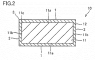
- a surface-coated cutting tool 10 has a rake face 1, a flank face 2, and a cutting edge ridgeline portion 3 at which rake face 1 and flank face 2 intersect with each other.
- rake face 1 and flank face 2 are surfaces connected to each other with cutting edge ridgeline portion 3 being interposed.
- Cutting edge ridgeline portion 3 implements a cutting edge tip end portion of tool 10.
- Such a shape of tool 10 relies on a shape of a base material which will be described later.
- Fig. 1 shows tool 10 representing a throwaway chip for turning
- tool 10 is not limited thereto and the tool can suitably be used as a cutting tool such as a drill, an end mill, a throwaway tip for a drill, a throwaway tip for an end mill, a throwaway tip for milling, a metal saw, a gear cutting tool, a reamer, and a tap.
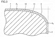
- tool 10 When tool 10 is implemented as a throwaway chip, tool 10 may or may not have a chip breaker, and cutting edge ridgeline portion 3 may have a sharp edge (a ridge at which a rake face and a flank face intersect with each other) (see Fig 1 ), may be honed (a sharp edge provided with R) (see Fig. 3 ), may have a negative land (beveled), and may be honed and have a negative land.
- a sharp edge a ridge at which a rake face and a flank face intersect with each other
- R sharp edge provided with R
- Fig. 3 may have a negative land (beveled), and may be honed and have a negative land.
- tool 10 has a base material 11 and a coating 12 formed on base material 11.
- coating 12 preferably covers the entire surface of base material 11 in tool 10, a part of base material 11 being not covered with coating 12 or a partially different construction of coating 12 does not depart from the scope of the present embodiment.
- Base material 11 has a rake face 11a, a flank face 11b, and a cutting edge ridgeline portion 11c at which rake face 11a and flank face 11b intersect with each other.
- Rake face 11a, flank face 11b, and cutting edge ridgeline portion 11c implement rake face 1, flank face 2, and cutting edge ridgeline portion 3 of tool 10, respectively.
- any conventionally known base material of such a kind can be employed.
- a base material is preferably exemplified by cemented carbide (for example, WC-based cemented carbide, which contains not only WC but also Co, or to which a carbonitride of Ti, Ta, or Nb may be added), cermet (mainly composed of TiC, TiN, or TiCN), high-speed steel, ceramics (titanium carbide, silicon carbide, silicon nitride, aluminum nitride, or aluminum oxide), a cubic boron nitride sintered object, or a diamond sintered object.
- cemented carbide for example, WC-based cemented carbide, which contains not only WC but also Co, or to which a carbonitride of Ti, Ta, or Nb may be added
- cermet mainly composed of TiC, TiN, or TiCN
- high-speed steel high-speed steel
- ceramics titanium carbide, silicon carbide, silicon nitride, aluminum nit
- WC-based cemented carbide or cermet in particular, TiCN-based cermet
- TiCN-based cermet is preferably selected. This is because such base materials are particularly excellent in balance between hardness and strength at a high temperature and have characteristics excellent as a base material for the surface-coated cutting tool in applications above
- Coating 12 may include other layers so long as it includes an ⁇ -Al 2 O 3 layer.
- other layers can include a TiN layer, a TiCN layer, a TiBNO layer, a TiCNO layer, a TiB 2 layer, a TiAlN layer, a TiAlCN layer, a TiAlON layer, and a TiAlONC layer.
- An order of layering is not particularly limited.
- a chemical formula such as "TiN”, “TiCN,” or “TiC x N y " in which an atomic ratio is not particularly specified in the present embodiment does not indicate that an atomic ratio of each element is limited only to "1" but encompasses all conventionally known atomic ratios.
- Such a coating 12 according to the present embodiment has a function to improve various characteristics such as resistance to wear and resistance to chipping by covering base material 11.
- Coating 12 has a thickness suitably of 3-30 ⁇ m (not smaller than 3 ⁇ m and not greater than 30 ⁇ m, a numerical range expressed with "-" in the present application refers to a range including upper limit and lower limit numeric values) and more preferably of 5-20 ⁇ m
- a thickness is smaller than 3 ⁇ m, resistance to wear may be insufficient, and when the thickness exceeds 30 ⁇ m, peel-off or destruction of coating 12 may occur with high frequency during intermittent working, with application of a large stress between coating 12 and base material 11.
- Coating 12 includes an ⁇ -Al 2 O 3 layer.
- Coating 12 can include one ⁇ -Al 2 O 3 layer or two or more ⁇ -Al 2 O 3 layers.
- the ⁇ -Al 2 O 3 layer contains a plurality of crystal grains of ⁇ -Al 2 O 3 (aluminum oxide of which crystal structure is of an ⁇ type). Namely, this layer is composed of polycrystalline ⁇ -Al 2 O 3 . Normally, these crystal grains have a grain size approximately from 100 to 2000 nm. A "crystal grain boundary" is present between a plurality of crystal grains of ⁇ -Al 2 O 3 .
- the crystal grain boundary significantly affects characteristics of a substance such as growth of crystal grains, creep characteristics, diffusion characteristics, electric characteristics, optical characteristics, and mechanical characteristics.
- Important characteristics to be taken into consideration include, for example, a density of crystal grain boundaries in a substance, a chemical composition of an interface, and a crystallographic texture, that is, a crystal grain boundary plane orientation and crystal misorientation.
- a coincidence site lattice (CSL) crystal grain boundary plays a special role.
- the CSL crystal grain boundary (also simply referred to as a "CSL grain boundary”) is characterized by a multiplicity index ⁇ , and is defined as a ratio between a density of sites of crystal lattices of two crystal grains in contact with each other at the crystal grain boundary and a density of sites which coincide with each other when the crystal lattices are superimposed on each other. It has generally been admitted that, in a simple structure, a crystal grain boundary having a low ⁇ value tends to have low interface energy and special characteristics Therefore, control of a ratio of a special crystal grain boundary and a crystal misorientation distribution estimated from a CSL model is considered as important for characteristics of a ceramic coating and a method of improving those characteristics.
- EBSD electron beam backscattered diffraction
- a crystallographic orientation of each crystal grain of a substance of interest is determined after indexing of a corresponding diffraction pattern.
- a texture is analyzed and a grain boundary character distribution (GBCD) is determined relatively easily with EBSD, with the use of commercially available software
- GBCD grain boundary character distribution
- Crystal grain boundary misorientation of a sample population having a large interface can be determined by applying EBSD to the interfaces.
- Misorientation distribution is normally associated with a condition for treatment of a substance.
- Crystal grain boundary misorientation can be obtained based on a common orientation parameter such as an Euler angle, an angle/axis pair, or a Rodrigues' vector.
- the CSL model is widely used as a tool for determining characteristics.
- the crystal grain boundary in the ⁇ -Al 2 O 3 layer according to the present embodiment includes the CSL grain boundary and the general grain boundary described above.
- the CSL grain boundary is constituted of the ⁇ 3 crystal grain boundary, the ⁇ 7 crystal grain boundary, the ⁇ 11 crystal grain boundary, the ⁇ 17 crystal grain boundary, the ⁇ 19 crystal grain boundary, the ⁇ 21 crystal grain boundary, the ⁇ 23 crystal grain boundary, and the ⁇ 29 crystal grain boundary. Even when any one or more crystal grain boundaries other than the ⁇ 3 crystal grain boundary are not observed in observation with EBSD, such a case does not depart from the scope of the present embodiment so long as an effect of the present embodiment is exhibited.
- the general grain boundary refers to crystal grain boundaries other than the CSL crystal grain boundary. Therefore, the general grain boundary refers to a remainder resulting from exclusion of the CSL grain boundary from all grain boundaries of crystal grains of ⁇ -Al 2 O 3 in observation with EBSD
- the ⁇ -Al 2 O 3 layer according to the present embodiment satisfies (1) to (4) below.
- All areas of the ⁇ -Al 2 O 3 layer in a direction of thickness are subjected to color mapping of the ⁇ -Al 2 O 3 layer. Namely, all regions from the surface located on a cover surface side of the ⁇ -Al 2 O 3 layer to the surface located on a side of the base material of the ⁇ -Al 2 O 3 layer is subjected to color mapping. All areas in the direction of thickness of the ⁇ -Al 2 O 3 layer having a thickness of the order of micrometer can be observed in one observation image. On the other hand, any area in an in-plane direction (a direction orthogonal to the direction of thickness) of the ⁇ -Al 2 O 3 layer should only be subjected to color mapping.
- ⁇ -Al 2 O 3 layer is highly oriented in line with the (001) plane, a hardness of the ⁇ -Al 2 O 3 layer is higher. Therefore, according to the ⁇ -Al 2 O 3 layer in the present embodiment which satisfies (1), occurrence of a crack due to impact applied during working can be suppressed, toughness of the cutting tool can significantly be improved, and hence high resistance to wear can be achieved.
- the “surface side of the coating” means a side opposite to the side of the base material in the direction of thickness of the ⁇ -Al 2 O 3 layer, and when no other layer is formed on the ⁇ -Al 2 O 3 layer, it means the surface of the ⁇ -Al 2 O 3 layer.
- the all CSL crystal grain boundaries are denoted as the ⁇ 3-29 crystal grain boundary
- length L R3 of the ⁇ 3 crystal grain boundary in the ⁇ -Al 2 O 3 layer on the rake face side is defined as exceeding 80% of length L R3 - 39 of the ⁇ 3-29 crystal grain boundary in the ⁇ -Al 2 O 3 layer on the rake face side
- length L F3 of the ⁇ 3 crystal grain boundary in the ⁇ -Al 2 O 3 layer on the flank face side is defined as exceeding 80% of length L F3-29 of the ⁇ 3-29 crystal grain boundary in the ⁇ -Al 2O3 layer on the flank face side.
- Length L R3 refers to a total length of the ⁇ 3 crystal grain boundary in a field of view observed in observation with an SEM with EBSD of the ⁇ -Al 2 O 3 layer on the rake face side
- length L R3-29 refers to the total sum of lengths of the ⁇ 3 crystal grain boundary, the ⁇ 7 crystal grain boundary, the ⁇ 11 crystal grain boundary, the ⁇ 17 crystal grain boundary, the ⁇ 19 crystal grain boundary, the ⁇ 21 crystal grain boundary, the ⁇ 23 crystal grain boundary, and the ⁇ 29 crystal grain boundary in a field of view observed in observation with an SEM with EBSD of the ⁇ -Al 2 O 3 layer on the rake face side.
- length L F3 refers to a total length of the ⁇ 3 crystal grain boundary in a field of view observed in observation with an SEM with EBSD of the ⁇ -Al 2 O 3 layer on the flank face side
- length L F3-29 refers to the total sum of lengths of the ⁇ 3 crystal grain boundary, the ⁇ 7 crystal grain boundary, the ⁇ 11 crystal grain boundary, the ⁇ 17 crystal grain boundary, the ⁇ 19 crystal grain boundary, the ⁇ 21 crystal grain boundary, the ⁇ 23 crystal grain boundary, and the ⁇ 29 crystal grain boundary in a field of view observed in observation with an SEM with EBSD of the ⁇ -Al 2 O 3 layer on the flank face side.
- Length L R3 is more preferably 83% or higher and further preferably 85% or higher of length L R3-29 , This is also applicable to length L F3 , and length L F3 is more preferably 83% or higher and further preferably 85% or higher of length L F3-29 .
- a numeric value is thus preferably as high as possible, and an upper limit thereof does not have to be defined. From a point of view of a thin film being polycrystalline, however, the upper limit is 99% or lower.
- the ⁇ 3 crystal grain boundary has high conformity as is clear also from the fact that it is low in grain boundary energy, two crystal grains of which grain boundary is defined by the ⁇ 3 crystal grain boundary exhibit a behavior similar to a behavior of a single crystal or twin crystals and tend to be coarser. As crystal grains are coarser, characteristics of a coating such as resistance to chipping lower and hence coarsening should be suppressed. Therefore, in the present embodiment, the suppression effect above is ensured by defining respective lengths L R3 and L F3 of the ⁇ 3 crystal grain boundary to be not lower than 10% and not higher than 50% of total lengths L R and L F of all grain boundaries in the ⁇ -Al 2 O 3 layer located on the sides of the rake face and the flank face.
- a more preferred range of lengths L R3 and L F3 of the ⁇ 3 crystal grain boundary is from 20 to 45 % and a further preferred range is from 30 to 40%.
- total length L R of all grain boundaries on the side of the rake face can be expressed as the "sum of length L R3-29 of the ⁇ 3-29 crystal grain boundary and length L RG of the general grain boundary” and “total length L F of all grain boundaries” on the side of the flank face can be expressed as the "sum of length L F3-29 of the ⁇ 3-29 crystal grain boundary and length L FG of the general grain boundary.” (4) above will be described.
- the ⁇ -Al 2 O 3 layer satisfying (4) is relatively high in ratio occupied by the ⁇ 3 crystal grain boundary in the CSL grain boundary in the ⁇ -Al 2 O 3 layer on the side of the rake face and relatively low in ratio of the ⁇ 3 crystal grain boundary in the CSL grain boundary in the ⁇ -Al 2 O 3 layer on the side of the flank face. Therefore, the ⁇ -Al 2 O 3 layer satisfying (2) and (3) and further satisfying (4) is particularly excellent in resistance to plastic deformation on the side of the flank face and can sufficiently suppress lowering in characteristics of the coating such as resistance to chipping attributed to too much ⁇ 3 crystal grain boundary on the side of the rake face.
- high-speed and low-feed cutting process In a cutting process under a high-speed condition and a low-feed condition (hereinafter also denoted as a "high-speed and low-feed cutting process"), thermal load on the side of the flank face is high and wear of the flank face tends to increase.
- the ⁇ -Al 2 O 3 layer satisfying (2) to (4) can withstand load applied to the side of the flank face, and hence long life can be maintained also in the high-speed and low-feed cutting process under severe cutting conditions in particular on the side of the flank face.
- a difference ⁇ (L R3 /L R3-29 )-(LF 3 /LF 3-29 ) ⁇ between ratio L R3 /L R3-29 and ratio L F3 /L F3-29 is preferably from -1 to -10. In this case, balance between improvement in resistance to chipping on the side of the rake face and improvement in resistance to plastic deformation on the side of the flank face is excellent The difference is more preferably from -4 to -9.
- length L R3 of the ⁇ 3 crystal grain boundary is preferably from 80 to 95%, more preferably from 83 to 95%, and particularly preferably from 80 to 90%, of length L R3-29 ) of the ⁇ 3-29 crystal grain boundary
- Length L F3 of the ⁇ 3 crystal grain boundary is preferably from 90 to 99% and more preferably from 91 to 99% of length L F3-29 of the ⁇ 3-29 crystal grain boundary.
- whether or not the ⁇ -Al 2 O 3 layer satisfies (1) can be determined as follows.
- an ⁇ -Al 2 O 3 layer is formed on the base material based on a manufacturing method which will be described later. Then, the formed ⁇ -Al 2 O 3 layer (including the base material) on the side of the rake face is cut to obtain a cross-section perpendicular to the ⁇ -Al 2 O 3 layer (that is, cut to expose a cut surface obtained by cutting the ⁇ -Al 2 O 3 layer along a plane including a normal line to the surface of the ⁇ -Al 2 O 3 layer). Thereafter, the cut surface is polished with water resistant sandpaper (which contains an SiC grain abrasive as an abrasive).
- water resistant sandpaper which contains an SiC grain abrasive as an abrasive
- the layer is cut, for example, in such a manner that the surface of the ⁇ -Al 2 O 3 layer (when another layer is formed on the ⁇ -Al 2 O 3 layer, a surface of the coating) is fixed with the use of wax or the like as being in intimate contact to a sufficiently large flat plate for holding, and thereafter the ⁇ -Al 2 O 3 layer is cut in a direction perpendicular to the flat plate with a cutter with a rotary blade (cut such that the rotary blade and the flat plate are as perpendicular as possible to each other). Any portion of the ⁇ -Al 2 O 3 layer can be cut so long as the ⁇ -Al 2 O 3 layer is cut in such a perpendicular direction.
- Polishing is performed successively with water resistant sandpaper #400, #800, and #1500 (the number (#) of the water resistant sandpaper means a difference in grain size of the abrasive, and a greater number indicates a smaller grain size of the abrasive).
- the polished surface is further smoothened through ion milling treatment with the use of Ar ions. Conditions for ion milling treatment are as follows.
- Irradiation angle 0° from a direction of normal to the surface of the ⁇ -Al 2 O 3 layer (that is, a linear direction in parallel to a direction of thickness of the ⁇ -Al 2 O 3 layer at the cut surface)
- a position of cutting is set to avoid at least a portion in the vicinity of cutting edge ridgeline portion 3.
- flank face 2 and flank face 2 are in contact with each other is regarded as cutting edge ridgeline portion 3, and a position distant by 0.2 mm or greater from outer edge A 1 which is an end portion of cutting edge ridgeline portion 3 (a position distant from outer edge A 1 to the left in Fig. 3 ) is applied as a position of a cross-section Similarly also in a cross-section on the side of flank face 2 of the ⁇ -Al 2 O 3 layer, a position distant by 0.2 mm or greater from outer edge A 2 which is an end portion of cutting edge ridgeline portion 3 (a position distant from outer edge A 2 in a downward direction in Fig. 3 ) is applied as a position of a cross-section.
- the smoothened polished surface is observed with an SEM with EBSD.
- Zeiss Supra 35 VP manufactured by CARL ZEISS
- HKL NL02 EBSD detector is employed as the SEM.
- EBSD data is successively collected by individually positioning focused electron beams onto each pixel.
- a normal line to a sample surface (a smoothened cross-section of the ⁇ -Al 2 O 3 layer) is inclined by 70° with respect to incident beams, and analysis is conducted at 15 kV. In order to avoid a charging effect, a pressure of 10 Pa is applied.
- a high current mode is set in conformity with a diameter of an opening of 60 ⁇ m or 120 ⁇ m. Data is collected stepwise at 0.1 ⁇ m/step, for 500 ⁇ 300 points corresponding to a plane region of 50 ⁇ 30 ⁇ m on the polished surface.
- an angle formed between a direction of normal to the (001) plane of each measured pixel and a direction of normal to the surface of the ⁇ -Al 2 O 3 layer (the surface located on the surface side of the coating) (that is, the linear direction in parallel to the direction of thickness of the ⁇ -Al 2 O 3 layer at the cut surface) is calculated, and a color map in which a pixel having the angle within ⁇ 20° is selected is created.
- the ⁇ -Al 2 O 3 layer on the side of the flank face shows (001) orientation.
- the ⁇ -Al 2 O 3 layer on the side of any surface shows (001) orientation, that is, a ratio of crystal grains ( ⁇ -Al 2 O 3 ) of which direction of normal to the (001) plane is within ⁇ 20° with respect to the direction of normal to the surface (the surface located on the surface side of the coating) of the ⁇ -Al 2 O 3 layer is not lower than 50%, the ⁇ -Al 2 O 3 layer satisfies (1).
- the ⁇ -Al 2 O 3 layer on the side of the rake face is cut to obtain a cross-section perpendicular to the ⁇ -Al 2 O 3 layer similarly to the above, and thereafter polishing and smoothing treatment are similarly carried out. Then, the cut surface thus treated is observed with an SEM with EBSD as above.
- a normal line to a sample surface (a smoothened cross-section of the ⁇ -Al 2 O 3 layer) is inclined by 70° with respect to incident beams, and analysis is conducted at 15 kV. In order to avoid a charging effect, a pressure of 10 Pa is applied.
- a high current mode is set in conformity with a diameter of an opening of 60 ⁇ m or 120 ⁇ m. Data is collected stepwise at 0.1 ⁇ m/step, for 500 ⁇ 300 points corresponding to a plane region of 50 ⁇ 30 ⁇ m on the polished surface.
- length L R3 of the ⁇ 3 crystal grain boundary, length L R3-29 of the ⁇ 3-29 crystal grain boundary, and total length L R of all grain boundaries in the ⁇ -Al 2 O 3 layer on the side of the rake face can be found.
- length L F3 of the ⁇ 3 crystal grain boundary, length L F3-29 of the ⁇ 3-29 crystal grain boundary, and total length L F of all grain boundaries in the ⁇ -Al 2 O 3 layer on the side of the flank face can be found.
- the layer preferably has a thickness from 2 to 20 ⁇ m.
- the excellent effect as above can thus be exhibited.
- the thickness is more preferably from 2 to 15 ⁇ m and further preferably from 2 to 10 ⁇ m.
- the thickness is smaller than 2 ⁇ m, the excellent effect as above may not sufficiently be exhibited.
- the thickness exceeds 20 ⁇ m, interface stress attributed to a difference in coefficient of linear expansion between the ⁇ -Al 2 O 3 layer and another layer such as an underlying layer increases and crystal grains of ⁇ -Al 2 O 3 may come off
- SEM scanning electron microscope
- the ⁇ -Al 2 O 3 layer has surface roughness Ra preferably less than 0.2 ⁇ m.
- Surface roughness Ra is more preferably less than 0.15 ⁇ m and further preferably less than 0.10 ⁇ m.
- Surface roughness Ra is thus preferably as low as possible, and a lower limit thereof does not have to be defined. From a point of view of the fact that a coating is affected by a surface texture of the base material, however, the lower limit is 0 05 ⁇ m or greater.
- surface roughness Ra means arithmetical mean roughness Ra defined under JIS B 0601 (2001).
- the ⁇ -Al 2 O 3 layer preferably includes a point where an absolute value for compressive stress is maximal, in a region within 2 ⁇ m from a surface side of the coating, and the absolute value for compressive stress at the point is lower than 1 GPa.
- the absolute value is more preferably lower than 0.9 GPa and further preferably lower than 0.8 GPa.
- the lower limit of the absolute value is not particularly limited, from a point of view of balance between resistance to wear and resistance to breakage, the lower limit is not lower than 0.2 GPa.
- Compressive stress in the present embodiment can be measured with the conventionally known sin 2 ⁇ method and constant penetration depth method which use X-rays.
- the coating according to the present embodiment can include a TiC x N y layer between the base material and the ⁇ -Al 2 O 3 layer.
- This TiC x N y layer preferably contains TiC x N y satisfying atomic ratio relation of 0.6 ⁇ x/(x+y) ⁇ 0.8. Adhesion between the base material and the ⁇ -Al 2 O 3 layer is thus improved.
- the atomic ratio is more preferably 0.65 ⁇ x/(x+y) ⁇ 0.75 and further preferably 0.67 ⁇ x/(x+y) ⁇ 0.72.
- x/(x+y) is smaller than 0.6, resistance to wear may be insufficient, and when it exceeds 0.8, resistance to chipping may be insufficient.
- the surface-coated cutting tool according to the present embodiment can be manufactured by forming a coating on a base material through chemical vapor deposition (CVD).
- CVD chemical vapor deposition
- a layer other than the ⁇ -Al 2 O 3 layer is formed in the coating, such a layer can be formed under conventionally known conditions with the use of a chemical vapor deposition apparatus.
- the ⁇ -Al 2 O 3 layer can be formed as below.
- AlCl 3 , HCl, CO 2 , H 2 S, O 2 , and H 2 are employed as source gases. Amounts of blend of AlCl 3 , HCl, CO 2 , H 2 S, and O 2 are set to 3 to 5 volume %, 4 to 6 volume %, 0.5 to 2 volume %, 1 to 5 volume %, and 0.0001 to 0,01 volume %, respectively, and H 2 is adopted as the remainder. Volume ratios of 0.1 ⁇ CO 2 /H 2 S ⁇ 1, 0.1 ⁇ CO 2 /AlCl 3 ⁇ 1, and 0.5 ⁇ AlCl 3 /HCl ⁇ 1 are adopted.
- a direction of injection of the source gas is adjusted such that the flank face of the base material is substantially perpendicular to the direction of injection of the source gas and the rake face of the base material is substantially in parallel to the direction of injection of the source gas.
- Various conditions for chemical vapor deposition include a temperature from 950 to 1050°C, a pressure from 1 to 5 kPa, and a gas flow rate (a total amount of gases) from 50 to 100 L/min.
- a speed of introduction of the source gas into the reaction vessel is set to 1.7 to 3.5 m/sec.
- annealing is performed.
- Conditions for annealing include a temperature from 1050 to 1080°C, a pressure from 50 to 100 kPa, and a time period from 120 to 300 minutes.
- An atmosphere for this annealing is obtained by feeding H 2 and argon (Ar) each at a flow rate of 20 to 30 L/min.
- the ⁇ -Al 2 O 3 layer according to the present embodiment having a desired thickness can thus be formed.
- the ⁇ -Al 2 O 3 layer satisfying (2) to (4) can be formed. The reason is estimated as follows.
- O 2 is more reactive than other gases such as CO 2 , and it has a function to increase the number of nuclei of ⁇ -Al 2 O 3 or to increase a rate of film formation.
- O 2 can also have a function to lower a ratio of the ⁇ 3 crystal grain boundary in the CSL crystal grain boundary. This is because generation of the ⁇ 3 crystal grain boundary which is the crystal grain boundary having high conformity is less likely when a rate of film formation is too high.
- a flux density of a source gas tends to relatively be high
- a flux density of a source gas tends to be relatively low
- a residence time of a source gas tends to be short on the side of the rake face
- a residence time of a source gas tends to be long on the side of the flank face.
- the side of the rake face tends to be supplied with a source gas more frequently than the side of the flank face.
- Annealing as above after film formation can prevent an impurity such as sulfur from remaining in the ⁇ -Al 2 O 3 layer. Therefore, the method of manufacturing the ⁇ -Al 2 O 3 layer according to the present embodiment is particularly excellent.
- a base material made of cemented carbide and having a shape of CNMG120408NUX manufactured by Sumitomo Electric Industries, Ltd.
- Table 1 Formulated Composition (Mass %) Co Ni TiN TiC Mo 2 C TaC WC P 5.0 - 0.5 0.5 - 2.0 Remainder K 4.0 6.0 15.0 Remainder 10.0 - Remainder
- a coating was formed on a surface of each base material obtained as above. Specifically, a coating was formed on the base material through chemical vapor deposition, with the base material being set in a chemical vapor deposition apparatus.
- the base material was arranged in the reaction vessel such that the rake face was substantially in parallel to a direction of injection of a gas and the flank face was substantially orthogonal to the direction of injection of the gas.
- Conditions for forming the coating are as shown in Tables 2 and 3 below.
- Table 2 shows conditions for forming each layer other than the ⁇ -Al 2 O 3 layer
- Table 3 shows conditions for forming the ⁇ -Al 2 O 3 layer.
- TiBNO and TiCNO in Table 2 represent an intermediate layer in Table 5 which will be described later, and other components correspond to layers except for the ⁇ -Al 2 O 3 layer in Table 5.
- the TiC x N y layer is composed of TiC x N y in which an atomic ratio x/(x+y) is set to 0.7.
- formation condition A indicates that the ⁇ -Al 2 O 3 layer is formed by supplying a source gas composed of 3.2 volume % of AlCl 3 , 4.0 volume % of HCl, 1.0 volume % of CO 2 , 2 volume % of H 2 S, 0.003 volume % of O 2 , and remainder H 2 to the chemical vapor deposition apparatus, performing chemical vapor deposition under conditions of a pressure of 3.5 kPa, a temperature of 1000°C, and a flow rate (a total amount of gases) of 70 L/min., and thereafter performing annealing for 180 minutes under the conditions above.
- a source gas composed of 3.2 volume % of AlCl 3 , 4.0 volume % of HCl, 1.0 volume % of CO 2 , 2 volume % of H 2 S, 0.003 volume % of O 2 , and remainder H 2
- the chemical vapor deposition apparatus performing chemical vapor deposition under conditions of a pressure of 3.5 kPa, a temperature of 1000°C,
- Each layer other than the ⁇ -Al 2 O 3 layer shown in Table 2 was formed similarly through chemical vapor deposition, except for not performing annealing.
- the "remainder” in Table 2 indicates that H 2 occupies the remainder of the source gases.
- the “total amount of gases” indicates a total volume flow rate introduced into the chemical vapor deposition apparatus per unit time, with a gas in a standard condition (0°C and 1 atmospheric pressure) being defined as the ideal gas (also applicable to the ⁇ -Al 2 O 3 layer in Table 3).
- a thickness of each layer was adjusted by adjusting as appropriate a time period for film formation (a rate of film formation of each layer was approximately from 0.5 to 2.0 ⁇ m/hour).
- Tables 4 and 5 a composition and a thickness of each coating were determined with an SEM-EDX (scanning electron microscope-energy dispersive X-ray spectrometry), and a length of the ⁇ 3 crystal grain boundary, a length of the ⁇ 3-29 crystal grain boundary, and a total length of all grain boundaries of the ⁇ -Al 2 O 3 layer were determined with the method described above.
- SEM-EDX scanning electron microscope-energy dispersive X-ray spectrometry
- a ratio (%) of crystal grains ( ⁇ -Al 2 O 3 ) of which normal direction to the (001) plane is within ⁇ 20° with respect to the normal direction to the surface of the ⁇ -Al 2 O 3 layer (the surface located on the surface side of the coating) in the ⁇ -Al 2 O 3 layers on the side of the rake face and on the side of the flank face was determined with the method described above.
- the surface-coated cutting tool in Example 1 has a coating having a total thickness of 24.3 ⁇ m formed on the base material, by adopting base material P shown in Table 1 as the base material, forming a TiN layer having a thickness of 1.2 ⁇ m as an underlying layer on the surface of base material P under the conditions in Table 2, forming a TiC x N y layer having a thickness of 13.0 ⁇ m on the underlying layer under the conditions in Table 2, forming a TiBNO layer having a thickness of 0.7 ⁇ m as an intermediate layer on the TiC x N y layer under the conditions in Table 2, fabricating the ⁇ -Al 2 O 3 layer having a thickness of 8.6 ⁇ m on the intermediate layer under the formation condition A in Table 3, and thereafter forming a TiN layer having a thickness of 0.9 ⁇ m as an outermost layer under the conditions in Table 2. Blank fields in Table 4 indicate absence of a corresponding layer.
- length L R3 of the ⁇ 3 crystal grain boundary is 89% of length L R3-29 of the ⁇ 3-29 crystal grain boundary and 17% of total length L R of all grain boundaries.
- length L F3 of the ⁇ 3 crystal grain boundary is 94% of length L F3-29 of the ⁇ 3-29 crystal grain boundary and 20% of total length L F of all grain boundaries.
- a value calculated by subtracting a ratio (L F3 /L F3-29 ) (%) from a ratio (L F3 /L F3-29 ) (%) is shown in a field of "(L R3 /L R3-29 )-(L F3 /L F3-29 )". Since this value is "-", it can be seen that ratio L R3 /L R3-29 is lower than ratio L F3 /L F3-29 .
- This ⁇ -Al 2 O 3 layer shows (001) orientation on the side of the rake face and on the side of the flank face.
- the cutting test below belongs to the high-speed and low-feed cutting process.
- the surface-coated cutting tools in Examples are better in both of resistance to wear and resistance to chipping and longer in life of the tool than the surface-coated cutting tools in Comparative Examples. Namely, it could be confirmed that mechanical characteristics of the coating in the surface-coated cutting tools in Examples were improved.
- the surface-coated cutting tools in Examples are better in resistance to breakage and longer in life of the tool than the surface-coated cutting tools in Comparative Examples. Namely, it could be confirmed that mechanical characteristics of the coating in the surface-coated cutting tools in Examples were improved.
- a time period of cutting until the tool is broken under conditions for cutting below was counted for the surface-coated cutting tools in Examples 1, 1B, 1C, 2, 2B, 2C, 11, and 11B.
- Table 9 shows results.
- a longer time period of cutting indicates suppression of breakage of the cutting edge of the tool due to mechanical and thermal fatigue which occurs during an intermittent cutting process and resultant improvement in reliability of the cutting edge.
Landscapes
- Chemical & Material Sciences (AREA)
- Engineering & Computer Science (AREA)
- Mechanical Engineering (AREA)
- Chemical Kinetics & Catalysis (AREA)
- Materials Engineering (AREA)
- Metallurgy (AREA)
- Organic Chemistry (AREA)
- Inorganic Chemistry (AREA)
- General Chemical & Material Sciences (AREA)
- Ceramic Engineering (AREA)
- Cutting Tools, Boring Holders, And Turrets (AREA)
- Chemical Vapour Deposition (AREA)
- Drilling Tools (AREA)
- Gear Processing (AREA)
- Milling, Broaching, Filing, Reaming, And Others (AREA)
Claims (7)
- Oberflächenbeschichtetes Schneidwerkzeug mit einer Spanfläche und einer Flankenfläche, umfassend:ein Basismaterial; undeine auf dem Basismaterial gebildete Beschichtung,wobei die Beschichtung eine α-Al2O3-Schicht umfasst,wobei die α-Al2O3-Schicht eine Vielzahl von Kristallkörnern aus α-Al2O3 enthält,wobei eine Korngrenze der Kristallkörner eine CSL-Korngrenze und eine allgemeine Korngrenze umfasst,wobei die α-Al2O3-Schicht auf einer Spanflächenseite eine (001)- Ausrichtung aufweist,wobei in der α-Al2O3-Schicht auf der Spanflächenseite eine Länge LR3 einer Σ3 Kristallkorngrenze in der CSL-Korngrenze 80% einer Länge LR3-29 einer Σ3-29 Kristallkorngrenze überschreitet und nicht niedriger als 10% und nicht höher als 50% einer Gesamtlänge LR aller Korngrenzen ist, die eine Summe aus der Länge LR3-29 und einer Länge LRG der allgemeinen Korngrenze ist,wobei die α-Al2O3-Schicht auf einer Flankenflächenseite eine (001)-Ausrichtung aufweist,wobei in der α-Al2O3-Schicht auf der Flankenseitenseite eine Länge LF3 einer Σ3 Kristallkorngrenze in der CSL-Korngrenze 80% einer Länge LF3-29 einer Σ3-29 Kristallkorngrenze überschreitet und nicht niedriger als 10% und nicht höher als 50% einer Gesamtlänge LF aller Korngrenzen ist, die eine Summe aus der Länge LF3-29 und einer Länge LFG der allgemeinen Korngrenze ist, undein Verhältnis LR3/LR3-29 der Länge LR3 zur Länge LR3-29 niedriger als ein Verhältnis LF3/LF3-29 der Länge LF3 zur Länge LF3-29 ist.
- Oberflächenbeschichtetes Schneidwerkzeug nach Anspruch 1, wobei
die CSL-Korngrenze aus der Σ3 Kristallkorngrenze, einer Σ7 Kristallkorngrenze, einer Σ11 Kristallkorngrenze, einer Σ17 Kristallkorngrenze, einer Σ19 Kristallkorngrenze, einer Σ21 Kristallkorngrenze, einer Σ23 Kristallkorngrenze und einer Σ29 Kristallkorngrenze gebildet ist,
die Länge LR3-29 eine Gesamtsumme der Längen der Σ3 Kristallkorngrenze, der Σ7 Kristallkorngrenze, der Σ11 Kristallkorngrenze, der Σ17 Kristallkorngrenze, der Σ19 Kristallkorngrenze, der Σ21 Kristallkorngrenze, der Σ23 Kristallkorngrenze und der Σ29 Kristallkorngrenze in der α-Al2O3-Schicht auf der Spanflächenseite ist, und
die Länge LF3-29 eine Gesamtsumme der Längen der Σ3 Kristallkorngrenze, der Σ7 Kristallkorngrenze, der Σ11 Kristallkorngrenze, der Σ17 Kristallkorngrenze, der Σ19 Kristallkorngrenze, der Σ21 Kristallkorngrenze, der Σ23 Kristallkorngrenze und der Σ29 Kristallkorngrenze in der α-Al2O3-Schicht auf der Flankenflächenseite ist. - Oberflächenbeschichtetes Schneidwerkzeug nach Anspruch 1 oder 2, wobei die α-Al2O3-Schicht eine Dicke von 2 bis 20 µm aufweist.
- Oberflächenbeschichtetes Schneidwerkzeug nach einem der Ansprüche 1 bis 3, wobei die α-Al2O3-Schicht eine Oberflächenrauheit Ra von weniger als 0,2 µm aufweist.
- Oberflächenbeschichtetes Schneidwerkzeug nach einem der Ansprüche 1 bis 4, wobei die α-Al2O3-Schicht einen Punkt umfasst, an dem in einem Bereich innerhalb von 2 µm von einer Oberflächenseite der Beschichtung ein Absolutwert für die Druckspannung maximal ist, und der Absolutwert für die Druckspannung an dem Punkt niedriger als 1 GPa ist.
- Oberflächenbeschichtetes Schneidwerkzeug nach einem der Ansprüche 1 bis 5, wobei die Beschichtung eine TiCxNy-Schicht zwischen dem Basismaterial und der α-Al2O3-Schicht umfasst, und
die TiCxNy-Schicht TiCxNy enthält, das eine Atomverhältnisbeziehung von 0,6 ≤ x/(x+y) ≤ 0,8 erfüllt. - Oberflächenbeschichtetes Schneidwerkzeug nach einem der Ansprüche 1 bis 6, wobei die (001)-Ausrichtung als eine solche Bedingung definiert ist, dass ein Verhältnis der Kristallkörner aus α-Al2O3, deren Normalrichtung zu einer (001)-Ebene innerhalb von ±20° in Bezug auf eine Normalrichtung zu einer Oberfläche der α-Al2O3-Schicht liegt, nicht niedriger als 50% in der α-Al2O3-Schicht ist.
Applications Claiming Priority (1)
| Application Number | Priority Date | Filing Date | Title |
|---|---|---|---|
| PCT/JP2015/070030 WO2017009929A1 (ja) | 2015-07-13 | 2015-07-13 | 表面被覆切削工具 |
Publications (3)
| Publication Number | Publication Date |
|---|---|
| EP3323539A1 EP3323539A1 (de) | 2018-05-23 |
| EP3323539A4 EP3323539A4 (de) | 2018-06-27 |
| EP3323539B1 true EP3323539B1 (de) | 2019-03-20 |
Family
ID=55362138
Family Applications (1)
| Application Number | Title | Priority Date | Filing Date |
|---|---|---|---|
| EP15882291.6A Active EP3323539B1 (de) | 2015-07-13 | 2015-07-13 | Oberflächenbeschichtetes schneidwerkzeug |
Country Status (6)
| Country | Link |
|---|---|
| US (1) | US9878373B2 (de) |
| EP (1) | EP3323539B1 (de) |
| JP (1) | JP5871354B1 (de) |
| KR (1) | KR102126103B1 (de) |
| CN (1) | CN106536100B (de) |
| WO (1) | WO2017009929A1 (de) |
Families Citing this family (7)
| Publication number | Priority date | Publication date | Assignee | Title |
|---|---|---|---|---|
| EP3106250B1 (de) * | 2014-03-25 | 2019-07-24 | Kanefusa Kabushiki Kaisha | Schneidwerkzeug |
| CN110100046B (zh) * | 2017-01-26 | 2021-10-01 | 瓦尔特公开股份有限公司 | 涂层切削工具 |
| US11167355B2 (en) * | 2018-10-15 | 2021-11-09 | Sumitomo Electric Hardmetal Corp. | Cutting tool |
| JP7167966B2 (ja) * | 2020-07-08 | 2022-11-09 | 株式会社タンガロイ | 被覆切削工具 |
| JP7167965B2 (ja) * | 2020-07-08 | 2022-11-09 | 株式会社タンガロイ | 被覆切削工具 |
| JP7302617B2 (ja) * | 2021-02-26 | 2023-07-04 | 株式会社タンガロイ | 被覆切削工具 |
| US12497689B2 (en) | 2021-08-30 | 2025-12-16 | Kennametal Inc. | Surface coated cutting tools |
Family Cites Families (17)
| Publication number | Priority date | Publication date | Assignee | Title |
|---|---|---|---|---|
| JPS5642412A (en) * | 1979-09-14 | 1981-04-20 | Yokogawa Hokushin Electric Corp | Automatic gain control circuit |
| JP2004122264A (ja) | 2002-09-30 | 2004-04-22 | Sumitomo Electric Ind Ltd | 被覆切削工具 |
| JP4518260B2 (ja) | 2005-01-21 | 2010-08-04 | 三菱マテリアル株式会社 | 硬質被覆層が高速断続切削加工ですぐれた耐チッピング性を発揮する表面被覆サーメット製切削工具 |
| JP4716252B2 (ja) * | 2005-05-24 | 2011-07-06 | 三菱マテリアル株式会社 | 厚膜化α型酸化アルミニウム層がすぐれた耐チッピング性を発揮する表面被覆サーメット製切削工具 |
| EP1788124B1 (de) * | 2005-11-18 | 2008-09-24 | Mitsubishi Materials Corporation | Hartstoffbeschichtetes Cermet-Schneidwerkzeug mit modifizierter alpha-Al2O3 Schicht |
| JP2007136631A (ja) * | 2005-11-21 | 2007-06-07 | Sumitomo Electric Hardmetal Corp | 刃先交換型切削チップ |
| US7597511B2 (en) * | 2007-12-28 | 2009-10-06 | Mitsubishi Materials Corporation | Surface-coated cutting tool with hard coating layer having excellent abrasion resistance |
| WO2009133814A1 (ja) * | 2008-04-30 | 2009-11-05 | 住友電気工業株式会社 | 表面被覆切削工具 |
| US8828527B2 (en) | 2009-03-18 | 2014-09-09 | Mitsubishi Materials Corporation | Surface-coated cutting tool |
| JP5440311B2 (ja) * | 2010-03-25 | 2014-03-12 | 三菱マテリアル株式会社 | 硬質被覆層がすぐれた耐剥離性と耐摩耗性を発揮する表面被覆切削工具 |
| ES2728705T3 (es) | 2011-09-16 | 2019-10-28 | Walter Ag | Herramienta de corte recubierta con alfa-alúmina diseñada con límites de grano |
| JP5831707B2 (ja) * | 2012-03-14 | 2015-12-09 | 三菱マテリアル株式会社 | 硬質被覆層が高速断続切削ですぐれた耐チッピング性を発揮する表面被覆切削工具 |
| KR20140001694A (ko) * | 2012-06-28 | 2014-01-07 | 대구텍 유한회사 | 절삭 인서트 |
| JP5935562B2 (ja) * | 2012-07-13 | 2016-06-15 | 三菱マテリアル株式会社 | 硬質被覆層がすぐれた初期なじみ性、耐チッピング性を発揮する表面被覆切削工具 |
| JP6198176B2 (ja) | 2013-02-26 | 2017-09-20 | 三菱マテリアル株式会社 | 表面被覆切削工具 |
| JP6150109B2 (ja) * | 2013-04-18 | 2017-06-21 | 三菱マテリアル株式会社 | 硬質被覆層がすぐれた耐チッピング性を発揮する表面被覆切削工具 |
| JP6233575B2 (ja) * | 2013-11-22 | 2017-11-22 | 三菱マテリアル株式会社 | 高速断続切削加工で硬質被覆層がすぐれた耐チッピング性を発揮する表面被覆切削工具 |
-
2015
- 2015-07-13 EP EP15882291.6A patent/EP3323539B1/de active Active
- 2015-07-13 CN CN201580003729.7A patent/CN106536100B/zh active Active
- 2015-07-13 WO PCT/JP2015/070030 patent/WO2017009929A1/ja not_active Ceased
- 2015-07-13 JP JP2015548515A patent/JP5871354B1/ja active Active
- 2015-07-13 US US15/100,008 patent/US9878373B2/en active Active
- 2015-07-13 KR KR1020167016205A patent/KR102126103B1/ko active Active
Non-Patent Citations (1)
| Title |
|---|
| None * |
Also Published As
| Publication number | Publication date |
|---|---|
| EP3323539A1 (de) | 2018-05-23 |
| KR20180025779A (ko) | 2018-03-09 |
| US20170189967A1 (en) | 2017-07-06 |
| US9878373B2 (en) | 2018-01-30 |
| EP3323539A4 (de) | 2018-06-27 |
| CN106536100B (zh) | 2019-06-14 |
| KR102126103B1 (ko) | 2020-06-23 |
| JPWO2017009929A1 (ja) | 2017-07-13 |
| WO2017009929A1 (ja) | 2017-01-19 |
| JP5871354B1 (ja) | 2016-03-01 |
| CN106536100A (zh) | 2017-03-22 |
Similar Documents
| Publication | Publication Date | Title |
|---|---|---|
| EP3323538B1 (de) | Oberflächenbeschichtetes schneidwerkzeug | |
| EP3296044B1 (de) | Oberflächenbeschichtetes schneidwerkzeug | |
| EP3323539B1 (de) | Oberflächenbeschichtetes schneidwerkzeug | |
| EP3311940B1 (de) | Oberflächenbeschichtetes schneidwerkzeug | |
| EP3323537B1 (de) | Oberflächenbeschichtetes schneidwerkzeug | |
| EP3936639A1 (de) | Beschichtetes schneidwerkzeug | |
| JP6439200B2 (ja) | 表面被覆切削工具の製造方法 | |
| EP3936638A1 (de) | Beschichtetes schneidwerkzeug | |
| JP6535922B2 (ja) | 表面被覆切削工具の製造方法 | |
| JP6439201B2 (ja) | 表面被覆切削工具の製造方法 |
Legal Events
| Date | Code | Title | Description |
|---|---|---|---|
| STAA | Information on the status of an ep patent application or granted ep patent |
Free format text: STATUS: THE INTERNATIONAL PUBLICATION HAS BEEN MADE |
|
| PUAI | Public reference made under article 153(3) epc to a published international application that has entered the european phase |
Free format text: ORIGINAL CODE: 0009012 |
|
| STAA | Information on the status of an ep patent application or granted ep patent |
Free format text: STATUS: REQUEST FOR EXAMINATION WAS MADE |
|
| 17P | Request for examination filed |
Effective date: 20180126 |
|
| AK | Designated contracting states |
Kind code of ref document: A1 Designated state(s): AL AT BE BG CH CY CZ DE DK EE ES FI FR GB GR HR HU IE IS IT LI LT LU LV MC MK MT NL NO PL PT RO RS SE SI SK SM TR |
|
| AX | Request for extension of the european patent |
Extension state: BA ME |
|
| A4 | Supplementary search report drawn up and despatched |
Effective date: 20180530 |
|
| RIC1 | Information provided on ipc code assigned before grant |
Ipc: C23C 16/56 20060101ALI20180524BHEP Ipc: C23C 16/40 20060101ALI20180524BHEP Ipc: C23C 28/04 20060101AFI20180524BHEP Ipc: C23C 16/36 20060101ALI20180524BHEP |
|
| REG | Reference to a national code |
Ref country code: DE Ref legal event code: R079 Ref document number: 602015026962 Country of ref document: DE Free format text: PREVIOUS MAIN CLASS: B23B0027140000 Ipc: C23C0028040000 |
|
| DAV | Request for validation of the european patent (deleted) | ||
| DAX | Request for extension of the european patent (deleted) | ||
| GRAP | Despatch of communication of intention to grant a patent |
Free format text: ORIGINAL CODE: EPIDOSNIGR1 |
|
| STAA | Information on the status of an ep patent application or granted ep patent |
Free format text: STATUS: GRANT OF PATENT IS INTENDED |
|
| RIC1 | Information provided on ipc code assigned before grant |
Ipc: C23C 16/36 20060101ALI20180925BHEP Ipc: C23C 28/04 20060101AFI20180925BHEP Ipc: C23C 16/56 20060101ALI20180925BHEP Ipc: C23C 16/40 20060101ALI20180925BHEP |
|
| INTG | Intention to grant announced |
Effective date: 20181019 |
|
| GRAS | Grant fee paid |
Free format text: ORIGINAL CODE: EPIDOSNIGR3 |
|
| GRAA | (expected) grant |
Free format text: ORIGINAL CODE: 0009210 |
|
| STAA | Information on the status of an ep patent application or granted ep patent |
Free format text: STATUS: THE PATENT HAS BEEN GRANTED |
|
| AK | Designated contracting states |
Kind code of ref document: B1 Designated state(s): AL AT BE BG CH CY CZ DE DK EE ES FI FR GB GR HR HU IE IS IT LI LT LU LV MC MK MT NL NO PL PT RO RS SE SI SK SM TR |
|
| REG | Reference to a national code |
Ref country code: GB Ref legal event code: FG4D |
|
| REG | Reference to a national code |
Ref country code: CH Ref legal event code: EP |
|
| REG | Reference to a national code |
Ref country code: DE Ref legal event code: R096 Ref document number: 602015026962 Country of ref document: DE |
|
| REG | Reference to a national code |
Ref country code: AT Ref legal event code: REF Ref document number: 1110619 Country of ref document: AT Kind code of ref document: T Effective date: 20190415 |
|
| REG | Reference to a national code |
Ref country code: IE Ref legal event code: FG4D |
|
| REG | Reference to a national code |
Ref country code: SE Ref legal event code: TRGR |
|
| REG | Reference to a national code |
Ref country code: NL Ref legal event code: MP Effective date: 20190320 |
|
| PG25 | Lapsed in a contracting state [announced via postgrant information from national office to epo] |
Ref country code: LT Free format text: LAPSE BECAUSE OF FAILURE TO SUBMIT A TRANSLATION OF THE DESCRIPTION OR TO PAY THE FEE WITHIN THE PRESCRIBED TIME-LIMIT Effective date: 20190320 Ref country code: NO Free format text: LAPSE BECAUSE OF FAILURE TO SUBMIT A TRANSLATION OF THE DESCRIPTION OR TO PAY THE FEE WITHIN THE PRESCRIBED TIME-LIMIT Effective date: 20190620 Ref country code: FI Free format text: LAPSE BECAUSE OF FAILURE TO SUBMIT A TRANSLATION OF THE DESCRIPTION OR TO PAY THE FEE WITHIN THE PRESCRIBED TIME-LIMIT Effective date: 20190320 |
|
| REG | Reference to a national code |
Ref country code: LT Ref legal event code: MG4D |
|
| PG25 | Lapsed in a contracting state [announced via postgrant information from national office to epo] |
Ref country code: BG Free format text: LAPSE BECAUSE OF FAILURE TO SUBMIT A TRANSLATION OF THE DESCRIPTION OR TO PAY THE FEE WITHIN THE PRESCRIBED TIME-LIMIT Effective date: 20190620 Ref country code: NL Free format text: LAPSE BECAUSE OF FAILURE TO SUBMIT A TRANSLATION OF THE DESCRIPTION OR TO PAY THE FEE WITHIN THE PRESCRIBED TIME-LIMIT Effective date: 20190320 Ref country code: LV Free format text: LAPSE BECAUSE OF FAILURE TO SUBMIT A TRANSLATION OF THE DESCRIPTION OR TO PAY THE FEE WITHIN THE PRESCRIBED TIME-LIMIT Effective date: 20190320 Ref country code: RS Free format text: LAPSE BECAUSE OF FAILURE TO SUBMIT A TRANSLATION OF THE DESCRIPTION OR TO PAY THE FEE WITHIN THE PRESCRIBED TIME-LIMIT Effective date: 20190320 Ref country code: GR Free format text: LAPSE BECAUSE OF FAILURE TO SUBMIT A TRANSLATION OF THE DESCRIPTION OR TO PAY THE FEE WITHIN THE PRESCRIBED TIME-LIMIT Effective date: 20190621 Ref country code: HR Free format text: LAPSE BECAUSE OF FAILURE TO SUBMIT A TRANSLATION OF THE DESCRIPTION OR TO PAY THE FEE WITHIN THE PRESCRIBED TIME-LIMIT Effective date: 20190320 |
|
| REG | Reference to a national code |
Ref country code: AT Ref legal event code: MK05 Ref document number: 1110619 Country of ref document: AT Kind code of ref document: T Effective date: 20190320 |
|
| PG25 | Lapsed in a contracting state [announced via postgrant information from national office to epo] |
Ref country code: IT Free format text: LAPSE BECAUSE OF FAILURE TO SUBMIT A TRANSLATION OF THE DESCRIPTION OR TO PAY THE FEE WITHIN THE PRESCRIBED TIME-LIMIT Effective date: 20190320 Ref country code: PT Free format text: LAPSE BECAUSE OF FAILURE TO SUBMIT A TRANSLATION OF THE DESCRIPTION OR TO PAY THE FEE WITHIN THE PRESCRIBED TIME-LIMIT Effective date: 20190720 Ref country code: SK Free format text: LAPSE BECAUSE OF FAILURE TO SUBMIT A TRANSLATION OF THE DESCRIPTION OR TO PAY THE FEE WITHIN THE PRESCRIBED TIME-LIMIT Effective date: 20190320 Ref country code: AL Free format text: LAPSE BECAUSE OF FAILURE TO SUBMIT A TRANSLATION OF THE DESCRIPTION OR TO PAY THE FEE WITHIN THE PRESCRIBED TIME-LIMIT Effective date: 20190320 Ref country code: EE Free format text: LAPSE BECAUSE OF FAILURE TO SUBMIT A TRANSLATION OF THE DESCRIPTION OR TO PAY THE FEE WITHIN THE PRESCRIBED TIME-LIMIT Effective date: 20190320 Ref country code: ES Free format text: LAPSE BECAUSE OF FAILURE TO SUBMIT A TRANSLATION OF THE DESCRIPTION OR TO PAY THE FEE WITHIN THE PRESCRIBED TIME-LIMIT Effective date: 20190320 Ref country code: RO Free format text: LAPSE BECAUSE OF FAILURE TO SUBMIT A TRANSLATION OF THE DESCRIPTION OR TO PAY THE FEE WITHIN THE PRESCRIBED TIME-LIMIT Effective date: 20190320 Ref country code: CZ Free format text: LAPSE BECAUSE OF FAILURE TO SUBMIT A TRANSLATION OF THE DESCRIPTION OR TO PAY THE FEE WITHIN THE PRESCRIBED TIME-LIMIT Effective date: 20190320 |
|
| PG25 | Lapsed in a contracting state [announced via postgrant information from national office to epo] |
Ref country code: SM Free format text: LAPSE BECAUSE OF FAILURE TO SUBMIT A TRANSLATION OF THE DESCRIPTION OR TO PAY THE FEE WITHIN THE PRESCRIBED TIME-LIMIT Effective date: 20190320 Ref country code: PL Free format text: LAPSE BECAUSE OF FAILURE TO SUBMIT A TRANSLATION OF THE DESCRIPTION OR TO PAY THE FEE WITHIN THE PRESCRIBED TIME-LIMIT Effective date: 20190320 |
|
| PG25 | Lapsed in a contracting state [announced via postgrant information from national office to epo] |
Ref country code: IS Free format text: LAPSE BECAUSE OF FAILURE TO SUBMIT A TRANSLATION OF THE DESCRIPTION OR TO PAY THE FEE WITHIN THE PRESCRIBED TIME-LIMIT Effective date: 20190720 Ref country code: AT Free format text: LAPSE BECAUSE OF FAILURE TO SUBMIT A TRANSLATION OF THE DESCRIPTION OR TO PAY THE FEE WITHIN THE PRESCRIBED TIME-LIMIT Effective date: 20190320 |
|
| REG | Reference to a national code |
Ref country code: DE Ref legal event code: R097 Ref document number: 602015026962 Country of ref document: DE |
|
| PLBE | No opposition filed within time limit |
Free format text: ORIGINAL CODE: 0009261 |
|
| STAA | Information on the status of an ep patent application or granted ep patent |
Free format text: STATUS: NO OPPOSITION FILED WITHIN TIME LIMIT |
|
| PG25 | Lapsed in a contracting state [announced via postgrant information from national office to epo] |
Ref country code: DK Free format text: LAPSE BECAUSE OF FAILURE TO SUBMIT A TRANSLATION OF THE DESCRIPTION OR TO PAY THE FEE WITHIN THE PRESCRIBED TIME-LIMIT Effective date: 20190320 |
|
| 26N | No opposition filed |
Effective date: 20200102 |
|
| PG25 | Lapsed in a contracting state [announced via postgrant information from national office to epo] |
Ref country code: MC Free format text: LAPSE BECAUSE OF FAILURE TO SUBMIT A TRANSLATION OF THE DESCRIPTION OR TO PAY THE FEE WITHIN THE PRESCRIBED TIME-LIMIT Effective date: 20190320 |
|
| REG | Reference to a national code |
Ref country code: CH Ref legal event code: PL |
|
| GBPC | Gb: european patent ceased through non-payment of renewal fee |
Effective date: 20190713 |
|
| PG25 | Lapsed in a contracting state [announced via postgrant information from national office to epo] |
Ref country code: TR Free format text: LAPSE BECAUSE OF FAILURE TO SUBMIT A TRANSLATION OF THE DESCRIPTION OR TO PAY THE FEE WITHIN THE PRESCRIBED TIME-LIMIT Effective date: 20190320 |
|
| REG | Reference to a national code |
Ref country code: BE Ref legal event code: MM Effective date: 20190731 |
|
| PG25 | Lapsed in a contracting state [announced via postgrant information from national office to epo] |
Ref country code: GB Free format text: LAPSE BECAUSE OF NON-PAYMENT OF DUE FEES Effective date: 20190713 |
|
| PG25 | Lapsed in a contracting state [announced via postgrant information from national office to epo] |
Ref country code: LI Free format text: LAPSE BECAUSE OF NON-PAYMENT OF DUE FEES Effective date: 20190731 Ref country code: BE Free format text: LAPSE BECAUSE OF NON-PAYMENT OF DUE FEES Effective date: 20190731 Ref country code: CH Free format text: LAPSE BECAUSE OF NON-PAYMENT OF DUE FEES Effective date: 20190731 Ref country code: LU Free format text: LAPSE BECAUSE OF NON-PAYMENT OF DUE FEES Effective date: 20190713 |
|
| PG25 | Lapsed in a contracting state [announced via postgrant information from national office to epo] |
Ref country code: FR Free format text: LAPSE BECAUSE OF NON-PAYMENT OF DUE FEES Effective date: 20190731 |
|
| PG25 | Lapsed in a contracting state [announced via postgrant information from national office to epo] |
Ref country code: IE Free format text: LAPSE BECAUSE OF NON-PAYMENT OF DUE FEES Effective date: 20190713 |
|
| PG25 | Lapsed in a contracting state [announced via postgrant information from national office to epo] |
Ref country code: CY Free format text: LAPSE BECAUSE OF FAILURE TO SUBMIT A TRANSLATION OF THE DESCRIPTION OR TO PAY THE FEE WITHIN THE PRESCRIBED TIME-LIMIT Effective date: 20190320 |
|
| PG25 | Lapsed in a contracting state [announced via postgrant information from national office to epo] |
Ref country code: MT Free format text: LAPSE BECAUSE OF FAILURE TO SUBMIT A TRANSLATION OF THE DESCRIPTION OR TO PAY THE FEE WITHIN THE PRESCRIBED TIME-LIMIT Effective date: 20190320 Ref country code: HU Free format text: LAPSE BECAUSE OF FAILURE TO SUBMIT A TRANSLATION OF THE DESCRIPTION OR TO PAY THE FEE WITHIN THE PRESCRIBED TIME-LIMIT; INVALID AB INITIO Effective date: 20150713 |
|
| PG25 | Lapsed in a contracting state [announced via postgrant information from national office to epo] |
Ref country code: SI Free format text: LAPSE BECAUSE OF FAILURE TO SUBMIT A TRANSLATION OF THE DESCRIPTION OR TO PAY THE FEE WITHIN THE PRESCRIBED TIME-LIMIT Effective date: 20190320 |
|
| PG25 | Lapsed in a contracting state [announced via postgrant information from national office to epo] |
Ref country code: MK Free format text: LAPSE BECAUSE OF FAILURE TO SUBMIT A TRANSLATION OF THE DESCRIPTION OR TO PAY THE FEE WITHIN THE PRESCRIBED TIME-LIMIT Effective date: 20190320 |
|
| P01 | Opt-out of the competence of the unified patent court (upc) registered |
Effective date: 20230515 |
|
| PGFP | Annual fee paid to national office [announced via postgrant information from national office to epo] |
Ref country code: SE Payment date: 20250528 Year of fee payment: 11 |
|
| PGFP | Annual fee paid to national office [announced via postgrant information from national office to epo] |
Ref country code: DE Payment date: 20250528 Year of fee payment: 11 |