EP3323158B1 - Magnetische tunnelübergänge - Google Patents
Magnetische tunnelübergänge Download PDFInfo
- Publication number
- EP3323158B1 EP3323158B1 EP16824930.8A EP16824930A EP3323158B1 EP 3323158 B1 EP3323158 B1 EP 3323158B1 EP 16824930 A EP16824930 A EP 16824930A EP 3323158 B1 EP3323158 B1 EP 3323158B1
- Authority
- EP
- European Patent Office
- Prior art keywords
- magnetic
- region
- iridium
- electrode
- cobalt
- Prior art date
- Legal status (The legal status is an assumption and is not a legal conclusion. Google has not performed a legal analysis and makes no representation as to the accuracy of the status listed.)
- Active
Links
Images
Classifications
-
- H—ELECTRICITY
- H10—SEMICONDUCTOR DEVICES; ELECTRIC SOLID-STATE DEVICES NOT OTHERWISE PROVIDED FOR
- H10N—ELECTRIC SOLID-STATE DEVICES NOT OTHERWISE PROVIDED FOR
- H10N50/00—Galvanomagnetic devices
- H10N50/80—Constructional details
- H10N50/85—Materials of the active region
-
- G—PHYSICS
- G11—INFORMATION STORAGE
- G11C—STATIC STORES
- G11C11/00—Digital stores characterised by the use of particular electric or magnetic storage elements; Storage elements therefor
- G11C11/02—Digital stores characterised by the use of particular electric or magnetic storage elements; Storage elements therefor using magnetic elements
- G11C11/16—Digital stores characterised by the use of particular electric or magnetic storage elements; Storage elements therefor using magnetic elements using elements in which the storage effect is based on magnetic spin effect
- G11C11/161—Digital stores characterised by the use of particular electric or magnetic storage elements; Storage elements therefor using magnetic elements using elements in which the storage effect is based on magnetic spin effect details concerning the memory cell structure, e.g. the layers of the ferromagnetic memory cell
-
- H—ELECTRICITY
- H10—SEMICONDUCTOR DEVICES; ELECTRIC SOLID-STATE DEVICES NOT OTHERWISE PROVIDED FOR
- H10B—ELECTRONIC MEMORY DEVICES
- H10B61/00—Magnetic memory devices, e.g. magnetoresistive RAM [MRAM] devices
-
- H—ELECTRICITY
- H10—SEMICONDUCTOR DEVICES; ELECTRIC SOLID-STATE DEVICES NOT OTHERWISE PROVIDED FOR
- H10N—ELECTRIC SOLID-STATE DEVICES NOT OTHERWISE PROVIDED FOR
- H10N50/00—Galvanomagnetic devices
- H10N50/01—Manufacture or treatment
-
- H—ELECTRICITY
- H10—SEMICONDUCTOR DEVICES; ELECTRIC SOLID-STATE DEVICES NOT OTHERWISE PROVIDED FOR
- H10N—ELECTRIC SOLID-STATE DEVICES NOT OTHERWISE PROVIDED FOR
- H10N50/00—Galvanomagnetic devices
- H10N50/10—Magnetoresistive devices
-
- H—ELECTRICITY
- H10—SEMICONDUCTOR DEVICES; ELECTRIC SOLID-STATE DEVICES NOT OTHERWISE PROVIDED FOR
- H10N—ELECTRIC SOLID-STATE DEVICES NOT OTHERWISE PROVIDED FOR
- H10N50/00—Galvanomagnetic devices
- H10N50/80—Constructional details
Definitions
- a magnetic tunnel junction is an integrated circuit component having two conductive magnetic electrodes separated by a thin non-magnetic tunnel insulator material (e.g., dielectric material).
- the insulator material is sufficiently thin such that electrons can tunnel from one magnetic electrode to the other through the insulator material under appropriate conditions.
- At least one of the magnetic electrodes can have its overall magnetization direction switched between two states at a normal operating write or erase current/voltage, and is commonly referred to as the "free” or “recording” electrode.
- the other magnetic electrode is commonly referred to as the “reference”, “fixed”, or “pinned” electrode, and whose overall magnetization direction will not switch upon application of the normal operating write or erase current/voltage.
- the reference electrode and the recording electrode are electrically coupled to respective conductive nodes.
- a magnetic tunnel junction can be programmed into one of at least two states, and those states can be sensed by measuring current flow through the magnetic tunnel junction. Since magnetic tunnel junctions can be "programmed" between two current-conducting states, they have been proposed for use in memory integrated circuitry. Additionally, magnetic tunnel junctions may be used in logic, sensors, oscillators or other circuitry apart from or in addition to memory.
- the overall magnetization direction of the recording electrode can be switched by a current-induced external magnetic field or by using a spin-polarized current to result in a spin-transfer torque (STT) effect.
- Charge carriers such as electrons
- An electric current is generally unpolarized (having about 50% "spin-up” and about 50% “spin-down” electrons).
- a spin-polarized current is one with significantly more electrons of either spin.
- spin angular momentum can be transferred to that material, thereby affecting its magnetization orientation. This can be used to excite oscillations or even flip (i.e., switch) the orientation/domain direction of the magnetic material if the spin-polarized current is of sufficient magnitude.
- An alloy or other mixture of Co and Fe is one common material proposed for use as a polarizer material and/or as at least part of the magnetic recording material of a recording electrode in a magnetic tunnel junction.
- a more specific example is Co x Fe y B z where x and y are each 10-80 and z is 0-50, and may be abbreviated as CoFe or CoFeB.
- MgO is a suitable material for the non-magnetic tunnel insulator.
- Tunnel insulator materials are often crystalline, and are desired to have a body-centered-cubic (bcc) 001 lattice.
- Tunnel insulator and polarizer materials may be deposited using any suitable methodology (e.g., physical vapor deposition).
- One technique usable to ultimately produce the bcc 001 lattice in both tunnel insulator and adjacent polarizer material includes initially forming cobalt-and-iron-containing material of the polarizer to be amorphous and upon which tunnel insulator material (e.g., MgO) is deposited. During and/or after the depositing, the cobalt-and-iron-containing material and the tunnel insulator may each achieve a uniform bcc 001 lattice structure.
- tunnel insulator material e.g., MgO
- Prior art document US2012/0068285 A1 (Kitagawa et al. ) relates to a magnetoresistive effect element including a first and a second magnetic layer and a non-magnetic layer between the first and second magnetic layers.
- Prior art document US2014/027869 A1 (Lee et al. ) relates to a perpendicular magnetic tunnel junction apparatus including a tunnel magnetoresistance enhancement buffer layer.
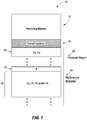
- FIGS. 1 and 2 are diagrammatic, cross-sectional views of example embodiment magnetic tunnel junctions
- Magnetic tunnel junctions may be utilized in spin-torque-transfer magnetic random access memory (STT-MRAM).
- STT-MRAM spin-torque-transfer magnetic random access memory
- an iridium-containing region is provided between a polarizer region and other magnetic regions of a reference material. The iridium-containing region may enable improved magnetic coupling of the polarizer region to the other magnetic regions, and may also enable perpendicular magnetic anisotropy along interfaces of iridium-containing material with the adjacent magnetic materials.
- the magnetic coupling through the iridium-containing region may be antiferromagnetic or ferromagnetic, depending on the thickness of the iridium-containing region. In some embodiments, the magnetic coupling through the iridium-containing region is stable to at least about 7 kilo-Oersteds (kOe, 1 Oe ⁇ 79.5775 A/m).
- a magnetic tunnel junction as defined in claim 1.
- a magnetic tunnel junction 10 comprises an electrically conductive first magnetic (i.e., ferrimagnetic or ferromagnetic) electrode 12 comprising magnetic recording material.
- An electrically conductive second magnetic electrode 14 is spaced from the first electrode 12 and comprises magnetic reference material. Accordingly, the first electrode 12 may function as a recording (i.e., free) electrode, and the second electrode 14 may function as a reference (i.e., pinned) electrode.
- a nonmagnetic tunnel insulator material 16 is between the first and second electrodes 12 and 14.
- any of the materials and/or structures described herein may be homogeneous or nonhomogeneous, and regardless may be continuous or discontinuous over any material which such overlie. Further, unless otherwise stated, each material may be formed using any suitable existing or yet-to-be-developed technique, with atomic layer deposition, chemical vapor deposition, physical vapor deposition, epitaxial growth, diffusion doping, and ion implanting being examples.
- the magnetic recording material and the magnetic reference material are individually overall and collectively magnetic, even though one or both may have one or more regions therein which are intrinsically nonmagnetic.
- the magnetic tunnel junction 10 may be supported by a semiconductor base (not shown).
- a semiconductor base may, for example, comprise semiconductor material, and in some embodiments may comprise, consist essentially of, or consist of monocrystalline silicon.
- the semiconductor base may be considered to be a semiconductor substrate.
- semiconductor substrate means any construction comprising semiconductive material, including, but not limited to, bulk semiconductive materials such as a semiconductive wafer (either alone or in assemblies comprising other materials), and semiconductive material layers (either alone or in assemblies comprising other materials).
- substrate refers to any supporting structure, including, but not limited to, the semiconductor substrates described above.
- the semiconductor substrate may contain one or more materials associated with integrated circuit fabrication. Some of the materials may correspond to, for example, one or more of refractory metal materials, barrier materials, diffusion materials, insulator materials, etc.
- first electrode 12 and second electrode 14 may be reversed.
- magnetic tunnel junction 10 is shown as being generally vertically or elevationally oriented in FIG. 1 , other orientations may be used. Such other orientations may include, for example, horizontal, diagonal, one or more combinations of horizontal, vertical, diagonal, etc.
- horizontal refers to a general direction along a primary surface relative to which the substrate is processed during fabrication, and “vertical” is a direction generally orthogonal thereto.
- vertical and “horizontal” as used herein are generally perpendicular directions relative one another independent of orientation of the substrate in three-dimensional space. Further in this document, “elevational”, “upper”, “lower”, “top”, and “bottom” are with reference to the vertical direction.
- example thicknesses for first electrode 12, tunnel insulator material 16, and second electrode 14 are about 5 to 200 Angstroms, about 5 to 50 Angstroms, and about 20 to 300 Angstroms, respectively.
- thickness by itself (no preceding directional adjective) is defined as the mean straight-line distance through a given material or region perpendicularly from a closest surface of an immediately adjacent material of different composition or of an immediately adjacent region.
- the various materials described herein may be of substantially constant thickness or of variable thicknesses. If of variable thickness, thickness refers to average thickness unless otherwise indicated.
- Tunnel insulator material 16 may, for example, comprise, consist essentially of, or consist of one or more of MgO, TiO x , and AlO x (where "x" is a number).
- Magnetic recording material of first electrode 12 may, for example, comprise, consist essentially of, or consist of one or both of cobalt and iron; and may further comprise additional metals/materials (e.g., boron).
- the reference material of second electrode 14 comprises an iridium-containing region 18 between a polarizer region 20 and a magnetic multi-material (e.g., multi-layer) stack 22.
- the region 18 may be the only iridium-containing region in the reference material.
- the polarizer region is configured to be spin-polarized in a desired orientation, and the remainder of the reference material is configured to maintain (i.e., pin) such desired spin orientation within the polarizer region.
- the polarizer region may comprise any suitable composition or combination of compositions.
- an uppermost portion 24 of the polarizer region i.e., a portion of the polarizer region directly adjacent the tunnel insulator 16
- the uppermost portion 24 of the polarizer region may comprise Co x Fe y B z ; where x and y are each 10-80 and z is 0-50.
- the boron concentration may be tuned to achieve desired magnetic and crystalline properties for specific applications.
- the thickness of portion 24 may be tailored to achieve a total dipole of near zero.
- the polarizer region may optionally comprise additional materials besides the illustrated material of uppermost portion 24; and such optional additional materials are diagrammatically illustrated utilizing an illustrated space between the uppermost region 24 and the iridium-containing region 18.
- the iridium-containing region 18 consists of iridium.
- the iridium-containing region 18 may comprise one or more dopants and/or other materials in combination with the iridium. Such dopants and/or other materials may tailor chemical and/or physical properties of the iridium-containing region for particular applications.
- the iridium-containing region 18 may have any suitable thickness, and in some embodiments may have a thickness within a range of from about 2 angstroms ( ⁇ ) to about 20 ⁇ such as, for example, a range of from about 4 ⁇ to about 8 ⁇ . In some embodiments, the iridium-containing region may consist of iridium throughout an entirety of the thickness of such region. In other embodiments, dopants and/or other materials may be provided within at least some portion of the thickness of the iridium-containing region.
- the stack 22 may comprise any suitable materials.
- the stack 22 comprises cobalt alternating with one or more of platinum, palladium and nickel.
- the stack comprises cobalt-containing layers alternating with other layers that comprise one or more of platinum, palladium and nickel.
- the cobalt-containing layers may comprise, consist essentially of, or consist of elemental cobalt or a cobalt-rich alloy.
- cobalt-rich alloy means an alloy in which cobalt is the greatest quantity element of all elements considered in total on an atomic/molar basis.
- Example cobalt-rich alloys include CoFeB and CoM (where M may be, for example, one or more of Ta, Ti, W, Mg, Ru, etc.).
- the layers that comprise one or more of platinum, palladium and nickel may comprise, consist essentially of, or consist of elemental Pt, Pd and/or Ni; or may comprise, consist essentially of, or consist of an alloy comprising more than 50 atomic percent Pt, Pd and/or Ni.
- the cobalt-containing layers within stack 22 may have any suitable thicknesses, and in some embodiments may have thicknesses within a range of from about 1 ⁇ to about 10 ⁇ .
- the layers within stack 22 that comprise one or more of platinum, palladium and nickel may have any suitable thicknesses, and in some embodiments may have thicknesses within a range of from about 1 ⁇ to about 10 ⁇ .
- composition, thickness and total number of the layers within stack 22 may be tailored to achieve desired pinned spin-orientation stability.
- the stack may comprise a "superlattice", or in other words each layer may be about 1 monolayer thick.
- the illustrated stack 22 is an example embodiment multi-layer stack; and in other embodiments other stacks may be utilized.
- the stack 22 may comprise iron-containing layers alternating with other layers instead of comprising cobalt-containing layers alternating with other layers.
- a region of the reference material is diagrammatically illustrated to extend beneath the stack 22 to indicate that there may be other structures within the reference material besides the illustrated stack 22.
- Such other structures may include, for example, seed material utilized for inducing a desired crystalline lattice into a composition of the reference material, etc.
- the stack 22 may be considered to be a first region of reference material 14, the iridium-containing region 18 may be considered to be a second region of the reference material, and the cobalt-and-iron-containing region 24 may be considered to be a third region of the reference material.
- Such first, second and third regions 22, 18 and 24 may be the only regions within the reference material in some embodiments. In other embodiments the first, second and third regions 22, 18 and 24 may be utilized in combination with other regions (an example embodiment comprising other regions in addition to the regions 22, 18 and 24 is described below with reference to FIG. 2 ).
- the stack 22 and iridium-containing region 18 may have a first crystalline lattice corresponding to face centered cubic (fcc) 111.
- the portion 24 of the polarizer region, together with the tunnel insulator 16 may have a second crystalline lattice corresponding to body centered cubic (bcc) 001.
- the stack 22 may provide desired magnetic properties for pinning the polarized spin of the polarizer region in a desired orientation, and the iridium-containing region may provide desired stable coupling between the magnetic material of stack 22 and the material within the polarizer region.
- Incorporation of one or more of Pt, Pd and Ni within stack 22 may enable the stack to have a smoother (i.e., less rough) upper surface than is achieved if other materials (for instance, iridium) are incorporated into stack 22.
- the smooth upper surface of the stack may be desirable to achieve a uniform deposition of materials of magnetic tunnel junction 10 over the stack and/or to achieve uniform crystallographic lattices throughout materials within the stack and over the stack.
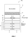
- FIG. 2 shows another embodiment magnetic tunnel junction 10a.
- the magnetic tunnel junction 10a comprises a first electrode 12 comprising recording material, and a tunnel insulator 16; analogous to the first electrode and tunnel insulator discussed above with reference to FIG. 1 .
- the stack 22 of FIG. 2 is shown to comprise alternating first and second layers 30 and 32; with the first layers comprising, consisting essentially of, or consisting of Co, and the second layers comprising, consisting essentially of, or consisting of Pt, Pd and/or Ni.
- the iridium-containing region 18 is over the stack 22, and the polarizer region 20 is over the region 18.
- the polarizer region 20 comprises a cobalt-containing material 36 directly against the iridium-containing region 18.
- the cobalt-containing material 36 may comprise, consist essentially of, or consist of cobalt.
- An advantage of utilizing cobalt-containing material 36 can be that the cobalt-containing material has good adhesion to the iridium-containing material of region 18. In this contact, the "adhesion" may be magnetic adhesion, meaning that there is enhanced coupling strength through the iridium.
- a buffer region 38 is over material 36, and the cobalt-and-iron-containing region 24 is over the buffer region.
- the buffer region 38 may comprise substantially amorphous buffer material; and may, for example, comprise, consist essentially of, or consist of one or more of tantalum, ruthenium, tungsten, molybdenum, etc.
- the buffer region may have a thickness of, for example, from about 1 ⁇ to about 5 ⁇ .
- the buffer region may be utilized as a bridge between a first crystalline lattice beneath the buffer region and a second crystalline lattice above the buffer region.
- the cobalt-containing adhesion material 36 may have the fcc 111 lattice of the underlying iridium-containing region, and the cobalt-and-iron-containing region 24 may have a bcc 001 lattice.
- the buffer region may be omitted, and a bcc lattice may be formed directly against an fcc lattice.
- the thickness of the buffer layer may be tuned for magnetoresistance.
- the composition of the buffer layer may be tuned to inhibit crystallization of cobalt-and-iron-containing region 24 until after deposition of tunnel insulator 16 (e.g., the buffer layer may comprise one or more of Ta, Mo, etc.).
- the polarizer region 20 may have a total thickness of from about 4 ⁇ to about 25 ⁇ ; the iridium-containing region 18 may have a total thickness of from about 2 ⁇ to about 20 ⁇ ; and the stack 22 may have a total thickness of from about 20 ⁇ to about 200 ⁇ .
- the stack 22 may have high perpendicular magnetic anisotropy.
- the iridium-containing region 18 may also have high perpendicular magnetic anisotropy, and further may be a barrier to diffusion of materials from stack 22 into polarizer region 20 and vice versa.
- the magnetic tunnel junctions discussed above may be utilized in memory products or specific memory technologies (e.g., MRAM. STT-MRAM, etc.), or in other technologies (e.g., logic, sensors, oscillators, etc.).
- the magnetic tunnel junctions may be incorporated into electronic systems.
- Such electronic systems may be used in, for example, memory modules, device drivers, power modules, communication modems, processor modules, and application-specific modules, and may include multilayer, multichip modules.
- the electronic systems may be any of a broad range of systems, such as, for example, cameras, wireless devices, displays, chip sets, set top boxes, games, lighting, vehicles, clocks, televisions, cell phones, personal computers, automobiles, industrial control systems, aircraft, etc.
- Some embodiments include a magnetic tunnel junction comprising magnetic reference material having an iridium-containing region between a multi-layer stack and a polarizer region.
- Some embodiments include a magnetic tunnel junction having a conductive first magnetic electrode which contains magnetic recording material, a conductive second magnetic electrode spaced from the first electrode and which contains magnetic reference material, and a non-magnetic insulator material between the first and second electrodes.
- the magnetic reference material of the second electrode includes an iridium-containing material over a stack comprising Co and one or more of platinum, palladium and nickel.
- the magnetic reference material includes a cobalt-and-iron-containing material over the iridium-containing material and directly against the non-magnetic insulator material.
- the iridium-containing material and the stack have a first crystalline lattice
- the non-magnetic insulator material and the cobalt-and-iron-containing material have a second crystalline lattice which is different from the first crystalline lattice.
- a buffer region is between the iridium-containing material and the cobalt-and-iron-containing material.
- Some embodiments include a magnetic tunnel junction having a conductive first magnetic electrode which contains magnetic recording material, a conductive second magnetic electrode spaced from the first electrode and which contains magnetic reference material, and a non-magnetic insulator material between the first and second electrodes.
- the magnetic reference material of the second electrode includes a stack of alternating first and second layers. The first layers comprise cobalt and the second layers comprise one or more of Pt, Pd and Ni.
- the magnetic reference material of the second electrode comprises an iridium-containing region over the stack.
- the magnetic reference material of the second electrode comprises a polarized region between the iridium-containing region and the non-magnetic insulator material.
- the polarized region includes a material comprising cobalt and iron.
Landscapes
- Engineering & Computer Science (AREA)
- Computer Hardware Design (AREA)
- Manufacturing & Machinery (AREA)
- Hall/Mr Elements (AREA)
- Mram Or Spin Memory Techniques (AREA)
- Thin Magnetic Films (AREA)
Claims (8)
- Magnetischer Tunnelübergang (10), Folgendes beinhaltet:eine erste leitfähige magnetische Elektrode (12), welche magnetisches Aufzeichnungsmaterial beinhaltet;eine zweite leitfähige magnetische Elektrode (14), welche von der ersten Elektrode (12) beabstandet ist und magnetisches Referenzmaterial beinhaltet;nichtmagnetisches Isolatormateriali (16) zwischen der ersten und der zweiten Elektrode;wobei das magnetische Referenzmaterial der zweiten Elektrode (14) einen iridiumhaltigen Bereich (18) über einem Stapel (22) beinhaltet, welcher Co und eines oder mehrere von Platin, Palladium und Nickel beinhaltet, wobei der iridiumhaltige Bereich (18) aus Iridium besteht;wobei das Referenzmaterial der zweiten Elektrode (14) ein Haftmaterial (36) beinhaltet, bestehend aus Kobalt, über und direkt an dem iridiumhaltigen Bereich (18), ein kobalt- und eisenhaltiges Material (24) direkt an dem nichtmagnetischen Isolatormaterial (16) und einen Pufferbereich (38) zwischen dem Haftlaterial (36) und dem kobalt- und eisenhaltigen Material (24); undwobei der iridiumhaltige Bereich (18) und der Stapel (22) ein erstes Kristallgitter aufweisen, und das nichtmagnetische Isolatormateriali (16) und das kobalt- und eisenhaltige Material (24) ein zweites Kristallgitter aufweisen, welches sich von dem ersten Kristallgitter unterscheidet.
- Magnetischer Tunnelübergang (10) nach Anspruch 1, bei welchem der iridiumhaltige Bereich (18) eine Dicke in einem Bereich von 2x 10⁻¹⁰ m bis 20x 10-10 m aufweist.
- Magnetischer Tunnelübergang (10) nach Anspruch 1, bei welchem das erste Kristallgitter kubisch-flächenzentriert (fcc) 111 ist; wobei das zweite Kristallgitter kubischraumzentriert (bcc) 001 ist.
- Magnetischer Tunnelübergang (10) nach Anspruch 1, bei welchem der Pufferbereich (38) aus einem oder mehreren von Tantal, Ruthenium, Wolfram und Molybdän besteht.
- Magnetischer Tunnelübergang (10) nach Anspruch 1, bei welchem der Pufferbereich (38) aus Tantal besteht.
- Magnetischer Tunnelübergang (10) nach Anspruch 1, bei welchem das kobalt- und eisenhaltige Material (24) zudem eines oder mehrere von B, Ta, W, Re und Mo beinhaltet.
- Magnetischer Tunnelübergang (10) nach Anspruch 1, bei welchem das kobalthaltige Haftmaterial (36) das erste Kristallgitter aufweist.
- Magnetischer Tunnelübergang (10) nach Anspruch 1, bei welchem der Pufferbereich (38) eine Dicke in einem Bereich von 1x 10⁻¹⁰ m bis 5x 10⁻¹⁰ m aufweist.
Applications Claiming Priority (2)
| Application Number | Priority Date | Filing Date | Title |
|---|---|---|---|
| US14/797,622 US9537088B1 (en) | 2015-07-13 | 2015-07-13 | Magnetic tunnel junctions |
| PCT/US2016/041449 WO2017011289A1 (en) | 2015-07-13 | 2016-07-08 | Magnetic tunnel junctions |
Publications (3)
| Publication Number | Publication Date |
|---|---|
| EP3323158A1 EP3323158A1 (de) | 2018-05-23 |
| EP3323158A4 EP3323158A4 (de) | 2019-03-27 |
| EP3323158B1 true EP3323158B1 (de) | 2020-03-18 |
Family
ID=57682438
Family Applications (1)
| Application Number | Title | Priority Date | Filing Date |
|---|---|---|---|
| EP16824930.8A Active EP3323158B1 (de) | 2015-07-13 | 2016-07-08 | Magnetische tunnelübergänge |
Country Status (7)
| Country | Link |
|---|---|
| US (1) | US9537088B1 (de) |
| EP (1) | EP3323158B1 (de) |
| JP (1) | JP6590351B2 (de) |
| KR (1) | KR102051728B1 (de) |
| CN (1) | CN107683507B (de) |
| TW (1) | TWI605451B (de) |
| WO (1) | WO2017011289A1 (de) |
Families Citing this family (12)
| Publication number | Priority date | Publication date | Assignee | Title |
|---|---|---|---|---|
| SG11201700861XA (en) * | 2014-09-25 | 2017-03-30 | Agency Science Tech & Res | Magnetic element and method of fabrication thereof |
| US10468590B2 (en) | 2015-04-21 | 2019-11-05 | Spin Memory, Inc. | High annealing temperature perpendicular magnetic anisotropy structure for magnetic random access memory |
| US9728712B2 (en) | 2015-04-21 | 2017-08-08 | Spin Transfer Technologies, Inc. | Spin transfer torque structure for MRAM devices having a spin current injection capping layer |
| US9853206B2 (en) | 2015-06-16 | 2017-12-26 | Spin Transfer Technologies, Inc. | Precessional spin current structure for MRAM |
| US9773974B2 (en) | 2015-07-30 | 2017-09-26 | Spin Transfer Technologies, Inc. | Polishing stop layer(s) for processing arrays of semiconductor elements |
| US10547067B2 (en) * | 2015-09-19 | 2020-01-28 | Daimler Ag | Shutdown and storage method for fuel cell system at below freezing temperatures |
| US9741926B1 (en) | 2016-01-28 | 2017-08-22 | Spin Transfer Technologies, Inc. | Memory cell having magnetic tunnel junction and thermal stability enhancement layer |
| US10361361B2 (en) * | 2016-04-08 | 2019-07-23 | International Business Machines Corporation | Thin reference layer for STT MRAM |
| US10665777B2 (en) | 2017-02-28 | 2020-05-26 | Spin Memory, Inc. | Precessional spin current structure with non-magnetic insertion layer for MRAM |
| US10672976B2 (en) | 2017-02-28 | 2020-06-02 | Spin Memory, Inc. | Precessional spin current structure with high in-plane magnetization for MRAM |
| US10784439B2 (en) * | 2017-12-29 | 2020-09-22 | Spin Memory, Inc. | Precessional spin current magnetic tunnel junction devices and methods of manufacture |
| US10580827B1 (en) | 2018-11-16 | 2020-03-03 | Spin Memory, Inc. | Adjustable stabilizer/polarizer method for MRAM with enhanced stability and efficient switching |
Family Cites Families (26)
| Publication number | Priority date | Publication date | Assignee | Title |
|---|---|---|---|---|
| US6960480B1 (en) * | 2004-05-19 | 2005-11-01 | Headway Technologies, Inc. | Method of forming a magnetic tunneling junction (MTJ) MRAM device and a tunneling magnetoresistive (TMR) read head |
| JP5077802B2 (ja) * | 2005-02-16 | 2012-11-21 | 日本電気株式会社 | 積層強磁性構造体、及び、mtj素子 |
| US7532442B2 (en) * | 2005-09-19 | 2009-05-12 | Hitachi Global Storage Technologies Netherlands B.V. | Magnetoresistive (MR) elements having pinning layers formed from permanent magnetic material |
| US7528457B2 (en) * | 2006-04-14 | 2009-05-05 | Magic Technologies, Inc. | Method to form a nonmagnetic cap for the NiFe(free) MTJ stack to enhance dR/R |
| US7595520B2 (en) * | 2006-07-31 | 2009-09-29 | Magic Technologies, Inc. | Capping layer for a magnetic tunnel junction device to enhance dR/R and a method of making the same |
| US8623452B2 (en) * | 2010-12-10 | 2014-01-07 | Avalanche Technology, Inc. | Magnetic random access memory (MRAM) with enhanced magnetic stiffness and method of making same |
| US8139325B2 (en) * | 2007-06-19 | 2012-03-20 | Canon Anelva Corporation | Tunnel magnetoresistive thin film |
| JP4649457B2 (ja) * | 2007-09-26 | 2011-03-09 | 株式会社東芝 | 磁気抵抗素子及び磁気メモリ |
| US7948044B2 (en) * | 2008-04-09 | 2011-05-24 | Magic Technologies, Inc. | Low switching current MTJ element for ultra-high STT-RAM and a method for making the same |
| WO2010080542A1 (en) | 2008-12-17 | 2010-07-15 | Yadav Technology, Inc. | Spin-transfer torque magnetic random access memory having magnetic tunnel junction with perpendicular magnetic anisotropy |
| US8445979B2 (en) * | 2009-09-11 | 2013-05-21 | Samsung Electronics Co., Ltd. | Magnetic memory devices including magnetic layers separated by tunnel barriers |
| US9082951B2 (en) | 2011-02-16 | 2015-07-14 | Avalanche Technology, Inc. | Magnetic random access memory with perpendicular enhancement layer |
| JP5177585B2 (ja) * | 2010-09-17 | 2013-04-03 | 株式会社東芝 | 磁気抵抗効果素子及び磁気メモリ |
| JP5148673B2 (ja) | 2010-09-17 | 2013-02-20 | 株式会社東芝 | 磁気抵抗効果素子及び磁気メモリ |
| JP2012160681A (ja) * | 2011-02-03 | 2012-08-23 | Sony Corp | 記憶素子、メモリ装置 |
| CN102298962A (zh) * | 2011-03-29 | 2011-12-28 | 清华大学 | 一种复合自由层stt-ram存储单元 |
| US8570691B2 (en) * | 2011-04-07 | 2013-10-29 | HGST Netherlands B.V. | TMR sensor film using a tantalum insertion layer and systems thereof |
| WO2013027406A1 (ja) * | 2011-08-25 | 2013-02-28 | キヤノンアネルバ株式会社 | 磁気抵抗効果素子の製造方法及び磁気抵抗効果膜の加工方法 |
| US9058885B2 (en) | 2011-12-07 | 2015-06-16 | Agency For Science, Technology And Research | Magnetoresistive device and a writing method for a magnetoresistive device |
| JP5836163B2 (ja) * | 2012-03-08 | 2015-12-24 | ルネサスエレクトロニクス株式会社 | 磁気メモリセル、磁気メモリセルの製造方法 |
| US8617644B2 (en) * | 2012-03-08 | 2013-12-31 | HGST Netherlands B.V. | Method for making a current-perpendicular-to-the-plane (CPP) magnetoresistive sensor containing a ferromagnetic alloy requiring post-deposition annealing |
| US8811072B2 (en) * | 2012-03-13 | 2014-08-19 | Honeywell International Inc. | Magnetoresistive random access memory (MRAM) package including a multilayer magnetic security structure |
| US8687415B2 (en) * | 2012-07-06 | 2014-04-01 | International Business Machines Corporation | Domain wall motion in perpendicularly magnetized wires having artificial antiferromagnetically coupled multilayers with engineered interfaces |
| US9214624B2 (en) * | 2012-07-27 | 2015-12-15 | Qualcomm Incorporated | Amorphous spacerlattice spacer for perpendicular MTJs |
| KR102114285B1 (ko) | 2013-04-09 | 2020-05-22 | 에스케이하이닉스 주식회사 | 반도체 장치 및 이 반도체 장치를 포함하는 마이크로프로세서, 프로세서, 시스템, 데이터 저장 시스템 및 메모리 시스템 |
| KR102126975B1 (ko) * | 2013-12-09 | 2020-06-25 | 삼성전자주식회사 | 자기 기억 소자 및 그 제조 방법 |
-
2015
- 2015-07-13 US US14/797,622 patent/US9537088B1/en active Active
-
2016
- 2016-07-08 WO PCT/US2016/041449 patent/WO2017011289A1/en not_active Ceased
- 2016-07-08 EP EP16824930.8A patent/EP3323158B1/de active Active
- 2016-07-08 JP JP2018500787A patent/JP6590351B2/ja active Active
- 2016-07-08 CN CN201680029604.6A patent/CN107683507B/zh active Active
- 2016-07-08 KR KR1020177037411A patent/KR102051728B1/ko active Active
- 2016-07-12 TW TW105121920A patent/TWI605451B/zh active
Non-Patent Citations (1)
| Title |
|---|
| None * |
Also Published As
| Publication number | Publication date |
|---|---|
| JP2018521511A (ja) | 2018-08-02 |
| JP6590351B2 (ja) | 2019-10-16 |
| US20170018705A1 (en) | 2017-01-19 |
| TWI605451B (zh) | 2017-11-11 |
| WO2017011289A1 (en) | 2017-01-19 |
| EP3323158A4 (de) | 2019-03-27 |
| TW201717199A (zh) | 2017-05-16 |
| US9537088B1 (en) | 2017-01-03 |
| EP3323158A1 (de) | 2018-05-23 |
| KR102051728B1 (ko) | 2019-12-03 |
| CN107683507A (zh) | 2018-02-09 |
| KR20180004834A (ko) | 2018-01-12 |
| CN107683507B (zh) | 2021-01-26 |
Similar Documents
| Publication | Publication Date | Title |
|---|---|---|
| US9537088B1 (en) | Magnetic tunnel junctions | |
| US10720569B2 (en) | Magnetic tunnel junctions | |
| US9059389B2 (en) | Free layers with iron interfacial layer and oxide cap for high perpendicular anisotropy energy density | |
| TWI602329B (zh) | 磁穿隧接面 | |
| EP3284117B1 (de) | Verfahren zur bildung einer magnetischen elektrode eines magnettunnelübergangs | |
| EP3231019B1 (de) | Magnetische tunnelübergänge | |
| EP3292571B1 (de) | Magnetische tunnelübergänge | |
| EP3284116B1 (de) | Magnetische tunnelübergänge | |
| US9478735B1 (en) | Magnetic tunnel junctions | |
| US12108686B2 (en) | Paramagnetic hexagonal metal phase coupling spacer |
Legal Events
| Date | Code | Title | Description |
|---|---|---|---|
| STAA | Information on the status of an ep patent application or granted ep patent |
Free format text: STATUS: THE INTERNATIONAL PUBLICATION HAS BEEN MADE |
|
| PUAI | Public reference made under article 153(3) epc to a published international application that has entered the european phase |
Free format text: ORIGINAL CODE: 0009012 |
|
| STAA | Information on the status of an ep patent application or granted ep patent |
Free format text: STATUS: REQUEST FOR EXAMINATION WAS MADE |
|
| 17P | Request for examination filed |
Effective date: 20180209 |
|
| AK | Designated contracting states |
Kind code of ref document: A1 Designated state(s): AL AT BE BG CH CY CZ DE DK EE ES FI FR GB GR HR HU IE IS IT LI LT LU LV MC MK MT NL NO PL PT RO RS SE SI SK SM TR |
|
| AX | Request for extension of the european patent |
Extension state: BA ME |
|
| RIN1 | Information on inventor provided before grant (corrected) |
Inventor name: MURTHY, SUNIL, S. Inventor name: CHEN, WEI Inventor name: HARMS, JONATHAN, D. |
|
| DAV | Request for validation of the european patent (deleted) | ||
| DAX | Request for extension of the european patent (deleted) | ||
| REG | Reference to a national code |
Ref country code: DE Ref legal event code: R079 Ref document number: 602016032228 Country of ref document: DE Free format text: PREVIOUS MAIN CLASS: H01L0043020000 Ipc: G11C0011160000 |
|
| A4 | Supplementary search report drawn up and despatched |
Effective date: 20190227 |
|
| RIC1 | Information provided on ipc code assigned before grant |
Ipc: H01L 43/08 20060101ALI20190221BHEP Ipc: H01L 43/10 20060101ALI20190221BHEP Ipc: H01L 43/02 20060101ALI20190221BHEP Ipc: G11C 11/16 20060101AFI20190221BHEP |
|
| GRAP | Despatch of communication of intention to grant a patent |
Free format text: ORIGINAL CODE: EPIDOSNIGR1 |
|
| STAA | Information on the status of an ep patent application or granted ep patent |
Free format text: STATUS: GRANT OF PATENT IS INTENDED |
|
| INTG | Intention to grant announced |
Effective date: 20191105 |
|
| GRAS | Grant fee paid |
Free format text: ORIGINAL CODE: EPIDOSNIGR3 |
|
| GRAA | (expected) grant |
Free format text: ORIGINAL CODE: 0009210 |
|
| STAA | Information on the status of an ep patent application or granted ep patent |
Free format text: STATUS: THE PATENT HAS BEEN GRANTED |
|
| AK | Designated contracting states |
Kind code of ref document: B1 Designated state(s): AL AT BE BG CH CY CZ DE DK EE ES FI FR GB GR HR HU IE IS IT LI LT LU LV MC MK MT NL NO PL PT RO RS SE SI SK SM TR |
|
| REG | Reference to a national code |
Ref country code: GB Ref legal event code: FG4D |
|
| REG | Reference to a national code |
Ref country code: DE Ref legal event code: R096 Ref document number: 602016032228 Country of ref document: DE |
|
| REG | Reference to a national code |
Ref country code: AT Ref legal event code: REF Ref document number: 1246845 Country of ref document: AT Kind code of ref document: T Effective date: 20200415 Ref country code: IE Ref legal event code: FG4D |
|
| PG25 | Lapsed in a contracting state [announced via postgrant information from national office to epo] |
Ref country code: RS Free format text: LAPSE BECAUSE OF FAILURE TO SUBMIT A TRANSLATION OF THE DESCRIPTION OR TO PAY THE FEE WITHIN THE PRESCRIBED TIME-LIMIT Effective date: 20200318 Ref country code: FI Free format text: LAPSE BECAUSE OF FAILURE TO SUBMIT A TRANSLATION OF THE DESCRIPTION OR TO PAY THE FEE WITHIN THE PRESCRIBED TIME-LIMIT Effective date: 20200318 Ref country code: NO Free format text: LAPSE BECAUSE OF FAILURE TO SUBMIT A TRANSLATION OF THE DESCRIPTION OR TO PAY THE FEE WITHIN THE PRESCRIBED TIME-LIMIT Effective date: 20200618 |
|
| REG | Reference to a national code |
Ref country code: NL Ref legal event code: MP Effective date: 20200318 |
|
| PG25 | Lapsed in a contracting state [announced via postgrant information from national office to epo] |
Ref country code: GR Free format text: LAPSE BECAUSE OF FAILURE TO SUBMIT A TRANSLATION OF THE DESCRIPTION OR TO PAY THE FEE WITHIN THE PRESCRIBED TIME-LIMIT Effective date: 20200619 Ref country code: BG Free format text: LAPSE BECAUSE OF FAILURE TO SUBMIT A TRANSLATION OF THE DESCRIPTION OR TO PAY THE FEE WITHIN THE PRESCRIBED TIME-LIMIT Effective date: 20200618 Ref country code: HR Free format text: LAPSE BECAUSE OF FAILURE TO SUBMIT A TRANSLATION OF THE DESCRIPTION OR TO PAY THE FEE WITHIN THE PRESCRIBED TIME-LIMIT Effective date: 20200318 Ref country code: LV Free format text: LAPSE BECAUSE OF FAILURE TO SUBMIT A TRANSLATION OF THE DESCRIPTION OR TO PAY THE FEE WITHIN THE PRESCRIBED TIME-LIMIT Effective date: 20200318 Ref country code: SE Free format text: LAPSE BECAUSE OF FAILURE TO SUBMIT A TRANSLATION OF THE DESCRIPTION OR TO PAY THE FEE WITHIN THE PRESCRIBED TIME-LIMIT Effective date: 20200318 |
|
| REG | Reference to a national code |
Ref country code: LT Ref legal event code: MG4D |
|
| PG25 | Lapsed in a contracting state [announced via postgrant information from national office to epo] |
Ref country code: NL Free format text: LAPSE BECAUSE OF FAILURE TO SUBMIT A TRANSLATION OF THE DESCRIPTION OR TO PAY THE FEE WITHIN THE PRESCRIBED TIME-LIMIT Effective date: 20200318 |
|
| PG25 | Lapsed in a contracting state [announced via postgrant information from national office to epo] |
Ref country code: LT Free format text: LAPSE BECAUSE OF FAILURE TO SUBMIT A TRANSLATION OF THE DESCRIPTION OR TO PAY THE FEE WITHIN THE PRESCRIBED TIME-LIMIT Effective date: 20200318 Ref country code: SK Free format text: LAPSE BECAUSE OF FAILURE TO SUBMIT A TRANSLATION OF THE DESCRIPTION OR TO PAY THE FEE WITHIN THE PRESCRIBED TIME-LIMIT Effective date: 20200318 Ref country code: RO Free format text: LAPSE BECAUSE OF FAILURE TO SUBMIT A TRANSLATION OF THE DESCRIPTION OR TO PAY THE FEE WITHIN THE PRESCRIBED TIME-LIMIT Effective date: 20200318 Ref country code: PT Free format text: LAPSE BECAUSE OF FAILURE TO SUBMIT A TRANSLATION OF THE DESCRIPTION OR TO PAY THE FEE WITHIN THE PRESCRIBED TIME-LIMIT Effective date: 20200812 Ref country code: EE Free format text: LAPSE BECAUSE OF FAILURE TO SUBMIT A TRANSLATION OF THE DESCRIPTION OR TO PAY THE FEE WITHIN THE PRESCRIBED TIME-LIMIT Effective date: 20200318 Ref country code: SM Free format text: LAPSE BECAUSE OF FAILURE TO SUBMIT A TRANSLATION OF THE DESCRIPTION OR TO PAY THE FEE WITHIN THE PRESCRIBED TIME-LIMIT Effective date: 20200318 Ref country code: IS Free format text: LAPSE BECAUSE OF FAILURE TO SUBMIT A TRANSLATION OF THE DESCRIPTION OR TO PAY THE FEE WITHIN THE PRESCRIBED TIME-LIMIT Effective date: 20200718 Ref country code: CZ Free format text: LAPSE BECAUSE OF FAILURE TO SUBMIT A TRANSLATION OF THE DESCRIPTION OR TO PAY THE FEE WITHIN THE PRESCRIBED TIME-LIMIT Effective date: 20200318 |
|
| REG | Reference to a national code |
Ref country code: AT Ref legal event code: MK05 Ref document number: 1246845 Country of ref document: AT Kind code of ref document: T Effective date: 20200318 |
|
| REG | Reference to a national code |
Ref country code: DE Ref legal event code: R097 Ref document number: 602016032228 Country of ref document: DE |
|
| PLBE | No opposition filed within time limit |
Free format text: ORIGINAL CODE: 0009261 |
|
| STAA | Information on the status of an ep patent application or granted ep patent |
Free format text: STATUS: NO OPPOSITION FILED WITHIN TIME LIMIT |
|
| PG25 | Lapsed in a contracting state [announced via postgrant information from national office to epo] |
Ref country code: ES Free format text: LAPSE BECAUSE OF FAILURE TO SUBMIT A TRANSLATION OF THE DESCRIPTION OR TO PAY THE FEE WITHIN THE PRESCRIBED TIME-LIMIT Effective date: 20200318 Ref country code: DK Free format text: LAPSE BECAUSE OF FAILURE TO SUBMIT A TRANSLATION OF THE DESCRIPTION OR TO PAY THE FEE WITHIN THE PRESCRIBED TIME-LIMIT Effective date: 20200318 Ref country code: IT Free format text: LAPSE BECAUSE OF FAILURE TO SUBMIT A TRANSLATION OF THE DESCRIPTION OR TO PAY THE FEE WITHIN THE PRESCRIBED TIME-LIMIT Effective date: 20200318 Ref country code: AT Free format text: LAPSE BECAUSE OF FAILURE TO SUBMIT A TRANSLATION OF THE DESCRIPTION OR TO PAY THE FEE WITHIN THE PRESCRIBED TIME-LIMIT Effective date: 20200318 |
|
| 26N | No opposition filed |
Effective date: 20201221 |
|
| PG25 | Lapsed in a contracting state [announced via postgrant information from national office to epo] |
Ref country code: MC Free format text: LAPSE BECAUSE OF FAILURE TO SUBMIT A TRANSLATION OF THE DESCRIPTION OR TO PAY THE FEE WITHIN THE PRESCRIBED TIME-LIMIT Effective date: 20200318 Ref country code: PL Free format text: LAPSE BECAUSE OF FAILURE TO SUBMIT A TRANSLATION OF THE DESCRIPTION OR TO PAY THE FEE WITHIN THE PRESCRIBED TIME-LIMIT Effective date: 20200318 |
|
| REG | Reference to a national code |
Ref country code: CH Ref legal event code: PL |
|
| REG | Reference to a national code |
Ref country code: BE Ref legal event code: MM Effective date: 20200731 |
|
| PG25 | Lapsed in a contracting state [announced via postgrant information from national office to epo] |
Ref country code: LU Free format text: LAPSE BECAUSE OF NON-PAYMENT OF DUE FEES Effective date: 20200708 Ref country code: LI Free format text: LAPSE BECAUSE OF NON-PAYMENT OF DUE FEES Effective date: 20200731 Ref country code: CH Free format text: LAPSE BECAUSE OF NON-PAYMENT OF DUE FEES Effective date: 20200731 |
|
| PG25 | Lapsed in a contracting state [announced via postgrant information from national office to epo] |
Ref country code: BE Free format text: LAPSE BECAUSE OF NON-PAYMENT OF DUE FEES Effective date: 20200731 Ref country code: SI Free format text: LAPSE BECAUSE OF FAILURE TO SUBMIT A TRANSLATION OF THE DESCRIPTION OR TO PAY THE FEE WITHIN THE PRESCRIBED TIME-LIMIT Effective date: 20200318 |
|
| PG25 | Lapsed in a contracting state [announced via postgrant information from national office to epo] |
Ref country code: IE Free format text: LAPSE BECAUSE OF NON-PAYMENT OF DUE FEES Effective date: 20200708 |
|
| PG25 | Lapsed in a contracting state [announced via postgrant information from national office to epo] |
Ref country code: TR Free format text: LAPSE BECAUSE OF FAILURE TO SUBMIT A TRANSLATION OF THE DESCRIPTION OR TO PAY THE FEE WITHIN THE PRESCRIBED TIME-LIMIT Effective date: 20200318 Ref country code: MT Free format text: LAPSE BECAUSE OF FAILURE TO SUBMIT A TRANSLATION OF THE DESCRIPTION OR TO PAY THE FEE WITHIN THE PRESCRIBED TIME-LIMIT Effective date: 20200318 Ref country code: CY Free format text: LAPSE BECAUSE OF FAILURE TO SUBMIT A TRANSLATION OF THE DESCRIPTION OR TO PAY THE FEE WITHIN THE PRESCRIBED TIME-LIMIT Effective date: 20200318 |
|
| PG25 | Lapsed in a contracting state [announced via postgrant information from national office to epo] |
Ref country code: MK Free format text: LAPSE BECAUSE OF FAILURE TO SUBMIT A TRANSLATION OF THE DESCRIPTION OR TO PAY THE FEE WITHIN THE PRESCRIBED TIME-LIMIT Effective date: 20200318 Ref country code: AL Free format text: LAPSE BECAUSE OF FAILURE TO SUBMIT A TRANSLATION OF THE DESCRIPTION OR TO PAY THE FEE WITHIN THE PRESCRIBED TIME-LIMIT Effective date: 20200318 |
|
| PGFP | Annual fee paid to national office [announced via postgrant information from national office to epo] |
Ref country code: DE Payment date: 20250728 Year of fee payment: 10 |
|
| PGFP | Annual fee paid to national office [announced via postgrant information from national office to epo] |
Ref country code: GB Payment date: 20250722 Year of fee payment: 10 |
|
| PGFP | Annual fee paid to national office [announced via postgrant information from national office to epo] |
Ref country code: FR Payment date: 20250725 Year of fee payment: 10 |