EP3321981B1 - Stromquellenvorrichtung und lichtstrahlungssystem damit - Google Patents
Stromquellenvorrichtung und lichtstrahlungssystem damit Download PDFInfo
- Publication number
- EP3321981B1 EP3321981B1 EP16821179.5A EP16821179A EP3321981B1 EP 3321981 B1 EP3321981 B1 EP 3321981B1 EP 16821179 A EP16821179 A EP 16821179A EP 3321981 B1 EP3321981 B1 EP 3321981B1
- Authority
- EP
- European Patent Office
- Prior art keywords
- resistance
- voltage dividing
- light source
- power source
- identification
- Prior art date
- Legal status (The legal status is an assumption and is not a legal conclusion. Google has not performed a legal analysis and makes no representation as to the accuracy of the status listed.)
- Active
Links
- 230000005855 radiation Effects 0.000 title claims description 44
- 238000005259 measurement Methods 0.000 description 14
- 238000004519 manufacturing process Methods 0.000 description 4
- 238000010586 diagram Methods 0.000 description 3
- 230000007547 defect Effects 0.000 description 2
- 230000006866 deterioration Effects 0.000 description 2
- 230000000694 effects Effects 0.000 description 2
- 230000006870 function Effects 0.000 description 2
- 238000003848 UV Light-Curing Methods 0.000 description 1
- 239000004065 semiconductor Substances 0.000 description 1
Images


Classifications
-
- H—ELECTRICITY
- H05—ELECTRIC TECHNIQUES NOT OTHERWISE PROVIDED FOR
- H05B—ELECTRIC HEATING; ELECTRIC LIGHT SOURCES NOT OTHERWISE PROVIDED FOR; CIRCUIT ARRANGEMENTS FOR ELECTRIC LIGHT SOURCES, IN GENERAL
- H05B45/00—Circuit arrangements for operating light-emitting diodes [LED]
- H05B45/40—Details of LED load circuits
-
- H—ELECTRICITY
- H01—ELECTRIC ELEMENTS
- H01L—SEMICONDUCTOR DEVICES NOT COVERED BY CLASS H10
- H01L33/00—Semiconductor devices having potential barriers specially adapted for light emission; Processes or apparatus specially adapted for the manufacture or treatment thereof or of parts thereof; Details thereof
-
- H—ELECTRICITY
- H05—ELECTRIC TECHNIQUES NOT OTHERWISE PROVIDED FOR
- H05B—ELECTRIC HEATING; ELECTRIC LIGHT SOURCES NOT OTHERWISE PROVIDED FOR; CIRCUIT ARRANGEMENTS FOR ELECTRIC LIGHT SOURCES, IN GENERAL
- H05B45/00—Circuit arrangements for operating light-emitting diodes [LED]
- H05B45/30—Driver circuits
- H05B45/345—Current stabilisation; Maintaining constant current
Definitions
- This invention relates to a power source device to be connected to a light radiation device and a light radiation system using the power source device.
- this kind of the power source device is configured to be connected to the light radiation device comprising a light source and an identification resistance whose resistance value differs for each type of the light source, and the type of the light source is automatically determined and the light source can be controlled to change the brightness of the electric light in accordance with the determined type of the light source.
- the power source device has a voltage dividing resistance connected in series to the identification resistance, the divided voltage applied to the voltage dividing resistance is measured, and the type of the light source is determined based on the measured divided voltage value.
- the type of the light source is determined based on the divided voltage value, it is necessary to select the identification resistance among a limited range of the resistance value in order for the divided voltage value to fall within the measurement range.
- the resistance value of the identification resistance contains a manufacturing error, if the resistance value of the identification resistance of each light source is close to each other, it is not possible to distinguish whether the difference in the measured divided voltage value appears due to the type of the light source or due to the manufacturing error of the identification resistance.
- the type of the resistance value that can be used as the identification resistance is limited so that the present structure can determine only limited types of the light source, and the number of these types is not satisfactory at all.
- JP S58 106470 A discloses a high resistance measuring device.
- JP 2004 158840 A discloses a power supply system for LED lighting devices.
- the present claimed invention intends to solve all of the above-mentioned problems, and a main object of this invention is to increase a number of a type of a light source that can be determined by widening a range of a resistance value of a resistance that can be used as an identification resistance.
- the power source device in accordance with this present claimed invention is a power source device to be connected to a light radiation device, said light radiation device comprises a light source having one or a plurality of LEDs and an identification resistance whose resistance value is different for each type of the light source, and said power source device comprises a power source configured to apply a voltage to the light radiation device and an identification resistance determination circuit that has a voltage dividing resistance to be connected to the identification resistance in series, and a control unit that measures a divided voltage applied to the voltage dividing resistance, determines the type of the light source based on the divided voltage value, and controls a power to the light source according to the type thereof, and the identification resistance determination circuit comprises a plurality of voltage dividing resistances, each of which has a different resistance value, and is configured such that the voltage dividing resistance to be connected to the identification resistance can be switched.
- the power source device having this arrangement, since a plurality of the voltage dividing resistances whose resistance values differ from each other are switchably provided for the identification resistance determination circuit, the range of the resistance value of the identification resistance wherein the divided voltage value can fall within the measurement range is changed by switching the voltage dividing resistance. With this arrangement, it is possible to increase the number of the type of the light source that can be determined by widening the range of the resistance value of the identification resistance that can be used.
- the identification resistance determination circuit comprises a first voltage dividing resistance and a second voltage dividing resistance whose resistance value is different from that of the first voltage dividing resistance, and in a case that it is not possible to determine the type of the light source based on the divided voltage applied to the first voltage dividing resistance, the control unit is configured to switch the voltage dividing resistance to be connected to the identification resistance from the first voltage dividing resistance to the second voltage dividing resistance.
- control unit is configured to output a signal indicating that the determination is not possible.
- control unit has a determination data memory part that stores determination data wherein the divided voltage value of the voltage dividing resistance is associated with information relating to the type of the light source, and the determination data memory part stores a plurality of items of the determination data, each of which corresponds to each of the voltage dividing resistances respectively in a state of being combined with each of the voltage dividing resistances.
- a light radiation system in accordance with this invention comprises a light radiation device provided with a light source having one or a plurality of LEDs and an identification resistance whose resistance value is different for each type of the light source, and the power source device described in claim 1 is connected to the light radiation device. Also in accordance with this arrangement of the light radiation system, it is possible to obtain the same effect and operation as that of the above-mentioned power source device.
- the present claimed invention having the above-mentioned arrangement, since it is possible to widen a range of the resister value that can be utilized as the identification resistance, the number of the type of the light source that can be determined can be increased.
- the invention is defined by the subject-matter of claim 1.
- the light radiation system 100 in accordance with this embodiment comprises, as shown in Fig. 1 , an LED light radiation device 10 as a light radiation device, and a power source device 20 to which the LED light radiation device 10 is connected, and is of, for example, a constant current type.
- the LED light radiation device 10 is connected to the power source device 20; however, a light radiation device that is loaded with LEDs that irradiate ultraviolet rays and that is used for UV curing may be connected to the power source device 20.
- the LED light radiation device 10 is connected to the power source device 20 through a connector, not shown in the drawings, and comprises a light source 12 having one or a plurality of LEDs 11 and an identification resistance 13 whose resistance value is different for each type of the light source 12.
- the light source 12 (the LED light radiation device 10) with specifications such as a rated current or a rated voltage, or a number or a characteristic of the LEDs 11 is different
- a different resistance value is set for the identification resistance 13 according to the type of the light source 12 in order to identify the type of the light source 12 (the LED light radiation device 10)
- the light source 12 comprises a resistor arranged in parallel to the LEDs 11 in this embodiment.
- Eight types of the light sources 12 (the LED light radiation device 10) whose rated currents are different from each other are prepared in this embodiment (one of the light sources 12 is shown in Fig. 1 ), and 2.7 k ⁇ , 3.9 k ⁇ , 5.6 k ⁇ , 8.2 k ⁇ , 12 k ⁇ , 22 k ⁇ , 36 k ⁇ , and 60 k ⁇ are used for these identification resistances 13.
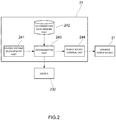
- the power source device 20 is to supply an electric power to the LED light radiation device 10 to which the power source device 20 is connected, and comprises, as shown in Fig. 1 , a variable power source 21 to be connected to the light source 12, a constant current control circuit 22 that controls the electric current supplied to the light source 12 so as to be constant, an identification resistance determination circuit 23 to determine a resistance value of the identification resistance 13, and a control unit 24 that is connected to the identification resistance determination circuit 23.
- the variable power source 21 is configured to apply a predetermined DC voltage to the light source 12, and the applied voltage is set so as to flow a rated current in the light source 12 based on a voltage command value from the control unit 24, to be described later.
- the constant current control circuit 22 performs analog control on the current flowing in the light source 12 by feedback control, and as shown concretely in Fig. 1 , is configured by making use of an operational amplifier 221 and an FET 222.
- the rated current of the light source 12 is input to the operational amplifier 221 as a target current by the control unit 24, to be described later.
- the identification resistance determination circuit 23 has a voltage dividing resistance 231 connected in series to the identification resistance 13, and is configured to divide the applied voltage of the variable power source 21 into the identification resistance 13 and the voltage dividing resistance 231.
- the identification resistance determination circuit 23 of this embodiment comprises, as shown in Fig. 1 , a plurality of voltage dividing resistances 231 whose resistance values differ from each other, and the voltage dividing resistance 231 to be connected to the identification resistance 13 can be switched to the other voltage dividing resistance 231. More concretely, the identification resistance determination circuit 23 is provided with a first voltage dividing resistance 231a and a second voltage dividing resistance 231b having a resistance larger than that of the first voltage dividing resistance 231a in parallel, and the first voltage dividing resistance 231a or the second voltage dividing resistance 231b can be alternatively connected to the identification resistance 13 by the use of a switch 232 such as, for example, a semiconductor switching element.
- the resistance value of the first voltage dividing resistance 231a is 3.3 k ⁇
- the resistance value of the second voltage dividing resistance 231b is 15 k ⁇ .
- control unit 24 comprises a CPU, a memory, and an input device or the like, and as shown in Fig. 2 , produces functions as a divided voltage measurement part 241, a determination data memory part 242, a determination part 243, and a power source control unit 244 by operating according to predetermined programs stored in the memory.
- the divided voltage measurement part 241 measures a divided voltage applied to the voltage dividing resistance 231 within a predetermined measurement range and outputs the divided voltage value to the determination part 243, and is configured by making use of an A/D board having, for example, a predetermined resolution.
- the determination data memory part 242 is formed in a predetermined area of the memory, and stores determination data wherein information relating to the type of the light source 12 is associated with the divided voltage value measured by the divided voltage measurement part 241.
- the divided voltage value corresponding to the type of each light source 12 is stored with a margin of error in consideration of the above-mentioned manufacturing error.
- the determination data memory part 242 of this embodiment stores the data as, for example, a lookup table by combining the resistance value of each identification resistance 13 with a predetermined range of the divided voltage value corresponding to each resistance value (hereinafter also referred to as a divided voltage value width).
- Adjacent divided voltage value widths are set not to overlap each other based on the divided voltage value (V) (a theoretical value) calculated by the above-mentioned expression (1).
- a plurality of voltage dividing resistances 231 are provided, and the determination data memory part 242 stores each of the determination data that is different for each of the voltage dividing resistances 231.
- the determination data memory part 242 stores the first determination data corresponding to the first voltage dividing resistance 231a and the second determination data corresponding to the second voltage dividing resistance 231b to be combined with each voltage dividing resistance 231.
- the determination part 243 obtains the divided voltage value from the divided voltage measurement part 241, refers to the determination data stored in the determination data memory part 242, and determines the type of the light source 12 that corresponds to the obtained divided voltage value.
- the determination part 243 detects which of the first voltage dividing resistance 231a and the second voltage dividing resistance 231b is connected to the identification resistance 13, refers to the determination data that corresponds to the connected voltage dividing resistance 231 and determines the divided voltage value width in which the divided voltage value is contained. Then the determination part 243 determines the type of the light source 12 based on the resistance value of the identification resistance 13 corresponding to the divided voltage value width and outputs an identification signal, according to the type of the light source 12, to the power source control unit 244.
- the power source control unit 244 obtains the identification signal from the above-mentioned determination part 243, and controls the variable power source 21 by outputting a control signal to the variable power source 21 in accordance with the type of the light source 12. More concretely, the power source control unit 244 controls an electric current or a voltage of the variable power source 21 appropriately for each type of the light source 12 based on the information contained in the identification signal such as, for example, a rated current, a rated voltage, an upper limit electric current and an upper limit voltage, or the information contained in the identification signal such as a number or a characteristic of the LED 11.
- the power source control unit 244 in this embodiment is configured to control an applied voltage of the variable power source 21 so as to flow the rated electric current in the light source 12, and to input the rated electric current to an operational amplifier 221 of the constant current control circuit 22 as a target electric current.
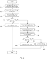
- the determination part 243 When the LED light radiation device 10 is connected to the power source 20, first the determination part 243 outputs a switch signal to the switch 232 and connects the first voltage dividing resistance 231a to the identification resistance 13 (S1).
- the power source control unit 244 outputs a control signal to the variable power source 21 and applies the predetermined voltage (for example, 5V) to the identification resistance 13, and the divided voltage measurement part 241 measures the divided voltage value of the first voltage dividing resistance 231a (S2).
- the predetermined voltage for example, 5V
- the determination part 243 obtains the divided voltage value of the first voltage dividing resistance 231a from the divided voltage measurement part 241, refers to the first determination data stored in the determination data memory part 242, detects the divided voltage value width in which the divided voltage value is contained, and determines the type of the light source 12 (S3).
- the determination part 243 outputs the identification signal according to the type of the determined light source 12 to the power source control unit 244, and the power source control unit 244 controls the variable power source 21 based on the identification signal (S5).
- the determination part 243 outputs the switch signal to the switch 232 and switches the voltage dividing resistance 231 to be connected to the identification resistance 13 from the first voltage dividing resistance 231a to the second voltage dividing resistance 231b (S6).
- the divided voltage measurement part 241 measures the divided voltage value of the second voltage dividing resistance 231b (S7), and the determination part 243 refers to the second determination data stored in the determination data memory part 242 and determines the type of the light source 12 (S8).
- the identification signal according to the type of the light source 12 is output to the power source control unit 244 and the power source control unit 244 controls the variable power source 21 based on the identification signal (S10).
- the determination part 243 In the case that the determination part 243 is unable to determine the type of the light source 12 based on the divided voltage value of the second voltage dividing resistance 231b (S9), the determination part 243 in this embodiment outputs a signal indicating that the determination is not possible and reports the user that the type of the light source 12 is unable to be determined (S11).
- the range of the resistance value of the identification resistance 13 wherein the divided voltage value can fall in the measurement range of the divided voltage measurement part 241 is changed by switching the voltage dividing resistance 231 by the determination part 243.
- the resistance value (r) of the voltage dividing resistance 231 increases by switching from the first voltage dividing resistance 231a to the second voltage dividing resistance 231b, even though the identification resistance 13 whose resistance value (R) is big is used, it is possible to increase the divided voltage value (V) to be measured.
- the resistance value (R) that can be used as the identification resistance 13 so that it is possible to increase the number of the types of the light source 12 that can be determined.
- the determination part 243 determines the type of the light source 12, and the voltage dividing resistance 231 to be connected to the identification resistance 13 is configured to be switchable to the other voltage dividing resistance 231, it is possible to automatically determine more numerous types of the light source 12, without reducing usability for the user.
- the determination part 243 outputs the signal indicting that the determination is not possible in the case that the type of the light source 12 is unable to be determined also by the divided voltage value (V) of the second voltage dividing resistance 231b, it is possible to notify the user that there is a defect in the LED light radiation device 10 or the power source device 20 due to deterioration of, for example, the identification resistance 13 or the voltage dividing resistance 231, or that an LED light radiation device 10 that does not correspond to the power source device 20 is connected.
- V divided voltage value
- the identification resistance 13 and the voltage dividing resistance 231 are the resistance; however, they may be a condenser or an inductance having predetermined impedance.
- a condenser having a different capacity for each type of the light source 12 is arranged instead of the identification resistance 13, and a condenser having a predetermined capacity is arranged instead of the voltage dividing resistance 231.
- the identification resistance determination circuit 23 of the above-mentioned embodiment has two voltage dividing resistances 231; however, it also may have an arrangement having three or more voltage dividing resistances 231 arranged in parallel.
- the light source 12 of the above-mentioned embodiment has a plurality of the LEDs 11 connected in series; however, it also may have a single LED 11, or may have a plurality of LEDs 11 connected in parallel.
- the determination part 243 outputs the switch signal to the switch 232 and switches the voltage dividing resistance 231; however, it may also be so arranged that an operator inputs the switch signal from the outside and switches the voltage dividing resistance 231.
- the power source control unit 244 of the above-mentioned embodiment is configured so that the variable power source 21 is controlled so as to flow the rated current in the light source 12; however, the variable power source 21 may also be controlled so as to apply the rated voltage to the light source 12.
- the light radiation system 100 of the above-mentioned embodiment is a constant current type; however, it also may be a constant voltage type.
- the range of the resistance value that can be utilized as the identification resistance can be widened, it is possible to increase the number of the type of the light source that can be determined.
Landscapes
- Engineering & Computer Science (AREA)
- Manufacturing & Machinery (AREA)
- Computer Hardware Design (AREA)
- Microelectronics & Electronic Packaging (AREA)
- Power Engineering (AREA)
- Led Devices (AREA)
- Circuit Arrangement For Electric Light Sources In General (AREA)
Claims (5)
- Stromquellenvorrichtung (20), die mit einer Lichtabstrahlungsvorrichtung (10) zu verbinden ist, wobei die Lichtabstrahlungsvorrichtung (10) eine Lichtquelle (12) mit einer oder mehreren LEDs (11) und einen Identifikationswiderstand (13) aufweist, dessen Widerstandswert für jeden Typ der Lichtquelle (12) unterschiedlich ist, wobei die Stromquellenvorrichtung (20) aufweist:eine Stromquelle (21), die dazu eingerichtet ist, dass sie eine Spannung (E) an die Lichtabstrahlungsvorrichtung (10) anlegt;eine Identifikationswiderstands-Bestimmungsschaltung (23), die einen Spannungsteilerwiderstand (231) aufweist, der mit dem Identifikationswiderstand (13) in Reihe zu schalten ist; undeine Steuereinheit (24), die eine an den Spannungsteilerwiderstand (231) angelegte geteilte Spannung misst, den Typ der Lichtquelle (12) auf der Grundlage des Wertes der geteilten Spannung bestimmt und eine Leistung für die Lichtquelle (12) entsprechend dem Typ derselben steuert,
dadurch gekennzeichnet, dassdie Identifikationswiderstands-Bestimmungsschaltung (23) eine Vielzahl von Spannungsteilerwiderständen (231a, 231b) aufweist, von denen jeder einen unterschiedlichen Widerstandswert aufweist, und so eingerichtet ist, dass der mit dem Identifikationswiderstand (13) zu verbindende Spannungsteilerwiderstand (231) geschaltet werden kann. - Stromquellenvorrichtung nach Anspruch 1, wobei
die Identifikationswiderstands-Bestimmungsschaltung (23) einen ersten Spannungsteilerwiderstand (231a) und einen zweiten Spannungsteilerwiderstand (231b) umfasst, dessen Widerstandswert sich von dem des ersten Spannungsteilerwiderstandes (231a) unterscheidet, und
in einem Fall, in dem es nicht möglich ist, den Typ der Lichtquelle (12) auf der Grundlage der an den ersten Spannungsteilerwiderstand (231a) angelegten geteilten Spannung zu bestimmen, ist die Steuereinheit (24) so eingerichtet, dass sie den an den Identifikationswiderstand (13) anzuschließenden Spannungsteilerwiderstand (231) von dem ersten Spannungsteilerwiderstand (231a) auf den zweiten Spannungsteilerwiderstand (231b) umschaltet. - Stromquellenvorrichtung nach Anspruch 2, wobei
in einem Fall, in dem es nicht möglich ist, den Typ der Lichtquelle (12) auf der Grundlage der an den zweiten Spannungsteilerwiderstand (231b) angelegten geteilten Spannung zu bestimmen, ist die Steuereinheit (24) so eingerichtet, dass sie ein Signal ausgibt, das anzeigt, dass die Bestimmung nicht möglich ist. - Stromquellenvorrichtung nach Anspruch 1, wobei
die Steuereinheit (24) einen Bestimmungsdaten-Speicherteil aufweist, der Bestimmungsdaten speichert, bei denen der geteilte Spannungswert des Spannungsteilerwiderstandes (231) mit Informationen verbunden ist, die sich auf den Typ der Lichtquelle (12) beziehen, und
der Bestimmungsdaten-Speicherteil eine Vielzahl von Elementen von Bestimmungsdaten speichert, von denen jedes jedem der Spannungsteilerwiderstände (231a, 231b) entspricht, die sich jeweils in einem Zustand befinden, in dem sie mit jedem der Spannungsteilerwiderstände (231a, 231b) kombiniert sind. - Ein Lichtabstrahlungssystem, aufweisend:eine Lichtabstrahlungsvorrichtung (10), die mit einer Lichtquelle (12) mit einer oder mehreren LEDs (11) und einem Identifikationswiderstand (13) versehen ist, dessen Widerstandswert für jeden Typ der Lichtquelle (12) unterschiedlich ist, unddie in Anspruch 1 beschriebene Stromquellenvorrichtung (20), die an die Lichtabstrahlungsvorrichtung (10) angeschlossen ist.
Applications Claiming Priority (2)
| Application Number | Priority Date | Filing Date | Title |
|---|---|---|---|
| JP2015136605A JP6654367B2 (ja) | 2015-07-08 | 2015-07-08 | 電源装置及びこれを備えた光照射システム |
| PCT/JP2016/067517 WO2017006709A1 (ja) | 2015-07-08 | 2016-06-13 | 電源装置及びこれを備えた光照射システム |
Publications (3)
| Publication Number | Publication Date |
|---|---|
| EP3321981A1 EP3321981A1 (de) | 2018-05-16 |
| EP3321981A4 EP3321981A4 (de) | 2019-01-16 |
| EP3321981B1 true EP3321981B1 (de) | 2020-07-29 |
Family
ID=57685098
Family Applications (1)
| Application Number | Title | Priority Date | Filing Date |
|---|---|---|---|
| EP16821179.5A Active EP3321981B1 (de) | 2015-07-08 | 2016-06-13 | Stromquellenvorrichtung und lichtstrahlungssystem damit |
Country Status (5)
| Country | Link |
|---|---|
| US (1) | US10028346B1 (de) |
| EP (1) | EP3321981B1 (de) |
| JP (1) | JP6654367B2 (de) |
| CN (1) | CN107851686B (de) |
| WO (1) | WO2017006709A1 (de) |
Families Citing this family (7)
| Publication number | Priority date | Publication date | Assignee | Title |
|---|---|---|---|---|
| CN106376142B (zh) * | 2016-10-31 | 2020-04-28 | 恒亦明(重庆)科技有限公司 | 带标识负载、电源输出参数自调节系统 |
| TWI674815B (zh) * | 2018-10-01 | 2019-10-11 | 龍華科技大學 | 一種適應性led驅動器 |
| TWI703897B (zh) * | 2019-05-07 | 2020-09-01 | 益力半導體股份有限公司 | 自適應調光驅動系統 |
| CN110366291B (zh) * | 2019-07-05 | 2024-04-09 | 欧普照明股份有限公司 | 与多规格光源负载自动匹配的供电驱动、灯具及驱动方法 |
| CN110461056B (zh) * | 2019-07-05 | 2024-04-09 | 欧普照明股份有限公司 | 自动匹配多规格光源负载的供电驱动、灯具及驱动方法 |
| GB2613141A (en) * | 2021-10-01 | 2023-05-31 | Simmtronic Ltd | Lighting system |
| CN114267269B (zh) * | 2022-01-11 | 2023-07-21 | 福州不止光电科技有限公司 | 一种免安装自由组合式发光标识 |
Family Cites Families (15)
| Publication number | Priority date | Publication date | Assignee | Title |
|---|---|---|---|---|
| JPS58106470A (ja) * | 1981-12-18 | 1983-06-24 | Nec Corp | 高抵抗測定装置 |
| JPS61184967U (de) * | 1985-05-09 | 1986-11-18 | ||
| JP3606903B2 (ja) | 1994-04-28 | 2005-01-05 | 株式会社日立国際電気 | 音量レベル調整装置 |
| JP2001024226A (ja) | 1999-07-07 | 2001-01-26 | Nec Saitama Ltd | 発光ダイオード及びそれを用いた表示回路 |
| JP3824603B2 (ja) * | 2002-10-16 | 2006-09-20 | シーシーエス株式会社 | Led照明装置用電源システム |
| ATE436173T1 (de) * | 2002-10-16 | 2009-07-15 | Ccs Inc | Stromversorgungssystem für eine lumineszenzdiodeneinheit |
| JP2006351484A (ja) * | 2005-06-20 | 2006-12-28 | Moritex Corp | 照明装置とそれに使用する照明ヘッド |
| JP5404380B2 (ja) * | 2009-12-29 | 2014-01-29 | 三菱電機株式会社 | 電源ユニット及び光源ユニット及び照明装置及び表示装置 |
| JP2011238380A (ja) * | 2010-05-06 | 2011-11-24 | Ccs Inc | 電源装置及び判別回路 |
| JP5834237B2 (ja) | 2011-06-15 | 2015-12-16 | パナソニックIpマネジメント株式会社 | 照明装置 |
| JP5464204B2 (ja) | 2011-12-28 | 2014-04-09 | 株式会社デンソー | 発光駆動装置 |
| WO2014094016A2 (de) * | 2012-12-21 | 2014-06-26 | Tridonic Gmbh & Co Kg | Erfassung eines led-moduls |
| JP5689944B2 (ja) | 2013-11-14 | 2015-03-25 | レノボ・シンガポール・プライベート・リミテッド | 電気電子機器に電力を供給する電池ユニットおよび電力の供給方法 |
| JP6278350B2 (ja) * | 2014-01-14 | 2018-02-14 | アール・ビー・コントロールズ株式会社 | Led照明装置 |
| JP6440061B2 (ja) * | 2014-07-15 | 2018-12-19 | パナソニックIpマネジメント株式会社 | 点灯装置、照明装置及び車両用前照灯装置 |
-
2015
- 2015-07-08 JP JP2015136605A patent/JP6654367B2/ja active Active
-
2016
- 2016-06-13 WO PCT/JP2016/067517 patent/WO2017006709A1/ja active Application Filing
- 2016-06-13 CN CN201680040077.9A patent/CN107851686B/zh active Active
- 2016-06-13 US US15/741,032 patent/US10028346B1/en active Active
- 2016-06-13 EP EP16821179.5A patent/EP3321981B1/de active Active
Non-Patent Citations (1)
| Title |
|---|
| None * |
Also Published As
| Publication number | Publication date |
|---|---|
| EP3321981A1 (de) | 2018-05-16 |
| US10028346B1 (en) | 2018-07-17 |
| CN107851686A (zh) | 2018-03-27 |
| US20180192489A1 (en) | 2018-07-05 |
| JP6654367B2 (ja) | 2020-02-26 |
| WO2017006709A1 (ja) | 2017-01-12 |
| CN107851686B (zh) | 2019-08-09 |
| EP3321981A4 (de) | 2019-01-16 |
| JP2017022193A (ja) | 2017-01-26 |
Similar Documents
| Publication | Publication Date | Title |
|---|---|---|
| EP3321981B1 (de) | Stromquellenvorrichtung und lichtstrahlungssystem damit | |
| US9385613B2 (en) | Method of operating switch mode power converters, and controllers and lighting systems using such a method | |
| US10309841B2 (en) | Temperature detecting apparatus | |
| KR20070084432A (ko) | Led계 조명 장치의 구동 방법 | |
| CN115598410B (zh) | 一种功耗采集系统及方法 | |
| US20120056544A1 (en) | Apparatus for driving light emitting device | |
| US20180062377A1 (en) | Power supply device, detection circuit and power supply method thereof | |
| US20110234301A1 (en) | Circuit arrangement with temperature compensation | |
| US9007051B2 (en) | Electric current detection circuit | |
| CN109947009B (zh) | 运算装置 | |
| US11079409B2 (en) | Assembly with at least two redundant analog input units for a measurement current | |
| US8004265B2 (en) | Variable reference voltage generating circuit using controlled switches | |
| US20150264771A1 (en) | Method of driving led chip | |
| US10564005B2 (en) | Position determining sensor unit | |
| US10390403B2 (en) | Power supply device used for LED light output device | |
| US20230010478A1 (en) | Power device | |
| EP2952987A1 (de) | Steuerung | |
| JPS6213021Y2 (de) | ||
| KR20130104580A (ko) | 카메라의 조명 장치 | |
| CN115987254A (zh) | 连续电压比较装置及电子设备 | |
| US8799686B2 (en) | Power supply circuit for selectively connecting a detecting module to a selected loop circuit to determine a current of the selected loop circuit | |
| JP4497166B2 (ja) | アナログ入力切換回路 | |
| JP2020107490A (ja) | 紫外線照射装置 | |
| JP2020123806A (ja) | モニタ装置、及び電圧値検出回路 | |
| JP2011120377A (ja) | インバータ装置 |
Legal Events
| Date | Code | Title | Description |
|---|---|---|---|
| STAA | Information on the status of an ep patent application or granted ep patent |
Free format text: STATUS: THE INTERNATIONAL PUBLICATION HAS BEEN MADE |
|
| PUAI | Public reference made under article 153(3) epc to a published international application that has entered the european phase |
Free format text: ORIGINAL CODE: 0009012 |
|
| STAA | Information on the status of an ep patent application or granted ep patent |
Free format text: STATUS: REQUEST FOR EXAMINATION WAS MADE |
|
| 17P | Request for examination filed |
Effective date: 20180202 |
|
| AK | Designated contracting states |
Kind code of ref document: A1 Designated state(s): AL AT BE BG CH CY CZ DE DK EE ES FI FR GB GR HR HU IE IS IT LI LT LU LV MC MK MT NL NO PL PT RO RS SE SI SK SM TR |
|
| AX | Request for extension of the european patent |
Extension state: BA ME |
|
| DAV | Request for validation of the european patent (deleted) | ||
| DAX | Request for extension of the european patent (deleted) | ||
| A4 | Supplementary search report drawn up and despatched |
Effective date: 20181219 |
|
| RIC1 | Information provided on ipc code assigned before grant |
Ipc: H01L 33/00 20100101AFI20181213BHEP Ipc: H05B 37/02 20060101ALI20181213BHEP |
|
| STAA | Information on the status of an ep patent application or granted ep patent |
Free format text: STATUS: EXAMINATION IS IN PROGRESS |
|
| 17Q | First examination report despatched |
Effective date: 20190807 |
|
| GRAP | Despatch of communication of intention to grant a patent |
Free format text: ORIGINAL CODE: EPIDOSNIGR1 |
|
| STAA | Information on the status of an ep patent application or granted ep patent |
Free format text: STATUS: GRANT OF PATENT IS INTENDED |
|
| INTG | Intention to grant announced |
Effective date: 20200110 |
|
| RIN1 | Information on inventor provided before grant (corrected) |
Inventor name: NAKANO, SHO |
|
| GRAS | Grant fee paid |
Free format text: ORIGINAL CODE: EPIDOSNIGR3 |
|
| GRAA | (expected) grant |
Free format text: ORIGINAL CODE: 0009210 |
|
| STAA | Information on the status of an ep patent application or granted ep patent |
Free format text: STATUS: THE PATENT HAS BEEN GRANTED |
|
| AK | Designated contracting states |
Kind code of ref document: B1 Designated state(s): AL AT BE BG CH CY CZ DE DK EE ES FI FR GB GR HR HU IE IS IT LI LT LU LV MC MK MT NL NO PL PT RO RS SE SI SK SM TR |
|
| REG | Reference to a national code |
Ref country code: CH Ref legal event code: EP |
|
| REG | Reference to a national code |
Ref country code: AT Ref legal event code: REF Ref document number: 1296817 Country of ref document: AT Kind code of ref document: T Effective date: 20200815 |
|
| REG | Reference to a national code |
Ref country code: IE Ref legal event code: FG4D |
|
| REG | Reference to a national code |
Ref country code: DE Ref legal event code: R096 Ref document number: 602016040991 Country of ref document: DE |
|
| REG | Reference to a national code |
Ref country code: LT Ref legal event code: MG4D |
|
| REG | Reference to a national code |
Ref country code: NL Ref legal event code: MP Effective date: 20200729 |
|
| REG | Reference to a national code |
Ref country code: AT Ref legal event code: MK05 Ref document number: 1296817 Country of ref document: AT Kind code of ref document: T Effective date: 20200729 |
|
| PG25 | Lapsed in a contracting state [announced via postgrant information from national office to epo] |
Ref country code: LT Free format text: LAPSE BECAUSE OF FAILURE TO SUBMIT A TRANSLATION OF THE DESCRIPTION OR TO PAY THE FEE WITHIN THE PRESCRIBED TIME-LIMIT Effective date: 20200729 Ref country code: HR Free format text: LAPSE BECAUSE OF FAILURE TO SUBMIT A TRANSLATION OF THE DESCRIPTION OR TO PAY THE FEE WITHIN THE PRESCRIBED TIME-LIMIT Effective date: 20200729 Ref country code: AT Free format text: LAPSE BECAUSE OF FAILURE TO SUBMIT A TRANSLATION OF THE DESCRIPTION OR TO PAY THE FEE WITHIN THE PRESCRIBED TIME-LIMIT Effective date: 20200729 Ref country code: BG Free format text: LAPSE BECAUSE OF FAILURE TO SUBMIT A TRANSLATION OF THE DESCRIPTION OR TO PAY THE FEE WITHIN THE PRESCRIBED TIME-LIMIT Effective date: 20201029 Ref country code: GR Free format text: LAPSE BECAUSE OF FAILURE TO SUBMIT A TRANSLATION OF THE DESCRIPTION OR TO PAY THE FEE WITHIN THE PRESCRIBED TIME-LIMIT Effective date: 20201030 Ref country code: ES Free format text: LAPSE BECAUSE OF FAILURE TO SUBMIT A TRANSLATION OF THE DESCRIPTION OR TO PAY THE FEE WITHIN THE PRESCRIBED TIME-LIMIT Effective date: 20200729 Ref country code: NO Free format text: LAPSE BECAUSE OF FAILURE TO SUBMIT A TRANSLATION OF THE DESCRIPTION OR TO PAY THE FEE WITHIN THE PRESCRIBED TIME-LIMIT Effective date: 20201029 Ref country code: SE Free format text: LAPSE BECAUSE OF FAILURE TO SUBMIT A TRANSLATION OF THE DESCRIPTION OR TO PAY THE FEE WITHIN THE PRESCRIBED TIME-LIMIT Effective date: 20200729 Ref country code: PT Free format text: LAPSE BECAUSE OF FAILURE TO SUBMIT A TRANSLATION OF THE DESCRIPTION OR TO PAY THE FEE WITHIN THE PRESCRIBED TIME-LIMIT Effective date: 20201130 Ref country code: FI Free format text: LAPSE BECAUSE OF FAILURE TO SUBMIT A TRANSLATION OF THE DESCRIPTION OR TO PAY THE FEE WITHIN THE PRESCRIBED TIME-LIMIT Effective date: 20200729 |
|
| PG25 | Lapsed in a contracting state [announced via postgrant information from national office to epo] |
Ref country code: RS Free format text: LAPSE BECAUSE OF FAILURE TO SUBMIT A TRANSLATION OF THE DESCRIPTION OR TO PAY THE FEE WITHIN THE PRESCRIBED TIME-LIMIT Effective date: 20200729 Ref country code: PL Free format text: LAPSE BECAUSE OF FAILURE TO SUBMIT A TRANSLATION OF THE DESCRIPTION OR TO PAY THE FEE WITHIN THE PRESCRIBED TIME-LIMIT Effective date: 20200729 Ref country code: LV Free format text: LAPSE BECAUSE OF FAILURE TO SUBMIT A TRANSLATION OF THE DESCRIPTION OR TO PAY THE FEE WITHIN THE PRESCRIBED TIME-LIMIT Effective date: 20200729 Ref country code: IS Free format text: LAPSE BECAUSE OF FAILURE TO SUBMIT A TRANSLATION OF THE DESCRIPTION OR TO PAY THE FEE WITHIN THE PRESCRIBED TIME-LIMIT Effective date: 20201129 |
|
| PG25 | Lapsed in a contracting state [announced via postgrant information from national office to epo] |
Ref country code: NL Free format text: LAPSE BECAUSE OF FAILURE TO SUBMIT A TRANSLATION OF THE DESCRIPTION OR TO PAY THE FEE WITHIN THE PRESCRIBED TIME-LIMIT Effective date: 20200729 |
|
| PG25 | Lapsed in a contracting state [announced via postgrant information from national office to epo] |
Ref country code: CZ Free format text: LAPSE BECAUSE OF FAILURE TO SUBMIT A TRANSLATION OF THE DESCRIPTION OR TO PAY THE FEE WITHIN THE PRESCRIBED TIME-LIMIT Effective date: 20200729 Ref country code: DK Free format text: LAPSE BECAUSE OF FAILURE TO SUBMIT A TRANSLATION OF THE DESCRIPTION OR TO PAY THE FEE WITHIN THE PRESCRIBED TIME-LIMIT Effective date: 20200729 Ref country code: RO Free format text: LAPSE BECAUSE OF FAILURE TO SUBMIT A TRANSLATION OF THE DESCRIPTION OR TO PAY THE FEE WITHIN THE PRESCRIBED TIME-LIMIT Effective date: 20200729 Ref country code: IT Free format text: LAPSE BECAUSE OF FAILURE TO SUBMIT A TRANSLATION OF THE DESCRIPTION OR TO PAY THE FEE WITHIN THE PRESCRIBED TIME-LIMIT Effective date: 20200729 Ref country code: EE Free format text: LAPSE BECAUSE OF FAILURE TO SUBMIT A TRANSLATION OF THE DESCRIPTION OR TO PAY THE FEE WITHIN THE PRESCRIBED TIME-LIMIT Effective date: 20200729 Ref country code: SM Free format text: LAPSE BECAUSE OF FAILURE TO SUBMIT A TRANSLATION OF THE DESCRIPTION OR TO PAY THE FEE WITHIN THE PRESCRIBED TIME-LIMIT Effective date: 20200729 |
|
| REG | Reference to a national code |
Ref country code: DE Ref legal event code: R097 Ref document number: 602016040991 Country of ref document: DE |
|
| PG25 | Lapsed in a contracting state [announced via postgrant information from national office to epo] |
Ref country code: AL Free format text: LAPSE BECAUSE OF FAILURE TO SUBMIT A TRANSLATION OF THE DESCRIPTION OR TO PAY THE FEE WITHIN THE PRESCRIBED TIME-LIMIT Effective date: 20200729 |
|
| PLBE | No opposition filed within time limit |
Free format text: ORIGINAL CODE: 0009261 |
|
| STAA | Information on the status of an ep patent application or granted ep patent |
Free format text: STATUS: NO OPPOSITION FILED WITHIN TIME LIMIT |
|
| PG25 | Lapsed in a contracting state [announced via postgrant information from national office to epo] |
Ref country code: SK Free format text: LAPSE BECAUSE OF FAILURE TO SUBMIT A TRANSLATION OF THE DESCRIPTION OR TO PAY THE FEE WITHIN THE PRESCRIBED TIME-LIMIT Effective date: 20200729 |
|
| 26N | No opposition filed |
Effective date: 20210430 |
|
| PG25 | Lapsed in a contracting state [announced via postgrant information from national office to epo] |
Ref country code: SI Free format text: LAPSE BECAUSE OF FAILURE TO SUBMIT A TRANSLATION OF THE DESCRIPTION OR TO PAY THE FEE WITHIN THE PRESCRIBED TIME-LIMIT Effective date: 20200729 |
|
| PG25 | Lapsed in a contracting state [announced via postgrant information from national office to epo] |
Ref country code: MC Free format text: LAPSE BECAUSE OF FAILURE TO SUBMIT A TRANSLATION OF THE DESCRIPTION OR TO PAY THE FEE WITHIN THE PRESCRIBED TIME-LIMIT Effective date: 20200729 |
|
| REG | Reference to a national code |
Ref country code: CH Ref legal event code: PL |
|
| GBPC | Gb: european patent ceased through non-payment of renewal fee |
Effective date: 20210613 |
|
| REG | Reference to a national code |
Ref country code: BE Ref legal event code: MM Effective date: 20210630 |
|
| PG25 | Lapsed in a contracting state [announced via postgrant information from national office to epo] |
Ref country code: LU Free format text: LAPSE BECAUSE OF NON-PAYMENT OF DUE FEES Effective date: 20210613 |
|
| PG25 | Lapsed in a contracting state [announced via postgrant information from national office to epo] |
Ref country code: LI Free format text: LAPSE BECAUSE OF NON-PAYMENT OF DUE FEES Effective date: 20210630 Ref country code: IE Free format text: LAPSE BECAUSE OF NON-PAYMENT OF DUE FEES Effective date: 20210613 Ref country code: GB Free format text: LAPSE BECAUSE OF NON-PAYMENT OF DUE FEES Effective date: 20210613 Ref country code: CH Free format text: LAPSE BECAUSE OF NON-PAYMENT OF DUE FEES Effective date: 20210630 |
|
| PG25 | Lapsed in a contracting state [announced via postgrant information from national office to epo] |
Ref country code: FR Free format text: LAPSE BECAUSE OF NON-PAYMENT OF DUE FEES Effective date: 20210630 |
|
| PG25 | Lapsed in a contracting state [announced via postgrant information from national office to epo] |
Ref country code: BE Free format text: LAPSE BECAUSE OF NON-PAYMENT OF DUE FEES Effective date: 20210630 |
|
| PG25 | Lapsed in a contracting state [announced via postgrant information from national office to epo] |
Ref country code: CY Free format text: LAPSE BECAUSE OF FAILURE TO SUBMIT A TRANSLATION OF THE DESCRIPTION OR TO PAY THE FEE WITHIN THE PRESCRIBED TIME-LIMIT Effective date: 20200729 |
|
| PG25 | Lapsed in a contracting state [announced via postgrant information from national office to epo] |
Ref country code: HU Free format text: LAPSE BECAUSE OF FAILURE TO SUBMIT A TRANSLATION OF THE DESCRIPTION OR TO PAY THE FEE WITHIN THE PRESCRIBED TIME-LIMIT; INVALID AB INITIO Effective date: 20160613 |
|
| PG25 | Lapsed in a contracting state [announced via postgrant information from national office to epo] |
Ref country code: MK Free format text: LAPSE BECAUSE OF FAILURE TO SUBMIT A TRANSLATION OF THE DESCRIPTION OR TO PAY THE FEE WITHIN THE PRESCRIBED TIME-LIMIT Effective date: 20200729 |
|
| PG25 | Lapsed in a contracting state [announced via postgrant information from national office to epo] |
Ref country code: TR Free format text: LAPSE BECAUSE OF FAILURE TO SUBMIT A TRANSLATION OF THE DESCRIPTION OR TO PAY THE FEE WITHIN THE PRESCRIBED TIME-LIMIT Effective date: 20200729 |
|
| PGFP | Annual fee paid to national office [announced via postgrant information from national office to epo] |
Ref country code: DE Payment date: 20240624 Year of fee payment: 9 |
|
| PG25 | Lapsed in a contracting state [announced via postgrant information from national office to epo] |
Ref country code: MT Free format text: LAPSE BECAUSE OF FAILURE TO SUBMIT A TRANSLATION OF THE DESCRIPTION OR TO PAY THE FEE WITHIN THE PRESCRIBED TIME-LIMIT Effective date: 20200729 |