US10028346B1 - Power source device and light radiation system equipped with same - Google Patents
Power source device and light radiation system equipped with same Download PDFInfo
- Publication number
- US10028346B1 US10028346B1 US15/741,032 US201615741032A US10028346B1 US 10028346 B1 US10028346 B1 US 10028346B1 US 201615741032 A US201615741032 A US 201615741032A US 10028346 B1 US10028346 B1 US 10028346B1
- Authority
- US
- United States
- Prior art keywords
- resistance
- voltage dividing
- light source
- identification
- type
- Prior art date
- Legal status (The legal status is an assumption and is not a legal conclusion. Google has not performed a legal analysis and makes no representation as to the accuracy of the status listed.)
- Active
Links
- 230000005855 radiation Effects 0.000 title claims abstract description 41
- 238000005259 measurement Methods 0.000 description 14
- 238000004519 manufacturing process Methods 0.000 description 4
- 238000010586 diagram Methods 0.000 description 3
- 230000007547 defect Effects 0.000 description 2
- 230000006866 deterioration Effects 0.000 description 2
- 230000000694 effects Effects 0.000 description 2
- 230000006870 function Effects 0.000 description 2
- 238000003848 UV Light-Curing Methods 0.000 description 1
- 230000005669 field effect Effects 0.000 description 1
- 239000004065 semiconductor Substances 0.000 description 1
Images


Classifications
-
- H05B33/0842—
-
- H01L33/00—
-
- H05B33/089—
-
- H—ELECTRICITY
- H05—ELECTRIC TECHNIQUES NOT OTHERWISE PROVIDED FOR
- H05B—ELECTRIC HEATING; ELECTRIC LIGHT SOURCES NOT OTHERWISE PROVIDED FOR; CIRCUIT ARRANGEMENTS FOR ELECTRIC LIGHT SOURCES, IN GENERAL
- H05B45/00—Circuit arrangements for operating light-emitting diodes [LED]
- H05B45/30—Driver circuits
- H05B45/345—Current stabilisation; Maintaining constant current
-
- H—ELECTRICITY
- H05—ELECTRIC TECHNIQUES NOT OTHERWISE PROVIDED FOR
- H05B—ELECTRIC HEATING; ELECTRIC LIGHT SOURCES NOT OTHERWISE PROVIDED FOR; CIRCUIT ARRANGEMENTS FOR ELECTRIC LIGHT SOURCES, IN GENERAL
- H05B45/00—Circuit arrangements for operating light-emitting diodes [LED]
- H05B45/40—Details of LED load circuits
Definitions
- This invention relates to a power source device to be connected to a light radiation device and a light radiation system using the power source device.
- this kind of the power source device is configured to be connected to the light radiation device comprising a light source and an identification resistance whose resistance value differs for each type of the light source, and the type of the light source is automatically determined and the light source can be controlled to change the brightness of the electric light in accordance with the determined type of the light source.
- the power source device has a voltage dividing resistance connected in series to the identification resistance, the divided voltage applied to the voltage dividing resistance is measured, and the type of the light source is determined based on the measured divided voltage value.
- the type of the light source is determined based on the divided voltage value, it is necessary to select the identification resistance among a limited range of the resistance value in order for the divided voltage value to fall within the measurement range.
- the resistance value of the identification resistance contains a manufacturing error, if the resistance value of the identification resistance of each light source is close to each other, it is not possible to distinguish whether the difference in the measured divided voltage value appears due to the type of the light source or due to the manufacturing error of the identification resistance.
- the type of the resistance value that can be used as the identification resistance is limited so that the present structure can determine only limited types of the light source, and the number of these types is not satisfactory at all.
- the present claimed invention intends to solve all of the above-mentioned problems, and a main object of this invention is to increase a number of a type of a light source that can be determined by widening a range of a resistance value of a resistance that can be used as an identification resistance.
- the power source device in accordance with this present claimed invention is a power source device that is connected to a light radiation device comprising a light source having one or a plurality of LEDs and an identification resistance whose resistance value is different for each type of the light source, and that comprises an identification resistance determination circuit that has a voltage dividing resistance to be connected to the identification resistance in series, and a control unit that measures a divided voltage applied to the voltage dividing resistance, determines the type of the light source based on the divided voltage value, and controls a power to the light source according to the type thereof, and the identification resistance determination circuit comprises a plurality of the voltage dividing resistances, each of which has a different resistance value, and is configured such that the voltage dividing resistance that is connected to the identification resistance can be switched.
- the power source device having this arrangement, since a plurality of the voltage dividing resistances whose resistance values differ from each other are switchably provided for the identification resistance determination circuit, the range of the resistance value of the identification resistance wherein the divided voltage value can fall within the measurement range is changed by switching the voltage dividing resistance. With this arrangement, it is possible to increase the number of the type of the light source that can be determined by widening the range of the resistance value of the identification resistance that can be used.
- the identification resistance determination circuit comprises a first voltage dividing resistance and a second voltage dividing resistance whose resistance value is different from that of the first voltage dividing resistance, and in a case that it is not possible to determine the type of the light source based on the divided voltage applied to the first voltage dividing resistance, the control unit switches the voltage dividing resistance to be connected to the identification resistance from the first voltage dividing resistance to the second voltage dividing resistance.
- control unit outputs a signal indicating that the determination is not possible.
- control unit has a determination data memory part that stores determination data wherein the divided voltage value of the voltage dividing resistance is associated with information relating to the type of the light source, and the determination data memory part stores a plurality of items of the determination data, each of which corresponds to each of the voltage dividing resistances respectively in a state of being combined with each of the voltage dividing resistances.
- a light radiation system in accordance with this invention comprises a light radiation device provided with a light source having one or a plurality of LEDs and an identification resistance whose resistance value is different for each type of the light source, and the power source device described above is connected to the light radiation device. Also in accordance with this arrangement of the light radiation system, it is possible to obtain the same effect and operation as that of the above-mentioned power source device.
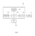
- FIG. 1 is a circuit diagram of a light radiation system in accordance with this embodiment.
- FIG. 2 is a function block diagram of a control part in this embodiment.
- FIGS. 3A and 3B are tables is a view showing determination data in this embodiment.
- FIG. 4 is an operation flow chart of the light radiation system in this embodiment.
- FIG. 5 is a circuit diagram of a light radiation system in accordance with another embodiment.
- the light radiation system 100 in accordance with this embodiment comprises, as shown in FIG. 1 , an LED light radiation device 10 as a light radiation device, and a power source device 20 to which the LED light radiation device 10 is connected, and is of, for example, a constant current type.
- the LED light radiation device 10 is connected to the power source device 20 ; however, a light radiation device that is loaded with LEDs that irradiate ultraviolet rays and that is used for UV curing may be connected to the power source device 20 .
- the LED light radiation device 10 is connected to the power source device 20 through a connector, not shown in the drawings, and comprises a light source 12 having one or a plurality of LEDs 11 and an identification resistance 13 whose resistance value is different for each type of the light source 12 .
- the light source 12 (the LED light radiation device 10 ) with specifications such as a rated current or a rated voltage, or a number or a characteristic of the LEDs 11 is different
- a different resistance value is set for the identification resistance 13 according to the type of the light source 12 in order to identify the type of the light source 12 (the LED light radiation device 10 )
- the light source 12 comprises a resistor arranged in parallel to the LEDs 11 in this embodiment.
- Eight types of the light sources 12 (the LED light radiation device 10 ) whose rated currents are different from each other are prepared in this embodiment (one of the light sources 12 is shown in FIG. 1 ), and 2.7 k ⁇ , 3.9 k ⁇ , 5.6 k ⁇ , 8.2 k ⁇ , 12 k ⁇ , 22 k ⁇ , 36 k ⁇ , and 60 k ⁇ are used for these identification resistances 13 .
- the power source device 20 is to supply an electric power to the LED light radiation device 10 to which the power source device 20 is connected, and comprises, as shown in FIG. 1 , a variable power source 21 to be connected to the light source 12 , a constant current control circuit 22 that controls the electric current supplied to the light source 12 so as to be constant, an identification resistance determination circuit 23 to determine a resistance value of the identification resistance 13 , and a control unit 24 that is connected to the identification resistance determination circuit 23 .
- the variable power source 21 is configured to apply a predetermined DC voltage to the light source 12 , and the applied voltage is set so as to flow a rated current in the light source 12 based on a voltage command value from the control unit 24 , to be described later.
- the constant current control circuit 22 performs analog control on the current flowing in the light source 12 by feedback control, and as shown concretely in FIG. 1 , is configured by making use of an operational amplifier 221 and an FET (field-effect transistor) 222 .
- the rated current of the light source 12 is input to the operational amplifier 221 as a target current by the control unit 24 , to be described later.
- the identification resistance determination circuit 23 has a voltage dividing resistance 231 connected in series to the identification resistance 13 , and is configured to divide the applied voltage of the variable power source 21 into the identification resistance 13 and the voltage dividing resistance 231 .
- the identification resistance determination circuit 23 of this embodiment comprises, as shown in FIG. 1 , a plurality of voltage dividing resistances 231 whose resistance values differ from each other, and the voltage dividing resistance 231 to be connected to the identification resistance 13 can be switched to the other voltage dividing resistance 231 . More concretely, the identification resistance determination circuit 23 is provided with a first voltage dividing resistance 231 a and a second voltage dividing resistance 231 b having a resistance larger than that of the first voltage dividing resistance 231 a in parallel, and the first voltage dividing resistance 231 a or the second voltage dividing resistance 231 b can be alternatively connected to the identification resistance 13 by the use of a switch 232 such as, for example, a semiconductor switching element.
- the resistance value of the first voltage dividing resistance 231 a is 3.3 k ⁇
- the resistance value of the second voltage dividing resistance 231 b is 15 k ⁇ .
- control unit 24 comprises a CPU, a memory, and an input device or the like, and as shown in FIG. 2 , produces functions as a divided voltage measurement part 241 , a determination data memory part 242 , a determination part 243 , and a power source control unit 244 by operating according to predetermined programs stored in the memory.
- the divided voltage measurement part 241 measures a divided voltage applied to the voltage dividing resistance 231 within a predetermined measurement range and outputs the divided voltage value to the determination part 243 , and is configured by making use of an A/D board having, for example, a predetermined resolution.
- the determination data memory part 242 is formed in a predetermined area of the memory, and stores determination data wherein information relating to the type of the light source 12 is associated with the divided voltage value measured by the divided voltage measurement part 241 .
- the applied voltage (E) of the variable power source 21 , the resistance value (R) of the identification resistance 13 , and the resistance value (r) of the voltage dividing resistance 231 are determined, the divided voltage value (V) applied to the voltage dividing resistance 231 is uniquely determined.
- the resistance value (R), (r) of each resistance 13 , 231 contains a manufacturing error, even though another different LED radiation device 10 having the light source 12 of the same type is connected to the power source device 20 , there might be a difference in the above-mentioned divided voltage value (V).
- the determination data memory part 242 of this embodiment stores the data as, for example, a lookup table by combining the resistance value of each identification resistance 13 with a predetermined range of the divided voltage value corresponding to each resistance value (hereinafter also referred to as a divided voltage value width).
- Adjacent divided voltage value widths are set not to overlap each other based on the divided voltage value (V) (a theoretical value) calculated by the above-mentioned expression (1).
- a plurality of voltage dividing resistances 231 are provided, and the determination data memory part 242 stores each of the determination data that is different for each of the voltage dividing resistances 231 .
- the determination data memory part 242 stores the first determination data corresponding to the first voltage dividing resistance 231 a and the second determination data corresponding to the second voltage dividing resistance 231 b to be combined with each voltage dividing resistance 231 .
- the determination part 243 obtains the divided voltage value from the divided voltage measurement part 241 , refers to the determination data stored in the determination data memory part 242 , and determines the type of the light source 12 that corresponds to the obtained divided voltage value.
- the determination part 243 detects which of the first voltage dividing resistance 231 a and the second voltage dividing resistance 231 b is connected to the identification resistance 13 , refers to the determination data that corresponds to the connected voltage dividing resistance 231 and determines the divided voltage value width in which the divided voltage value is contained. Then the determination part 243 determines the type of the light source 12 based on the resistance value of the identification resistance 13 corresponding to the divided voltage value width and outputs an identification signal, according to the type of the light source 12 , to the power source control unit 244 .
- the power source control unit 244 obtains the identification signal from the above-mentioned determination part 243 , and controls the variable power source 21 by outputting a control signal to the variable power source 21 in accordance with the type of the light source 12 . More concretely, the power source control unit 244 controls an electric current or a voltage of the variable power source 21 appropriately for each type of the light source 12 based on the information contained in the identification signal such as, for example, a rated current, a rated voltage, an upper limit electric current and an upper limit voltage, or the information contained in the identification signal such as a number or a characteristic of the LED 11 .
- the power source control unit 244 in this embodiment is configured to control an applied voltage of the variable power source 21 so as to flow the rated electric current in the light source 12 , and to input the rated electric current to an operational amplifier 221 of the constant current control circuit 22 as a target electric current.
- control unit 24 Next, an operation of the above-mentioned control unit 24 will be described with reference to FIG. 2 and FIG. 4 .
- the determination part 243 When the LED light radiation device 10 is connected to the power source 20 , first the determination part 243 outputs a switch signal to the switch 232 and connects the first voltage dividing resistance 231 a to the identification resistance 13 (S 1 ).
- the power source control unit 244 outputs a control signal to the variable power source 21 and applies the predetermined voltage (for example, 5V) to the identification resistance 13 , and the divided voltage measurement part 241 measures the divided voltage value of the first voltage dividing resistance 231 a (S 2 ).
- the predetermined voltage for example, 5V
- the determination part 243 obtains the divided voltage value of the first voltage dividing resistance 231 a from the divided voltage measurement part 241 , refers to the first determination data stored in the determination data memory part 242 , detects the divided voltage value width in which the divided voltage value is contained, and determines the type of the light source 12 (S 3 ).
- the determination part 243 outputs the identification signal according to the type of the determined light source 12 to the power source control unit 244 , and the power source control unit 244 controls the variable power source 21 based on the identification signal (S 5 ).
- the determination part 243 outputs the switch signal to the switch 232 and switches the voltage dividing resistance 231 to be connected to the identification resistance 13 from the first voltage dividing resistance 231 a to the second voltage dividing resistance 231 b (S 6 ).
- the divided voltage measurement part 241 measures the divided voltage value of the second voltage dividing resistance 231 b (S 7 ), and the determination part 243 refers to the second determination data stored in the determination data memory part 242 and determines the type of the light source 12 (S 8 ).
- the identification signal according to the type of the light source 12 is output to the power source control unit 244 and the power source control unit 244 controls the variable power source 21 based on the identification signal (S 10 ).
- the determination part 243 In the case that the determination part 243 is unable to determine the type of the light source 12 based on the divided voltage value of the second voltage dividing resistance 231 b (S 9 ), the determination part 243 in this embodiment outputs a signal indicating that the determination is not possible and reports the user that the type of the light source 12 is unable to be determined (S 11 ).
- the range of the resistance value of the identification resistance 13 wherein the divided voltage value can fall in the measurement range of the divided voltage measurement part 241 is changed by switching the voltage dividing resistance 231 by the determination part 243 .
- this arrangement it is possible to increase the number of the type of the light source 12 that can be determined by making use of the identification resistance 13 having a resistance value that has not been possible to use.
- the resistance value (r) of the voltage dividing resistance 231 increases by switching from the first voltage dividing resistance 231 a to the second voltage dividing resistance 231 b , even though the identification resistance 13 whose resistance value (R) is big is used, it is possible to increase the divided voltage value (V) to be measured.
- the resistance value (R) that can be used as the identification resistance 13 so that it is possible to increase the number of the types of the light source 12 that can be determined.
- the determination part 243 determines the type of the light source 12 , and the voltage dividing resistance 231 to be connected to the identification resistance 13 is configured to be switchable to the other voltage dividing resistance 231 , it is possible to automatically determine more numerous types of the light source 12 , without reducing usability for the user.
- the determination part 243 outputs the signal indicting that the determination is not possible in the case that the type of the light source 12 is unable to be determined also by the divided voltage value (V) of the second voltage dividing resistance 231 b , it is possible to notify the user that there is a defect in the LED light radiation device 10 or the power source device 20 due to deterioration of, for example, the identification resistance 13 or the voltage dividing resistance 231 , or that an LED light radiation device 10 that does not correspond to the power source device 20 is connected.
- V divided voltage value
- the identification resistance 13 and the voltage dividing resistance 231 are the resistance; however, they may be a condenser or an inductance having predetermined impedance.
- FIG. 5 it may be represented that a condenser having a different capacity for each type of the light source 12 is arranged instead of the identification resistance 13 , and a condenser having a predetermined capacity is arranged instead of the voltage dividing resistance 231 .
- the identification resistance determination circuit 23 of the above-mentioned embodiment has two voltage dividing resistances 231 ; however, it also may have an arrangement having three or more voltage dividing resistances 231 arranged in parallel.
- the light source 12 of the above-mentioned embodiment has a plurality of the LEDs 11 connected in series; however, it also may have a single LED 11 , or may have a plurality of LEDs 11 connected in parallel.
- the determination part 243 outputs the switch signal to the switch 232 and switches the voltage dividing resistance 231 ; however, it may also be so arranged that an operator inputs the switch signal from the outside and switches the voltage dividing resistance 231 .
- the power source control unit 244 of the above-mentioned embodiment is configured so that the variable power source 21 is controlled so as to flow the rated current in the light source 12 ; however, the variable power source 21 may also be controlled so as to apply the rated voltage to the light source 12 .
- the light radiation system 100 of the above-mentioned embodiment is a constant current type; however, it also may be a constant voltage type.
- the range of the resistance value that can be utilized as the identification resistance can be widened, it is possible to increase the number of the type of the light source that can be determined.
Landscapes
- Engineering & Computer Science (AREA)
- Manufacturing & Machinery (AREA)
- Led Devices (AREA)
- Circuit Arrangement For Electric Light Sources In General (AREA)
Abstract
The present invention intends to increase the type of a light source that can be determined by widening a range of an identification resistance value. The power source device is connected to a light radiation device which is equipped with: a light source having one or more LEDs; and an identification resistance whereof the resistance value differs for each type of the light source. The power source device comprises: an identification resistance determination circuit having a voltage dividing resistance connected in series to the identification resistance; and a control unit for measuring the divided voltage applied to the voltage dividing resistance, determining the type of the light source based on the divided voltage value, and controlling the power to the light source according to the type thereof. The identification resistance determination circuit has a plurality of switchable voltage dividing resistances are provided, each having a different resistance value.
Description
This invention relates to a power source device to be connected to a light radiation device and a light radiation system using the power source device.
As shown in the patent document 1, this kind of the power source device is configured to be connected to the light radiation device comprising a light source and an identification resistance whose resistance value differs for each type of the light source, and the type of the light source is automatically determined and the light source can be controlled to change the brightness of the electric light in accordance with the determined type of the light source.
If explained more concretely, the power source device has a voltage dividing resistance connected in series to the identification resistance, the divided voltage applied to the voltage dividing resistance is measured, and the type of the light source is determined based on the measured divided voltage value.
However, in the case that the type of the light source is determined based on the divided voltage value, it is necessary to select the identification resistance among a limited range of the resistance value in order for the divided voltage value to fall within the measurement range.
In addition, since the resistance value of the identification resistance contains a manufacturing error, if the resistance value of the identification resistance of each light source is close to each other, it is not possible to distinguish whether the difference in the measured divided voltage value appears due to the type of the light source or due to the manufacturing error of the identification resistance.
For this reason, the type of the resistance value that can be used as the identification resistance is limited so that the present structure can determine only limited types of the light source, and the number of these types is not satisfactory at all.
- Patent document 1: Japanese Unexamined Patent Application Publication No. 2006-351484
The present claimed invention intends to solve all of the above-mentioned problems, and a main object of this invention is to increase a number of a type of a light source that can be determined by widening a range of a resistance value of a resistance that can be used as an identification resistance.
More specifically, the power source device in accordance with this present claimed invention is a power source device that is connected to a light radiation device comprising a light source having one or a plurality of LEDs and an identification resistance whose resistance value is different for each type of the light source, and that comprises an identification resistance determination circuit that has a voltage dividing resistance to be connected to the identification resistance in series, and a control unit that measures a divided voltage applied to the voltage dividing resistance, determines the type of the light source based on the divided voltage value, and controls a power to the light source according to the type thereof, and the identification resistance determination circuit comprises a plurality of the voltage dividing resistances, each of which has a different resistance value, and is configured such that the voltage dividing resistance that is connected to the identification resistance can be switched.
In accordance with the power source device having this arrangement, since a plurality of the voltage dividing resistances whose resistance values differ from each other are switchably provided for the identification resistance determination circuit, the range of the resistance value of the identification resistance wherein the divided voltage value can fall within the measurement range is changed by switching the voltage dividing resistance. With this arrangement, it is possible to increase the number of the type of the light source that can be determined by widening the range of the resistance value of the identification resistance that can be used.
In order to make it possible to automatically determine more numerous types of the light source than that of a conventional arrangement, it is preferable that the identification resistance determination circuit comprises a first voltage dividing resistance and a second voltage dividing resistance whose resistance value is different from that of the first voltage dividing resistance, and in a case that it is not possible to determine the type of the light source based on the divided voltage applied to the first voltage dividing resistance, the control unit switches the voltage dividing resistance to be connected to the identification resistance from the first voltage dividing resistance to the second voltage dividing resistance.
In addition, in a case that it is not possible to determine the type of the light source based on the divided voltage applied to the second voltage dividing resistance, it is preferable that the control unit outputs a signal indicating that the determination is not possible.
In accordance with this arrangement, it is possible to notify a user that there is a defect in the light radiation device or the power source device due to deterioration of, for example, the identification resistance or the voltage dividing resistance, or that a light radiation device that does not correspond to the power source device is connected.
In addition, represented as a concrete embodiment is an arrangement wherein the control unit has a determination data memory part that stores determination data wherein the divided voltage value of the voltage dividing resistance is associated with information relating to the type of the light source, and the determination data memory part stores a plurality of items of the determination data, each of which corresponds to each of the voltage dividing resistances respectively in a state of being combined with each of the voltage dividing resistances.
Furthermore, a light radiation system in accordance with this invention comprises a light radiation device provided with a light source having one or a plurality of LEDs and an identification resistance whose resistance value is different for each type of the light source, and the power source device described above is connected to the light radiation device. Also in accordance with this arrangement of the light radiation system, it is possible to obtain the same effect and operation as that of the above-mentioned power source device.
In accordance with the present claimed invention having the above-mentioned arrangement, since it is possible to widen a range of the resister value that can be utilized as the identification resistance, the number of the type of the light source that can be determined can be increased.
-
- 100 . . . light radiation system
- 10 . . . LED light radiation device
- 11 . . . LED
- 12 . . . light source
- 13 . . . identification resistance
- 20 . . . power source device
- 23 . . . identification resistance determination circuit
- 231 . . . voltage dividing resistance
- 24 . . . control unit
One embodiment of a light radiation system in accordance with this invention will be described with reference to the drawings.
The light radiation system 100 in accordance with this embodiment comprises, as shown in FIG. 1 , an LED light radiation device 10 as a light radiation device, and a power source device 20 to which the LED light radiation device 10 is connected, and is of, for example, a constant current type. In this embodiment, the LED light radiation device 10 is connected to the power source device 20; however, a light radiation device that is loaded with LEDs that irradiate ultraviolet rays and that is used for UV curing may be connected to the power source device 20.
First, the LED light radiation device 10 will be described.
The LED light radiation device 10 is connected to the power source device 20 through a connector, not shown in the drawings, and comprises a light source 12 having one or a plurality of LEDs 11 and an identification resistance 13 whose resistance value is different for each type of the light source 12.
Since there are various types of the light source 12 (the LED light radiation device 10) with specifications such as a rated current or a rated voltage, or a number or a characteristic of the LEDs 11 is different, a different resistance value is set for the identification resistance 13 according to the type of the light source 12 in order to identify the type of the light source 12 (the LED light radiation device 10), and the light source 12 comprises a resistor arranged in parallel to the LEDs 11 in this embodiment.
Eight types of the light sources 12 (the LED light radiation device 10) whose rated currents are different from each other are prepared in this embodiment (one of the light sources 12 is shown in FIG. 1 ), and 2.7 kΩ, 3.9 kΩ, 5.6 kΩ, 8.2 kΩ, 12 kΩ, 22 kΩ, 36 kΩ, and 60 kΩ are used for these identification resistances 13.
Next, the power source device 20 will be described.
The power source device 20 is to supply an electric power to the LED light radiation device 10 to which the power source device 20 is connected, and comprises, as shown in FIG. 1 , a variable power source 21 to be connected to the light source 12, a constant current control circuit 22 that controls the electric current supplied to the light source 12 so as to be constant, an identification resistance determination circuit 23 to determine a resistance value of the identification resistance 13, and a control unit 24 that is connected to the identification resistance determination circuit 23.
The variable power source 21 is configured to apply a predetermined DC voltage to the light source 12, and the applied voltage is set so as to flow a rated current in the light source 12 based on a voltage command value from the control unit 24, to be described later.
The constant current control circuit 22 performs analog control on the current flowing in the light source 12 by feedback control, and as shown concretely in FIG. 1 , is configured by making use of an operational amplifier 221 and an FET (field-effect transistor) 222. The rated current of the light source 12 is input to the operational amplifier 221 as a target current by the control unit 24, to be described later.
The identification resistance determination circuit 23 has a voltage dividing resistance 231 connected in series to the identification resistance 13, and is configured to divide the applied voltage of the variable power source 21 into the identification resistance 13 and the voltage dividing resistance 231.
In the case that the applied voltage of the variable power source 21 is set to be “E”, the resistance value of the identification resistance 13 to be “R” and the resistance value of the voltage dividing resistance 231 to be “r”, a divided voltage “V” applied to the voltage dividing resistance 231 is expressed by the following expression (1).
V=E*r/(R+r) expression (1)
V=E*r/(R+r) expression (1)
The identification resistance determination circuit 23 of this embodiment comprises, as shown in FIG. 1 , a plurality of voltage dividing resistances 231 whose resistance values differ from each other, and the voltage dividing resistance 231 to be connected to the identification resistance 13 can be switched to the other voltage dividing resistance 231. More concretely, the identification resistance determination circuit 23 is provided with a first voltage dividing resistance 231 a and a second voltage dividing resistance 231 b having a resistance larger than that of the first voltage dividing resistance 231 a in parallel, and the first voltage dividing resistance 231 a or the second voltage dividing resistance 231 b can be alternatively connected to the identification resistance 13 by the use of a switch 232 such as, for example, a semiconductor switching element. In this embodiment, the resistance value of the first voltage dividing resistance 231 a is 3.3 kΩ, and the resistance value of the second voltage dividing resistance 231 b is 15 kΩ.
Physically, the control unit 24 comprises a CPU, a memory, and an input device or the like, and as shown in FIG. 2 , produces functions as a divided voltage measurement part 241, a determination data memory part 242, a determination part 243, and a power source control unit 244 by operating according to predetermined programs stored in the memory.
Each part will be described.
The divided voltage measurement part 241 measures a divided voltage applied to the voltage dividing resistance 231 within a predetermined measurement range and outputs the divided voltage value to the determination part 243, and is configured by making use of an A/D board having, for example, a predetermined resolution.
The determination data memory part 242 is formed in a predetermined area of the memory, and stores determination data wherein information relating to the type of the light source 12 is associated with the divided voltage value measured by the divided voltage measurement part 241.
More concretely explained, as is clear from the above-mentioned expression (1), if the applied voltage (E) of the variable power source 21, the resistance value (R) of the identification resistance 13, and the resistance value (r) of the voltage dividing resistance 231 are determined, the divided voltage value (V) applied to the voltage dividing resistance 231 is uniquely determined. However, practically, since the resistance value (R), (r) of each resistance 13, 231 contains a manufacturing error, even though another different LED radiation device 10 having the light source 12 of the same type is connected to the power source device 20, there might be a difference in the above-mentioned divided voltage value (V).
Then, in this embodiment, the divided voltage value corresponding to the type of each light source 12 is stored with a margin of error in consideration of the above-mentioned manufacturing error. In other words, as shown in FIGS. 3A and 3B , the determination data memory part 242 of this embodiment stores the data as, for example, a lookup table by combining the resistance value of each identification resistance 13 with a predetermined range of the divided voltage value corresponding to each resistance value (hereinafter also referred to as a divided voltage value width).
Adjacent divided voltage value widths are set not to overlap each other based on the divided voltage value (V) (a theoretical value) calculated by the above-mentioned expression (1).
In this embodiment, a plurality of voltage dividing resistances 231 are provided, and the determination data memory part 242 stores each of the determination data that is different for each of the voltage dividing resistances 231. The determination data memory part 242 stores the first determination data corresponding to the first voltage dividing resistance 231 a and the second determination data corresponding to the second voltage dividing resistance 231 b to be combined with each voltage dividing resistance 231.
The determination part 243 obtains the divided voltage value from the divided voltage measurement part 241, refers to the determination data stored in the determination data memory part 242, and determines the type of the light source 12 that corresponds to the obtained divided voltage value.
More concretely, the determination part 243 detects which of the first voltage dividing resistance 231 a and the second voltage dividing resistance 231 b is connected to the identification resistance 13, refers to the determination data that corresponds to the connected voltage dividing resistance 231 and determines the divided voltage value width in which the divided voltage value is contained. Then the determination part 243 determines the type of the light source 12 based on the resistance value of the identification resistance 13 corresponding to the divided voltage value width and outputs an identification signal, according to the type of the light source 12, to the power source control unit 244.
The power source control unit 244 obtains the identification signal from the above-mentioned determination part 243, and controls the variable power source 21 by outputting a control signal to the variable power source 21 in accordance with the type of the light source 12. More concretely, the power source control unit 244 controls an electric current or a voltage of the variable power source 21 appropriately for each type of the light source 12 based on the information contained in the identification signal such as, for example, a rated current, a rated voltage, an upper limit electric current and an upper limit voltage, or the information contained in the identification signal such as a number or a characteristic of the LED 11.
The power source control unit 244 in this embodiment is configured to control an applied voltage of the variable power source 21 so as to flow the rated electric current in the light source 12, and to input the rated electric current to an operational amplifier 221 of the constant current control circuit 22 as a target electric current.
Next, an operation of the above-mentioned control unit 24 will be described with reference to FIG. 2 and FIG. 4 .
When the LED light radiation device 10 is connected to the power source 20, first the determination part 243 outputs a switch signal to the switch 232 and connects the first voltage dividing resistance 231 a to the identification resistance 13 (S1).
Then, the power source control unit 244 outputs a control signal to the variable power source 21 and applies the predetermined voltage (for example, 5V) to the identification resistance 13, and the divided voltage measurement part 241 measures the divided voltage value of the first voltage dividing resistance 231 a (S2).
Next, the determination part 243 obtains the divided voltage value of the first voltage dividing resistance 231 a from the divided voltage measurement part 241, refers to the first determination data stored in the determination data memory part 242, detects the divided voltage value width in which the divided voltage value is contained, and determines the type of the light source 12 (S3).
In the case that the divided voltage value width in which the divided voltage value is contained is detected (S4), the determination part 243 outputs the identification signal according to the type of the determined light source 12 to the power source control unit 244, and the power source control unit 244 controls the variable power source 21 based on the identification signal (S5).
Meanwhile, in the case that the determination part 243 is unable to determine the type of the light source 12 based on the divided voltage value of the first voltage dividing resistance 231 a, namely, in the case that the divided voltage value measured by the divided voltage measurement part 241 is not contained in any divided voltage value width (S4), the determination part 243 outputs the switch signal to the switch 232 and switches the voltage dividing resistance 231 to be connected to the identification resistance 13 from the first voltage dividing resistance 231 a to the second voltage dividing resistance 231 b (S6).
Similar to the case wherein the type of the light source 12 is determined by the use of the first voltage dividing resistance 231 a, the divided voltage measurement part 241 measures the divided voltage value of the second voltage dividing resistance 231 b (S7), and the determination part 243 refers to the second determination data stored in the determination data memory part 242 and determines the type of the light source 12 (S8).
In the case that the type of the light source 12 is determined (S9), the identification signal according to the type of the light source 12 is output to the power source control unit 244 and the power source control unit 244 controls the variable power source 21 based on the identification signal (S10).
In the case that the determination part 243 is unable to determine the type of the light source 12 based on the divided voltage value of the second voltage dividing resistance 231 b (S9), the determination part 243 in this embodiment outputs a signal indicating that the determination is not possible and reports the user that the type of the light source 12 is unable to be determined (S11).
In accordance with the light radiation system 100 of this embodiment having the above-mentioned arrangement, since a plurality of voltage dividing resistances 231 whose resistance values differ from each other are switchably provided for the identification resistance determination circuit 23, the range of the resistance value of the identification resistance 13 wherein the divided voltage value can fall in the measurement range of the divided voltage measurement part 241 is changed by switching the voltage dividing resistance 231 by the determination part 243. With this arrangement, it is possible to increase the number of the type of the light source 12 that can be determined by making use of the identification resistance 13 having a resistance value that has not been possible to use.
As is clear from the above-mentioned expression (1), in the case that the resistance value (R) of the identification resistance 13 is big, the measured divided voltage value (V) becomes a value close to zero.
According to this, conventionally, when the difference in the measured divided voltage value at a time when a certain identification resistance 13 is changed to another identification resistance 13 becomes smaller than the resolution of the measurement part, it is not possible to distinguish the two different identification resistances 13, and thus it is difficult to use the identification resistance 13 having a large resistance value (R), also resulting in limiting the types of the light source 12 that can be determined.
Meanwhile, in accordance with the light radiation system 100 of this invention, since the resistance value (r) of the voltage dividing resistance 231 increases by switching from the first voltage dividing resistance 231 a to the second voltage dividing resistance 231 b, even though the identification resistance 13 whose resistance value (R) is big is used, it is possible to increase the divided voltage value (V) to be measured. With this arrangement, it is possible to widen the range of the resistance value (R) that can be used as the identification resistance 13 so that it is possible to increase the number of the types of the light source 12 that can be determined.
Furthermore, since the determination part 243 determines the type of the light source 12, and the voltage dividing resistance 231 to be connected to the identification resistance 13 is configured to be switchable to the other voltage dividing resistance 231, it is possible to automatically determine more numerous types of the light source 12, without reducing usability for the user.
In addition, since the determination part 243 outputs the signal indicting that the determination is not possible in the case that the type of the light source 12 is unable to be determined also by the divided voltage value (V) of the second voltage dividing resistance 231 b, it is possible to notify the user that there is a defect in the LED light radiation device 10 or the power source device 20 due to deterioration of, for example, the identification resistance 13 or the voltage dividing resistance 231, or that an LED light radiation device 10 that does not correspond to the power source device 20 is connected.
The present claimed invention is not limited to the above-mentioned embodiments.
In the above-mentioned embodiments, for example, the identification resistance 13 and the voltage dividing resistance 231 are the resistance; however, they may be a condenser or an inductance having predetermined impedance.
As a concrete embodiment, as shown in FIG. 5 , it may be represented that a condenser having a different capacity for each type of the light source 12 is arranged instead of the identification resistance 13, and a condenser having a predetermined capacity is arranged instead of the voltage dividing resistance 231.
The identification resistance determination circuit 23 of the above-mentioned embodiment has two voltage dividing resistances 231; however, it also may have an arrangement having three or more voltage dividing resistances 231 arranged in parallel.
The light source 12 of the above-mentioned embodiment has a plurality of the LEDs 11 connected in series; however, it also may have a single LED 11, or may have a plurality of LEDs 11 connected in parallel.
In the above-mentioned embodiment, the determination part 243 outputs the switch signal to the switch 232 and switches the voltage dividing resistance 231; however, it may also be so arranged that an operator inputs the switch signal from the outside and switches the voltage dividing resistance 231.
The power source control unit 244 of the above-mentioned embodiment is configured so that the variable power source 21 is controlled so as to flow the rated current in the light source 12; however, the variable power source 21 may also be controlled so as to apply the rated voltage to the light source 12.
The light radiation system 100 of the above-mentioned embodiment is a constant current type; however, it also may be a constant voltage type.
In addition, the present claimed invention is not limited to the above-mentioned embodiments, and may be variously modified without departing from the spirit of the invention.
As mentioned above, in accordance with the present claimed invention, since the range of the resistance value that can be utilized as the identification resistance can be widened, it is possible to increase the number of the type of the light source that can be determined.
Claims (5)
1. A power source device that is connected to a light radiation device comprising a light source having one or a plurality of LEDs and an identification resistance whose resistance value is different for each type of the light source, comprising:
an identification resistance determination circuit that has a voltage dividing resistance to be connected to the identification resistance in series; and
a control unit that measures a divided voltage applied to the voltage dividing resistance, determines the type of the light source based on the divided voltage value, and controls a power to the light source according to the type thereof, wherein
the identification resistance determination circuit comprises a plurality of the voltage dividing resistances each of which has a different resistance value, and is configured such that the voltage dividing resistance that is connected to the identification resistance can be switched.
2. The power source device described in claim 1 , wherein
the identification resistance determination circuit comprises a first voltage dividing resistance and a second voltage dividing resistance whose resistance value is different from that of the first voltage dividing resistance, and
in a case that it is not possible to determine the type of the light source based on the divided voltage applied to the first voltage dividing resistance, the control unit switches the voltage dividing resistance to be connected to the identification resistance from the first voltage dividing resistance to the second voltage dividing resistance.
3. The power source device described in claim 2 , wherein
in a case that it is not possible to determine the type of the light source based on the divided voltage applied to the second voltage dividing resistance, the control unit outputs a signal indicating that the determination is not possible.
4. The power source device described in claim 1 , wherein
the control unit has a determination data memory part that stores determination data wherein the divided voltage value of the voltage dividing resistance is associated with information relating to the type of the light source, and
the determination data memory part stores a plurality of items of determination data, each of which corresponds to each of the voltage dividing resistances respectively in a state of being combined with each of the voltage dividing resistances.
5. A light radiation system, comprising:
a light radiation device provided with a light source having one or a plurality of LEDs and an identification resistance whose resistance value is different for each type of the light source, and
the power source device described in claim 1 , connected to the light radiation device.
Applications Claiming Priority (3)
| Application Number | Priority Date | Filing Date | Title |
|---|---|---|---|
| JP2015136605A JP6654367B2 (en) | 2015-07-08 | 2015-07-08 | Power supply device and light irradiation system including the same |
| JP2015-136605 | 2015-07-08 | ||
| PCT/JP2016/067517 WO2017006709A1 (en) | 2015-07-08 | 2016-06-13 | Power source device and light radiation system equipped with same |
Publications (2)
| Publication Number | Publication Date |
|---|---|
| US20180192489A1 US20180192489A1 (en) | 2018-07-05 |
| US10028346B1 true US10028346B1 (en) | 2018-07-17 |
Family
ID=57685098
Family Applications (1)
| Application Number | Title | Priority Date | Filing Date |
|---|---|---|---|
| US15/741,032 Active US10028346B1 (en) | 2015-07-08 | 2016-06-13 | Power source device and light radiation system equipped with same |
Country Status (5)
| Country | Link |
|---|---|
| US (1) | US10028346B1 (en) |
| EP (1) | EP3321981B1 (en) |
| JP (1) | JP6654367B2 (en) |
| CN (1) | CN107851686B (en) |
| WO (1) | WO2017006709A1 (en) |
Families Citing this family (7)
| Publication number | Priority date | Publication date | Assignee | Title |
|---|---|---|---|---|
| CN106376142B (en) * | 2016-10-31 | 2020-04-28 | 恒亦明(重庆)科技有限公司 | Load with identification and power output parameter self-adjusting system |
| TWI674815B (en) * | 2018-10-01 | 2019-10-11 | 龍華科技大學 | An adaptive LED driver |
| TWI703897B (en) * | 2019-05-07 | 2020-09-01 | 益力半導體股份有限公司 | Self-adaptive dimming drive system |
| CN110366291B (en) * | 2019-07-05 | 2024-04-09 | 欧普照明股份有限公司 | Power supply driving and lamp automatically matched with loads of light sources with multiple specifications and driving method |
| CN110461056B (en) * | 2019-07-05 | 2024-04-09 | 欧普照明股份有限公司 | Power supply driving, lamp and driving method capable of automatically matching loads of multiple light sources |
| GB2613141A (en) * | 2021-10-01 | 2023-05-31 | Simmtronic Ltd | Lighting system |
| CN114267269B (en) * | 2022-01-11 | 2023-07-21 | 福州不止光电科技有限公司 | Free-mounting free combined type luminous sign |
Citations (11)
| Publication number | Priority date | Publication date | Assignee | Title |
|---|---|---|---|---|
| JPH07297793A (en) | 1994-04-28 | 1995-11-10 | Kokusai Electric Co Ltd | Sound volume level adjusting device |
| JP2001024226A (en) | 1999-07-07 | 2001-01-26 | Nec Saitama Ltd | Light emitting diode and displaying circuit using the same |
| US20040090189A1 (en) * | 2002-10-16 | 2004-05-13 | Kenji Yoneda | Electric power supply system for LED lighting unit |
| JP2004158840A (en) | 2002-10-16 | 2004-06-03 | Ccs Inc | Power supply system for led lighting devices |
| JP2006351484A (en) | 2005-06-20 | 2006-12-28 | Moritex Corp | Illumination device and illumination head used for the same |
| JP2011138716A (en) | 2009-12-29 | 2011-07-14 | Mitsubishi Electric Corp | Power supply unit, light source unit, lighting device and display device |
| JP2013004280A (en) | 2011-06-15 | 2013-01-07 | Panasonic Corp | Light emitting device and illuminating device |
| JP2013136298A (en) | 2011-12-28 | 2013-07-11 | Denso Corp | Light emission driver device |
| JP2014030358A (en) | 2013-11-14 | 2014-02-13 | Lenovo Singapore Pte Ltd | Battery unit for supplying power to electric/electronic apparatuses and method for supplying power |
| US20150373811A1 (en) * | 2012-12-21 | 2015-12-24 | Tridonic Gmbh & Co Kg | Detection of an led module |
| US20160021712A1 (en) * | 2014-07-15 | 2016-01-21 | Panasonic Intellectual Property Management Co., Ltd. | Lighting device, light source device, illuminating device, and vehicular headlight |
Family Cites Families (4)
| Publication number | Priority date | Publication date | Assignee | Title |
|---|---|---|---|---|
| JPS58106470A (en) * | 1981-12-18 | 1983-06-24 | Nec Corp | High resistance measuring device |
| JPS61184967U (en) * | 1985-05-09 | 1986-11-18 | ||
| JP2011238380A (en) * | 2010-05-06 | 2011-11-24 | Ccs Inc | Power supply and discrimination circuit |
| JP6278350B2 (en) * | 2014-01-14 | 2018-02-14 | アール・ビー・コントロールズ株式会社 | LED lighting device |
-
2015
- 2015-07-08 JP JP2015136605A patent/JP6654367B2/en active Active
-
2016
- 2016-06-13 EP EP16821179.5A patent/EP3321981B1/en active Active
- 2016-06-13 WO PCT/JP2016/067517 patent/WO2017006709A1/en active Application Filing
- 2016-06-13 US US15/741,032 patent/US10028346B1/en active Active
- 2016-06-13 CN CN201680040077.9A patent/CN107851686B/en active Active
Patent Citations (11)
| Publication number | Priority date | Publication date | Assignee | Title |
|---|---|---|---|---|
| JPH07297793A (en) | 1994-04-28 | 1995-11-10 | Kokusai Electric Co Ltd | Sound volume level adjusting device |
| JP2001024226A (en) | 1999-07-07 | 2001-01-26 | Nec Saitama Ltd | Light emitting diode and displaying circuit using the same |
| US20040090189A1 (en) * | 2002-10-16 | 2004-05-13 | Kenji Yoneda | Electric power supply system for LED lighting unit |
| JP2004158840A (en) | 2002-10-16 | 2004-06-03 | Ccs Inc | Power supply system for led lighting devices |
| JP2006351484A (en) | 2005-06-20 | 2006-12-28 | Moritex Corp | Illumination device and illumination head used for the same |
| JP2011138716A (en) | 2009-12-29 | 2011-07-14 | Mitsubishi Electric Corp | Power supply unit, light source unit, lighting device and display device |
| JP2013004280A (en) | 2011-06-15 | 2013-01-07 | Panasonic Corp | Light emitting device and illuminating device |
| JP2013136298A (en) | 2011-12-28 | 2013-07-11 | Denso Corp | Light emission driver device |
| US20150373811A1 (en) * | 2012-12-21 | 2015-12-24 | Tridonic Gmbh & Co Kg | Detection of an led module |
| JP2014030358A (en) | 2013-11-14 | 2014-02-13 | Lenovo Singapore Pte Ltd | Battery unit for supplying power to electric/electronic apparatuses and method for supplying power |
| US20160021712A1 (en) * | 2014-07-15 | 2016-01-21 | Panasonic Intellectual Property Management Co., Ltd. | Lighting device, light source device, illuminating device, and vehicular headlight |
Non-Patent Citations (1)
| Title |
|---|
| ISA Japan Patent Office, International Search Report Issued in PCT Application No. PCT/JP2016/067517, dated Aug. 30, 2016, WIPO, 4 pages. (Submitted with English Translation of International Search Report). |
Also Published As
| Publication number | Publication date |
|---|---|
| EP3321981A4 (en) | 2019-01-16 |
| CN107851686B (en) | 2019-08-09 |
| EP3321981B1 (en) | 2020-07-29 |
| WO2017006709A1 (en) | 2017-01-12 |
| JP6654367B2 (en) | 2020-02-26 |
| CN107851686A (en) | 2018-03-27 |
| US20180192489A1 (en) | 2018-07-05 |
| EP3321981A1 (en) | 2018-05-16 |
| JP2017022193A (en) | 2017-01-26 |
Similar Documents
| Publication | Publication Date | Title |
|---|---|---|
| US10028346B1 (en) | Power source device and light radiation system equipped with same | |
| US9385613B2 (en) | Method of operating switch mode power converters, and controllers and lighting systems using such a method | |
| US10261137B2 (en) | Magnetic sensor | |
| US20170328786A1 (en) | Temperature detecting apparatus | |
| JP2007502569A (en) | Operation and circuit of power conversion circuit and power control circuit | |
| US20120056544A1 (en) | Apparatus for driving light emitting device | |
| US11372026B2 (en) | Resistance measuring device and method | |
| WO2017037780A1 (en) | Power conversion device and semiconductor device | |
| JP6263272B2 (en) | Current detection apparatus and method for detecting current | |
| RU2014148781A (en) | SHIFT COMPENSATION IN EXCITATION SCHEMES | |
| US20160124525A1 (en) | Amending Circuit Capable of Switching Mouse into Different Detecting Modes | |
| KR101493213B1 (en) | Apparatus for distinguishing type of analog sensor | |
| US20110234301A1 (en) | Circuit arrangement with temperature compensation | |
| US7355372B2 (en) | Power control system capable of balancing output currents | |
| US20180335469A1 (en) | Drive circuit for insulated-gate semiconductor element | |
| US7639468B2 (en) | Circuit for load current measurement, limitation and switching | |
| US10390403B2 (en) | Power supply device used for LED light output device | |
| KR100979835B1 (en) | Constant Current Driver for LED Lighting System | |
| US20230010478A1 (en) | Power device | |
| JP6271285B2 (en) | Semiconductor test equipment | |
| KR102108344B1 (en) | Circuit and method for detecting short circuit in LED lamp | |
| JP7247580B2 (en) | UV irradiation device | |
| KR101855731B1 (en) | Portable LED Lighting Device | |
| JP7278171B2 (en) | LED burn-out detection mechanism and LED light irradiation system using the same | |
| JP6539100B2 (en) | Power supply control device for vehicle |
Legal Events
| Date | Code | Title | Description |
|---|---|---|---|
| FEPP | Fee payment procedure |
Free format text: ENTITY STATUS SET TO UNDISCOUNTED (ORIGINAL EVENT CODE: BIG.); ENTITY STATUS OF PATENT OWNER: LARGE ENTITY |
|
| STCF | Information on status: patent grant |
Free format text: PATENTED CASE |
|
| MAFP | Maintenance fee payment |
Free format text: PAYMENT OF MAINTENANCE FEE, 4TH YEAR, LARGE ENTITY (ORIGINAL EVENT CODE: M1551); ENTITY STATUS OF PATENT OWNER: LARGE ENTITY Year of fee payment: 4 |