EP3319310A1 - Solid-state imaging device - Google Patents
Solid-state imaging device Download PDFInfo
- Publication number
- EP3319310A1 EP3319310A1 EP16817838.2A EP16817838A EP3319310A1 EP 3319310 A1 EP3319310 A1 EP 3319310A1 EP 16817838 A EP16817838 A EP 16817838A EP 3319310 A1 EP3319310 A1 EP 3319310A1
- Authority
- EP
- European Patent Office
- Prior art keywords
- charge
- capacitance portion
- pixels
- imaging device
- solid
- Prior art date
- Legal status (The legal status is an assumption and is not a legal conclusion. Google has not performed a legal analysis and makes no representation as to the accuracy of the status listed.)
- Granted
Links
Images






Classifications
-
- G—PHYSICS
- G01—MEASURING; TESTING
- G01T—MEASUREMENT OF NUCLEAR OR X-RADIATION
- G01T1/00—Measuring X-radiation, gamma radiation, corpuscular radiation, or cosmic radiation
- G01T1/16—Measuring radiation intensity
- G01T1/20—Measuring radiation intensity with scintillation detectors
-
- H—ELECTRICITY
- H04—ELECTRIC COMMUNICATION TECHNIQUE
- H04N—PICTORIAL COMMUNICATION, e.g. TELEVISION
- H04N25/00—Circuitry of solid-state image sensors [SSIS]; Control thereof
- H04N25/30—Circuitry of solid-state image sensors [SSIS]; Control thereof for transforming X-rays into image signals
-
- H—ELECTRICITY
- H04—ELECTRIC COMMUNICATION TECHNIQUE
- H04N—PICTORIAL COMMUNICATION, e.g. TELEVISION
- H04N25/00—Circuitry of solid-state image sensors [SSIS]; Control thereof
- H04N25/40—Extracting pixel data from image sensors by controlling scanning circuits, e.g. by modifying the number of pixels sampled or to be sampled
-
- H—ELECTRICITY
- H04—ELECTRIC COMMUNICATION TECHNIQUE
- H04N—PICTORIAL COMMUNICATION, e.g. TELEVISION
- H04N25/00—Circuitry of solid-state image sensors [SSIS]; Control thereof
- H04N25/60—Noise processing, e.g. detecting, correcting, reducing or removing noise
-
- H—ELECTRICITY
- H04—ELECTRIC COMMUNICATION TECHNIQUE
- H04N—PICTORIAL COMMUNICATION, e.g. TELEVISION
- H04N25/00—Circuitry of solid-state image sensors [SSIS]; Control thereof
- H04N25/60—Noise processing, e.g. detecting, correcting, reducing or removing noise
- H04N25/62—Detection or reduction of noise due to excess charges produced by the exposure, e.g. smear, blooming, ghost image, crosstalk or leakage between pixels
- H04N25/626—Reduction of noise due to residual charges remaining after image readout, e.g. to remove ghost images or afterimages
-
- H—ELECTRICITY
- H04—ELECTRIC COMMUNICATION TECHNIQUE
- H04N—PICTORIAL COMMUNICATION, e.g. TELEVISION
- H04N25/00—Circuitry of solid-state image sensors [SSIS]; Control thereof
- H04N25/70—SSIS architectures; Circuits associated therewith
- H04N25/71—Charge-coupled device [CCD] sensors; Charge-transfer registers specially adapted for CCD sensors
-
- H—ELECTRICITY
- H04—ELECTRIC COMMUNICATION TECHNIQUE
- H04N—PICTORIAL COMMUNICATION, e.g. TELEVISION
- H04N25/00—Circuitry of solid-state image sensors [SSIS]; Control thereof
- H04N25/70—SSIS architectures; Circuits associated therewith
- H04N25/76—Addressed sensors, e.g. MOS or CMOS sensors
-
- H—ELECTRICITY
- H04—ELECTRIC COMMUNICATION TECHNIQUE
- H04N—PICTORIAL COMMUNICATION, e.g. TELEVISION
- H04N25/00—Circuitry of solid-state image sensors [SSIS]; Control thereof
- H04N25/70—SSIS architectures; Circuits associated therewith
- H04N25/76—Addressed sensors, e.g. MOS or CMOS sensors
- H04N25/78—Readout circuits for addressed sensors, e.g. output amplifiers or A/D converters
-
- H—ELECTRICITY
- H10—SEMICONDUCTOR DEVICES; ELECTRIC SOLID-STATE DEVICES NOT OTHERWISE PROVIDED FOR
- H10F—INORGANIC SEMICONDUCTOR DEVICES SENSITIVE TO INFRARED RADIATION, LIGHT, ELECTROMAGNETIC RADIATION OF SHORTER WAVELENGTH OR CORPUSCULAR RADIATION
- H10F39/00—Integrated devices, or assemblies of multiple devices, comprising at least one element covered by group H10F30/00, e.g. radiation detectors comprising photodiode arrays
- H10F39/10—Integrated devices
- H10F39/12—Image sensors
-
- H—ELECTRICITY
- H10—SEMICONDUCTOR DEVICES; ELECTRIC SOLID-STATE DEVICES NOT OTHERWISE PROVIDED FOR
- H10F—INORGANIC SEMICONDUCTOR DEVICES SENSITIVE TO INFRARED RADIATION, LIGHT, ELECTROMAGNETIC RADIATION OF SHORTER WAVELENGTH OR CORPUSCULAR RADIATION
- H10F99/00—Subject matter not provided for in other groups of this subclass
Definitions
- the present invention relates to a solid-state imaging device.
- a solid-state imaging device includes a photodetecting unit having a plurality of pixels on a principal surface of a semiconductor substrate, and a signal readout unit that reads out a charge from each of the plurality of pixels and outputs a signal value according to an amount of charge (see Patent Documents 1 to 5).
- Each of the plurality of pixels includes a photodiode that generates a charge according to light incidence.
- the signal readout unit includes an integration circuit in which an integration capacitance portion is provided between an input terminal and an output terminal of an amplifier, accumulates a charge generated in the photodiode of each pixel in the integration capacitance portion, and outputs a signal value according to an amount of accumulated charge.
- a solid-state imaging device described in Patent Document 1 includes an integration circuit common to a plurality of pixels.
- a solid-state imaging device having such a configuration accumulates a charge generated in a photodiode according to light incidence in each of a plurality of pixels in a junction capacitance portion of the photodiode, sequentially transfers the charge accumulated in the junction capacitance portion of the photodiode of each pixel to an integration capacitance portion of the common integration circuit, and outputs a signal value according to an amount of charge from the integration circuit.
- a buried photodiode may be used as the photodiode of each pixel.
- junction capacitance decreases, an output voltage changes linearly with respect to an amount of accumulated charge, and a charge generated in a pn junction portion can be almost completely read out such that the S/N ratio and linearity in light detection are excellent.
- the buried photodiode has higher resistance than a normal photodiode.
- an area of a light detection region of a photodiode of a solid-state imaging device in medical applications is about 100 times that of a usual application (for example, for capturing an optical image in a digital camera).
- a charge readout time from the junction capacitance portion of the photodiode is lengthened.
- the present invention has been made in order to solve the above problem, and an object thereof is to provide a solid-state imaging device which can shorten a charge readout time from a junction capacitance portion of a photodiode of each pixel and which has an excellent S/N ratio and linearity in light detection.
- a solid-state imaging device includes a photodetecting unit including a plurality of pixels on a first principal surface of a semiconductor substrate having the first principal surface and a second principal surface opposite to each other; a signal readout unit outputting a signal value according to an amount of charge output from each of the plurality of pixels; and a control unit controlling an operation of each of the photodetecting unit and the signal readout unit.
- each of the plurality of pixels includes a plurality of buried photodiodes each of which generates a charge according to light incidence and accumulates the charge in a junction capacitance portion; a capacitance portion accumulating the charge transferred from the junction capacitance portion of each of the plurality of photodiodes; a transfer switch group for transferring the charge from the junction capacitance portion of each of the plurality of photodiodes to the capacitance portion; and an output switch for outputting the charge from the capacitance portion to the signal readout unit.
- control unit controls so as to accumulate the charge generated according to the light incidence in each of the plurality of pixels in the junction capacitance portion of each photodiode during a common charge accumulation period, transfer the charge from the junction capacitance portion of each photodiode to the capacitance portion by setting the transfer switch group to an ON state in each of the plurality of pixels after the charge accumulation period, and output the charge from the capacitance portion to the signal readout unit by sequentially setting the output switch to an ON state in each of the plurality of pixels after charge transfer.
- a solid-state imaging device which can shorten a charge readout time from a junction capacitance portion of a photodiode of each pixel and which has an excellent S/N ratio and linearity in light detection.
- FIG. 1 is an entire configuration diagram of a solid-state imaging device 1 of the first embodiment.
- the solid-state imaging device 1 includes a photodetecting unit 10 and a signal readout unit 20, and further includes a control unit 30 that controls respective operations of the photodetecting unit 10 and the signal readout unit 20.
- the photodetecting unit 10 has M ⁇ N pixels P 1,1 to P M,N on a first principal surface of a semiconductor substrate having the first principal surface and a second principal surface opposite to each other.
- the M ⁇ N pixels P 1,1 to P M,N have a common configuration and are arrayed two-dimensionally.
- a pixel P m,n is located in an m-th row and an n-th column.
- Each pixel P m,n includes a photodiode that generates a charge according to light incidence and can output the charge.
- M and N are each an integer of 2 or more.
- m is an integer of 1 or more and M or less.
- n is an integer of 1 or more and N or less.
- the signal readout unit 20 outputs a signal value according to an amount of charge output from each of the M ⁇ N pixels P 1,1 to P M,N .
- the signal readout unit 20 includes N integration circuits 21 1 to 21 N , N hold circuits 22 1 to 22 N , and an AD conversion circuit 23.
- the N integration circuits 21 1 to 21 N have a common configuration.
- the N hold circuits 22 1 to 22 N have a common configuration.
- the n-th integration circuit 21 n inputs the charge sequentially output from each of the M pixels P 1,n to P M,n of the n-th column, and outputs a voltage value according to the amount of charge to the hold circuit 22 n .
- the n-th hold circuit 22 n inputs and holds the voltage value output from the integration circuit 21 n .
- the N hold circuits 22 1 to 22 N sequentially output voltage values held thereby to the AD conversion circuit 23.
- the AD conversion circuit 23 inputs a voltage value sequentially output from each of the N hold circuits 22 1 to 22 N , converts the input voltage value into a digital value, and outputs the digital value.
- the digital value output from the AD conversion circuit 23 is a signal value according to an amount of charge output from each of the M ⁇ N pixels P 1,1 to P M,N .
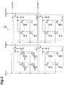
- FIG. 2 is a circuit diagram of the pixel P m,n and the integration circuit 21 n of the solid-state imaging device 1 of the first embodiment.
- FIG. 2 illustrates two pixels P m,n and P m+1,n of the n-th column as representatives of the M ⁇ N pixels P 1,1 to P M,N , and illustrates the n-th integration circuit 21 n as a representative of the N integration circuits 21 1 to 21 N .
- Each pixel P m,n includes a plurality of buried photodiodes PD, a capacitance portion C 1 , a plurality of transfer switches SW 1 , and an output switch SW 2 .
- Each of the transfer switches SW 1 and the output switch SW 2 may be configured by a MOS transistor.
- Each photodiode PD can generate a charge according to the light incidence and accumulate the charge in a junction capacitance portion.
- the capacitance portion C 1 accumulates the charge transferred from the junction capacitance portion of each of the plurality of photodiodes PD via the transfer switch SW 1 .
- one capacitance portion C 1 may be provided or a plurality of partial capacitance portions may be provided in parallel.
- Each transfer switch SW 1 is provided in a one-to-one correspondence with the photodiode PD. Each pair of the photodiode PD and the transfer switch SW 1 is provided in parallel to the capacitance portion C 1 . Each transfer switch SW 1 can transfer the charge from the junction capacitance portion of the photodiode PD to the capacitance portion C 1 in an ON state. The output switch SW 2 can output the charge from the capacitance portion C 1 to the integration circuit 21 n of the signal readout unit 20 in an ON state.
- Each integration circuit 21 n includes an amplifier A 21 , a capacitance portion C 21 , and an initialization switch SW 21 .
- the capacitance portion C 21 and the initialization switch SW 21 are connected in parallel and are provided between an input terminal and an output terminal of the amplifier A 21 .
- the initialization switch SW 21 may be configured by a MOS transistor. When the initialization switch SW 21 is in an ON state, charge accumulation in the capacitance portion C 21 is initialized. When the initialization switch SW 21 is in an OFF state, the capacitance portion C 21 can accumulate the input charge.
- the integration circuit 21 n outputs a voltage value according to the amount of accumulated charge in the capacitance portion C 21 .
- An ON/OFF operation of the transfer switch SW 1 of each pixel P m,n is controlled by a control signal ⁇ tran output from the control unit 30.
- An ON/OFF operation of the output switch SW 2 of each pixel P m,n is controlled by a control signal ⁇ sel(m) output from the control unit 30.
- An ON/OFF operation of the initialization switch SW 21 of each integration circuit 21 n is controlled by a control signal ⁇ reset output from the control unit 30.
- FIG. 3 is a circuit diagram of the pixel P m,n , the pixel P m+1,n , a pixel P m,n+1 , and a pixel P m+1,n+1 of the solid-state imaging device 1 of the first embodiment.
- FIG. 3 illustrates pixels of two rows and two columns as representatives of M rows and N columns.
- the control unit 30 applies the common control signal ⁇ tran to the M ⁇ N pixels P 1,1 to P M,N .
- the control signal ⁇ tran is a signal for controlling the ON/OFF operations of the transfer switches SW 1 of all of the pixels.
- the control unit 30 applies the common control signal ⁇ sel(m) to the N pixels P m,1 to P m,N of the m-th row.
- the control signal ⁇ sel(m) is a signal for controlling the ON/OFF operations of the output switches SW 2 of the N pixels of the m-th row. A period in which the output switch SW 2 is in the ON state according to the control signal is different in the first to M-th rows.
- the n-th integration circuit 21 n inputs a charge signal out(n) sequentially output from the output switch SW 2 of each of the M pixels P 1,n to P M,n of the n-th column.
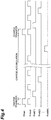
- FIG. 4 is a timing chart illustrating an example of an operation of the solid-state imaging device 1 of the first embodiment.
- FIG. 4 illustrates the control signal ⁇ tran to be applied to the transfer switch SW 1 of each pixel P m,n , the control signal ⁇ reset to be applied to the initialization switch SW 21 of each integration circuit 21 n , and the control signals ⁇ sel(1) to ⁇ sel(M) to be applied to the output switch SW 2 of the pixel P m,n of each row.
- Each switch is assumed to be in the ON state when the applied control signal has a high level.
- the control signal ⁇ tran has the high level in a constant cycle, and the transfer switches SW 1 of all of the pixels alternately repeat the ON state period and the OFF state period in a constant cycle.
- the transfer switches SW 1 are in the OFF state in all of the pixels, and the charge generated according to the light incidence on each photodiode PD is accumulated in the junction capacitance portion of the photodiode PD.
- the transfer switches SW 1 are in the ON state in all of the pixels, and further, the control signals ⁇ sel(1) to ⁇ sel(M) have the low level, and the output switches SW 2 are in the OFF state in all of the pixels.
- the charge accumulated until then in the junction capacitance portion of each photodiode PD is transferred to the capacitance portion C 1 via the transfer switch SW 1 .
- the control signal ⁇ reset has the high level in the period in which the control signal ⁇ tran has the high level, and the control signal ⁇ reset also has the high level at a constant interval in a subsequent period (charge accumulation period) in which the control signal ⁇ tran has the low level.
- the initialization switch SW 21 is in the ON state in each of the N integration circuits 21 1 to 21 N , and the charge accumulation in the capacitance portion C 21 is initialized.
- any one control signal ⁇ sel(m) of the control signals ⁇ sel(1) to ⁇ sel(M) has the high level in the period in which the control signal ⁇ reset has the low level.
- the output switch SW 2 is in the ON state in each of the N pixels P m,1 to P m,N of the m-th row to which the control signal ⁇ sel(m) having the high level is applied, and the charge accumulated in the capacitance portion C 1 is output as the charge signal out(n).
- the charge signal out(n) is input to the n-th integration circuit 21 n and accumulated in the capacitance portion C 21 , and a voltage value according to the amount of accumulated charge is output from the integration circuit 21 n .
- control unit 30 causes the charge generated according to the light incidence to be accumulated in the junction capacitance portion of each photodiode PD in all of the pixels during the common charge accumulation period. After the charge accumulation period, the control unit 30 causes the charge to be transferred from the junction capacitance portion of each photodiode PD to the capacitance portion C 1 by setting the transfer switches SW 1 to the ON state in all of the pixels. Then, after the charge is transferred, the control unit 30 causes the charge to be output from the capacitance portion C 1 to the signal readout unit 20 by sequentially setting the output switches SW 2 to the ON state for respective rows. The control unit 30 can cause the charge to be output from the capacitance portion C 1 of each pixel to the signal readout unit 20 in the charge accumulation period in which the charge is accumulated in the junction capacitance portion of each photodiode PD.
- FIG. 5 is a diagram illustrating an example of a cross-sectional structure of the photodetecting unit 10 of the solid-state imaging device 1 of the first embodiment.
- FIG. 5 schematically illustrates an example of a cross-sectional structure of the two pixels P m,n and P m+1,n of the n-th column as representatives of the M ⁇ N pixels P 1,1 to P M,N . Further, in FIG. 5 , the number of photodiodes PD of each pixel P m,n is assumed to be 2.
- the photodetecting unit 10 includes a p-type first semiconductor region 101, an n - -type second semiconductor region 102, a p + -type third semiconductor region 103, an n + -type fourth semiconductor region 104, an n + -type fifth semiconductor region 105, an insulator layer 107, gate electrodes 111 and 112, a first conductor layer 121, a second conductor layer 122, an insulator layer 123, and electrode pads 131 to 133, formed on the first principal surface (an upper surface in FIG. 5 ) of the semiconductor substrate 100.
- the p-type first semiconductor region 101 is widely formed on the first principal surface of the semiconductor substrate 100.
- the n - -type second semiconductor region 102 is formed on a partial range of the p-type first semiconductor region 101.
- the p + -type third semiconductor region 103 is formed on both the p-type first semiconductor region 101 and the n - -type second semiconductor region 102.
- Each of the n + -type fourth semiconductor region 104 and the n + -type fifth semiconductor region 105 is formed on the p-type first semiconductor region 101.
- the insulator layer 107 is formed on substantially the entire semiconductor regions except a part thereof.
- the gate electrode 111 is provided above the p-type first semiconductor region 101 between the n - -type second semiconductor region 102 and the n + -type fourth semiconductor region 104, and is formed on the insulator layer 107.
- the gate electrode 112 is provided above the p-type first semiconductor region 101 between the n + -type fourth semiconductor region 104 and the n + -type fifth semiconductor region 105, and is formed on the insulator layer 107.
- the first conductor layer 121, the second conductor layer 122, and the insulator layer 123 are provided above the semiconductor regions and formed on the insulator layer 107.
- the p-type first semiconductor region 101, the n - -type second semiconductor region 102, and the p + -type third semiconductor region 103 constitute the buried photodiode PD.
- the buried photodiode PD has an excellent S/N ratio and linearity in light detection.
- the first conductor layer 121 and the second conductor layer 122 sandwiching the insulator layer 123 constitute the capacitance portion C 1 of an MIM (metal insulator metal) structure.
- MIM metal insulator metal
- each of the first conductor layer 121 and the second conductor layer 122 is a metal layer or a polysilicon layer
- the insulator layer 123 is an oxide film such as SiO 2 .
- the p-type first semiconductor region 101, the n - -type second semiconductor region 102, the n + -type fourth semiconductor region 104, and the gate electrode 111 constitute a MOS transistor, which is the transfer switch SW 1 .
- the gate electrode 111 is electrically connected to the electrode pad 131, and the control signal ⁇ tran is applied thereto via the electrode pad 131.
- the n + -type fourth semiconductor region 104 is electrically connected to the second conductor layer 122.
- the p-type first semiconductor region 101, the n + -type fourth semiconductor region 104, the n + -type fifth semiconductor region 105, and the gate electrode 112 constitute a MOS transistor, which is the output switch SW 2 .
- the gate electrode 112 is electrically connected to the electrode pad 132, and the control signal ⁇ sel(m) is applied thereto via the electrode pad 132.
- the n + -type fifth semiconductor region 105 is electrically connected to the electrode pad 133, and outputs the charge signal out(n) via the electrode pad 133.
- FIG. 6 is a diagram illustrating an example of a cross-sectional structure of the solid-state imaging device 1 of the first embodiment.
- FIG. 6 illustrates a cross-sectional view of the photodetecting unit 10, a scintillator layer 40, and a support substrate 50, and illustrates a block diagram of the signal readout unit 20 and the control unit 30.
- the scintillator layer 40 is provided on the second principal surface (a lower surface in FIG. 6 ) side of the semiconductor substrate 100, and generates scintillation light according to the incidence of radiation (for example, X-rays or ⁇ -rays).
- the support substrate 50 is provided on the first principal surface (an upper surface in FIG. 6 ) side of the semiconductor substrate 100, and supports the semiconductor substrate 100. Further, the support substrate 50, together with a cable 60 and bumps 141 to 143, electrically connects the signal readout unit 20 and the control unit 30 to the photodetecting unit 10.
- the cable 60 is provided between the signal readout unit 20 and the control unit 30, and the support substrate 50.
- the bumps 141 to 143 are provided between the electrode pads 131 to 133 and the support substrate 50.
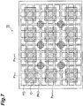
- FIG. 7 is a diagram illustrating respective layout regions of the photodiode PD and the capacitance portion C 1 in the photodetecting unit 10.
- FIG. 7 is a view when viewed in a direction perpendicular to the first principal surface of the semiconductor substrate 100. Further, in FIG. 7 , the number of photodiodes PD in each pixel P m,n is assumed to be 9.
- the layout region of the photodiode PD and the layout region of the capacitance portion C 1 of the MIM structure at least partially overlap. It is preferable for an electrode pad layout region PAD to not overlap the layout region of the capacitance portion C 1 and it is preferable to be provided in a region surrounded by pixels of 2 rows and 2 columns or in the vicinity thereof. In the electrode pad layout region PAD, the electrode pads 131 to 133 and other electrode pads are provided, and further, dummy pads may be provided.
- FIG. 8 is a diagram illustrating charge movement in each pixel P m,n of the photodetecting unit 10.
- (a) in FIG. 8 illustrates a state of charge movement when each pixel P m,n includes one photodiode.
- (b) in FIG. 8 illustrates a state of charge movement when each pixel P m,n includes a plurality (12 in (b) in FIG. 8 ) of photodiodes.
- a charge readout time from a junction capacitance portion of the photodiode PD is long because a movement distance of the charge in the photodiode PD is long in a comparative example in which each pixel P m,n includes one photodiode PD.
- each pixel P m,n includes a plurality of photodiodes PD
- the charge readout time from the junction capacitance portion of each photodiode PD to the capacitance portion C 1 is shortened. Therefore, in the solid-state imaging device 1 of the present embodiment, even when the light detection region of each pixel P m,n has a large area, it is possible to shorten the charge readout time from the junction capacitance portion of each photodiode PD.
- Such a solid-state imaging device 1 is suitable for medical use.
- the solid-state imaging device 1 of the present embodiment because a buried photodiode is provided as the photodiode PD of each pixel P m,n , unread charges do not remain when the charge is transferred from the junction capacitance portion of the photodiode PD to the capacitance portion C 1 , and the S/N ratio and linearity in light detection are excellent. Because the capacitance portion C 1 of each pixel P m,n is provided with the MIM structure on the semiconductor substrate 100, it is possible to output a large amount of charge from the capacitance portion C 1 to the signal readout unit 20 without saturation.
- the layout region of the photodiode PD and the layout region of the capacitance portion C 1 at least partially overlap each other in each pixel P m,n , the light detection region of each photodiode PD can have a large area, and the capacitance portion C 1 can have a large area and a large capacitance.
- the solid-state imaging device 1 of the present embodiment when the first conductor layer 121 and the second conductor layer 122 of the capacitance portion C 1 are opaque or when the scintillator layer is provided on the second principal surface side of the semiconductor substrate 100, as illustrated in FIG. 6 , it is possible to detect light incident from the second principal surface side of the semiconductor substrate 100 (backside incidence). Further, in light subjected to backside incidence, light which is not absorbed by the photodiode PD and reaches the first conductor layer 121 or the second conductor layer 122 of the capacitance portion C 1 is reflected by the capacitance portion C 1 and is incident on the photodiode PD again so that efficiency of photoelectric conversion is improved.
- the first conductor layer 121 and the second conductor layer 122 of the capacitance portion C 1 and the other layers are transparent, light may be incident from either the first principal surface side or the second principal surface side of the semiconductor substrate 100.
- the solid-state imaging device 1 of the present embodiment it is easy to arrange (tile) a plurality of semiconductor substrates each having the photodetecting unit 10 formed thereon in parallel, and it is possible to easily arrange a plurality of pixels at a constant pitch over the entire photodetecting unit 10 when tiling is performed. Even if each semiconductor substrate on which the photodetecting unit 10 is formed does not have a large area and a large number of pixels, it is possible to realize the photodetecting unit 10 with a large area and a large number of pixels as a whole by tiling. Further, because each semiconductor substrate on which the photodetecting unit 10 is formed can have a small area, improvement in manufacturing yield can be expected.
- a solid-state imaging device 2 of the second embodiment is similar to the solid-state imaging device 1 of the first embodiment in terms of the entire configuration illustrated in FIG. 1 , the examples of the cross-sectional structures illustrated in FIG. 5 and FIG. 6 , and the layout regions of the photodiode PD and the capacitance portion C 1 illustrated in FIG. 7 .
- the solid-state imaging device 2 of the second embodiment is different from the solid-state imaging device 1 of the first embodiment in terms of the circuit configuration of each pixel P m,n .
- FIG. 9 is a circuit diagram of a pixel P m,n and an integration circuit 21 n of the solid-state imaging device 2 of the second embodiment.
- FIG. 9 illustrates two pixels P m,n and P m+1,n of an n-th column as representatives of M ⁇ N pixels P 1,1 to P M,N , and illustrates an n-th integration circuit 21 n as a representative of N integration circuits 21 1 to 21 N .
- the pixel P m,n in the second embodiment illustrated in FIG. 9 is different from the pixel P m,n in the first embodiment illustrated in FIG. 2 in that a second transfer switch SW 3 and an initialization switch SW 4 are further included.
- Each of the second transfer switch SW 3 and the initialization switch SW 4 may also be configured by a MOS transistor.
- the second transfer switch SW 3 is provided between a transfer switch SW 1 and a capacitance portion C 1 .
- the charge can be transferred from a junction capacitance portion of a photodiode PD to the capacitance portion C 1 .
- the initialization switch SW 4 is provided between a reference potential terminal to which a reference potential Vref is applied and the transfer switch SW 1 .
- the initialization switch SW 4 can initialize charge accumulation in the junction capacitance portion of each photodiode PD when the switch is in the ON state.
- An ON/OFF operation of the second transfer switch SW 3 of each pixel P m,n is controlled by a control signal ⁇ tran2 output from a control unit 30.
- An ON/OFF operation of the initialization switch SW 4 of each pixel P m,n is controlled by a control signal ⁇ r output from the control unit 30.
- FIG. 10 is a circuit diagram of the pixel P m,n , the pixel P m+1,n , a pixel P m,n+1 , and a pixel P m+1,n+1 of the solid-state imaging device 2 of the second embodiment.
- FIG. 10 illustrates pixels of 2 rows and 2 columns as representatives of M rows and N columns.
- a control signal ⁇ tran, a control signal ⁇ sel(m), and a charge signal out(n) are similar to those in the first embodiment.
- the control unit 30 applies the common control signal ⁇ tran2 to the M ⁇ N pixels P 1,1 to P M,N .
- the control signal ⁇ tran2 is a signal for controlling the ON/OFF operations of the second transfer switches SW 3 of all of the pixels.
- the control unit 30 applies the common control signal ⁇ r to the M ⁇ N pixels P 1,1 to P M,N .
- the control signal ⁇ r is a signal for controlling the ON/OFF operations of the initialization switches SW 4 of all of the pixels.
- FIG. 11 is a timing chart illustrating an example of an operation of the solid-state imaging device 2 of the second embodiment.
- FIG. 11 illustrates the control signal ⁇ tran to be applied to the transfer switch SW 1 of each pixel P m,n , the control signal ⁇ r to be applied to the initialization switch SW 4 of each pixel P m,n , the control signal ⁇ tran2 to be applied to the second transfer switch SW 3 of each pixel P m,n , the control signal ⁇ reset to be applied to the initialization switch SW 21 of each integration circuit 21 n , and the control signals ⁇ sel(1) to ⁇ sel(M) to be applied to the output switch SW 2 of the pixel P m,n of each row.
- Each switch is assumed to be in the ON state when the applied control signal has a high level.
- the control signal ⁇ tran has the high level in a constant cycle, and the transfer switches SW 1 of all of the pixels alternately repeat the ON state period and the OFF state period in a constant cycle.
- the transfer switches SW 1 are in the OFF state in all of the pixels, and the charge generated according to the light incidence on each photodiode PD is accumulated in the junction capacitance portion of the photodiode PD.
- the transfer switches SW 1 are in the ON state in all of the pixels.
- the control signals ⁇ sel(1) to ⁇ sel(M) have the low level, and the output switches SW 2 are in the OFF state in all of the pixels.
- the control signal ⁇ tran2 has the high level, and the second transfer switches SW 3 are in the ON state in all of the pixels.
- the control signal ⁇ r has the low level, and the initialization switches SW 4 are in the OFF state in all of the pixels.
- the control signal ⁇ tran2 has the low level, and the second transfer switches SW 3 are in the OFF state in all of the pixels. Further, the control signal ⁇ r has the high level, and the initialization switches SW 4 are in the ON state in all of the pixels.
- the reference potential Vref is applied to each photodiode via the initialization switch SW 4 and the transfer switch SW 1 , and the charge accumulation in the junction capacitance portion of each photodiode is initialized.
- the control signal ⁇ reset has the high level in a period in which the control signal ⁇ tran2 has the high level, and the control signal ⁇ reset also has the high level at a constant interval in the subsequent period (charge accumulation period) in which the control signal ⁇ tran2 has the low level.
- the initialization switch SW 21 is in the ON state in each of the N integration circuits 21 1 to 21 N , and the charge accumulation in the capacitance portion C 21 is initialized.
- any one control signal ⁇ sel(m) of the control signals ⁇ sel(1) to ⁇ sel(M) has the high level in the period in which the control signal ⁇ reset has the low level.
- the output switch SW 2 is in the ON state in each of the N pixels P m,1 to P m,N of the m-th row to which the control signal ⁇ sel(m) having the high level is applied, and the charge accumulated in the capacitance portion C 1 is output as the charge signal out(n).
- the charge signal out(n) is input to the n-th integration circuit 21 n and accumulated in the capacitance portion C 21 , and a voltage value according to the amount of accumulated charge is output from the integration circuit 21 n .
- the control unit 30 initializes the charge accumulation in the junction capacitance portion of each photodiode PD by setting the initialization switches SW 4 and the transfer switches SW 1 in all of the pixels to the ON state. After the initialization, the control unit 30 causes the charge generated according to the light incidence to be accumulated in the junction capacitance portion of each photodiode PD in all of the pixels during the common charge accumulation period. After the charge accumulation period, the control unit 30 causes the charge to be transferred from the junction capacitance portion of each photodiode PD to the capacitance portion C 1 by setting the transfer switches SW 1 and the second transfer switches SW 3 in all of the pixels to the ON state.
- control unit 30 causes the charge to be output from the capacitance portion C 1 to the signal readout unit 20 by sequentially setting the output switches SW 2 to the ON state for respective rows.
- the control unit 30 can cause the charge to be output from the capacitance portion C 1 of each pixel to the signal readout unit 20 in the charge accumulation period in which the charge is accumulated in the junction capacitance portion of each photodiode PD.
- the second embodiment also, advantageous effects similar to those of the first embodiment can be obtained.
- a solid-state imaging device 3 of the third embodiment is similar to the solid-state imaging device 1 of the first embodiment in terms of the entire configuration illustrated in FIG. 1 , the examples of the cross-sectional structures illustrated in FIG. 5 and FIG. 6 , and the layout regions of the photodiode PD and the capacitance portion C 1 illustrated in FIG. 7 .
- the solid-state imaging device 3 of the third embodiment is different from the solid-state imaging device 1 of the first embodiment in terms of the circuit configuration of each pixel P m,n .
- FIG. 12 is a circuit diagram of a pixel P m,n and an integration circuit 21 n of the solid-state imaging device 3 of the third embodiment.
- FIG. 12 illustrates two pixels P m,n and P m+1,n of an n-th column as representatives of M ⁇ N pixels P 1,1 to P M,N , and illustrates an n-th integration circuit 21 n as a representative of N integration circuits 21 1 to 21 N .
- the pixel P m,n in the third embodiment illustrated in FIG. 12 is different from the pixel P m,n in the first embodiment illustrated in FIG. 2 in that an initialization switch SW 4 is further included.
- the initialization switch SW 4 may also be configured by a MOS transistor.
- the initialization switch SW 4 is provided between a reference potential terminal to which a reference potential Vref is applied and a photodiode PD.
- the initialization switch SW 4 can initialize charge accumulation in a junction capacitance portion of each photodiode PD when the switch is in an ON state.
- An ON/OFF operation of the initialization switch SW 4 of each pixel P m,n is controlled by a control signal ⁇ r output from a control unit 30.
- FIG. 13 is a circuit diagram of the pixel P m,n , the pixel P m+1,n , a pixel P m,n+1 , and a pixel P m+1,n+1 of the solid-state imaging device 3 of the third embodiment.
- FIG. 13 illustrates pixels of 2 rows and 2 columns as representatives of M rows and N columns.
- a control signal ⁇ tran, a control signal ⁇ sel(m), and a charge signal out(n) are similar to those in the first embodiment.
- the control unit 30 applies the common control signal ⁇ r to the M ⁇ N pixels P 1,1 to P M,N .
- the control signal ⁇ r is a signal for controlling ON/OFF operations of the initialization switches SW 4 of all of the pixels.
- FIG. 14 is a timing chart illustrating an example of an operation of the solid-state imaging device 3 of the third embodiment.
- FIG. 14 illustrates the control signal ⁇ r to be applied to the initialization switch SW 4 of each pixel P m,n , the control signal ⁇ tran to be applied to the transfer switch SW 1 of each pixel P m,n , the control signal ⁇ reset to be applied to the initialization switch SW 21 of each integration circuit 21 n , and the control signals ⁇ sel(1) to ⁇ sel(M) to be applied to the output switch SW 2 of the pixel P m,n of each row.
- Each switch is assumed to be in the ON state when the applied control signal has a high level.
- the control signal ⁇ r has the high level and the initialization switches SW 4 are in the ON state in all of the pixels.
- the reference potential Vref is applied to each photodiode via the initialization switch SW 4 and the charge accumulation in the junction capacitance portion of each photodiode is initialized.
- each transfer switch SW 1 and each initialization switch SW 4 are in an OFF state, and the charge generated according to the light incidence on each photodiode PD is accumulated in the junction capacitance portion of the photodiode PD.
- the transfer switches SW 1 are in the ON state in all of the pixels, and further, the control signals ⁇ sel(1) to ⁇ sel(M) have the low level, and the output switches SW 2 are in the OFF state in all of the pixels.
- the charge accumulated until then in the junction capacitance portion of each photodiode PD is transferred to the capacitance portion C 1 via the transfer switch SW 1 .
- the control signal ⁇ reset has the high level in a period in which the control signal ⁇ tran has the high level, and the control signal ⁇ reset also has the high level at a constant interval in a subsequent period in which the control signal ⁇ tran has the low level.
- the initialization switch SW 21 is in the ON state in each of the N integration circuits 21 1 to 21 N , and the charge accumulation in the capacitance portion C 21 is initialized.
- any one control signal ⁇ sel(m) of the control signals ⁇ sel(1) to ⁇ sel(M) has the high level in the period in which the control signal ⁇ reset has the low level.
- the output switch SW 2 is in the ON state in each of the N pixels P m,1 to P m,N of the m-th row to which the control signal ⁇ sel(m) having the high level is applied, and the charge accumulated in the capacitance portion C 1 is output as the charge signal out(n).
- the charge signal out(n) is input to the n-th integration circuit 21 n and accumulated in the capacitance portion C 21 , and a voltage value according to the amount of accumulated charge is output from the integration circuit 21 n .
- the control unit 30 initializes the charge accumulation in the junction capacitance portion of each photodiode PD by setting the initialization switches SW 4 in all of the pixels to the ON state. After the initialization, the control unit 30 causes the charge generated according to the light incidence to be accumulated in the junction capacitance portion of each photodiode PD in all of the pixels during the common charge accumulation period. After the charge accumulation period, the control unit 30 causes the charge to be transferred from the junction capacitance portion of each photodiode PD to the capacitance portion C 1 by setting the transfer switches SW 1 in all of the pixels to the ON state.
- control unit 30 causes the charge to be output from the capacitance portion C 1 to the signal readout unit 20 by sequentially setting the output switches SW 2 to the ON state for respective rows.
- the control unit 30 can cause the charge to be output from the capacitance portion C 1 of each pixel to the signal readout unit 20 in the charge accumulation period in which the charge is accumulated in the junction capacitance portion of each photodiode PD.
- advantageous effects similar to those of the second embodiment can be obtained.
- a solid-state imaging device 4 of the fourth embodiment is different from those of the above-described first to third embodiments in that a signal readout unit 20 is provided on a support substrate 50.
- FIG. 15 is a diagram illustrating an example of a cross-sectional structure of the solid-state imaging device 4 of the fourth embodiment.
- the signal readout unit 20 and a control unit 30 are provided on the support substrate 50.
- the signal readout unit 20 and the control unit 30 may be provided on the support substrate 50 in a state of a chip or may be provided on the support substrate 50 in a state in which the units are placed in a package.
- wiring between the photodetecting unit 10, the signal readout unit 20, and the control unit 30 can be shortened, there is an effect of noise reduction.
- a solid-state imaging device 5 of the fifth embodiment is different from those of the above-described first to third embodiments in that a signal readout unit 20 is provided on a first principal surface of a semiconductor substrate 100.
- FIG. 16 is a diagram illustrating an example of a cross-sectional structure of the solid-state imaging device 5 of the fifth embodiment.
- the signal readout unit 20 and a control unit 30 are provided on the first principal surface of the semiconductor substrate 100.
- the signal readout unit 20 and the control unit 30 are connected to a photodetecting unit 10 via a bump.
- wiring between the photodetecting unit 10, the signal readout unit 20, and the control unit 30 can be shortened, there is an effect of noise reduction.
- a solid-state imaging device 6 of the sixth embodiment is different from those of the above-described first to third embodiments in that a light detection region of a photodiode PD of each pixel is selectively thinned in a second principal surface side of a semiconductor substrate 100.
- FIG. 17 is a diagram illustrating an example of a cross-sectional structure of the solid-state imaging device 6 of the sixth embodiment.
- the photodiode PD of each pixel is selectively thinned on the second principal surface (a lower surface in FIG. 17 ) side of the semiconductor substrate 100, and therefore loss when light incident from the second principal surface side passes through the semiconductor substrate 100 is reduced, the photodiode PD can detect light with high sensitivity.
- the solid-state imaging device according to the present invention is not limited to the above-described embodiments and configuration examples, and various modifications are possible.
- the solid-state imaging device is configured to include a photodetecting unit including a plurality of pixels on a first principal surface of a semiconductor substrate having the first principal surface and a second principal surface opposite to each other; a signal readout unit outputting a signal value according to an amount of charge output from each of the plurality of pixels; and a control unit controlling an operation of each of the photodetecting unit and the signal readout unit.
- each of the plurality of pixels includes a plurality of buried photodiodes each of which generates a charge according to light incidence and accumulates the charge in a junction capacitance portion; a capacitance portion accumulating the charge transferred from the junction capacitance portion of each of the plurality of photodiodes; a transfer switch group for transferring the charge from the junction capacitance portion of each of the plurality of photodiodes to the capacitance portion; and an output switch for outputting the charge from the capacitance portion to the signal readout unit.
- control unit performs control so as to accumulate the charge generated according to the light incidence in each of the plurality of pixels in the junction capacitance portion of each photodiode during a common charge accumulation period, transfer the charge from the junction capacitance portion of each photodiode to the capacitance portion by setting the transfer switch group to an ON state in each of the plurality of pixels after the charge accumulation period, and output the charge from the capacitance portion to the signal readout unit by sequentially setting the output switch to an ON state in each of the plurality of pixels after charge transfer.
- the capacitance portion may be provided on the first principal surface of the semiconductor substrate and may be configured such that an insulator layer is sandwiched between a first conductor layer and a second conductor layer.
- a layout region of the photodiode and a layout region of the capacitance portion may be configured to at least partially overlap each other in each of the plurality of pixels when viewed in a direction perpendicular to the first principal surface.
- each of the plurality of pixels may further include an initialization switch group for initializing charge accumulation in the junction capacitance portion of each of the plurality of photodiodes
- the control unit may control so as to initialize the charge accumulation in the junction capacitance portion of each photodiode by setting the initialization switch group to an ON state in each of the plurality of pixels before the charge accumulation period.
- the above-described solid-state imaging device may further include a scintillator layer provided on the second principal surface side of the semiconductor substrate.
- the above-described solid-state imaging device may further include a support substrate provided on the first principal surface side of the semiconductor substrate and supporting the semiconductor substrate. Further, in this case, the signal readout unit may be provided on the support substrate.
- the signal readout unit may be provided on the first principal surface of the semiconductor substrate.
- a light detection region of the photodiode of each of the plurality of pixels may be selectively thinned in the second principal surface side of the semiconductor substrate.
- the present invention can be used as a solid-state imaging device which can shorten a charge readout time from a junction capacitance portion of a photodiode of each pixel and which has an excellent S/N ratio and linearity in light detection.
Landscapes
- Engineering & Computer Science (AREA)
- Signal Processing (AREA)
- Multimedia (AREA)
- Physics & Mathematics (AREA)
- General Physics & Mathematics (AREA)
- Molecular Biology (AREA)
- Spectroscopy & Molecular Physics (AREA)
- High Energy & Nuclear Physics (AREA)
- Life Sciences & Earth Sciences (AREA)
- Health & Medical Sciences (AREA)
- Transforming Light Signals Into Electric Signals (AREA)
- Solid State Image Pick-Up Elements (AREA)
- Measurement Of Radiation (AREA)
- Electromagnetism (AREA)
Abstract
Description
- The present invention relates to a solid-state imaging device.
- A solid-state imaging device includes a photodetecting unit having a plurality of pixels on a principal surface of a semiconductor substrate, and a signal readout unit that reads out a charge from each of the plurality of pixels and outputs a signal value according to an amount of charge (see
Patent Documents 1 to 5). Each of the plurality of pixels includes a photodiode that generates a charge according to light incidence. The signal readout unit includes an integration circuit in which an integration capacitance portion is provided between an input terminal and an output terminal of an amplifier, accumulates a charge generated in the photodiode of each pixel in the integration capacitance portion, and outputs a signal value according to an amount of accumulated charge. -
- Patent Document 1: Japanese Patent Application Laid-Open Publication No.
2000-32342 - Patent Document 2: Japanese Patent Application Laid-Open Publication No.
H9-247536 - Patent Document 3: Japanese Patent Publication No.
2719058 - Patent Document 4: Japanese Patent Publication No.
4878123 - Patent Document 5: Japanese Patent Publication No.
3825503 - A solid-state imaging device described in
Patent Document 1 includes an integration circuit common to a plurality of pixels. A solid-state imaging device having such a configuration accumulates a charge generated in a photodiode according to light incidence in each of a plurality of pixels in a junction capacitance portion of the photodiode, sequentially transfers the charge accumulated in the junction capacitance portion of the photodiode of each pixel to an integration capacitance portion of the common integration circuit, and outputs a signal value according to an amount of charge from the integration circuit. - When unread charges remain in the junction capacitance portion when the charge is transferred from the junction capacitance portion of the photodiode of each pixel to the integration capacitance portion of the integration circuit, an S/N ratio and linearity of light detection deteriorate. To solve such a problem, a buried photodiode may be used as the photodiode of each pixel. When the buried photodiode is used with full depletion, junction capacitance decreases, an output voltage changes linearly with respect to an amount of accumulated charge, and a charge generated in a pn junction portion can be almost completely read out such that the S/N ratio and linearity in light detection are excellent.
- However, the buried photodiode has higher resistance than a normal photodiode. Further, an area of a light detection region of a photodiode of a solid-state imaging device in medical applications (for example, for X-ray detection in X-ray CT) is about 100 times that of a usual application (for example, for capturing an optical image in a digital camera). When such a buried photodiode having a large area and high resistance is used, a charge readout time from the junction capacitance portion of the photodiode is lengthened.
- The present invention has been made in order to solve the above problem, and an object thereof is to provide a solid-state imaging device which can shorten a charge readout time from a junction capacitance portion of a photodiode of each pixel and which has an excellent S/N ratio and linearity in light detection.
- A solid-state imaging device according to the present invention includes a photodetecting unit including a plurality of pixels on a first principal surface of a semiconductor substrate having the first principal surface and a second principal surface opposite to each other; a signal readout unit outputting a signal value according to an amount of charge output from each of the plurality of pixels; and a control unit controlling an operation of each of the photodetecting unit and the signal readout unit. Further, each of the plurality of pixels includes a plurality of buried photodiodes each of which generates a charge according to light incidence and accumulates the charge in a junction capacitance portion; a capacitance portion accumulating the charge transferred from the junction capacitance portion of each of the plurality of photodiodes; a transfer switch group for transferring the charge from the junction capacitance portion of each of the plurality of photodiodes to the capacitance portion; and an output switch for outputting the charge from the capacitance portion to the signal readout unit. Further, the control unit controls so as to accumulate the charge generated according to the light incidence in each of the plurality of pixels in the junction capacitance portion of each photodiode during a common charge accumulation period, transfer the charge from the junction capacitance portion of each photodiode to the capacitance portion by setting the transfer switch group to an ON state in each of the plurality of pixels after the charge accumulation period, and output the charge from the capacitance portion to the signal readout unit by sequentially setting the output switch to an ON state in each of the plurality of pixels after charge transfer.
- According to the present invention, it is possible to provide a solid-state imaging device which can shorten a charge readout time from a junction capacitance portion of a photodiode of each pixel and which has an excellent S/N ratio and linearity in light detection.
-
- [
FIG. 1] FIG. 1 is an entire configuration diagram of a solid-state imaging device 1 of a first embodiment. - [
FIG. 2] FIG. 2 is a circuit diagram of a pixel Pm,n and an integration circuit 21n of the solid-state imaging device 1 of the first embodiment. - [
FIG. 3] FIG. 3 is a circuit diagram of the pixel Pm,n, a pixel Pm+1,n, a pixel Pm,n+1, and a pixel Pm+1,n+1 of the solid-state imaging device 1 of the first embodiment. - [
FIG. 4] FIG. 4 is a timing chart illustrating an example of an operation of the solid-state imaging device 1 of the first embodiment. - [
FIG. 5] FIG. 5 is a diagram illustrating an example of a cross-sectional structure of a photodetectingunit 10 of the solid-state imaging device 1 of the first embodiment. - [
FIG. 6] FIG. 6 is a diagram illustrating an example of a cross-sectional structure of the solid-state imaging device 1 of the first embodiment. - [
FIG. 7] FIG. 7 is a view illustrating respective layout regions of a photodiode PD and a capacitance portion C1 in the photodetectingunit 10. - [
FIG. 8] FIG. 8 is a diagram illustrating charge movement in each pixel Pm,n of the photodetectingunit 10, and illustrates (a) a state of charge movement when each pixel Pm,n includes one photodiode and (b) a state of charge movement when each pixel Pm,n includes a plurality of photodiodes. - [
FIG. 9] FIG. 9 is a circuit diagram of a pixel Pm,n and an integration circuit 21n of a solid-state imaging device 2 of a second embodiment. - [
FIG. 10] FIG. 10 is a circuit diagram of the pixel Pm,n, a pixel Pm+1,n, a pixel Pm,n+1, and a pixel Pm+1,n+1 of the solid-state imaging device 2 of the second embodiment. - [
FIG. 11] FIG. 11 is a timing chart illustrating an example of an operation of the solid-state imaging device 2 of the second embodiment. - [
FIG. 12] FIG. 12 is a circuit diagram of a pixel Pm,n and an integration circuit 21n of a solid-state imaging device 3 of a third embodiment. - [
FIG. 13] FIG. 13 is a circuit diagram of the pixel Pm,n, a pixel Pm+1,n, a pixel Pm,n+1, and a pixel Pm+1,n+1 of the solid-state imaging device 3 of the third embodiment and illustrates pixels of two rows and two columns as representatives of M rows and N columns. - [
FIG. 14] FIG. 14 is a timing chart illustrating an example of an operation of the solid-state imaging device 3 of the third embodiment. - [
FIG. 15] FIG. 15 is a diagram illustrating an example of a cross-sectional structure of a solid-state imaging device 4 of a fourth embodiment. - [
FIG. 16] FIG. 16 is a diagram illustrating an example of a cross-sectional structure of a solid-state imaging device 5 of a fifth embodiment. - [
FIG. 17] FIG. 17 is a diagram illustrating an example of a cross-sectional structure of a solid-state imaging device 6 of a sixth embodiment. - Hereinafter, embodiments for carrying out the present invention will be described in detail with reference to the accompanying drawings. In the description of the drawings, the same or equivalent elements will be denoted by the same reference signs, without redundant description.
-
FIG. 1 is an entire configuration diagram of a solid-state imaging device 1 of the first embodiment. The solid-state imaging device 1 includes a photodetectingunit 10 and asignal readout unit 20, and further includes acontrol unit 30 that controls respective operations of the photodetectingunit 10 and thesignal readout unit 20. - The photodetecting
unit 10 has M×N pixels P1,1 to PM,N on a first principal surface of a semiconductor substrate having the first principal surface and a second principal surface opposite to each other. The M×N pixels P1,1 to PM,N have a common configuration and are arrayed two-dimensionally. A pixel Pm,n is located in an m-th row and an n-th column. Each pixel Pm,n includes a photodiode that generates a charge according to light incidence and can output the charge. Here, M and N are each an integer of 2 or more. m is an integer of 1 or more and M or less. n is an integer of 1 or more and N or less. - The
signal readout unit 20 outputs a signal value according to an amount of charge output from each of the M×N pixels P1,1 to PM,N. Thesignal readout unit 20 includes N integration circuits 211 to 21N, N hold circuits 221 to 22N, and anAD conversion circuit 23. The N integration circuits 211 to 21N have a common configuration. The N hold circuits 221 to 22N have a common configuration. - The n-th integration circuit 21n inputs the charge sequentially output from each of the M pixels P1,n to PM,n of the n-th column, and outputs a voltage value according to the amount of charge to the hold circuit 22n. The n-th hold circuit 22n inputs and holds the voltage value output from the integration circuit 21n. The N hold circuits 221 to 22N sequentially output voltage values held thereby to the
AD conversion circuit 23. - The
AD conversion circuit 23 inputs a voltage value sequentially output from each of the N hold circuits 221 to 22N, converts the input voltage value into a digital value, and outputs the digital value. The digital value output from theAD conversion circuit 23 is a signal value according to an amount of charge output from each of the M×N pixels P1,1 to PM,N. -
FIG. 2 is a circuit diagram of the pixel Pm,n and the integration circuit 21n of the solid-state imaging device 1 of the first embodiment.FIG. 2 illustrates two pixels Pm,n and Pm+1,n of the n-th column as representatives of the M×N pixels P1,1 to PM,N, and illustrates the n-th integration circuit 21n as a representative of the N integration circuits 211 to 21N. - Each pixel Pm,n includes a plurality of buried photodiodes PD, a capacitance portion C1, a plurality of transfer switches SW1, and an output switch SW2. Each of the transfer switches SW1 and the output switch SW2 may be configured by a MOS transistor. Each photodiode PD can generate a charge according to the light incidence and accumulate the charge in a junction capacitance portion. The capacitance portion C1 accumulates the charge transferred from the junction capacitance portion of each of the plurality of photodiodes PD via the transfer switch SW1. In each pixel Pm,n, one capacitance portion C1 may be provided or a plurality of partial capacitance portions may be provided in parallel.
- Each transfer switch SW1 is provided in a one-to-one correspondence with the photodiode PD. Each pair of the photodiode PD and the transfer switch SW1 is provided in parallel to the capacitance portion C1. Each transfer switch SW1 can transfer the charge from the junction capacitance portion of the photodiode PD to the capacitance portion C1 in an ON state. The output switch SW2 can output the charge from the capacitance portion C1 to the integration circuit 21n of the
signal readout unit 20 in an ON state. - Each integration circuit 21n includes an amplifier A21, a capacitance portion C21, and an initialization switch SW21. The capacitance portion C21 and the initialization switch SW21 are connected in parallel and are provided between an input terminal and an output terminal of the amplifier A21. The initialization switch SW21 may be configured by a MOS transistor. When the initialization switch SW21 is in an ON state, charge accumulation in the capacitance portion C21 is initialized. When the initialization switch SW21 is in an OFF state, the capacitance portion C21 can accumulate the input charge. The integration circuit 21n outputs a voltage value according to the amount of accumulated charge in the capacitance portion C21.
- An ON/OFF operation of the transfer switch SW1 of each pixel Pm,n is controlled by a control signal φtran output from the
control unit 30. An ON/OFF operation of the output switch SW2 of each pixel Pm,n is controlled by a control signal φsel(m) output from thecontrol unit 30. An ON/OFF operation of the initialization switch SW21 of each integration circuit 21n is controlled by a control signal φreset output from thecontrol unit 30. -
FIG. 3 is a circuit diagram of the pixel Pm,n, the pixel Pm+1,n, a pixel Pm,n+1, and a pixel Pm+1,n+1 of the solid-state imaging device 1 of the first embodiment.FIG. 3 illustrates pixels of two rows and two columns as representatives of M rows and N columns. - The
control unit 30 applies the common control signal φtran to the M×N pixels P1,1 to PM,N. The control signal φtran is a signal for controlling the ON/OFF operations of the transfer switches SW1 of all of the pixels. Thecontrol unit 30 applies the common control signal φsel(m) to the N pixels Pm,1 to Pm,N of the m-th row. The control signal φsel(m) is a signal for controlling the ON/OFF operations of the output switches SW2 of the N pixels of the m-th row. A period in which the output switch SW2 is in the ON state according to the control signal is different in the first to M-th rows. The n-th integration circuit 21n inputs a charge signal out(n) sequentially output from the output switch SW2 of each of the M pixels P1,n to PM,n of the n-th column. -
FIG. 4 is a timing chart illustrating an example of an operation of the solid-state imaging device 1 of the first embodiment.FIG. 4 illustrates the control signal φtran to be applied to the transfer switch SW1 of each pixel Pm,n, the control signal φreset to be applied to the initialization switch SW21 of each integration circuit 21n, and the control signals φsel(1) to φsel(M) to be applied to the output switch SW2 of the pixel Pm,n of each row. Each switch is assumed to be in the ON state when the applied control signal has a high level. - The control signal φtran has the high level in a constant cycle, and the transfer switches SW1 of all of the pixels alternately repeat the ON state period and the OFF state period in a constant cycle.
- During a period (charge accumulation period) in which the control signal φtran has a low level, the transfer switches SW1 are in the OFF state in all of the pixels, and the charge generated according to the light incidence on each photodiode PD is accumulated in the junction capacitance portion of the photodiode PD.
- During a period in which the control signal φtran has the high level, the transfer switches SW1 are in the ON state in all of the pixels, and further, the control signals φsel(1) to φsel(M) have the low level, and the output switches SW2 are in the OFF state in all of the pixels. Thereby, in all of the pixels, the charge accumulated until then in the junction capacitance portion of each photodiode PD is transferred to the capacitance portion C1 via the transfer switch SW1.
- The control signal φreset has the high level in the period in which the control signal φtran has the high level, and the control signal φreset also has the high level at a constant interval in a subsequent period (charge accumulation period) in which the control signal φtran has the low level. When the control signal φreset has the high level, the initialization switch SW21 is in the ON state in each of the N integration circuits 211 to 21N, and the charge accumulation in the capacitance portion C21 is initialized.
- Any one control signal φsel(m) of the control signals φsel(1) to φsel(M) has the high level in the period in which the control signal φreset has the low level. Thereby, the output switch SW2 is in the ON state in each of the N pixels Pm,1 to Pm,N of the m-th row to which the control signal φsel(m) having the high level is applied, and the charge accumulated in the capacitance portion C1 is output as the charge signal out(n). The charge signal out(n) is input to the n-th integration circuit 21n and accumulated in the capacitance portion C21, and a voltage value according to the amount of accumulated charge is output from the integration circuit 21n.
- That is, the
control unit 30 causes the charge generated according to the light incidence to be accumulated in the junction capacitance portion of each photodiode PD in all of the pixels during the common charge accumulation period. After the charge accumulation period, thecontrol unit 30 causes the charge to be transferred from the junction capacitance portion of each photodiode PD to the capacitance portion C1 by setting the transfer switches SW1 to the ON state in all of the pixels. Then, after the charge is transferred, thecontrol unit 30 causes the charge to be output from the capacitance portion C1 to thesignal readout unit 20 by sequentially setting the output switches SW2 to the ON state for respective rows. Thecontrol unit 30 can cause the charge to be output from the capacitance portion C1 of each pixel to thesignal readout unit 20 in the charge accumulation period in which the charge is accumulated in the junction capacitance portion of each photodiode PD. -
FIG. 5 is a diagram illustrating an example of a cross-sectional structure of thephotodetecting unit 10 of the solid-state imaging device 1 of the first embodiment.FIG. 5 schematically illustrates an example of a cross-sectional structure of the two pixels Pm,n and Pm+1,n of the n-th column as representatives of the M×N pixels P1,1 to PM,N. Further, inFIG. 5 , the number of photodiodes PD of each pixel Pm,n is assumed to be 2. - The
photodetecting unit 10 includes a p-typefirst semiconductor region 101, an n--typesecond semiconductor region 102, a p+-typethird semiconductor region 103, an n+-typefourth semiconductor region 104, an n+-typefifth semiconductor region 105, aninsulator layer 107,gate electrodes first conductor layer 121, asecond conductor layer 122, aninsulator layer 123, andelectrode pads 131 to 133, formed on the first principal surface (an upper surface inFIG. 5 ) of thesemiconductor substrate 100. - The p-type
first semiconductor region 101 is widely formed on the first principal surface of thesemiconductor substrate 100. The n--typesecond semiconductor region 102 is formed on a partial range of the p-typefirst semiconductor region 101. The p+-typethird semiconductor region 103 is formed on both the p-typefirst semiconductor region 101 and the n--typesecond semiconductor region 102. Each of the n+-typefourth semiconductor region 104 and the n+-typefifth semiconductor region 105 is formed on the p-typefirst semiconductor region 101. Theinsulator layer 107 is formed on substantially the entire semiconductor regions except a part thereof. - The
gate electrode 111 is provided above the p-typefirst semiconductor region 101 between the n--typesecond semiconductor region 102 and the n+-typefourth semiconductor region 104, and is formed on theinsulator layer 107. Thegate electrode 112 is provided above the p-typefirst semiconductor region 101 between the n+-typefourth semiconductor region 104 and the n+-typefifth semiconductor region 105, and is formed on theinsulator layer 107. Thefirst conductor layer 121, thesecond conductor layer 122, and theinsulator layer 123 are provided above the semiconductor regions and formed on theinsulator layer 107. - The p-type
first semiconductor region 101, the n--typesecond semiconductor region 102, and the p+-typethird semiconductor region 103 constitute the buried photodiode PD. The buried photodiode PD has an excellent S/N ratio and linearity in light detection. - The
first conductor layer 121 and thesecond conductor layer 122 sandwiching theinsulator layer 123 constitute the capacitance portion C1 of an MIM (metal insulator metal) structure. For example, each of thefirst conductor layer 121 and thesecond conductor layer 122 is a metal layer or a polysilicon layer, and theinsulator layer 123 is an oxide film such as SiO2. - The p-type
first semiconductor region 101, the n--typesecond semiconductor region 102, the n+-typefourth semiconductor region 104, and thegate electrode 111 constitute a MOS transistor, which is the transfer switch SW1. Thegate electrode 111 is electrically connected to theelectrode pad 131, and the control signal φtran is applied thereto via theelectrode pad 131. The n+-typefourth semiconductor region 104 is electrically connected to thesecond conductor layer 122. - The p-type
first semiconductor region 101, the n+-typefourth semiconductor region 104, the n+-typefifth semiconductor region 105, and thegate electrode 112 constitute a MOS transistor, which is the output switch SW2. Thegate electrode 112 is electrically connected to theelectrode pad 132, and the control signal φsel(m) is applied thereto via theelectrode pad 132. The n+-typefifth semiconductor region 105 is electrically connected to theelectrode pad 133, and outputs the charge signal out(n) via theelectrode pad 133. -
FIG. 6 is a diagram illustrating an example of a cross-sectional structure of the solid-state imaging device 1 of the first embodiment.FIG. 6 illustrates a cross-sectional view of thephotodetecting unit 10, ascintillator layer 40, and asupport substrate 50, and illustrates a block diagram of thesignal readout unit 20 and thecontrol unit 30. - The
scintillator layer 40 is provided on the second principal surface (a lower surface inFIG. 6 ) side of thesemiconductor substrate 100, and generates scintillation light according to the incidence of radiation (for example, X-rays or γ-rays). Thesupport substrate 50 is provided on the first principal surface (an upper surface inFIG. 6 ) side of thesemiconductor substrate 100, and supports thesemiconductor substrate 100. Further, thesupport substrate 50, together with acable 60 andbumps 141 to 143, electrically connects thesignal readout unit 20 and thecontrol unit 30 to thephotodetecting unit 10. Thecable 60 is provided between thesignal readout unit 20 and thecontrol unit 30, and thesupport substrate 50. Thebumps 141 to 143 are provided between theelectrode pads 131 to 133 and thesupport substrate 50. -
FIG. 7 is a diagram illustrating respective layout regions of the photodiode PD and the capacitance portion C1 in thephotodetecting unit 10.FIG. 7 is a view when viewed in a direction perpendicular to the first principal surface of thesemiconductor substrate 100. Further, inFIG. 7 , the number of photodiodes PD in each pixel Pm,n is assumed to be 9. - As illustrated in
FIG. 7 , in each pixel Pm,n, the layout region of the photodiode PD and the layout region of the capacitance portion C1 of the MIM structure at least partially overlap. It is preferable for an electrode pad layout region PAD to not overlap the layout region of the capacitance portion C1 and it is preferable to be provided in a region surrounded by pixels of 2 rows and 2 columns or in the vicinity thereof. In the electrode pad layout region PAD, theelectrode pads 131 to 133 and other electrode pads are provided, and further, dummy pads may be provided. -
FIG. 8 is a diagram illustrating charge movement in each pixel Pm,n of thephotodetecting unit 10. (a) inFIG. 8 illustrates a state of charge movement when each pixel Pm,n includes one photodiode. (b) inFIG. 8 illustrates a state of charge movement when each pixel Pm,n includes a plurality (12 in (b) inFIG. 8 ) of photodiodes. - When a pixel having a large area light detection region using a buried photodiode PD which generally has high resistance is configured, as illustrated in (a) in
FIG. 8 , a charge readout time from a junction capacitance portion of the photodiode PD is long because a movement distance of the charge in the photodiode PD is long in a comparative example in which each pixel Pm,n includes one photodiode PD. - On the other hand, as illustrated in (b) in
FIG. 8 , because a movement distance of the charge in each of the photodiodes PD is short in the present embodiment in which each pixel Pm,n includes a plurality of photodiodes PD, the charge readout time from the junction capacitance portion of each photodiode PD to the capacitance portion C1 is shortened. Therefore, in the solid-state imaging device 1 of the present embodiment, even when the light detection region of each pixel Pm,n has a large area, it is possible to shorten the charge readout time from the junction capacitance portion of each photodiode PD. Such a solid-state imaging device 1 is suitable for medical use. - In the solid-
state imaging device 1 of the present embodiment, because a buried photodiode is provided as the photodiode PD of each pixel Pm,n, unread charges do not remain when the charge is transferred from the junction capacitance portion of the photodiode PD to the capacitance portion C1, and the S/N ratio and linearity in light detection are excellent. Because the capacitance portion C1 of each pixel Pm,n is provided with the MIM structure on thesemiconductor substrate 100, it is possible to output a large amount of charge from the capacitance portion C1 to thesignal readout unit 20 without saturation. Because the layout region of the photodiode PD and the layout region of the capacitance portion C1 at least partially overlap each other in each pixel Pm,n, the light detection region of each photodiode PD can have a large area, and the capacitance portion C1 can have a large area and a large capacitance. - In the solid-
state imaging device 1 of the present embodiment, when thefirst conductor layer 121 and thesecond conductor layer 122 of the capacitance portion C1 are opaque or when the scintillator layer is provided on the second principal surface side of thesemiconductor substrate 100, as illustrated inFIG. 6 , it is possible to detect light incident from the second principal surface side of the semiconductor substrate 100 (backside incidence). Further, in light subjected to backside incidence, light which is not absorbed by the photodiode PD and reaches thefirst conductor layer 121 or thesecond conductor layer 122 of the capacitance portion C1 is reflected by the capacitance portion C1 and is incident on the photodiode PD again so that efficiency of photoelectric conversion is improved. Here, when thefirst conductor layer 121 and thesecond conductor layer 122 of the capacitance portion C1 and the other layers are transparent, light may be incident from either the first principal surface side or the second principal surface side of thesemiconductor substrate 100. - Further, in the solid-
state imaging device 1 of the present embodiment, it is easy to arrange (tile) a plurality of semiconductor substrates each having thephotodetecting unit 10 formed thereon in parallel, and it is possible to easily arrange a plurality of pixels at a constant pitch over theentire photodetecting unit 10 when tiling is performed. Even if each semiconductor substrate on which thephotodetecting unit 10 is formed does not have a large area and a large number of pixels, it is possible to realize thephotodetecting unit 10 with a large area and a large number of pixels as a whole by tiling. Further, because each semiconductor substrate on which thephotodetecting unit 10 is formed can have a small area, improvement in manufacturing yield can be expected. - A solid-
state imaging device 2 of the second embodiment is similar to the solid-state imaging device 1 of the first embodiment in terms of the entire configuration illustrated inFIG. 1 , the examples of the cross-sectional structures illustrated inFIG. 5 andFIG. 6 , and the layout regions of the photodiode PD and the capacitance portion C1 illustrated inFIG. 7 . However, the solid-state imaging device 2 of the second embodiment is different from the solid-state imaging device 1 of the first embodiment in terms of the circuit configuration of each pixel Pm,n. -
FIG. 9 is a circuit diagram of a pixel Pm,n and an integration circuit 21n of the solid-state imaging device 2 of the second embodiment.FIG. 9 illustrates two pixels Pm,n and Pm+1,n of an n-th column as representatives of M×N pixels P1,1 to PM,N, and illustrates an n-th integration circuit 21n as a representative of N integration circuits 211 to 21N. - The pixel Pm,n in the second embodiment illustrated in
FIG. 9 is different from the pixel Pm,n in the first embodiment illustrated inFIG. 2 in that a second transfer switch SW3 and an initialization switch SW4 are further included. Each of the second transfer switch SW3 and the initialization switch SW4 may also be configured by a MOS transistor. - The second transfer switch SW3 is provided between a transfer switch SW1 and a capacitance portion C1. When both the transfer switch SW1 and the second transfer switch SW3 are in an ON state, the charge can be transferred from a junction capacitance portion of a photodiode PD to the capacitance portion C1. The initialization switch SW4 is provided between a reference potential terminal to which a reference potential Vref is applied and the transfer switch SW1. The initialization switch SW4 can initialize charge accumulation in the junction capacitance portion of each photodiode PD when the switch is in the ON state.
- An ON/OFF operation of the second transfer switch SW3 of each pixel Pm,n is controlled by a control signal φtran2 output from a
control unit 30. An ON/OFF operation of the initialization switch SW4 of each pixel Pm,n is controlled by a control signal φr output from thecontrol unit 30. -
FIG. 10 is a circuit diagram of the pixel Pm,n, the pixel Pm+1,n, a pixel Pm,n+1, and a pixel Pm+1,n+1 of the solid-state imaging device 2 of the second embodiment.FIG. 10 illustrates pixels of 2 rows and 2 columns as representatives of M rows and N columns. - A control signal φtran, a control signal φsel(m), and a charge signal out(n) are similar to those in the first embodiment. The
control unit 30 applies the common control signal φtran2 to the M×N pixels P1,1 to PM,N. The control signal φtran2 is a signal for controlling the ON/OFF operations of the second transfer switches SW3 of all of the pixels. Thecontrol unit 30 applies the common control signal φr to the M×N pixels P1,1 to PM,N. The control signal φr is a signal for controlling the ON/OFF operations of the initialization switches SW4 of all of the pixels. -
FIG. 11 is a timing chart illustrating an example of an operation of the solid-state imaging device 2 of the second embodiment.FIG. 11 illustrates the control signal φtran to be applied to the transfer switch SW1 of each pixel Pm,n, the control signal φr to be applied to the initialization switch SW4 of each pixel Pm,n, the control signal φtran2 to be applied to the second transfer switch SW3 of each pixel Pm,n, the control signal φreset to be applied to the initialization switch SW21 of each integration circuit 21n, and the control signals φsel(1) to φsel(M) to be applied to the output switch SW2 of the pixel Pm,n of each row. Each switch is assumed to be in the ON state when the applied control signal has a high level. - The control signal φtran has the high level in a constant cycle, and the transfer switches SW1 of all of the pixels alternately repeat the ON state period and the OFF state period in a constant cycle.
- During a period (charge accumulation period) in which the control signal φtran has a low level, the transfer switches SW1 are in the OFF state in all of the pixels, and the charge generated according to the light incidence on each photodiode PD is accumulated in the junction capacitance portion of the photodiode PD.
- During a period in which the control signal φtran has the high level, the transfer switches SW1 are in the ON state in all of the pixels. In a partial period of this period, the control signals φsel(1) to φsel(M) have the low level, and the output switches SW2 are in the OFF state in all of the pixels. The control signal φtran2 has the high level, and the second transfer switches SW3 are in the ON state in all of the pixels. Further, the control signal φr has the low level, and the initialization switches SW4 are in the OFF state in all of the pixels. Thereby, in all of the pixels, the charge accumulated until then in the junction capacitance portion of each photodiode PD is transferred to the capacitance portion C1 via the transfer switch SW1 and the second transfer switch SW3.
- During a period after the above-described certain period (charge transfer period) in the period in which the control signal φtran has the high level, the control signal φtran2 has the low level, and the second transfer switches SW3 are in the OFF state in all of the pixels. Further, the control signal φr has the high level, and the initialization switches SW4 are in the ON state in all of the pixels. Thereby, in all of the pixels, the reference potential Vref is applied to each photodiode via the initialization switch SW4 and the transfer switch SW1, and the charge accumulation in the junction capacitance portion of each photodiode is initialized.
- The control signal φreset has the high level in a period in which the control signal φtran2 has the high level, and the control signal φreset also has the high level at a constant interval in the subsequent period (charge accumulation period) in which the control signal φtran2 has the low level. When the control signal φreset has the high level, the initialization switch SW21 is in the ON state in each of the N integration circuits 211 to 21N, and the charge accumulation in the capacitance portion C21 is initialized.
- Any one control signal φsel(m) of the control signals φsel(1) to φsel(M) has the high level in the period in which the control signal φreset has the low level. Thereby, the output switch SW2 is in the ON state in each of the N pixels Pm,1 to Pm,N of the m-th row to which the control signal φsel(m) having the high level is applied, and the charge accumulated in the capacitance portion C1 is output as the charge signal out(n). The charge signal out(n) is input to the n-th integration circuit 21n and accumulated in the capacitance portion C21, and a voltage value according to the amount of accumulated charge is output from the integration circuit 21n.
- That is, before the charge accumulation period, the
control unit 30 initializes the charge accumulation in the junction capacitance portion of each photodiode PD by setting the initialization switches SW4 and the transfer switches SW1 in all of the pixels to the ON state. After the initialization, thecontrol unit 30 causes the charge generated according to the light incidence to be accumulated in the junction capacitance portion of each photodiode PD in all of the pixels during the common charge accumulation period. After the charge accumulation period, thecontrol unit 30 causes the charge to be transferred from the junction capacitance portion of each photodiode PD to the capacitance portion C1 by setting the transfer switches SW1 and the second transfer switches SW3 in all of the pixels to the ON state. Then, after the charge is transferred, thecontrol unit 30 causes the charge to be output from the capacitance portion C1 to thesignal readout unit 20 by sequentially setting the output switches SW2 to the ON state for respective rows. Thecontrol unit 30 can cause the charge to be output from the capacitance portion C1 of each pixel to thesignal readout unit 20 in the charge accumulation period in which the charge is accumulated in the junction capacitance portion of each photodiode PD. - In the second embodiment also, advantageous effects similar to those of the first embodiment can be obtained. In addition, in the second embodiment, it is possible to reduce an influence of charges remaining in the junction capacitance portion and the parasitic capacitance portion by providing the initialization switch SW4 for initializing the charge accumulation in the junction capacitance portion of the photodiode PD in each pixel.
- A solid-
state imaging device 3 of the third embodiment is similar to the solid-state imaging device 1 of the first embodiment in terms of the entire configuration illustrated inFIG. 1 , the examples of the cross-sectional structures illustrated inFIG. 5 andFIG. 6 , and the layout regions of the photodiode PD and the capacitance portion C1 illustrated inFIG. 7 . However, the solid-state imaging device 3 of the third embodiment is different from the solid-state imaging device 1 of the first embodiment in terms of the circuit configuration of each pixel Pm,n. -
FIG. 12 is a circuit diagram of a pixel Pm,n and an integration circuit 21n of the solid-state imaging device 3 of the third embodiment.FIG. 12 illustrates two pixels Pm,n and Pm+1,n of an n-th column as representatives of M×N pixels P1,1 to PM,N, and illustrates an n-th integration circuit 21n as a representative of N integration circuits 211 to 21N. - The pixel Pm,n in the third embodiment illustrated in
FIG. 12 is different from the pixel Pm,n in the first embodiment illustrated inFIG. 2 in that an initialization switch SW4 is further included. The initialization switch SW4 may also be configured by a MOS transistor. - The initialization switch SW4 is provided between a reference potential terminal to which a reference potential Vref is applied and a photodiode PD. The initialization switch SW4 can initialize charge accumulation in a junction capacitance portion of each photodiode PD when the switch is in an ON state. An ON/OFF operation of the initialization switch SW4 of each pixel Pm,n is controlled by a control signal φr output from a
control unit 30. -
FIG. 13 is a circuit diagram of the pixel Pm,n, the pixel Pm+1,n, a pixel Pm,n+1, and a pixel Pm+1,n+1 of the solid-state imaging device 3 of the third embodiment.FIG. 13 illustrates pixels of 2 rows and 2 columns as representatives of M rows and N columns. - A control signal φtran, a control signal φsel(m), and a charge signal out(n) are similar to those in the first embodiment. The
control unit 30 applies the common control signal φr to the M×N pixels P1,1 to PM,N. The control signal φr is a signal for controlling ON/OFF operations of the initialization switches SW4 of all of the pixels. -
FIG. 14 is a timing chart illustrating an example of an operation of the solid-state imaging device 3 of the third embodiment.FIG. 14 illustrates the control signal φr to be applied to the initialization switch SW4 of each pixel Pm,n, the control signal φtran to be applied to the transfer switch SW1 of each pixel Pm,n, the control signal φreset to be applied to the initialization switch SW21 of each integration circuit 21n, and the control signals φsel(1) to φsel(M) to be applied to the output switch SW2 of the pixel Pm,n of each row. Each switch is assumed to be in the ON state when the applied control signal has a high level. - In the present embodiment, during a certain period after a time at which the control signal φtran changes to a low level, the control signal φr has the high level and the initialization switches SW4 are in the ON state in all of the pixels. Thereby, in all of the pixels, the reference potential Vref is applied to each photodiode via the initialization switch SW4 and the charge accumulation in the junction capacitance portion of each photodiode is initialized.
- During a period (charge accumulation period) from a time at which the control signal φr changes to the low level to a time at which the control signal φtran changes to the high level, in all of the pixels, each transfer switch SW1 and each initialization switch SW4 are in an OFF state, and the charge generated according to the light incidence on each photodiode PD is accumulated in the junction capacitance portion of the photodiode PD.
- During a period in which the control signal φtran has the high level, the transfer switches SW1 are in the ON state in all of the pixels, and further, the control signals φsel(1) to φsel(M) have the low level, and the output switches SW2 are in the OFF state in all of the pixels. Thereby, in all of the pixels, the charge accumulated until then in the junction capacitance portion of each photodiode PD is transferred to the capacitance portion C1 via the transfer switch SW1.
- The control signal φreset has the high level in a period in which the control signal φtran has the high level, and the control signal φreset also has the high level at a constant interval in a subsequent period in which the control signal φtran has the low level. When the control signal φreset has the high level, the initialization switch SW21 is in the ON state in each of the N integration circuits 211 to 21N, and the charge accumulation in the capacitance portion C21 is initialized.
- Any one control signal φsel(m) of the control signals φsel(1) to φsel(M) has the high level in the period in which the control signal φreset has the low level. Thereby, the output switch SW2 is in the ON state in each of the N pixels Pm,1 to Pm,N of the m-th row to which the control signal φsel(m) having the high level is applied, and the charge accumulated in the capacitance portion C1 is output as the charge signal out(n). The charge signal out(n) is input to the n-th integration circuit 21n and accumulated in the capacitance portion C21, and a voltage value according to the amount of accumulated charge is output from the integration circuit 21n.
- That is, before the charge accumulation period, the
control unit 30 initializes the charge accumulation in the junction capacitance portion of each photodiode PD by setting the initialization switches SW4 in all of the pixels to the ON state. After the initialization, thecontrol unit 30 causes the charge generated according to the light incidence to be accumulated in the junction capacitance portion of each photodiode PD in all of the pixels during the common charge accumulation period. After the charge accumulation period, thecontrol unit 30 causes the charge to be transferred from the junction capacitance portion of each photodiode PD to the capacitance portion C1 by setting the transfer switches SW1 in all of the pixels to the ON state. Then, after the charge is transferred, thecontrol unit 30 causes the charge to be output from the capacitance portion C1 to thesignal readout unit 20 by sequentially setting the output switches SW2 to the ON state for respective rows. Thecontrol unit 30 can cause the charge to be output from the capacitance portion C1 of each pixel to thesignal readout unit 20 in the charge accumulation period in which the charge is accumulated in the junction capacitance portion of each photodiode PD. In the third embodiment also, advantageous effects similar to those of the second embodiment can be obtained. - A solid-
state imaging device 4 of the fourth embodiment is different from those of the above-described first to third embodiments in that asignal readout unit 20 is provided on asupport substrate 50. -
FIG. 15 is a diagram illustrating an example of a cross-sectional structure of the solid-state imaging device 4 of the fourth embodiment. In the present embodiment, thesignal readout unit 20 and acontrol unit 30 are provided on thesupport substrate 50. Thesignal readout unit 20 and thecontrol unit 30 may be provided on thesupport substrate 50 in a state of a chip or may be provided on thesupport substrate 50 in a state in which the units are placed in a package. In the present embodiment, because wiring between thephotodetecting unit 10, thesignal readout unit 20, and thecontrol unit 30 can be shortened, there is an effect of noise reduction. - A solid-
state imaging device 5 of the fifth embodiment is different from those of the above-described first to third embodiments in that asignal readout unit 20 is provided on a first principal surface of asemiconductor substrate 100. -
FIG. 16 is a diagram illustrating an example of a cross-sectional structure of the solid-state imaging device 5 of the fifth embodiment. In the present embodiment, thesignal readout unit 20 and acontrol unit 30 are provided on the first principal surface of thesemiconductor substrate 100. Thesignal readout unit 20 and thecontrol unit 30 are connected to aphotodetecting unit 10 via a bump. In the present embodiment also, because wiring between thephotodetecting unit 10, thesignal readout unit 20, and thecontrol unit 30 can be shortened, there is an effect of noise reduction. - A solid-
state imaging device 6 of the sixth embodiment is different from those of the above-described first to third embodiments in that a light detection region of a photodiode PD of each pixel is selectively thinned in a second principal surface side of asemiconductor substrate 100. -
FIG. 17 is a diagram illustrating an example of a cross-sectional structure of the solid-state imaging device 6 of the sixth embodiment. In the present embodiment, because the light detection region of the photodiode PD of each pixel is selectively thinned on the second principal surface (a lower surface inFIG. 17 ) side of thesemiconductor substrate 100, and therefore loss when light incident from the second principal surface side passes through thesemiconductor substrate 100 is reduced, the photodiode PD can detect light with high sensitivity. - The solid-state imaging device according to the present invention is not limited to the above-described embodiments and configuration examples, and various modifications are possible.
- The solid-state imaging device according to the above-described embodiment is configured to include a photodetecting unit including a plurality of pixels on a first principal surface of a semiconductor substrate having the first principal surface and a second principal surface opposite to each other; a signal readout unit outputting a signal value according to an amount of charge output from each of the plurality of pixels; and a control unit controlling an operation of each of the photodetecting unit and the signal readout unit. Further, in the solid-state imaging device, each of the plurality of pixels includes a plurality of buried photodiodes each of which generates a charge according to light incidence and accumulates the charge in a junction capacitance portion; a capacitance portion accumulating the charge transferred from the junction capacitance portion of each of the plurality of photodiodes; a transfer switch group for transferring the charge from the junction capacitance portion of each of the plurality of photodiodes to the capacitance portion; and an output switch for outputting the charge from the capacitance portion to the signal readout unit. Further, in the solid-state imaging device, the control unit performs control so as to accumulate the charge generated according to the light incidence in each of the plurality of pixels in the junction capacitance portion of each photodiode during a common charge accumulation period, transfer the charge from the junction capacitance portion of each photodiode to the capacitance portion by setting the transfer switch group to an ON state in each of the plurality of pixels after the charge accumulation period, and output the charge from the capacitance portion to the signal readout unit by sequentially setting the output switch to an ON state in each of the plurality of pixels after charge transfer.
- In the above-described solid-state imaging device, the capacitance portion may be provided on the first principal surface of the semiconductor substrate and may be configured such that an insulator layer is sandwiched between a first conductor layer and a second conductor layer.
- Further, in the above-described solid-state imaging device, a layout region of the photodiode and a layout region of the capacitance portion may be configured to at least partially overlap each other in each of the plurality of pixels when viewed in a direction perpendicular to the first principal surface.
- Further, in the above-described solid-state imaging device, each of the plurality of pixels may further include an initialization switch group for initializing charge accumulation in the junction capacitance portion of each of the plurality of photodiodes, and the control unit may control so as to initialize the charge accumulation in the junction capacitance portion of each photodiode by setting the initialization switch group to an ON state in each of the plurality of pixels before the charge accumulation period.
- The above-described solid-state imaging device may further include a scintillator layer provided on the second principal surface side of the semiconductor substrate.
- The above-described solid-state imaging device may further include a support substrate provided on the first principal surface side of the semiconductor substrate and supporting the semiconductor substrate. Further, in this case, the signal readout unit may be provided on the support substrate.
- Further, in the above-described solid-state imaging device, the signal readout unit may be provided on the first principal surface of the semiconductor substrate.
- Further, in the above-described solid-state imaging device, a light detection region of the photodiode of each of the plurality of pixels may be selectively thinned in the second principal surface side of the semiconductor substrate.
- The present invention can be used as a solid-state imaging device which can shorten a charge readout time from a junction capacitance portion of a photodiode of each pixel and which has an excellent S/N ratio and linearity in light detection.
-
- 1 - 6 - solid-state imaging device, 10 - photodetecting unit, 20 - signal readout unit, 211 - 21N - integration circuit, 221 - 22N - hold circuit, 23 - AD conversion circuit, 30 - control unit, 40 - scintillator layer, 50 - support substrate, 60 - cable,
- 100 - semiconductor substrate, 101 - first semiconductor region, 102 - second semiconductor region, 103 - third semiconductor region, 104 - fourth semiconductor region, 105 - fifth semiconductor region, 107 - insulator layer, 111, 112 - gate electrode, 121 - first conductor layer, 122 - second conductor layer, 123 - insulator layer, 131 - 133 - electrode pad, 141 - 143 - bump,
- P1,1 - PM,N - pixel, PD - buried photodiode, C1 - capacitance portion, SW1 - transfer switch (transfer switch group), SW2 - output switch, SW3 - second transfer switch, SW4 - initialization switch (initialization switch group), A21 - amplifier, C21 - capacitance portion, SW21 - initialization switch.
Claims (9)
- A solid-state imaging device comprising:a photodetecting unit including a plurality of pixels on a first principal surface of a semiconductor substrate having the first principal surface and a second principal surface opposite to each other;a signal readout unit outputting a signal value according to an amount of charge output from each of the plurality of pixels; anda control unit controlling an operation of each of the photodetecting unit and the signal readout unit, whereineach of the plurality of pixels includes a plurality of buried photodiodes each of which generates a charge according to light incidence and accumulates the charge in a junction capacitance portion; a capacitance portion accumulating the charge transferred from the junction capacitance portion of each of the plurality of photodiodes; a transfer switch group for transferring the charge from the junction capacitance portion of each of the plurality of photodiodes to the capacitance portion; and an output switch for outputting the charge from the capacitance portion to the signal readout unit, andthe control unit controls so as toaccumulate the charge generated according to the light incidence in each of the plurality of pixels in the junction capacitance portion of each photodiode during a common charge accumulation period,transfer the charge from the junction capacitance portion of each photodiode to the capacitance portion by setting the transfer switch group to an ON state in each of the plurality of pixels after the charge accumulation period, andoutput the charge from the capacitance portion to the signal readout unit by sequentially setting the output switch to an ON state in each of the plurality of pixels after charge transfer.
- The solid-state imaging device according to Claim 1, wherein the capacitance portion is provided on the first principal surface of the semiconductor substrate and configured such that an insulator layer is sandwiched between a first conductor layer and a second conductor layer.
- The solid-state imaging device according to Claim 1 or 2, wherein a layout region of the photodiode and a layout region of the capacitance portion at least partially overlap each other in each of the plurality of pixels when viewed in a direction perpendicular to the first principal surface.
- The solid-state imaging device according to any one of Claims 1 to 3, wherein each of the plurality of pixels further includes an initialization switch group for initializing charge accumulation in the junction capacitance portion of each of the plurality of photodiodes, and
the control unit controls so as to initialize the charge accumulation in the junction capacitance portion of each photodiode by setting the initialization switch group to an ON state in each of the plurality of pixels before the charge accumulation period. - The solid-state imaging device according to any one of Claims 1 to 4, further comprising a scintillator layer provided on the second principal surface side of the semiconductor substrate.
- The solid-state imaging device according to any one of Claims 1 to 5, further comprising a support substrate provided on the first principal surface side of the semiconductor substrate and supporting the semiconductor substrate.
- The solid-state imaging device according to Claim 6, wherein the signal readout unit is provided on the support substrate.
- The solid-state imaging device according to any one of Claims 1 to 5, wherein the signal readout unit is provided on the first principal surface of the semiconductor substrate.
- The solid-state imaging device according to any one of Claims 1 to 8, wherein a light detection region of the photodiode of each of the plurality of pixels is selectively thinned in the second principal surface side of the semiconductor substrate.
Applications Claiming Priority (2)
| Application Number | Priority Date | Filing Date | Title |
|---|---|---|---|
| JP2015130754A JP6527035B2 (en) | 2015-06-30 | 2015-06-30 | Solid-state imaging device |
| PCT/JP2016/068856 WO2017002730A1 (en) | 2015-06-30 | 2016-06-24 | Solid-state imaging device |
Publications (3)
| Publication Number | Publication Date |
|---|---|
| EP3319310A1 true EP3319310A1 (en) | 2018-05-09 |
| EP3319310A4 EP3319310A4 (en) | 2018-12-05 |
| EP3319310B1 EP3319310B1 (en) | 2019-10-02 |
Family
ID=57608065
Family Applications (1)
| Application Number | Title | Priority Date | Filing Date |
|---|---|---|---|
| EP16817838.2A Active EP3319310B1 (en) | 2015-06-30 | 2016-06-24 | Solid-state imaging device |
Country Status (5)
| Country | Link |
|---|---|
| US (1) | US10212368B2 (en) |
| EP (1) | EP3319310B1 (en) |
| JP (1) | JP6527035B2 (en) |
| CN (1) | CN107710739A (en) |
| WO (1) | WO2017002730A1 (en) |
Families Citing this family (3)
| Publication number | Priority date | Publication date | Assignee | Title |
|---|---|---|---|---|
| JP7292868B2 (en) * | 2018-12-18 | 2023-06-19 | キヤノン株式会社 | Detector |
| JP7383500B2 (en) * | 2020-01-16 | 2023-11-20 | 浜松ホトニクス株式会社 | Solid-state imaging device and amplifier array |
| JP2023172505A (en) * | 2022-05-24 | 2023-12-06 | キヤノン株式会社 | Photoelectric conversion device |
Family Cites Families (20)
| Publication number | Priority date | Publication date | Assignee | Title |
|---|---|---|---|---|
| JP2719058B2 (en) * | 1991-08-27 | 1998-02-25 | 浜松ホトニクス株式会社 | Solid-state imaging device |
| JP2959279B2 (en) * | 1992-06-05 | 1999-10-06 | 日本電気株式会社 | Signal readout circuit for charge integration type two-dimensional array photodetector |
| JPH09247536A (en) | 1996-03-13 | 1997-09-19 | Toshiba Corp | MOS solid-state imaging device and driving method thereof |
| JP3825503B2 (en) | 1996-06-14 | 2006-09-27 | 浜松ホトニクス株式会社 | Solid-state imaging device |
| JP4098884B2 (en) | 1998-07-08 | 2008-06-11 | 浜松ホトニクス株式会社 | Solid-state imaging device |
| US7113776B2 (en) * | 2002-08-30 | 2006-09-26 | Qualcomm Inc. | System and method for application and application metadata filtering based on wireless device capabilities |
| JP4878123B2 (en) | 2005-02-07 | 2012-02-15 | 浜松ホトニクス株式会社 | Solid-state imaging device |
| JP4808557B2 (en) * | 2006-07-04 | 2011-11-02 | 浜松ホトニクス株式会社 | Solid-state imaging device |
| US7495228B1 (en) * | 2008-03-31 | 2009-02-24 | General Electric Company | Dual function detector device |
| JP5155759B2 (en) * | 2008-07-17 | 2013-03-06 | 浜松ホトニクス株式会社 | Solid-state imaging device |
| JP4661912B2 (en) * | 2008-07-18 | 2011-03-30 | ソニー株式会社 | Solid-state imaging device and camera system |
| US8913166B2 (en) * | 2009-01-21 | 2014-12-16 | Canon Kabushiki Kaisha | Solid-state imaging apparatus |
| JP5644177B2 (en) * | 2010-05-07 | 2014-12-24 | ソニー株式会社 | Solid-state imaging device, manufacturing method thereof, and electronic apparatus |
| EP2667591B1 (en) * | 2011-01-17 | 2019-01-23 | Hamamatsu Photonics K.K. | Solid imaging device |
| JP2014179664A (en) * | 2011-07-28 | 2014-09-25 | Fujifilm Corp | Radiograph detection device and radiographic system |
| US9570489B2 (en) * | 2011-07-12 | 2017-02-14 | Sony Corporation | Solid state imaging device having impurity concentration on light receiving surface being greater or equal to that on opposing surface |
| JP2013034045A (en) | 2011-08-01 | 2013-02-14 | Sony Corp | Solid-state imaging device and imaging device |
| JP5967955B2 (en) * | 2012-01-31 | 2016-08-10 | キヤノン株式会社 | Photoelectric conversion device and imaging system |
| CN104350737B (en) * | 2012-05-30 | 2017-09-19 | 富士胶片株式会社 | X-ray imaging apparatus and radiation detector |
| US9762823B2 (en) * | 2013-11-18 | 2017-09-12 | Flir Systems, Inc. | Imager with increased readout capacitance |
-
2015
- 2015-06-30 JP JP2015130754A patent/JP6527035B2/en not_active Expired - Fee Related
-
2016
- 2016-06-24 CN CN201680038064.8A patent/CN107710739A/en active Pending
- 2016-06-24 US US15/739,870 patent/US10212368B2/en not_active Expired - Fee Related
- 2016-06-24 EP EP16817838.2A patent/EP3319310B1/en active Active
- 2016-06-24 WO PCT/JP2016/068856 patent/WO2017002730A1/en not_active Ceased
Also Published As
| Publication number | Publication date |
|---|---|
| JP6527035B2 (en) | 2019-06-05 |
| US20180191968A1 (en) | 2018-07-05 |
| EP3319310A4 (en) | 2018-12-05 |
| CN107710739A (en) | 2018-02-16 |
| WO2017002730A1 (en) | 2017-01-05 |
| EP3319310B1 (en) | 2019-10-02 |
| JP2017017457A (en) | 2017-01-19 |
| US10212368B2 (en) | 2019-02-19 |
Similar Documents
| Publication | Publication Date | Title |
|---|---|---|
| US10264199B2 (en) | Solid-state imaging device, method for producing solid-state imaging device, and electronic apparatus using photoelectric conversion elements | |
| KR101875221B1 (en) | Semiconductor integrated circuit, electronic device, solid-state imaging apparatus, and imaging apparatus | |
| US8988575B2 (en) | Semiconductor module, MOS type solid-state image pickup device, camera and manufacturing method of camera | |
| KR102158897B1 (en) | Solid-state imaging device | |
| US10361244B2 (en) | Solid-state imaging device, method for producing solid-state imaging device, and electronic apparatus | |
| US7755685B2 (en) | Electron multiplication CMOS imager | |
| US10685991B2 (en) | Solid-state imaging device | |
| TW202205652A (en) | Solid-state imaging device, method for manufacturing solid-state image device, and electronic apparatus | |
| JP2019169643A (en) | Solid state image sensor | |
| CN103491285B (en) | Image pickup part and shooting display system | |
| EP3319310B1 (en) | Solid-state imaging device | |
| EP1850387B1 (en) | Solid-state image pickup device | |
| EP2416360B1 (en) | Solid-state image device | |
| JP6065046B2 (en) | Semiconductor integrated circuit, electronic equipment, solid-state imaging device, imaging device | |
| US10854663B2 (en) | Radiation imaging apparatus and radiation imaging system | |
| JP7032902B2 (en) | Solid-state image sensor, manufacturing method of solid-state image sensor, and electronic equipment |
Legal Events
| Date | Code | Title | Description |
|---|---|---|---|
| STAA | Information on the status of an ep patent application or granted ep patent |
Free format text: STATUS: THE INTERNATIONAL PUBLICATION HAS BEEN MADE |
|
| PUAI | Public reference made under article 153(3) epc to a published international application that has entered the european phase |
Free format text: ORIGINAL CODE: 0009012 |
|
| STAA | Information on the status of an ep patent application or granted ep patent |
Free format text: STATUS: REQUEST FOR EXAMINATION WAS MADE |
|
| 17P | Request for examination filed |
Effective date: 20180104 |
|
| AK | Designated contracting states |
Kind code of ref document: A1 Designated state(s): AL AT BE BG CH CY CZ DE DK EE ES FI FR GB GR HR HU IE IS IT LI LT LU LV MC MK MT NL NO PL PT RO RS SE SI SK SM TR |
|
| AX | Request for extension of the european patent |
Extension state: BA ME |
|
| DAV | Request for validation of the european patent (deleted) | ||
| DAX | Request for extension of the european patent (deleted) | ||
| A4 | Supplementary search report drawn up and despatched |
Effective date: 20181106 |
|
| RIC1 | Information provided on ipc code assigned before grant |
Ipc: H04N 5/357 20110101ALI20181030BHEP Ipc: H04N 5/32 20060101AFI20181030BHEP Ipc: H04N 5/374 20110101ALI20181030BHEP Ipc: G01T 1/20 20060101ALI20181030BHEP Ipc: H01L 27/14 20060101ALI20181030BHEP Ipc: H04N 5/359 20110101ALI20181030BHEP Ipc: H01L 27/146 20060101ALI20181030BHEP |
|
| GRAP | Despatch of communication of intention to grant a patent |
Free format text: ORIGINAL CODE: EPIDOSNIGR1 |
|
| STAA | Information on the status of an ep patent application or granted ep patent |
Free format text: STATUS: GRANT OF PATENT IS INTENDED |
|
| INTG | Intention to grant announced |
Effective date: 20190517 |
|
| GRAS | Grant fee paid |
Free format text: ORIGINAL CODE: EPIDOSNIGR3 |
|
| GRAA | (expected) grant |
Free format text: ORIGINAL CODE: 0009210 |
|
| STAA | Information on the status of an ep patent application or granted ep patent |
Free format text: STATUS: THE PATENT HAS BEEN GRANTED |
|
| AK | Designated contracting states |
Kind code of ref document: B1 Designated state(s): AL AT BE BG CH CY CZ DE DK EE ES FI FR GB GR HR HU IE IS IT LI LT LU LV MC MK MT NL NO PL PT RO RS SE SI SK SM TR |
|
| REG | Reference to a national code |
Ref country code: GB Ref legal event code: FG4D |
|
| REG | Reference to a national code |
Ref country code: CH Ref legal event code: EP Ref country code: AT Ref legal event code: REF Ref document number: 1187500 Country of ref document: AT Kind code of ref document: T Effective date: 20191015 |
|
| REG | Reference to a national code |
Ref country code: DE Ref legal event code: R096 Ref document number: 602016021854 Country of ref document: DE |
|
| REG | Reference to a national code |
Ref country code: IE Ref legal event code: FG4D |
|
| REG | Reference to a national code |
Ref country code: NL Ref legal event code: MP Effective date: 20191002 |
|
| REG | Reference to a national code |
Ref country code: LT Ref legal event code: MG4D |
|
| REG | Reference to a national code |
Ref country code: AT Ref legal event code: MK05 Ref document number: 1187500 Country of ref document: AT Kind code of ref document: T Effective date: 20191002 |
|
| PG25 | Lapsed in a contracting state [announced via postgrant information from national office to epo] |
Ref country code: NL Free format text: LAPSE BECAUSE OF FAILURE TO SUBMIT A TRANSLATION OF THE DESCRIPTION OR TO PAY THE FEE WITHIN THE PRESCRIBED TIME-LIMIT Effective date: 20191002 Ref country code: AT Free format text: LAPSE BECAUSE OF FAILURE TO SUBMIT A TRANSLATION OF THE DESCRIPTION OR TO PAY THE FEE WITHIN THE PRESCRIBED TIME-LIMIT Effective date: 20191002 Ref country code: LT Free format text: LAPSE BECAUSE OF FAILURE TO SUBMIT A TRANSLATION OF THE DESCRIPTION OR TO PAY THE FEE WITHIN THE PRESCRIBED TIME-LIMIT Effective date: 20191002 Ref country code: PL Free format text: LAPSE BECAUSE OF FAILURE TO SUBMIT A TRANSLATION OF THE DESCRIPTION OR TO PAY THE FEE WITHIN THE PRESCRIBED TIME-LIMIT Effective date: 20191002 Ref country code: GR Free format text: LAPSE BECAUSE OF FAILURE TO SUBMIT A TRANSLATION OF THE DESCRIPTION OR TO PAY THE FEE WITHIN THE PRESCRIBED TIME-LIMIT Effective date: 20200103 Ref country code: ES Free format text: LAPSE BECAUSE OF FAILURE TO SUBMIT A TRANSLATION OF THE DESCRIPTION OR TO PAY THE FEE WITHIN THE PRESCRIBED TIME-LIMIT Effective date: 20191002 Ref country code: BG Free format text: LAPSE BECAUSE OF FAILURE TO SUBMIT A TRANSLATION OF THE DESCRIPTION OR TO PAY THE FEE WITHIN THE PRESCRIBED TIME-LIMIT Effective date: 20200102 Ref country code: NO Free format text: LAPSE BECAUSE OF FAILURE TO SUBMIT A TRANSLATION OF THE DESCRIPTION OR TO PAY THE FEE WITHIN THE PRESCRIBED TIME-LIMIT Effective date: 20200102 Ref country code: FI Free format text: LAPSE BECAUSE OF FAILURE TO SUBMIT A TRANSLATION OF THE DESCRIPTION OR TO PAY THE FEE WITHIN THE PRESCRIBED TIME-LIMIT Effective date: 20191002 Ref country code: PT Free format text: LAPSE BECAUSE OF FAILURE TO SUBMIT A TRANSLATION OF THE DESCRIPTION OR TO PAY THE FEE WITHIN THE PRESCRIBED TIME-LIMIT Effective date: 20200203 Ref country code: LV Free format text: LAPSE BECAUSE OF FAILURE TO SUBMIT A TRANSLATION OF THE DESCRIPTION OR TO PAY THE FEE WITHIN THE PRESCRIBED TIME-LIMIT Effective date: 20191002 Ref country code: SE Free format text: LAPSE BECAUSE OF FAILURE TO SUBMIT A TRANSLATION OF THE DESCRIPTION OR TO PAY THE FEE WITHIN THE PRESCRIBED TIME-LIMIT Effective date: 20191002 |
|
| PG25 | Lapsed in a contracting state [announced via postgrant information from national office to epo] |
Ref country code: IS Free format text: LAPSE BECAUSE OF FAILURE TO SUBMIT A TRANSLATION OF THE DESCRIPTION OR TO PAY THE FEE WITHIN THE PRESCRIBED TIME-LIMIT Effective date: 20200224 Ref country code: HR Free format text: LAPSE BECAUSE OF FAILURE TO SUBMIT A TRANSLATION OF THE DESCRIPTION OR TO PAY THE FEE WITHIN THE PRESCRIBED TIME-LIMIT Effective date: 20191002 Ref country code: RS Free format text: LAPSE BECAUSE OF FAILURE TO SUBMIT A TRANSLATION OF THE DESCRIPTION OR TO PAY THE FEE WITHIN THE PRESCRIBED TIME-LIMIT Effective date: 20191002 Ref country code: CZ Free format text: LAPSE BECAUSE OF FAILURE TO SUBMIT A TRANSLATION OF THE DESCRIPTION OR TO PAY THE FEE WITHIN THE PRESCRIBED TIME-LIMIT Effective date: 20191002 |
|
| PG25 | Lapsed in a contracting state [announced via postgrant information from national office to epo] |
Ref country code: AL Free format text: LAPSE BECAUSE OF FAILURE TO SUBMIT A TRANSLATION OF THE DESCRIPTION OR TO PAY THE FEE WITHIN THE PRESCRIBED TIME-LIMIT Effective date: 20191002 |
|
| REG | Reference to a national code |
Ref country code: DE Ref legal event code: R097 Ref document number: 602016021854 Country of ref document: DE |
|
| PG2D | Information on lapse in contracting state deleted |
Ref country code: IS |
|
| PG25 | Lapsed in a contracting state [announced via postgrant information from national office to epo] |
Ref country code: EE Free format text: LAPSE BECAUSE OF FAILURE TO SUBMIT A TRANSLATION OF THE DESCRIPTION OR TO PAY THE FEE WITHIN THE PRESCRIBED TIME-LIMIT Effective date: 20191002 Ref country code: DK Free format text: LAPSE BECAUSE OF FAILURE TO SUBMIT A TRANSLATION OF THE DESCRIPTION OR TO PAY THE FEE WITHIN THE PRESCRIBED TIME-LIMIT Effective date: 20191002 Ref country code: RO Free format text: LAPSE BECAUSE OF FAILURE TO SUBMIT A TRANSLATION OF THE DESCRIPTION OR TO PAY THE FEE WITHIN THE PRESCRIBED TIME-LIMIT Effective date: 20191002 Ref country code: IS Free format text: LAPSE BECAUSE OF FAILURE TO SUBMIT A TRANSLATION OF THE DESCRIPTION OR TO PAY THE FEE WITHIN THE PRESCRIBED TIME-LIMIT Effective date: 20200202 |
|
| PLBE | No opposition filed within time limit |
Free format text: ORIGINAL CODE: 0009261 |
|
| STAA | Information on the status of an ep patent application or granted ep patent |
Free format text: STATUS: NO OPPOSITION FILED WITHIN TIME LIMIT |
|
| PG25 | Lapsed in a contracting state [announced via postgrant information from national office to epo] |
Ref country code: IT Free format text: LAPSE BECAUSE OF FAILURE TO SUBMIT A TRANSLATION OF THE DESCRIPTION OR TO PAY THE FEE WITHIN THE PRESCRIBED TIME-LIMIT Effective date: 20191002 Ref country code: SK Free format text: LAPSE BECAUSE OF FAILURE TO SUBMIT A TRANSLATION OF THE DESCRIPTION OR TO PAY THE FEE WITHIN THE PRESCRIBED TIME-LIMIT Effective date: 20191002 Ref country code: SM Free format text: LAPSE BECAUSE OF FAILURE TO SUBMIT A TRANSLATION OF THE DESCRIPTION OR TO PAY THE FEE WITHIN THE PRESCRIBED TIME-LIMIT Effective date: 20191002 |
|
| 26N | No opposition filed |
Effective date: 20200703 |
|
| PG25 | Lapsed in a contracting state [announced via postgrant information from national office to epo] |
Ref country code: SI Free format text: LAPSE BECAUSE OF FAILURE TO SUBMIT A TRANSLATION OF THE DESCRIPTION OR TO PAY THE FEE WITHIN THE PRESCRIBED TIME-LIMIT Effective date: 20191002 |
|
| REG | Reference to a national code |
Ref country code: DE Ref legal event code: R119 Ref document number: 602016021854 Country of ref document: DE |
|
| PG25 | Lapsed in a contracting state [announced via postgrant information from national office to epo] |
Ref country code: MC Free format text: LAPSE BECAUSE OF FAILURE TO SUBMIT A TRANSLATION OF THE DESCRIPTION OR TO PAY THE FEE WITHIN THE PRESCRIBED TIME-LIMIT Effective date: 20191002 |
|
| REG | Reference to a national code |
Ref country code: CH Ref legal event code: PL |
|
| GBPC | Gb: european patent ceased through non-payment of renewal fee |
Effective date: 20200624 |
|
| PG25 | Lapsed in a contracting state [announced via postgrant information from national office to epo] |
Ref country code: LU Free format text: LAPSE BECAUSE OF NON-PAYMENT OF DUE FEES Effective date: 20200624 |
|
| REG | Reference to a national code |
Ref country code: BE Ref legal event code: MM Effective date: 20200630 |
|
| PG25 | Lapsed in a contracting state [announced via postgrant information from national office to epo] |
Ref country code: LI Free format text: LAPSE BECAUSE OF NON-PAYMENT OF DUE FEES Effective date: 20200630 Ref country code: CH Free format text: LAPSE BECAUSE OF NON-PAYMENT OF DUE FEES Effective date: 20200630 Ref country code: GB Free format text: LAPSE BECAUSE OF NON-PAYMENT OF DUE FEES Effective date: 20200624 Ref country code: IE Free format text: LAPSE BECAUSE OF NON-PAYMENT OF DUE FEES Effective date: 20200624 Ref country code: FR Free format text: LAPSE BECAUSE OF NON-PAYMENT OF DUE FEES Effective date: 20200630 |
|
| PG25 | Lapsed in a contracting state [announced via postgrant information from national office to epo] |
Ref country code: BE Free format text: LAPSE BECAUSE OF NON-PAYMENT OF DUE FEES Effective date: 20200630 Ref country code: DE Free format text: LAPSE BECAUSE OF NON-PAYMENT OF DUE FEES Effective date: 20210101 |
|
| PG25 | Lapsed in a contracting state [announced via postgrant information from national office to epo] |
Ref country code: TR Free format text: LAPSE BECAUSE OF FAILURE TO SUBMIT A TRANSLATION OF THE DESCRIPTION OR TO PAY THE FEE WITHIN THE PRESCRIBED TIME-LIMIT Effective date: 20191002 Ref country code: MT Free format text: LAPSE BECAUSE OF FAILURE TO SUBMIT A TRANSLATION OF THE DESCRIPTION OR TO PAY THE FEE WITHIN THE PRESCRIBED TIME-LIMIT Effective date: 20191002 Ref country code: CY Free format text: LAPSE BECAUSE OF FAILURE TO SUBMIT A TRANSLATION OF THE DESCRIPTION OR TO PAY THE FEE WITHIN THE PRESCRIBED TIME-LIMIT Effective date: 20191002 |
|
| PG25 | Lapsed in a contracting state [announced via postgrant information from national office to epo] |
Ref country code: MK Free format text: LAPSE BECAUSE OF FAILURE TO SUBMIT A TRANSLATION OF THE DESCRIPTION OR TO PAY THE FEE WITHIN THE PRESCRIBED TIME-LIMIT Effective date: 20191002 |