EP3318862B1 - Tomographieprobenvorbereitungssysteme und verfahren mit verbesserter geschwindigkeit, automatisierung und zuverlässigkeit - Google Patents
Tomographieprobenvorbereitungssysteme und verfahren mit verbesserter geschwindigkeit, automatisierung und zuverlässigkeit Download PDFInfo
- Publication number
- EP3318862B1 EP3318862B1 EP16197390.4A EP16197390A EP3318862B1 EP 3318862 B1 EP3318862 B1 EP 3318862B1 EP 16197390 A EP16197390 A EP 16197390A EP 3318862 B1 EP3318862 B1 EP 3318862B1
- Authority
- EP
- European Patent Office
- Prior art keywords
- sample
- pillar
- milling
- crater
- dwell
- Prior art date
- Legal status (The legal status is an assumption and is not a legal conclusion. Google has not performed a legal analysis and makes no representation as to the accuracy of the status listed.)
- Active
Links
- 238000000034 method Methods 0.000 title claims description 131
- 238000003325 tomography Methods 0.000 title claims description 36
- 238000002360 preparation method Methods 0.000 title description 23
- 239000000523 sample Substances 0.000 claims description 194
- 238000003801 milling Methods 0.000 claims description 107
- 238000005520 cutting process Methods 0.000 claims description 37
- 230000006870 function Effects 0.000 claims description 28
- 238000010884 ion-beam technique Methods 0.000 claims description 25
- 239000000758 substrate Substances 0.000 claims description 21
- 150000002500 ions Chemical class 0.000 claims description 14
- 238000012886 linear function Methods 0.000 claims description 7
- 238000007620 mathematical function Methods 0.000 claims description 4
- 238000009826 distribution Methods 0.000 claims description 2
- 230000008569 process Effects 0.000 description 48
- 239000000463 material Substances 0.000 description 26
- 238000010586 diagram Methods 0.000 description 15
- 238000000605 extraction Methods 0.000 description 12
- 238000005457 optimization Methods 0.000 description 11
- 230000000694 effects Effects 0.000 description 9
- 230000008901 benefit Effects 0.000 description 8
- 239000000243 solution Substances 0.000 description 8
- 238000000151 deposition Methods 0.000 description 6
- 239000004065 semiconductor Substances 0.000 description 6
- 241000446313 Lamella Species 0.000 description 5
- 238000004364 calculation method Methods 0.000 description 5
- 230000000873 masking effect Effects 0.000 description 5
- 239000011159 matrix material Substances 0.000 description 5
- 238000012360 testing method Methods 0.000 description 5
- 238000013461 design Methods 0.000 description 4
- 238000002474 experimental method Methods 0.000 description 4
- 238000012546 transfer Methods 0.000 description 4
- 238000004458 analytical method Methods 0.000 description 3
- 239000007789 gas Substances 0.000 description 3
- GYHNNYVSQQEPJS-UHFFFAOYSA-N Gallium Chemical compound [Ga] GYHNNYVSQQEPJS-UHFFFAOYSA-N 0.000 description 2
- 238000012512 characterization method Methods 0.000 description 2
- 238000012885 constant function Methods 0.000 description 2
- 230000003247 decreasing effect Effects 0.000 description 2
- 230000009977 dual effect Effects 0.000 description 2
- 229910052733 gallium Inorganic materials 0.000 description 2
- 238000003384 imaging method Methods 0.000 description 2
- 230000007246 mechanism Effects 0.000 description 2
- 239000002245 particle Substances 0.000 description 2
- 238000012545 processing Methods 0.000 description 2
- 238000012887 quadratic function Methods 0.000 description 2
- 230000004044 response Effects 0.000 description 2
- 238000010521 absorption reaction Methods 0.000 description 1
- 238000010420 art technique Methods 0.000 description 1
- 230000001186 cumulative effect Effects 0.000 description 1
- 230000032798 delamination Effects 0.000 description 1
- 238000011161 development Methods 0.000 description 1
- 230000018109 developmental process Effects 0.000 description 1
- 238000009792 diffusion process Methods 0.000 description 1
- 230000004907 flux Effects 0.000 description 1
- 238000011065 in-situ storage Methods 0.000 description 1
- 238000002347 injection Methods 0.000 description 1
- 239000007924 injection Substances 0.000 description 1
- 230000002427 irreversible effect Effects 0.000 description 1
- 230000000670 limiting effect Effects 0.000 description 1
- 238000004519 manufacturing process Methods 0.000 description 1
- 238000005259 measurement Methods 0.000 description 1
- 239000000203 mixture Substances 0.000 description 1
- 238000005498 polishing Methods 0.000 description 1
- 230000009467 reduction Effects 0.000 description 1
- 230000002829 reductive effect Effects 0.000 description 1
- 230000000717 retained effect Effects 0.000 description 1
- 229910052710 silicon Inorganic materials 0.000 description 1
- 239000010703 silicon Substances 0.000 description 1
- 238000010998 test method Methods 0.000 description 1
- 238000003466 welding Methods 0.000 description 1
Images


Classifications
-
- G—PHYSICS
- G01—MEASURING; TESTING
- G01N—INVESTIGATING OR ANALYSING MATERIALS BY DETERMINING THEIR CHEMICAL OR PHYSICAL PROPERTIES
- G01N1/00—Sampling; Preparing specimens for investigation
- G01N1/28—Preparing specimens for investigation including physical details of (bio-)chemical methods covered elsewhere, e.g. G01N33/50, C12Q
- G01N1/286—Preparing specimens for investigation including physical details of (bio-)chemical methods covered elsewhere, e.g. G01N33/50, C12Q involving mechanical work, e.g. chopping, disintegrating, compacting, homogenising
-
- G—PHYSICS
- G01—MEASURING; TESTING
- G01N—INVESTIGATING OR ANALYSING MATERIALS BY DETERMINING THEIR CHEMICAL OR PHYSICAL PROPERTIES
- G01N1/00—Sampling; Preparing specimens for investigation
- G01N1/02—Devices for withdrawing samples
- G01N1/04—Devices for withdrawing samples in the solid state, e.g. by cutting
- G01N1/06—Devices for withdrawing samples in the solid state, e.g. by cutting providing a thin slice, e.g. microtome
-
- G—PHYSICS
- G01—MEASURING; TESTING
- G01N—INVESTIGATING OR ANALYSING MATERIALS BY DETERMINING THEIR CHEMICAL OR PHYSICAL PROPERTIES
- G01N1/00—Sampling; Preparing specimens for investigation
- G01N1/28—Preparing specimens for investigation including physical details of (bio-)chemical methods covered elsewhere, e.g. G01N33/50, C12Q
-
- G—PHYSICS
- G01—MEASURING; TESTING
- G01N—INVESTIGATING OR ANALYSING MATERIALS BY DETERMINING THEIR CHEMICAL OR PHYSICAL PROPERTIES
- G01N23/00—Investigating or analysing materials by the use of wave or particle radiation, e.g. X-rays or neutrons, not covered by groups G01N3/00 – G01N17/00, G01N21/00 or G01N22/00
- G01N23/02—Investigating or analysing materials by the use of wave or particle radiation, e.g. X-rays or neutrons, not covered by groups G01N3/00 – G01N17/00, G01N21/00 or G01N22/00 by transmitting the radiation through the material
- G01N23/04—Investigating or analysing materials by the use of wave or particle radiation, e.g. X-rays or neutrons, not covered by groups G01N3/00 – G01N17/00, G01N21/00 or G01N22/00 by transmitting the radiation through the material and forming images of the material
- G01N23/046—Investigating or analysing materials by the use of wave or particle radiation, e.g. X-rays or neutrons, not covered by groups G01N3/00 – G01N17/00, G01N21/00 or G01N22/00 by transmitting the radiation through the material and forming images of the material using tomography, e.g. computed tomography [CT]
-
- H—ELECTRICITY
- H01—ELECTRIC ELEMENTS
- H01J—ELECTRIC DISCHARGE TUBES OR DISCHARGE LAMPS
- H01J37/00—Discharge tubes with provision for introducing objects or material to be exposed to the discharge, e.g. for the purpose of examination or processing thereof
- H01J37/02—Details
- H01J37/04—Arrangements of electrodes and associated parts for generating or controlling the discharge, e.g. electron-optical arrangement, ion-optical arrangement
- H01J37/08—Ion sources; Ion guns
-
- H—ELECTRICITY
- H01—ELECTRIC ELEMENTS
- H01J—ELECTRIC DISCHARGE TUBES OR DISCHARGE LAMPS
- H01J37/00—Discharge tubes with provision for introducing objects or material to be exposed to the discharge, e.g. for the purpose of examination or processing thereof
- H01J37/02—Details
- H01J37/04—Arrangements of electrodes and associated parts for generating or controlling the discharge, e.g. electron-optical arrangement, ion-optical arrangement
- H01J37/147—Arrangements for directing or deflecting the discharge along a desired path
-
- H—ELECTRICITY
- H01—ELECTRIC ELEMENTS
- H01J—ELECTRIC DISCHARGE TUBES OR DISCHARGE LAMPS
- H01J37/00—Discharge tubes with provision for introducing objects or material to be exposed to the discharge, e.g. for the purpose of examination or processing thereof
- H01J37/30—Electron-beam or ion-beam tubes for localised treatment of objects
- H01J37/305—Electron-beam or ion-beam tubes for localised treatment of objects for casting, melting, evaporating or etching
- H01J37/3053—Electron-beam or ion-beam tubes for localised treatment of objects for casting, melting, evaporating or etching for evaporating or etching
- H01J37/3056—Electron-beam or ion-beam tubes for localised treatment of objects for casting, melting, evaporating or etching for evaporating or etching for microworking, e.g. etching of gratings, trimming of electrical components
-
- G—PHYSICS
- G01—MEASURING; TESTING
- G01N—INVESTIGATING OR ANALYSING MATERIALS BY DETERMINING THEIR CHEMICAL OR PHYSICAL PROPERTIES
- G01N1/00—Sampling; Preparing specimens for investigation
- G01N1/28—Preparing specimens for investigation including physical details of (bio-)chemical methods covered elsewhere, e.g. G01N33/50, C12Q
- G01N1/286—Preparing specimens for investigation including physical details of (bio-)chemical methods covered elsewhere, e.g. G01N33/50, C12Q involving mechanical work, e.g. chopping, disintegrating, compacting, homogenising
- G01N2001/2866—Grinding or homogeneising
-
- G—PHYSICS
- G01—MEASURING; TESTING
- G01N—INVESTIGATING OR ANALYSING MATERIALS BY DETERMINING THEIR CHEMICAL OR PHYSICAL PROPERTIES
- G01N1/00—Sampling; Preparing specimens for investigation
- G01N1/28—Preparing specimens for investigation including physical details of (bio-)chemical methods covered elsewhere, e.g. G01N33/50, C12Q
- G01N1/286—Preparing specimens for investigation including physical details of (bio-)chemical methods covered elsewhere, e.g. G01N33/50, C12Q involving mechanical work, e.g. chopping, disintegrating, compacting, homogenising
- G01N2001/2873—Cutting or cleaving
-
- H—ELECTRICITY
- H01—ELECTRIC ELEMENTS
- H01J—ELECTRIC DISCHARGE TUBES OR DISCHARGE LAMPS
- H01J2237/00—Discharge tubes exposing object to beam, e.g. for analysis treatment, etching, imaging
- H01J2237/06—Sources
- H01J2237/08—Ion sources
-
- H—ELECTRICITY
- H01—ELECTRIC ELEMENTS
- H01J—ELECTRIC DISCHARGE TUBES OR DISCHARGE LAMPS
- H01J2237/00—Discharge tubes exposing object to beam, e.g. for analysis treatment, etching, imaging
- H01J2237/30—Electron or ion beam tubes for processing objects
- H01J2237/31—Processing objects on a macro-scale
- H01J2237/3114—Machining
-
- H—ELECTRICITY
- H01—ELECTRIC ELEMENTS
- H01J—ELECTRIC DISCHARGE TUBES OR DISCHARGE LAMPS
- H01J2237/00—Discharge tubes exposing object to beam, e.g. for analysis treatment, etching, imaging
- H01J2237/30—Electron or ion beam tubes for processing objects
- H01J2237/317—Processing objects on a microscale
- H01J2237/3174—Etching microareas
- H01J2237/31745—Etching microareas for preparing specimen to be viewed in microscopes or analyzed in microanalysers
Definitions
- the present invention relates to a process for creating a focused beam sample preparation especially suited for tomography applications such as e.g. X-ray nano CT and Atom Probe Tomography.
- FIG. 1A is a cross sectional diagraming showing a prior art concept of preparing and cutting of a cylindrical sample from a bulk sample.
- FIG. 1B shows two perspective images of a sample pillar created with such a technique, the left image with the sample pillar before extraction from the crater, and the right image showing the sample pillar mounted to a sample holder.
- FIG. 1A depicted is a classical symmetric circular geometry FIB milled crater with a two-sided cut. The cut of a pillar having height h and radius Rint is made at around a 45-degree angle from two sides of a circular crater with an outer radius of Rext.
- the total depth of the crater, z needs to be at least h + Rint to perform the procedure.
- Such tomography samples are preferred to be cylindrical because a) the tomography is done over 360° rotation and the sample to X-ray source distance needs to be kept minimal ( ⁇ 1mm) and b) the X-ray absorption length is constant for all sample rotational positions. Preparation of such samples requires the removal of relatively large material volumes for which a high milling rate Plasma-FIB is used.
- the PFIB (plasma focused-ion beam) based preparation method takes approximately 4.5 hours for a cylindrical sample of approximately 100um diameter and 100 um height, which is too long to be practical if the goal is to prepare many of such samples and obtain X-ray tomography results within 4-8 hours. Approximately 3 hours are needed for PFIB material removal and the other 1.5 hours are used for the cut free, extraction and transfer of the cylindrical sample to a specific sample holder. The latter extraction steps are slow and most importantly not very reliable due to redeposition of material that frequently causes the samples to be damaged or lost during the extraction step. Hence the overall success rate is rather low and slows the average sample preparation time even further.
- Gallium FIB Use of a Gallium FIB can avoid creating such artefacts, but a Gallium FIB has maximum milling rates that are not high enough for fabricating tomography samples with large dimensions on the order of approximately 100 ⁇ m. Hence, solutions require the use of focused beams with sufficient energy and flux to arrive at acceptable material removal rates. Therefore, because of their high milling rates, plasma-FIB and pulsed lasers are ideal candidates for this kind of sample preparation. What is needed are fast, efficient and accurate methods to control such tools to produce and scan large tomography samples. What is also needed are techniques to improve reliability of sample cut-free and lift-out methods for tomography samples. Still further, methods are needed to improve automation in the sample generation process.
- Sample pillars for x-ray tomography or other tomography scanning are created using an innovative milling strategy on a Plasma-FIB.
- the strategies are provided in methods, systems, and program products executable to perform the strategies herein.
- the milling strategy creates an asymmetrical crater around a sample pillar, and provides a single cut cut-free process.
- Various embodiments provide several techniques for tuning the ion dose as a function of pixel coordinates along with optimization of the beam scan and crater geometries, drastically reducing the preparation time and significantly improving the overall workflow efficiency.
- a novel cut-free milling pattern is provided with a crescent shape and optimized dwell-time values.
- An object of the invention is to ameliorate the problems of excessive milling time and unreliable sample extraction in focused beam sample preparation for tomography applications such as, for example, X-ray nano CT and Atom Probe Tomography.
- Another object is to provide improved methods for using computed x-ray nano-tomography in a Scanning Electron Microscope for 3D physical characterization and failure analysis of 3D feature such as 3D-IC interconnects.
- a sample for this purpose for example, a cylindrically-shaped sample of about 100 ⁇ m in diameter and height, is required to be placed on top of a tip or needle shaped sample rod. Other pillar shapes such as rectangles, cones, and needles may be used.
- Another object of the invention is to provide further optimization to improve both the sample preparation time and the success rate to more practical and industrially acceptable levels--the overall X-ray tomography analysis is desired to take less than 4-8 hours. Realizing that the X- ray image acquisition and reconstruction can take up already several hours, the sample preparation for this one example type of samples should not take longer than 1-2 hours, which is significantly shorter than the typical 4.5 hours of prior art techniques.
- Various embodiments herein provide methods to create a cylindrical sample of user-defined dimensions based on a novel (Plasma-FIB) beam scanning strategy, a specific beam milling pattern to arrive at optimized geometries, and a new sample extraction process that is optimized for the specific geometries, minimizes unwanted re-deposition and has a near 100% sample extraction success rate.
- a software application may be used that executes the complex mathematical calculations and the control algorithms.
- the methods herein prepare samples in a time that is 2-3 times shorter compared to state-of-the-art methods already used, and have a very high overall success rate. Further, they can be performed with most steps automated, and with minimal operator interventions, allowing unassisted overnight execution.
- a method for creating a tomography sample from a sample substrate including: (a) identifying a target area and underlying target volume of the substrate containing a region of interest; (b) creating a mill pattern based on the target area and a desired sample pillar height and radius; (c) with a focused ion beam (FIB) milling a crater asymmetrically positioned around the target area to form a cylindrical sample pillar containing the target volume.
- FIB focused ion beam
- the crater is deeper on the side opposite the cutting side to accommodate the opposite end of the single FIB cut to leave the sample pillar detached after the single FIB cut.
- the crater also has a much smaller gap between the sample and the crater edge on the side opposite the cutting side, to help reduce the amount of material milled.
- the method next attaches a probe tip of probe to the sample pillar, cuts the pillar free with the single FIB cut at the desired angle, and uses the probe to move the sample pillar to a sample holder.
- the crater has an oval shape and the milling includes directing the FIB in a number of adjacent curved lines of FIB dwell positions, and the dwell position dwell times and numbers of repetitions per curved line increase from an outer edge of the crater to an inner edge of the crater.
- the dwell position dwell times and numbers of repetitions per curved line may be calculated as a function or R using optimized mathematical functions and the user-defined information about targeted sample dimensions (cylinder diameter and cylinder height). Linear functions are preferred over constant or quadratic functions.
- the dwell position dwell times may be further adjusted according to a parabolic function for the dwell time as a function of position on a given circular line on a template or model associated with the respective FIB dwell positions.
- the curved lines may be selected as line segments by masking an oval or ellipse off from a template pattern including a number of concentric circles, for which linear functions and parabolic functions are calculated, leaving only pixels inside the oval active or used in the milling pattern.
- the desired angle for the single FIB cut may be approximately 60 degrees. According to other embodiments, the desired angle for the single FIB cut is in a range of 55 degrees or more.
- the milling may be performed automatically according to a pattern automatically generated to control the milling based on the target area and desired sample pillar height and radius.
- the crater is milled using a scan pattern including lines of FIB dwell positions wherein the lines have a radial dwell position overlap (OvR) of approximately 80%, and a tangential dwell position overlap (OvT) of approximately 70%.
- OvR radial dwell position overlap
- OvT tangential dwell position overlap
- Other implementations may have overlaps that vary within 20% of these overlaps.
- the method further includes creating a cut-free milling pattern with an elliptical distribution of dwell position dwell times across the diameter of the sample cylinder, and providing the pattern to control the step of cutting the pillar free.
- the cut-free milling pattern may have a crescent shape with edges of the crescent shape calculated based on the sample cylinder diameter.
- the FIB is a plasma FIB (PFIB) operated at a high beam current of about 1-2 micro-amps for the milling and cutting operations.
- PFIB plasma FIB
- Such an arrangement may be employed according to some methods to create a sample pillar that is approximately 100 microns in height and 50 microns in radius, and complete the milling and cutting operations in less than about 2 hours.
- the sample holder is a single-sample needle-shaped holder and the method further includes conducting a series of tomographic data scans on the sample pillar.
- similar techniques are employed to create sample specimens with a rectangular shape.
- similar techniques are employed to create conical or needle-shaped specimens.
- an ion beam system for preparing a sample.
- the system includes a plasma ion source, an ion beam focusing column, deflection coils, a vacuum chamber, and a movable sample stage positioned in the vacuum chamber and adapted for holding the sample substrate for milling and cutting.
- the system has a system controller operatively connected to the plasma source, the focusing column, the deflection coils, and the sample stage, the system controller has computer memory storing software program code executable by the system controller for performing the methods set forth herein.
- the methods herein can reduce PFIB mill time of 100um tall sample cylinders (with 100um diameters) to approximately 1 hour, and provide a near 100% success rate for the sample extraction steps.
- a software module is provided according to some embodiments of the invention that includes the codes for mathematical algorithms and also enables the automatic execution of the sample preparation process, thereby cutting back on operator time significantly and allowing unattended overnight processing of (multiple) samples that then can be extracted and transferred by an operator assisted sequence afterwards.
- the solutions are provided that include three or more specific choices of geometries and FIB milling conditions from: 1.
- An elliptical milling crater (deduced from a circular pattern mill with only "active" pixels that are inside the ellipse) that enables a single FIB cut at 60 degrees instead of two FIB cuts at 45 degrees.
- a Linear function for dwell time and number of loops as function of the radial position during the milling process.
- a parabolic function for the dwell time as a function of the position on a given circle.
- An elliptical function of the dwell time as a function of the position within the crescent.
- Methods, apparatus, sample structures, and systems provide methods to create a sample pillar for tomography scanning (or for non-tomography applications, a sample lamella of any suitable lamella shape) having user-defined dimensions based on a novel (Plasma-FIB) beam scanning strategy, a specific beam milling pattern to arrive at optimized geometries, and a new sample extraction process that is optimized for the specific geometries, minimizes unwanted re-deposition and has a near 100% sample extraction success-rate.
- the techniques herein allow preparing the samples in 2 hours and with a success rate close to 100%.
- a sample substrate is milled to create a tomography sample, which is cut from the substrate and moved to a sample holder such as a sample rod for scanning.
- FIGS. 2A-C are diagrams of a preferred solution, but the crater and sample pillar or lamella shapes may vary.
- FIG. 2A is a cross sectional diagram of a portion of semiconductor device substrate 100 showing a preferred crater 112 geometry including a sample pillar 110 after milling is completed.
- the beam milling process can have many variations, an example method of creating the depicted geometry using PFIB milling is shown in the flowchart of FIG. 10 . Optimizing other milling parameters will be further described below.
- the reliability problems discussed above with regard to prior art milling and cutout techniques are exacerbated by using two consecutive cuts on both sides of the pillar.
- the preferred methods herein lift-out the sample with only one, improved, single FIB cut, and optimize the milling pattern geometry accordingly.
- the single cut can be done at a different angle, e.g. 60° instead of 45°. This, typically requires more material removal in the periphery, but this can be compensated by applying asymmetric mill patterns.
- FIGS. 2A and 2C an elliptical milling pattern with an asymmetric depth profile shows the advantages of this geometry.
- a method generally includes, at block 1001, identifying a target area and underlying target volume of the substrate containing a region of interest.
- the target area is seen in the top view diagram of FIG. 2B , which is commensurate with the top of sample pillar 110.
- the substrate is loaded on a sample stage of a FIB milling system as further described below.
- the region of interest is typically a three-dimensional volume underneath the target area containing features of interest such as vertical interconnects between horizontal layers of a semiconductor device.
- the desired sample pillar shape to be milled is typically cylindrical for tomography applications, but may be conical or other suitable shapes.
- the target area may be identified by a user by selecting it, or may be identified automatically by recognizing a particular surface feature for a reference point such as a surface fiducial mark (or the outline of a device or device region), and specifying the area as coordinates relative to such a known location as defined in a test procedure.
- This process block may include referencing CAD data stored on a device in a test system to find the location of features of interest.
- the desired sample pillar size and shape are generally determined by the test or measurement to be performed, and for the tomography techniques for which the preferred embodiments herein were developed, is usually a vertically oriented cylinder shape with a diameter of 50-100 microns and a height of 50-200 microns.
- the depicted example is a 100-micron tall cylinder (height h) with a diameter of 100 microns (50-micron radius Rint).
- the process at block 1002 creates a mill pattern based on the target area and a desired sample pillar height and radius.
- the pattern may also be based on other data such as a sample pillar or lamella shape definition. It is noted that the method may also be performed with an operator manually steering the ion beam, however this is not preferred.
- the process executes the pattern by, with a focused ion beam (FIB), milling a crater112 asymmetrically positioned around the target area to form a cylindrical sample pillar 110 containing the target volume.
- FIB focused ion beam
- the crater is large enough to allow a single FIB cut 104 to pass within the crater and cut sample pillar 110 free from substrate 100 at a desired angle, which in this example is an angle of 60 degrees from vertical (with respect to the sample pillar orientation). While milling, as shown at process block 1006, the crater is formed to have a first depth on a cutting side of the sample pillar of at least the desired sample pillar height (height h).
- the crater also has a second, larger, depth marked 'j' at the pillar side opposite the cutting side, the second depth j large enough to accommodate the opposite end of the single FIB cut 104 (which can be calculated from the cut angle and pillar diameter plus a desired margin), so that the cut when it is eventually made, cleanly exits the pillar and severs it from the sample substrate 100.
- the depth j may be calculated to be around 157 microns in this example of using the 60 degrees beam angle and the h and Rint of 100 and 50 microns, respectively. This ratio of minimum required depth on the non-cutting side is constant for a given cutting beam angle, and may be adjusted should the cutting beam angle be varied from 60 degrees. For example, a 55-degree angle would require a smaller depth.
- FIG. 2A is shown along the center of the sample pillar and longitudinal center of the crater, but the larger depth must extend far enough around the edges of the crater to allow a flat cut 104 to sever sample pillar 110.
- the preferred crater 112 shape is oval as shown in the image of FIG. 2B and diagram of FIG. 2C , and still more preferred is an elliptical oval, asymmetrically positioned with sample pillar 110 offset toward one end of the oval.
- This is indicated at block 1008, where the milling process leaves a smaller gap from sample pillar 100 to the crater 112 edge on the non-cutting side, allowing less material to be milled generally, and a larger gap on the cutting side from which beam 104 is directed.
- the gap increases in size around both sides of sample pillar 110 toward the cutting side.
- the size of the smaller gap is preferably determined by the size of open volume needed to sufficiently reduce redeposition during cutting, and determined also by the minimum gap needed to safely maneuver the pillar out of the crater when attached to a sample probe.
- the smaller gap is smaller than a size needed to allow a 45-degree angled cut (with respect to the sample pillar orientation) to pass within the crater at the crater edge opposite the cutting side, as shown in the drawing where the 45-degree angle line that reaches the bottom of the pillar from the sample substrate surface must pass through unmilled substrate.
- the diagram of FIG. 2A is shown approximately to a relative scale for a preferred solution, with the smaller gap being about 50 microns at the top.
- the size of the gap may be configurable by the user as a percentage of the pillar diameter.
- a larger gap is generally required for a deeper crater because higher aspect ratios of cuts typically have higher redeposition.
- a smaller or larger gap may be used, with a preferred gap being set to the smallest size at which the ion beam employed can reliably (without redeposition that would hamper sample removal) make the cut to the desired depth.
- Such a width may be saved on the system as a parameter for different beam currents, beam widths, and depths, with the parameters made accessible by the operators and the pattern generation software.
- the crater 112 is asymmetric in depth as well, with sample pillar 110 formed toward the 'deeper' end of the crater.
- FIG. 8 is a sequence of images showing the preferred total method solution: a cylindrical pillar milling process using asymmetric revolution (80 minutes) and an ellipse pattern streamfile followed by a single 60 degrees cut-free process (5 minutes) using a crescent pattern streamfile and an elliptical dwell time profile. Additional 20 minutes are needed for weld/de-weld steps.
- the process at block 1012 creates a milling pattern to perform the cut free operation.
- the second part of the sample preparation is the cut-free and lift-out of the milled pillar.
- the cut-free step is usually time-consuming and, due to re-deposition and incomplete FIB cuts, irreversible sample damage may occur during the final nano-manipulator lift out step. This non-100% success rate is a serious detractor and needs to be improved to avoid the need of rework and to arrive at acceptable overall sample preparation time efficiencies.
- the milling pattern is designed for tuning the beam dwell-time in space to optimize local milling speeds and to reduce unwanted local redeposition of sputtered material.
- Many suitable methods may be employed to create a milling pattern.
- An example milling pattern is shown in FIG. 12 according to some embodiments of the invention.
- the pattern includes multiple dwell position coordinates (XY) depicted as 1202 on the graph, and their associated dwell times which is shown on the vertical graph axis in this example.
- the milling pattern may also include a number of repetitions or loops included for each line segment on the pattern with an associated dwell time for each repetition. This can also improve redeposition issues during the cutting process.
- a crescent shaped milling pattern 1202 is provided which follows the curve of the sample pillar surface and provides more space in the center to better evacuate matter and reduce redeposition. This is advantageous because sputtered material evacuated away easily on the extremities of the cut, but it is harder in the center where more material needs to be evacuated through longer diffusion paths.
- This kind of shape is created mathematically by subtracting the area of a circle that overlaps another circle of dwell positions, shown as dots. The remaining dots correspond to the crescent shaped milling pattern.
- the process (still at block 1012) applies an elliptical function to the dwell time as a function of the dwell position within the crescent, providing larger dwell times at the thicker portion of the pillar cross section.
- the combination of the elliptically shaped dwell time profile and the crescent shaped milling pattern has been tested experimentally with a higher reliability than prior art rectangular cutting patterns.
- the technique combines a new milling geometry (a crescent shape instead of a rectangular box) with a specific dwell-time function to match best the local material removal rate with the exact geometry of the sample to be cut-free and extracted.
- the process continues at block 1014 to cut sample pillar 110 free from substrate 100, by directing the ion beam (preferably the same ion beam employed for milling) to cut across the entire width of the sample pillar, cutting the pillar free with the single FIB cut 104 at approximately 60 degrees.
- the cut angle may be increased from 60 degrees by milling away a longer crater (requiring more material to be milled), or decreased by a few degrees, which would require less length along the long dimension of the oval crater but a greater crater depth on the non-cutting side.
- the angle can be plus or minus 5 degrees of 60 degrees, but in other versions other angles may be used so long as the required crater shape does not vary so much that so much material is removed that the milling and cutting process time is no longer much less than that when using two 45 degree cuts.
- another version uses any angle greater than 58 degrees.
- Still another version uses approximately 55 degrees, or a range of 60+ degrees, 55+ degrees, or 50+ degrees.
- the cut preferably uses a curved cut-free geometry with respect to varying the dwell times of ion beam dwell locations in the cut, with the curve calculated based on sample cylinder diameter, as further described below.
- FIG. 9A shows an image of a sample pillar 110 attached to probe tip 802 being lowered toward a sample holder 902.
- FIG. 9B is an image of sample pillar 110 after it is mounted to sample holder 902.
- the sample pillar 110 is mounted to the sample holder typically with an FIB weld, in preparation for a series of tomography scans.
- FIG. 9C shows a single example image from a tomography scan of sample pillar 110.
- Sample holder 902 preferably has a top surface slanted to receive the angled bottom surface of sample pillar 110, but other versions may use a flat sample rod and stabilize the sample pillar merely by welding to the sample rod.
- FIG. 11 a flowchart of a preferred method for generating a milling pattern is presented.
- FIGS. 3-7 are also referenced below to explain the factors that are optimized in the milling pattern.
- the ion beam is scanned following a two-dimensional pattern that indicates where to strike the surface (XY pixel coordinates), what exact dwell-time to use for each (XY) point, what overlap exists between adjacent beam dwell positions in the scan process, and, finally, how often each of the XY pixel coordinates must be re-visited to complete a scan.
- the scanning pattern in the preferred version follows a series of circular lines of varying diameter, but does not always traverse a full revolution of the circle (see FIGS.
- the dwell time For each line the number of loops or scanning repetition passes along the line is defined, as is the dwell time.
- the dwell time is constant for each circle (but varies from one circle to the other).
- the dwell time varies in a quadratic manner along each line.
- the process to create a mill pattern for a crater around a designated target area begins at block 1102.
- the pattern may be created based on templates calculated in advance, or some calculations may be done in response to commands by a user to generate a new process for a specified size and shape of sample pillar. For example, a pillar radius of 50 microns and pillar height of 200 microns may be requested at a location to encapsulate a target feature inside the pillar for examination.
- a particular feature may be designated and the system software will begin the designated process by using CAD data stored on the system to look up the three-dimensional size and location of the feature to be examined, and based on this data select one of a number of available sample pillar sizes for which to create a mill pattern.
- the process provides a set of coordinates for beam dwell positions around the target location.
- the coordinates are preferably optimized to provide a desired dwell position overlap in two dimensions.
- an example coordinate set is created with a circular milling pattern including a number N of circular beam milling paths, in which the outer milling path is 1 and the final, inner milling path around the sample pillar 110 is path N.
- Other geometries may be used such as a square grid of milling locations.
- the circular paths will have a radial overlap (OvR) between the depicted circle beam dwell locations on adjacent circles, and a tangential overlap (OvT) with adjacent dwell positions on the same circle.
- OvR is measured at the x-axis as shown in the drawing because it varies around the circumference of a circle because the number of beam dwell locations in each circle is different (n(i)), causing a drift larger and smaller of the OvR.
- the dwell location patterns are designed to line up locations along the x-axis, allowing a constant reference point for measuring and optimizing OvR there.
- the present inventors conducted experiments to study the effects of the tangent (OvT) and radial (OvR) overlap, providing a matrix of 25 experiments with OvT and OvR varying from 50% to 90%. A result matrix is shown in the diagram of FIG. 5 .
- the circular beam scan paths depicted in FIG. 4A are adjusted in size and dwell position coordinates along the paths to provide a set of dwell position coordinates that yield the desired overlaps for the system beam size.
- the other parameters are, in the best-optimized embodiments, tuned according to these mathematical calculations of XY pixel coordinates from predefined radial and tangent beam overlaps. These coordinates are typically stored as a set of coordinates for a given range of sample sizes, which is applied as a basis upon which the remainder of the process is conducted.
- the process next provides the parameters for the depth of the crater with the next three steps.
- At block 1106 next optimizes the FIB dwell time for each dwell location by applying a linear function for dwell time as function of the radial position during the milling process.
- the linear function provided is a downward sloping line as R increases, providing generally a shallower crater as R increases.
- This basis function for setting the dwell times was chosen experimentally along with the function applied at process block 1108, which defines the number of loops (repeated passes along the line or line segment) as function of the radial position during the milling process.
- the resulting milled profiles are shown for the nine experimental conditions after one hour milling.
- the local material removal depends on the total dose which is the product of Dt(i) * Nl(i), and the amount of redeposition that depends on the dwell time Dt(i) but also on the local crater geometry that is formed in milling steps 1 to (i-1).
- the effect of varying the dwell time from one circle to another was tested for linear, exponential and polynomial functions.
- the effect of varying the number of loops per circle line from one circle to another was tested for constant, linear and quadratic functions.
- the actual number of loops and the dwell time values will vary based on a wide variety of parameters, but for the sample sizes and beam currents used in experiments herein, typical values for the loop numbers ranged from 1 loop for circle #1 to 35 loops for circle #N, and dwell times ranged from 100 ⁇ s to 1ms.
- the milling rate strongly depends on the number of loops. Typically, if Nl(i) is constant the milling rate is not high enough. If Nl(i) varies quadratically the milling rate is high enough but off-set by significant re-deposition and the final crater shape is not suitable as there is not enough open space to realize the final FIB-cut under 45 (or 60) degrees.
- the selected compromise is to choose a linear increase of the number of loops or passes per line as the radial position moves toward the sample pillar location.
- the dwell time and number of loops (passes or repetitions) per circle are calculated using optimized (in this case, linear) mathematical functions Fd(r) and Fl(r) and the user-defined information about the targeted sample dimensions (cylinder diameter and cylinder height).
- the process modifies the calculated dwell time values according to a parabolic function for the dwell time as a function of the position on a given circle. This is done to create the asymmetry in depth discussed above in the preferred versions so that a single cut can be used at the cut-free stage of the process.
- FIGS. 6A-6B depict this effect with a simple circular crater.
- the process employs the starting concentric circle pattern template and changes the dwell-time configuration for those points that are included in the current crater pattern.
- the process employs the starting concentric circle pattern template and changes the dwell-time configuration for those points that are included in the current crater pattern.
- circle i containing n i dots indexed with letter j starting at the point desired to be aligned with the cut center.
- the dwell times must be increased on the side labelled B to create a deeper crater on that side, and decreased on the side labelled A to make that side relatively shallower.
- the process uses a quadratic form as depicted in FIG. 6B , applying it to the dwell positions around the circle.
- the dwell times increase as the circle is traversed from point A to point B, and then decrease again as the circle is traversed fully around to point A.
- the parabolic curve provides for a smoothly transitioning crater that helps to minimize redeposition in the milling process.
- suitable constants are chosen for the D(t) values at points A and B, and a suitable 2 nd degree polynomial fitted to the end values.
- the result is applied to each circle in the basic circle pattern, and these dwell time scaling values may be saved in advance for different pillar depths and diameters, or calculated in response to user inputs.
- those dwell positions actually used in the current crater pattern are adjusted (scaled) according to the result and saved in to the current pattern.
- the calculations may in some cases be conducted in advance for a number of cases available for selection by the user when configuring a set of tests to run.
- the process provides the final two-dimensional milling paths to create the shape of the crater by masking a desired shape over the optimized set of scanning paths and dwell locations provided above.
- the preferred version provides an elliptical milling crater (masked from a circular pattern mill with only "active" pixels that are inside the ellipse) that enables a single FIB cut at 60 degrees instead of two FIB cuts at 45 degrees as done in prior systems.
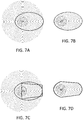
- Such a masking process is depicted in the diagrams of FIGS. 7A and 7B , where the desired elliptical shape is shown masked over the optimized coordinate set definition to create the crater design shown in FIG. 7B .
- FIGS. 7C and 7D show a similar scan path creation process using an intersect of two shapes, an ellipse and a trapezoid. The resulting shape mills slightly less area, and slightly less material, than the elliptical crater but may not be suitable for all conditions.
- the shape is asymmetrically placed around the target location 110 to provide for a single cut process with minimal extraneous milling.
- Most of the milling paths inside the depicted shape are now segments of a circle, but other versions may use straight lines or other types of curves or combinations of different lines following the principles herein.
- Those circular milling paths closest to the crater are retained as full circles in the versions of FIG. 7B and 7D .
- the segments retain all of their dwell positions and their optimized XY coordinates already provided. While the methodology of creating the crater milling patterns is described herein, the process may create these in advance and select an appropriate saved pattern for a desired target area, then apply that pattern to the desired location by calculating coordinates relative to the target area.
- the process saves the results of these optimization steps to a stream file to be accessed for controlling the ion beam when the milling is conducted.
- these several optimization parameters employed together provide a cumulative effect achieving much reduction in milling time. These factors may also be employed in any suitable sub-combination to optimize milling procedures with different requirements. Further, while a presently preferred method is given to optimize the process with respect to these parameters, other parametric models may be used and other optimization techniques may be used to achieve similar results.
- the use of multiple repetitions along each milling path provides further optimization over a single pass with longer dwell times delivering the total ion dose in one pass. This is because, while the local FIB material removal is proportional to the ion dose (total number of ions per unit area), it also depends on the ion incidence angle, with glancing angles generally having a higher mill rate. But the material removal is also off-set by the material redeposition that occurs and that is more pronounced in confined high aspect ratio structures.
- Balancing of both effects and optimization of the local net material removal is employed herein by using multiple passes, where the first pass creates a small trench with slanted walls, which then receive the next pass at a glancing angle with the effect of increasing the mill rate for those portions of the beam dwell position. Redeposition during these next passes is much less in this trench than it would be in the deep holes that are formed if the ion beam dwells at each dwell position very long, and, therefore, multiple passes allow to take maximum benefit of the aforementioned increased mill rates. This effect is quite strong on the milling rate. Typically, for silicon, the milling rate increases by a factor 6-8 when milling at 80° (glancing) instead of 0° (perpendicular). For a combined optimization effect of the overall milling time of the structure, the techniques herein tune both the ion dose in space and the beam scanning strategy to define where more material needs to be removed and to optimize the local milling rate, respectively.
- FIG. 13 shows a diagram of an example embodiment of a focused ion beam system including programming to conduct the methods herein.
- the depicted system 101 includes an evacuated envelope 10 in which is located a plasma ion source 11 including a plasma chamber with a surrounding RF antenna with RF supply 33, and impedance matching circuit 27 to transfer power to the antenna, this PFIB source providing a dense plasma for ion beam focusing column 16.
- Ion beam 18 passes from plasma source 11 through column 16 and between electrostatic deflection mechanism 20 toward specimen 22, which comprises, for example, a semiconductor device positioned on movable and tiltable X-Y stage 24 within lower chamber 26.
- a turbo-molecular pump 8 is employed for evacuating the source and maintaining high vacuum in the upper column optics region.
- the vacuum system provides within lower chamber 26 a vacuum of typically between approximately 1x10 -7 Torr (1.3 x10 -7 mbar) and 5x10 -4 Torr (6.5 x 10 -4 mbar) with nominally 10 mTorr (1.3 x10 -3 mbar) in the plasma source and ⁇ 1x10 -6 Torr (1.3 x10 -6 mbar) in the column optics chamber.
- High voltage power supply 34 may be connected to electrodes of plasma source 11 as well as to electrodes in focusing column 16 for forming an approximately 0.1 keV to 50 keV ion beam 18 and directing the same downward.
- RF power supply 33 and impedance matching circuit 27 is also provided to energize a coil of plasma ion source 11, as described above. Any other suitable known power supply or plasma chamber arrangement may be used.
- Deflection controller and amplifier 36 operated in accordance with a prescribed pattern provided by pattern generator 38, is coupled to deflection plates 20 whereby beam 18 may be controlled to trace out a corresponding pattern on the upper surface of specimen 22. In some systems, the deflection plates are placed before the final lens, as is well known in the art.
- the beam from ion plasma source 11 is brought to a focus at specimen 22 for either modifying (milling) or imaging the surface 22.
- a charged particle multiplier 40 used for detecting secondary ion or electron emission for imaging is connected to video circuit 42, the latter supplying drive for video monitor 44 also receiving deflection signals from controller 36.
- a scanning electron microscope 41, along with its power supply and controls 45, are optionally provided with the PFIB system 101.
- a gas injection nozzle 46 may be provided to inject process gasses near the sample surface.
- a sample manipulator probe 47 such as a micromanipulator, is provided in the chamber to remove the cut-free sample pillars and transfer them to a sample holder. The holder may be placed into the chamber through portal 60, and removed when a sample is loaded and to be transferred to a tomography system for examination.
- the system controller 50 may be one or more computer systems providing a user interface and processors for executing control algorithms for the various depicted parts of the system. These controls are known in the art and will not be further described here.
- the system controller 50 includes computer memory (tangible, non-transitory memory) storing program code for creating and executing the milling patterns and overall methods (workflows) described herein. As discussed above, the methods according to various embodiments, such as the example methods described with respect to FIGS.
- System controller 50 may also connect to a CAD data server or data store 52 in order to access detailed design data for semiconductor devices under test, such as the size and position of features of interest specified by an operator. Further, the system 101 may be connected via network to a larger test system controller that helps to automate sample processing.
- Emissions from each sample point are collected by charged particle multiplier 40 to create an image that is displayed on video monitor 44 by way of video circuit 42.
- Focusing optics in column 16 may comprise mechanisms known in the art for focusing or methods to be developed in the future.
- two cylindrically symmetric electrostatic lenses can be implemented to produce a de-magnified image of the round virtual source.
- embodiments can provide beam currents from about a few pico-amperes to about several micro-amperes.
- the control of the PFIB dwell-time in space opens a field of new possibilities.
- the innovation proposed to increase the material removal speed, is an optimization process based on a specific choice of number of loops and dwell time and overlap as a function of the FIB dwell position inside a crater pattern. Related optimization procedures are used in different milling patterns (rectangular mills for TEM prep). However, in the proposed innovation the optimized values for dwell time and number of loops are obtained from mathematical functions that are found to be best choices.
Landscapes
- Analytical Chemistry (AREA)
- Chemical & Material Sciences (AREA)
- Physics & Mathematics (AREA)
- Health & Medical Sciences (AREA)
- Immunology (AREA)
- Biochemistry (AREA)
- General Health & Medical Sciences (AREA)
- General Physics & Mathematics (AREA)
- Life Sciences & Earth Sciences (AREA)
- Pathology (AREA)
- Engineering & Computer Science (AREA)
- Plasma & Fusion (AREA)
- Nuclear Medicine, Radiotherapy & Molecular Imaging (AREA)
- Pulmonology (AREA)
- Radiology & Medical Imaging (AREA)
- Theoretical Computer Science (AREA)
- Sampling And Sample Adjustment (AREA)
Claims (15)
- Verfahren zum Erstellen einer Tomographieprobe aus einem Probensubstrat, Folgendes umfassend:(a) Identifizieren einer Zielfläche und eines darunterliegenden Zielvolumens des Substrats, das einen Bereich von Interesse enthält;(b) Erstellen eines Fräsmusters basierend auf der Zielfläche und einer gewünschten Höhe und einem gewünschten Radius der Probensäule;(c) Fräsen einer Mulde mit einem fokussierten lonenstrahl (focused ion beam - FIB), die asymmetrisch um die Zielfläche herum positioniert ist, um eine zylinderförmige Probensäule, die das Zielvolumen enthält, auszubilden,(i) wobei die Mulde groß genug ist, um es einem einzelnen FIB-Schnitt in einem gewünschten Winkel vertikal in Bezug auf die Ausrichtung der Probensäule zu ermöglichen, innerhalb der Mulde zu passieren und die Probensäule aus dem Substrat freizuschneiden,(ii) wobei die Mulde eine erste Tiefe auf einer Schnittseite der Probensäule von wenigstens der gewünschten Höhe der Probensäule und eine zweite, größere Tiefe gegenüber der Schnittseite aufweist, wobei die zweite Tiefe groß genug ist, um das gegenüberliegende Ende des einzelnen FIB-Schnitts aufzunehmen, um die Probensäule nach dem einzelnen FIB-Schnitt abgetrennt zu lassen, wobei die Mulde einen ersten Spalt zwischen der Probensäule und der Muldenkante auf der Schnittseite und einen zweiten Spalt, der wesentlich kleiner als der erste Spalt ist, gegenüber der Schnittseite aufweist;(d) Befestigen einer Abtastspitze eines Tastkopfs an der Probensäule;(e) Freischneiden der Säule mit dem einzelnen FIB-Schnitt in dem gewünschten Winkel; und(f) Verwenden des Tastkopfs, um die Probensäule zu einem Probenhalter zu bewegen.
- Verfahren nach Anspruch 1, wobei die Mulde eine ovale Form aufweist und das Fräsen ein Führen des FIB in einer Anzahl angrenzender gekrümmter Linien von FIB-Verweilpositionen einschließt, und wobei Verweilpositionsverweilzeiten und Anzahl der Wiederholungen pro gekrümmter Linie sich von einer äußeren Kante der Mulde zu einer inneren Kante der Mulde steigern.
- Verfahren nach dem vorhergehenden Anspruch, wobei die Verweilpositionsverweilzeiten und Anzahl der Wiederholungen pro gekrümmter Linie unter Verwendung linearer mathematischer Funktionen und der benutzerdefinierten Informationen über gezielte Probenabmessungen wie Zylinderdurchmesser und Zylinderhöhe berechnet werden.
- Verfahren nach Anspruch 2 oder 3, wobei die Verweilpositionsverweilzeiten ferner gemäß einer parabolischen Funktion für die Verweilzeit in Abhängigkeit von einer Position auf einer gegebenen kreisförmigen Linie in einem Vorlagenmuster eingestellt werden, das eine Anzahl konzentrischer Kreise umfasst, die den jeweiligen FIB-Verweilpositionen zugeordnet sind.
- Verfahren nach einem der Ansprüche 2-4, wobei die gekrümmten Linien als Liniensegmente aus einem Vorlagenmuster ausgewählt sind, das eine Anzahl konzentrischer Kreise umfasst, für die lineare und parabolische Funktionen berechnet werden.
- Verfahren nach einem der vorhergehenden Ansprüche, wobei der gewünschte Winkel für den einzelnen FIB-Schnitt ungefähr 60 Grad ist.
- Verfahren nach einem der Ansprüche 1-4, wobei der gewünschte Winkel für den einzelnen FIB-Schnitt in einem Bereich von wenigstens 55 Grad liegt.
- Verfahren nach einem der vorhergehenden Ansprüche, wobei das Fräsen automatisch gemäß einem Muster, das automatisch erzeugt wird, verrichtet wird, um das Fräsen basierend auf der Zielfläche und der gewünschten Höhe und des gewünschten Radius der Probensäule zu steuern.
- Verfahren nach einem der vorhergehenden Ansprüche, wobei die Mulde unter Verwendung eines Abtastmusters, das Linien der FIB-Verweilpositionen einschließt, gefräst wird, wobei die Linien eine radiale Überdeckung der Verweilposition (OvR) von ungefähr 80 % und eine tangentiale Überdeckung (OvT) der Verweilposition von ungefähr 70 % aufweisen.
- Verfahren nach einem der vorhergehenden Ansprüche, ferner umfassend ein Erstellen eines freigeschnittenen Fräsmusters mit einer elliptischen Verteilung von Verweilpositionsverweilzeiten über den Durchmesser des Probenzylinders hinweg und Bereitstellen des Musters, um den Schritt des Freischneidens der Säule zu steuern.
- Verfahren nach dem vorhergehenden Anspruch, wobei das freigeschnittene Fräsmuster eine Sichelform mit Kanten der Sichelform aufweist, die basierend auf dem Durchmesser des Probenzylinders berechnet wurde.
- Verfahren nach einem der vorhergehenden Ansprüche, wobei der FIB ein Plasma-FIB (PFIB) ist, der auf einer hohen Strahlstromstärke von etwa 1-2 Mikroampere für die Fräs- und Schnittvorgänge betrieben wird.
- Verfahren nach dem vorhergehenden Anspruch, wobei die Probensäule ungefähr 100 Mikrometer in der Höhe und 50 Mikrometer in dem Radius ist, und wobei die Fräs- und Schnittvorgänge in weniger als etwa 2 Stunden fertiggestellt werden.
- Verfahren nach einem der vorstehenden Ansprüche, wobei der Probenhalter ein nadelförmiger Einzelprobenhalter ist und das Verfahren ferner ein Durchführen einer Reihe tomographischer Datenabtastungen auf der Probensäule umfasst.
- lonenstrahlsystem (101) zum Anfertigen einer Probe (100), Folgendes umfassend:eine Plasmaionenquelle (11);eine lonenstrahlfokussierspalte (16), die gekoppelt ist, um Ionen aus der Plasmaionenquelle zu empfangen und sie als einen lonenstrahl in Richtung einer Vakuumkammer (26) zu fokussieren;Ablenkspulen, die in Richtung eines unteren Endes der Spalte zum Lenken des lonenstrahls bereitgestellt sind;einen bewegbaren Probentisch (24), der in der Vakuumkammer positioniert und zum Halten einer Probe angepasst ist;eine Systemsteuerung (50), die mit der Plasmaquelle, der Fokussierspalte, den Ablenkspulen und dem Probentisch wirkverbunden ist, wobei die Systemsteuerung einen greifbaren, nicht flüchtigen, einen Speicher verwahrenden Programmcode einschließt, der durch die Systemsteuerung zum Verrichten des Verfahrens nach einem der vorhergehenden Ansprüche ausführbar ist.
Priority Applications (4)
| Application Number | Priority Date | Filing Date | Title |
|---|---|---|---|
| EP16197390.4A EP3318862B1 (de) | 2016-11-04 | 2016-11-04 | Tomographieprobenvorbereitungssysteme und verfahren mit verbesserter geschwindigkeit, automatisierung und zuverlässigkeit |
| CN201710934117.0A CN108020449B (zh) | 2016-11-04 | 2017-10-10 | 具有改进的速度、自动化和可靠性的断层摄影术样品制备系统和方法 |
| KR1020170132626A KR102470232B1 (ko) | 2016-11-04 | 2017-10-12 | 개선된 속도, 자동화, 및 신뢰성을 갖는 단층 촬영 샘플 준비 시스템 및 방법 |
| US15/802,038 US10190953B2 (en) | 2016-11-04 | 2017-11-02 | Tomography sample preparation systems and methods with improved speed, automation, and reliability |
Applications Claiming Priority (1)
| Application Number | Priority Date | Filing Date | Title |
|---|---|---|---|
| EP16197390.4A EP3318862B1 (de) | 2016-11-04 | 2016-11-04 | Tomographieprobenvorbereitungssysteme und verfahren mit verbesserter geschwindigkeit, automatisierung und zuverlässigkeit |
Publications (2)
| Publication Number | Publication Date |
|---|---|
| EP3318862A1 EP3318862A1 (de) | 2018-05-09 |
| EP3318862B1 true EP3318862B1 (de) | 2019-08-21 |
Family
ID=57391762
Family Applications (1)
| Application Number | Title | Priority Date | Filing Date |
|---|---|---|---|
| EP16197390.4A Active EP3318862B1 (de) | 2016-11-04 | 2016-11-04 | Tomographieprobenvorbereitungssysteme und verfahren mit verbesserter geschwindigkeit, automatisierung und zuverlässigkeit |
Country Status (4)
| Country | Link |
|---|---|
| US (1) | US10190953B2 (de) |
| EP (1) | EP3318862B1 (de) |
| KR (1) | KR102470232B1 (de) |
| CN (1) | CN108020449B (de) |
Families Citing this family (7)
| Publication number | Priority date | Publication date | Assignee | Title |
|---|---|---|---|---|
| US10665421B2 (en) * | 2018-10-10 | 2020-05-26 | Applied Materials, Inc. | In-situ beam profile metrology |
| CN110567994B (zh) * | 2019-10-12 | 2022-03-04 | 上海华力微电子有限公司 | 一种提取用于透射电子显微镜的待测样品的方法 |
| US11837435B2 (en) * | 2020-08-19 | 2023-12-05 | Taiwan Semiconductor Manufacturing Co., Ltd. | Atom probe tomography specimen preparation |
| CN112179931B (zh) * | 2020-09-24 | 2021-10-19 | 长江存储科技有限责任公司 | 物理失效分析样品及其制备方法 |
| US11476079B1 (en) | 2021-03-31 | 2022-10-18 | Fei Company | Method and system for imaging a multi-pillar sample |
| CN113176494A (zh) * | 2021-04-23 | 2021-07-27 | 苏州鲲腾智能科技有限公司 | 一种三维存储器失效样品制备方法 |
| CN114397315B (zh) * | 2022-01-11 | 2024-05-03 | 中国矿业大学 | 一种研磨介质对煤炭破碎产物三维形貌特征影响的方法 |
Family Cites Families (11)
| Publication number | Priority date | Publication date | Assignee | Title |
|---|---|---|---|---|
| JP2005233786A (ja) * | 2004-02-19 | 2005-09-02 | Toshiba Corp | 局所分析用針状試料,試料ホルダ組立体,局所分析装置,及び局所分析用針状試料の作製方法 |
| JP4309857B2 (ja) * | 2005-02-08 | 2009-08-05 | 株式会社東芝 | 電界イオン顕微鏡又はアトムプローブに用いられる針状体の形成方法及び電界イオン顕微鏡又はアトムプローブに用いられる針状体 |
| US7442924B2 (en) * | 2005-02-23 | 2008-10-28 | Fei, Company | Repetitive circumferential milling for sample preparation |
| US8288740B2 (en) * | 2008-06-27 | 2012-10-16 | Omniprobe, Inc. | Method for preparing specimens for atom probe analysis and specimen assemblies made thereby |
| DE102011119164B4 (de) * | 2011-11-23 | 2021-01-21 | Westfälische Wilhelms-Universität Münster | Verfahren und Vorrichung zur Durchführung der Präparation wenigstens einer Probe für die Atomsonden-Tomographie |
| CN103946684B (zh) * | 2011-12-01 | 2017-06-23 | Fei 公司 | 用于横截面视图薄层的背侧打薄的高吞吐量tem制备工艺和硬件 |
| DE102012202519A1 (de) * | 2012-02-17 | 2013-08-22 | Carl Zeiss Microscopy Gmbh | Verfahren und Vorrichtungen zur Präparation mikroskopischer Proben mit Hilfe von gepulstem Licht |
| US9733164B2 (en) * | 2012-06-11 | 2017-08-15 | Fei Company | Lamella creation method and device using fixed-angle beam and rotating sample stage |
| EP2869328A1 (de) * | 2013-10-29 | 2015-05-06 | Fei Company | Differentielle Bildgebung mit Mustererkennung für die Prozessautomatisierung von Querschnittanwendungen |
| CN103743608B (zh) * | 2014-01-21 | 2016-01-20 | 东南大学 | 用于原位透射电子显微镜的深亚微米器件样品及制备方法 |
| US9281163B2 (en) | 2014-04-14 | 2016-03-08 | Fei Company | High capacity TEM grid |
-
2016
- 2016-11-04 EP EP16197390.4A patent/EP3318862B1/de active Active
-
2017
- 2017-10-10 CN CN201710934117.0A patent/CN108020449B/zh active Active
- 2017-10-12 KR KR1020170132626A patent/KR102470232B1/ko not_active Application Discontinuation
- 2017-11-02 US US15/802,038 patent/US10190953B2/en active Active
Non-Patent Citations (1)
| Title |
|---|
| None * |
Also Published As
| Publication number | Publication date |
|---|---|
| KR102470232B1 (ko) | 2022-11-23 |
| US20180143110A1 (en) | 2018-05-24 |
| CN108020449B (zh) | 2022-03-08 |
| US10190953B2 (en) | 2019-01-29 |
| EP3318862A1 (de) | 2018-05-09 |
| KR20180050209A (ko) | 2018-05-14 |
| CN108020449A (zh) | 2018-05-11 |
Similar Documents
| Publication | Publication Date | Title |
|---|---|---|
| EP3318862B1 (de) | Tomographieprobenvorbereitungssysteme und verfahren mit verbesserter geschwindigkeit, automatisierung und zuverlässigkeit | |
| US10825651B2 (en) | Automated TEM sample preparation | |
| JP6556993B2 (ja) | 断面形成用途のプロセス自動化のためのパターン認識を伴う差分画像化 | |
| CN102207472B (zh) | 用于观察特征的自动化片状铣削 | |
| US20190172680A1 (en) | Endpointing for focused ion beam processing | |
| TWI607498B (zh) | 使用帶電粒子束曝露樣品中所關注特徵的方法及系統 | |
| JP5364049B2 (ja) | 荷電粒子ビーム装置、および試料作成方法 | |
| JP2018163826A (ja) | 荷電粒子ビーム装置、試料加工方法 | |
| CN108573844B (zh) | 聚焦离子束装置的控制方法以及记录介质 | |
| EP3809447A1 (de) | Verfahren zur grossflächigen 3d-analyse von proben unter verwendung von fib-fräsen mit glanzeinfall | |
| KR102545776B1 (ko) | 백업 기점들의 동적 생성 | |
| US11282672B2 (en) | Charged particle beam apparatus and sample processing observation method | |
| CN111065907B (zh) | 试样制造装置以及试样片的制造方法 | |
| US20240120175A1 (en) | Method for preparing a microscopic sample for fib/sem tomography | |
| US20230162945A1 (en) | Method Of Imaging And Milling A Sample | |
| EP3091558B1 (de) | Adaptive abtastung zur messung der partikelgrösse unter verwendung von ausgerichteter strahlsignalanalyse | |
| JP2022009601A (ja) | 荷電粒子ビーム装置、試料加工方法 |
Legal Events
| Date | Code | Title | Description |
|---|---|---|---|
| PUAI | Public reference made under article 153(3) epc to a published international application that has entered the european phase |
Free format text: ORIGINAL CODE: 0009012 |
|
| STAA | Information on the status of an ep patent application or granted ep patent |
Free format text: STATUS: THE APPLICATION HAS BEEN PUBLISHED |
|
| AK | Designated contracting states |
Kind code of ref document: A1 Designated state(s): AL AT BE BG CH CY CZ DE DK EE ES FI FR GB GR HR HU IE IS IT LI LT LU LV MC MK MT NL NO PL PT RO RS SE SI SK SM TR |
|
| AX | Request for extension of the european patent |
Extension state: BA ME |
|
| STAA | Information on the status of an ep patent application or granted ep patent |
Free format text: STATUS: REQUEST FOR EXAMINATION WAS MADE |
|
| 17P | Request for examination filed |
Effective date: 20181026 |
|
| RBV | Designated contracting states (corrected) |
Designated state(s): AL AT BE BG CH CY CZ DE DK EE ES FI FR GB GR HR HU IE IS IT LI LT LU LV MC MK MT NL NO PL PT RO RS SE SI SK SM TR |
|
| RIN1 | Information on inventor provided before grant (corrected) |
Inventor name: AUDOIT, GUILLAME Inventor name: KWAKMAN, LAURENS Inventor name: RUE, CHAD Inventor name: DELPY, GUILLAUME PIERRE Inventor name: FILEVICH, JORGE |
|
| REG | Reference to a national code |
Ref country code: DE Ref legal event code: R079 Ref document number: 602016018898 Country of ref document: DE Free format text: PREVIOUS MAIN CLASS: G01N0001320000 Ipc: H01J0037305000 |
|
| RIC1 | Information provided on ipc code assigned before grant |
Ipc: G01N 1/06 20060101ALI20190329BHEP Ipc: H01J 37/08 20060101ALI20190329BHEP Ipc: G01N 1/32 20060101ALI20190329BHEP Ipc: G01N 1/28 20060101ALI20190329BHEP Ipc: H01J 37/305 20060101AFI20190329BHEP Ipc: H01J 37/147 20060101ALI20190329BHEP |
|
| GRAP | Despatch of communication of intention to grant a patent |
Free format text: ORIGINAL CODE: EPIDOSNIGR1 |
|
| STAA | Information on the status of an ep patent application or granted ep patent |
Free format text: STATUS: GRANT OF PATENT IS INTENDED |
|
| INTG | Intention to grant announced |
Effective date: 20190516 |
|
| GRAS | Grant fee paid |
Free format text: ORIGINAL CODE: EPIDOSNIGR3 |
|
| GRAA | (expected) grant |
Free format text: ORIGINAL CODE: 0009210 |
|
| STAA | Information on the status of an ep patent application or granted ep patent |
Free format text: STATUS: THE PATENT HAS BEEN GRANTED |
|
| AK | Designated contracting states |
Kind code of ref document: B1 Designated state(s): AL AT BE BG CH CY CZ DE DK EE ES FI FR GB GR HR HU IE IS IT LI LT LU LV MC MK MT NL NO PL PT RO RS SE SI SK SM TR |
|
| REG | Reference to a national code |
Ref country code: GB Ref legal event code: FG4D |
|
| REG | Reference to a national code |
Ref country code: CH Ref legal event code: EP |
|
| REG | Reference to a national code |
Ref country code: DE Ref legal event code: R096 Ref document number: 602016018898 Country of ref document: DE |
|
| REG | Reference to a national code |
Ref country code: AT Ref legal event code: REF Ref document number: 1170709 Country of ref document: AT Kind code of ref document: T Effective date: 20190915 |
|
| REG | Reference to a national code |
Ref country code: IE Ref legal event code: FG4D |
|
| REG | Reference to a national code |
Ref country code: LT Ref legal event code: MG4D |
|
| REG | Reference to a national code |
Ref country code: NL Ref legal event code: MP Effective date: 20190821 |
|
| PG25 | Lapsed in a contracting state [announced via postgrant information from national office to epo] |
Ref country code: FI Free format text: LAPSE BECAUSE OF FAILURE TO SUBMIT A TRANSLATION OF THE DESCRIPTION OR TO PAY THE FEE WITHIN THE PRESCRIBED TIME-LIMIT Effective date: 20190821 Ref country code: PT Free format text: LAPSE BECAUSE OF FAILURE TO SUBMIT A TRANSLATION OF THE DESCRIPTION OR TO PAY THE FEE WITHIN THE PRESCRIBED TIME-LIMIT Effective date: 20191223 Ref country code: HR Free format text: LAPSE BECAUSE OF FAILURE TO SUBMIT A TRANSLATION OF THE DESCRIPTION OR TO PAY THE FEE WITHIN THE PRESCRIBED TIME-LIMIT Effective date: 20190821 Ref country code: SE Free format text: LAPSE BECAUSE OF FAILURE TO SUBMIT A TRANSLATION OF THE DESCRIPTION OR TO PAY THE FEE WITHIN THE PRESCRIBED TIME-LIMIT Effective date: 20190821 Ref country code: NO Free format text: LAPSE BECAUSE OF FAILURE TO SUBMIT A TRANSLATION OF THE DESCRIPTION OR TO PAY THE FEE WITHIN THE PRESCRIBED TIME-LIMIT Effective date: 20191121 Ref country code: NL Free format text: LAPSE BECAUSE OF FAILURE TO SUBMIT A TRANSLATION OF THE DESCRIPTION OR TO PAY THE FEE WITHIN THE PRESCRIBED TIME-LIMIT Effective date: 20190821 Ref country code: BG Free format text: LAPSE BECAUSE OF FAILURE TO SUBMIT A TRANSLATION OF THE DESCRIPTION OR TO PAY THE FEE WITHIN THE PRESCRIBED TIME-LIMIT Effective date: 20191121 Ref country code: LT Free format text: LAPSE BECAUSE OF FAILURE TO SUBMIT A TRANSLATION OF THE DESCRIPTION OR TO PAY THE FEE WITHIN THE PRESCRIBED TIME-LIMIT Effective date: 20190821 |
|
| PG25 | Lapsed in a contracting state [announced via postgrant information from national office to epo] |
Ref country code: ES Free format text: LAPSE BECAUSE OF FAILURE TO SUBMIT A TRANSLATION OF THE DESCRIPTION OR TO PAY THE FEE WITHIN THE PRESCRIBED TIME-LIMIT Effective date: 20190821 Ref country code: GR Free format text: LAPSE BECAUSE OF FAILURE TO SUBMIT A TRANSLATION OF THE DESCRIPTION OR TO PAY THE FEE WITHIN THE PRESCRIBED TIME-LIMIT Effective date: 20191122 Ref country code: AL Free format text: LAPSE BECAUSE OF FAILURE TO SUBMIT A TRANSLATION OF THE DESCRIPTION OR TO PAY THE FEE WITHIN THE PRESCRIBED TIME-LIMIT Effective date: 20190821 Ref country code: LV Free format text: LAPSE BECAUSE OF FAILURE TO SUBMIT A TRANSLATION OF THE DESCRIPTION OR TO PAY THE FEE WITHIN THE PRESCRIBED TIME-LIMIT Effective date: 20190821 Ref country code: IS Free format text: LAPSE BECAUSE OF FAILURE TO SUBMIT A TRANSLATION OF THE DESCRIPTION OR TO PAY THE FEE WITHIN THE PRESCRIBED TIME-LIMIT Effective date: 20191221 Ref country code: RS Free format text: LAPSE BECAUSE OF FAILURE TO SUBMIT A TRANSLATION OF THE DESCRIPTION OR TO PAY THE FEE WITHIN THE PRESCRIBED TIME-LIMIT Effective date: 20190821 |
|
| REG | Reference to a national code |
Ref country code: AT Ref legal event code: MK05 Ref document number: 1170709 Country of ref document: AT Kind code of ref document: T Effective date: 20190821 |
|
| PG25 | Lapsed in a contracting state [announced via postgrant information from national office to epo] |
Ref country code: TR Free format text: LAPSE BECAUSE OF FAILURE TO SUBMIT A TRANSLATION OF THE DESCRIPTION OR TO PAY THE FEE WITHIN THE PRESCRIBED TIME-LIMIT Effective date: 20190821 |
|
| PG25 | Lapsed in a contracting state [announced via postgrant information from national office to epo] |
Ref country code: PL Free format text: LAPSE BECAUSE OF FAILURE TO SUBMIT A TRANSLATION OF THE DESCRIPTION OR TO PAY THE FEE WITHIN THE PRESCRIBED TIME-LIMIT Effective date: 20190821 Ref country code: IT Free format text: LAPSE BECAUSE OF FAILURE TO SUBMIT A TRANSLATION OF THE DESCRIPTION OR TO PAY THE FEE WITHIN THE PRESCRIBED TIME-LIMIT Effective date: 20190821 Ref country code: EE Free format text: LAPSE BECAUSE OF FAILURE TO SUBMIT A TRANSLATION OF THE DESCRIPTION OR TO PAY THE FEE WITHIN THE PRESCRIBED TIME-LIMIT Effective date: 20190821 Ref country code: RO Free format text: LAPSE BECAUSE OF FAILURE TO SUBMIT A TRANSLATION OF THE DESCRIPTION OR TO PAY THE FEE WITHIN THE PRESCRIBED TIME-LIMIT Effective date: 20190821 Ref country code: AT Free format text: LAPSE BECAUSE OF FAILURE TO SUBMIT A TRANSLATION OF THE DESCRIPTION OR TO PAY THE FEE WITHIN THE PRESCRIBED TIME-LIMIT Effective date: 20190821 Ref country code: DK Free format text: LAPSE BECAUSE OF FAILURE TO SUBMIT A TRANSLATION OF THE DESCRIPTION OR TO PAY THE FEE WITHIN THE PRESCRIBED TIME-LIMIT Effective date: 20190821 |
|
| PG25 | Lapsed in a contracting state [announced via postgrant information from national office to epo] |
Ref country code: CZ Free format text: LAPSE BECAUSE OF FAILURE TO SUBMIT A TRANSLATION OF THE DESCRIPTION OR TO PAY THE FEE WITHIN THE PRESCRIBED TIME-LIMIT Effective date: 20190821 Ref country code: SK Free format text: LAPSE BECAUSE OF FAILURE TO SUBMIT A TRANSLATION OF THE DESCRIPTION OR TO PAY THE FEE WITHIN THE PRESCRIBED TIME-LIMIT Effective date: 20190821 Ref country code: SM Free format text: LAPSE BECAUSE OF FAILURE TO SUBMIT A TRANSLATION OF THE DESCRIPTION OR TO PAY THE FEE WITHIN THE PRESCRIBED TIME-LIMIT Effective date: 20190821 Ref country code: IS Free format text: LAPSE BECAUSE OF FAILURE TO SUBMIT A TRANSLATION OF THE DESCRIPTION OR TO PAY THE FEE WITHIN THE PRESCRIBED TIME-LIMIT Effective date: 20200224 |
|
| REG | Reference to a national code |
Ref country code: DE Ref legal event code: R097 Ref document number: 602016018898 Country of ref document: DE |
|
| REG | Reference to a national code |
Ref country code: CH Ref legal event code: PL |
|
| PLBE | No opposition filed within time limit |
Free format text: ORIGINAL CODE: 0009261 |
|
| STAA | Information on the status of an ep patent application or granted ep patent |
Free format text: STATUS: NO OPPOSITION FILED WITHIN TIME LIMIT |
|
| PG2D | Information on lapse in contracting state deleted |
Ref country code: IS |
|
| PG25 | Lapsed in a contracting state [announced via postgrant information from national office to epo] |
Ref country code: CH Free format text: LAPSE BECAUSE OF NON-PAYMENT OF DUE FEES Effective date: 20191130 Ref country code: LI Free format text: LAPSE BECAUSE OF NON-PAYMENT OF DUE FEES Effective date: 20191130 Ref country code: MC Free format text: LAPSE BECAUSE OF FAILURE TO SUBMIT A TRANSLATION OF THE DESCRIPTION OR TO PAY THE FEE WITHIN THE PRESCRIBED TIME-LIMIT Effective date: 20190821 Ref country code: LU Free format text: LAPSE BECAUSE OF NON-PAYMENT OF DUE FEES Effective date: 20191104 |
|
| 26N | No opposition filed |
Effective date: 20200603 |
|
| REG | Reference to a national code |
Ref country code: BE Ref legal event code: MM Effective date: 20191130 |
|
| PG25 | Lapsed in a contracting state [announced via postgrant information from national office to epo] |
Ref country code: SI Free format text: LAPSE BECAUSE OF FAILURE TO SUBMIT A TRANSLATION OF THE DESCRIPTION OR TO PAY THE FEE WITHIN THE PRESCRIBED TIME-LIMIT Effective date: 20190821 |
|
| PG25 | Lapsed in a contracting state [announced via postgrant information from national office to epo] |
Ref country code: FR Free format text: LAPSE BECAUSE OF NON-PAYMENT OF DUE FEES Effective date: 20191130 Ref country code: IE Free format text: LAPSE BECAUSE OF NON-PAYMENT OF DUE FEES Effective date: 20191104 |
|
| PG25 | Lapsed in a contracting state [announced via postgrant information from national office to epo] |
Ref country code: BE Free format text: LAPSE BECAUSE OF NON-PAYMENT OF DUE FEES Effective date: 20191130 |
|
| PG25 | Lapsed in a contracting state [announced via postgrant information from national office to epo] |
Ref country code: CY Free format text: LAPSE BECAUSE OF FAILURE TO SUBMIT A TRANSLATION OF THE DESCRIPTION OR TO PAY THE FEE WITHIN THE PRESCRIBED TIME-LIMIT Effective date: 20190821 |
|
| GBPC | Gb: european patent ceased through non-payment of renewal fee |
Effective date: 20201104 |
|
| PG25 | Lapsed in a contracting state [announced via postgrant information from national office to epo] |
Ref country code: HU Free format text: LAPSE BECAUSE OF FAILURE TO SUBMIT A TRANSLATION OF THE DESCRIPTION OR TO PAY THE FEE WITHIN THE PRESCRIBED TIME-LIMIT; INVALID AB INITIO Effective date: 20161104 Ref country code: MT Free format text: LAPSE BECAUSE OF FAILURE TO SUBMIT A TRANSLATION OF THE DESCRIPTION OR TO PAY THE FEE WITHIN THE PRESCRIBED TIME-LIMIT Effective date: 20190821 |
|
| PG25 | Lapsed in a contracting state [announced via postgrant information from national office to epo] |
Ref country code: GB Free format text: LAPSE BECAUSE OF NON-PAYMENT OF DUE FEES Effective date: 20201104 |
|
| PG25 | Lapsed in a contracting state [announced via postgrant information from national office to epo] |
Ref country code: MK Free format text: LAPSE BECAUSE OF FAILURE TO SUBMIT A TRANSLATION OF THE DESCRIPTION OR TO PAY THE FEE WITHIN THE PRESCRIBED TIME-LIMIT Effective date: 20190821 |
|
| PGFP | Annual fee paid to national office [announced via postgrant information from national office to epo] |
Ref country code: DE Payment date: 20231120 Year of fee payment: 8 |