EP3316027A1 - Display device - Google Patents
Display device Download PDFInfo
- Publication number
- EP3316027A1 EP3316027A1 EP17198757.1A EP17198757A EP3316027A1 EP 3316027 A1 EP3316027 A1 EP 3316027A1 EP 17198757 A EP17198757 A EP 17198757A EP 3316027 A1 EP3316027 A1 EP 3316027A1
- Authority
- EP
- European Patent Office
- Prior art keywords
- display device
- display
- reflective layer
- semiconductor element
- light source
- Prior art date
- Legal status (The legal status is an assumption and is not a legal conclusion. Google has not performed a legal analysis and makes no representation as to the accuracy of the status listed.)
- Granted
Links
Images




Classifications
-
- G—PHYSICS
- G02—OPTICS
- G02F—OPTICAL DEVICES OR ARRANGEMENTS FOR THE CONTROL OF LIGHT BY MODIFICATION OF THE OPTICAL PROPERTIES OF THE MEDIA OF THE ELEMENTS INVOLVED THEREIN; NON-LINEAR OPTICS; FREQUENCY-CHANGING OF LIGHT; OPTICAL LOGIC ELEMENTS; OPTICAL ANALOGUE/DIGITAL CONVERTERS
- G02F1/00—Devices or arrangements for the control of the intensity, colour, phase, polarisation or direction of light arriving from an independent light source, e.g. switching, gating or modulating; Non-linear optics
- G02F1/01—Devices or arrangements for the control of the intensity, colour, phase, polarisation or direction of light arriving from an independent light source, e.g. switching, gating or modulating; Non-linear optics for the control of the intensity, phase, polarisation or colour
- G02F1/13—Devices or arrangements for the control of the intensity, colour, phase, polarisation or direction of light arriving from an independent light source, e.g. switching, gating or modulating; Non-linear optics for the control of the intensity, phase, polarisation or colour based on liquid crystals, e.g. single liquid crystal display cells
- G02F1/133—Constructional arrangements; Operation of liquid crystal cells; Circuit arrangements
- G02F1/1333—Constructional arrangements; Manufacturing methods
- G02F1/1335—Structural association of cells with optical devices, e.g. polarisers or reflectors
- G02F1/1336—Illuminating devices
- G02F1/133602—Direct backlight
- G02F1/133603—Direct backlight with LEDs
-
- H—ELECTRICITY
- H10—SEMICONDUCTOR DEVICES; ELECTRIC SOLID-STATE DEVICES NOT OTHERWISE PROVIDED FOR
- H10H—INORGANIC LIGHT-EMITTING SEMICONDUCTOR DEVICES HAVING POTENTIAL BARRIERS
- H10H20/00—Individual inorganic light-emitting semiconductor devices having potential barriers, e.g. light-emitting diodes [LED]
- H10H20/80—Constructional details
- H10H20/85—Packages
- H10H20/855—Optical field-shaping means, e.g. lenses
- H10H20/856—Reflecting means
-
- G—PHYSICS
- G02—OPTICS
- G02B—OPTICAL ELEMENTS, SYSTEMS OR APPARATUS
- G02B6/00—Light guides; Structural details of arrangements comprising light guides and other optical elements, e.g. couplings
- G02B6/0001—Light guides; Structural details of arrangements comprising light guides and other optical elements, e.g. couplings specially adapted for lighting devices or systems
- G02B6/0011—Light guides; Structural details of arrangements comprising light guides and other optical elements, e.g. couplings specially adapted for lighting devices or systems the light guides being planar or of plate-like form
- G02B6/0033—Means for improving the coupling-out of light from the light guide
- G02B6/0035—Means for improving the coupling-out of light from the light guide provided on the surface of the light guide or in the bulk of it
- G02B6/0045—Means for improving the coupling-out of light from the light guide provided on the surface of the light guide or in the bulk of it by shaping at least a portion of the light guide
-
- G—PHYSICS
- G02—OPTICS
- G02F—OPTICAL DEVICES OR ARRANGEMENTS FOR THE CONTROL OF LIGHT BY MODIFICATION OF THE OPTICAL PROPERTIES OF THE MEDIA OF THE ELEMENTS INVOLVED THEREIN; NON-LINEAR OPTICS; FREQUENCY-CHANGING OF LIGHT; OPTICAL LOGIC ELEMENTS; OPTICAL ANALOGUE/DIGITAL CONVERTERS
- G02F1/00—Devices or arrangements for the control of the intensity, colour, phase, polarisation or direction of light arriving from an independent light source, e.g. switching, gating or modulating; Non-linear optics
- G02F1/01—Devices or arrangements for the control of the intensity, colour, phase, polarisation or direction of light arriving from an independent light source, e.g. switching, gating or modulating; Non-linear optics for the control of the intensity, phase, polarisation or colour
- G02F1/13—Devices or arrangements for the control of the intensity, colour, phase, polarisation or direction of light arriving from an independent light source, e.g. switching, gating or modulating; Non-linear optics for the control of the intensity, phase, polarisation or colour based on liquid crystals, e.g. single liquid crystal display cells
- G02F1/133—Constructional arrangements; Operation of liquid crystal cells; Circuit arrangements
- G02F1/1333—Constructional arrangements; Manufacturing methods
- G02F1/1335—Structural association of cells with optical devices, e.g. polarisers or reflectors
- G02F1/133553—Reflecting elements
-
- G—PHYSICS
- G02—OPTICS
- G02F—OPTICAL DEVICES OR ARRANGEMENTS FOR THE CONTROL OF LIGHT BY MODIFICATION OF THE OPTICAL PROPERTIES OF THE MEDIA OF THE ELEMENTS INVOLVED THEREIN; NON-LINEAR OPTICS; FREQUENCY-CHANGING OF LIGHT; OPTICAL LOGIC ELEMENTS; OPTICAL ANALOGUE/DIGITAL CONVERTERS
- G02F1/00—Devices or arrangements for the control of the intensity, colour, phase, polarisation or direction of light arriving from an independent light source, e.g. switching, gating or modulating; Non-linear optics
- G02F1/01—Devices or arrangements for the control of the intensity, colour, phase, polarisation or direction of light arriving from an independent light source, e.g. switching, gating or modulating; Non-linear optics for the control of the intensity, phase, polarisation or colour
- G02F1/13—Devices or arrangements for the control of the intensity, colour, phase, polarisation or direction of light arriving from an independent light source, e.g. switching, gating or modulating; Non-linear optics for the control of the intensity, phase, polarisation or colour based on liquid crystals, e.g. single liquid crystal display cells
- G02F1/133—Constructional arrangements; Operation of liquid crystal cells; Circuit arrangements
- G02F1/1333—Constructional arrangements; Manufacturing methods
- G02F1/1335—Structural association of cells with optical devices, e.g. polarisers or reflectors
- G02F1/1336—Illuminating devices
- G02F1/133602—Direct backlight
- G02F1/133605—Direct backlight including specially adapted reflectors
-
- H—ELECTRICITY
- H05—ELECTRIC TECHNIQUES NOT OTHERWISE PROVIDED FOR
- H05B—ELECTRIC HEATING; ELECTRIC LIGHT SOURCES NOT OTHERWISE PROVIDED FOR; CIRCUIT ARRANGEMENTS FOR ELECTRIC LIGHT SOURCES, IN GENERAL
- H05B33/00—Electroluminescent light sources
- H05B33/02—Details
- H05B33/04—Sealing arrangements, e.g. against humidity
-
- H—ELECTRICITY
- H05—ELECTRIC TECHNIQUES NOT OTHERWISE PROVIDED FOR
- H05B—ELECTRIC HEATING; ELECTRIC LIGHT SOURCES NOT OTHERWISE PROVIDED FOR; CIRCUIT ARRANGEMENTS FOR ELECTRIC LIGHT SOURCES, IN GENERAL
- H05B33/00—Electroluminescent light sources
- H05B33/10—Apparatus or processes specially adapted to the manufacture of electroluminescent light sources
-
- H—ELECTRICITY
- H10—SEMICONDUCTOR DEVICES; ELECTRIC SOLID-STATE DEVICES NOT OTHERWISE PROVIDED FOR
- H10H—INORGANIC LIGHT-EMITTING SEMICONDUCTOR DEVICES HAVING POTENTIAL BARRIERS
- H10H20/00—Individual inorganic light-emitting semiconductor devices having potential barriers, e.g. light-emitting diodes [LED]
- H10H20/80—Constructional details
- H10H20/84—Coatings, e.g. passivation layers or antireflective coatings
- H10H20/841—Reflective coatings, e.g. dielectric Bragg reflectors
-
- H—ELECTRICITY
- H10—SEMICONDUCTOR DEVICES; ELECTRIC SOLID-STATE DEVICES NOT OTHERWISE PROVIDED FOR
- H10H—INORGANIC LIGHT-EMITTING SEMICONDUCTOR DEVICES HAVING POTENTIAL BARRIERS
- H10H20/00—Individual inorganic light-emitting semiconductor devices having potential barriers, e.g. light-emitting diodes [LED]
- H10H20/80—Constructional details
- H10H20/85—Packages
-
- H—ELECTRICITY
- H10—SEMICONDUCTOR DEVICES; ELECTRIC SOLID-STATE DEVICES NOT OTHERWISE PROVIDED FOR
- H10H—INORGANIC LIGHT-EMITTING SEMICONDUCTOR DEVICES HAVING POTENTIAL BARRIERS
- H10H20/00—Individual inorganic light-emitting semiconductor devices having potential barriers, e.g. light-emitting diodes [LED]
- H10H20/80—Constructional details
- H10H20/85—Packages
- H10H20/851—Wavelength conversion means
-
- H—ELECTRICITY
- H10—SEMICONDUCTOR DEVICES; ELECTRIC SOLID-STATE DEVICES NOT OTHERWISE PROVIDED FOR
- H10H—INORGANIC LIGHT-EMITTING SEMICONDUCTOR DEVICES HAVING POTENTIAL BARRIERS
- H10H20/00—Individual inorganic light-emitting semiconductor devices having potential barriers, e.g. light-emitting diodes [LED]
- H10H20/80—Constructional details
- H10H20/85—Packages
- H10H20/852—Encapsulations
- H10H20/853—Encapsulations characterised by their shape
-
- H—ELECTRICITY
- H10—SEMICONDUCTOR DEVICES; ELECTRIC SOLID-STATE DEVICES NOT OTHERWISE PROVIDED FOR
- H10H—INORGANIC LIGHT-EMITTING SEMICONDUCTOR DEVICES HAVING POTENTIAL BARRIERS
- H10H20/00—Individual inorganic light-emitting semiconductor devices having potential barriers, e.g. light-emitting diodes [LED]
- H10H20/80—Constructional details
- H10H20/85—Packages
- H10H20/852—Encapsulations
- H10H20/854—Encapsulations characterised by their material, e.g. epoxy or silicone resins
-
- H—ELECTRICITY
- H10—SEMICONDUCTOR DEVICES; ELECTRIC SOLID-STATE DEVICES NOT OTHERWISE PROVIDED FOR
- H10H—INORGANIC LIGHT-EMITTING SEMICONDUCTOR DEVICES HAVING POTENTIAL BARRIERS
- H10H20/00—Individual inorganic light-emitting semiconductor devices having potential barriers, e.g. light-emitting diodes [LED]
- H10H20/80—Constructional details
- H10H20/81—Bodies
- H10H20/819—Bodies characterised by their shape, e.g. curved or truncated substrates
- H10H20/82—Roughened surfaces, e.g. at the interface between epitaxial layers
-
- H—ELECTRICITY
- H10—SEMICONDUCTOR DEVICES; ELECTRIC SOLID-STATE DEVICES NOT OTHERWISE PROVIDED FOR
- H10H—INORGANIC LIGHT-EMITTING SEMICONDUCTOR DEVICES HAVING POTENTIAL BARRIERS
- H10H20/00—Individual inorganic light-emitting semiconductor devices having potential barriers, e.g. light-emitting diodes [LED]
- H10H20/80—Constructional details
- H10H20/85—Packages
- H10H20/851—Wavelength conversion means
- H10H20/8516—Wavelength conversion means having a non-uniform spatial arrangement or non-uniform concentration, e.g. patterned wavelength conversion layer or wavelength conversion layer with a concentration gradient
-
- H—ELECTRICITY
- H10—SEMICONDUCTOR DEVICES; ELECTRIC SOLID-STATE DEVICES NOT OTHERWISE PROVIDED FOR
- H10W—GENERIC PACKAGES, INTERCONNECTIONS, CONNECTORS OR OTHER CONSTRUCTIONAL DETAILS OF DEVICES COVERED BY CLASS H10
- H10W90/00—Package configurations
Definitions
- a display device main body 10a is provided to the display device 10 pertaining to the first embodiment.
- the display device main body 10a includes a display component 11 (e.g., display) for displaying images, a reflective sheet 12, an optical sheet 13, and a rear frame 14, which will all be described below.
- the display component 11 includes a liquid crystal cell, for example.
- the display component is configured to display image.
- the long side 3e of the reflective layer 3 is provided more on the arrow X1 direction side than the long side 1f of the sapphire substrate 1, and the long side 3f of the reflective layer 3 is provided more on the arrow X2 direction side than the long side 1g of the sapphire substrate 1.
- the short side 3c, the short side 3d, the long side 3e, and the long side 3f are examples of "the outer periphery of the reflective layer.”
- the short side 1d, the short side 1e, the long side 1f, and the long side 1g are examples of "the outer periphery of the semiconductor element.”
- the outer periphery of the reflective layer 3 is configured to substantially overlap the outer periphery of the sealing resin 2 (see FIG. 3 ). More specifically, in the plan view, the sealing resin 2 is configured to have a rectangular shape that includes has the short sides 2b (the arrow Z2 direction side) and 2c (the arrow Z1 direction side), and the long sides 2d (the arrow X1 direction side) and 2e (the arrow X2 direction side). Also, in the plan view, the short side 3c of the reflective layer 3 and the short side 2b of the sealing resin 2 substantially overlap. Also, in the plan view, the short side 3d of the reflective layer 3 and the short side 2c of the sealing resin 2 substantially overlap. Also, in the plan view, the long side 3e of the reflective layer 3 and the long side 2d of the sealing resin 2 substantially overlap. Also, in the plan view, the long side 3f of the reflective layer 3 and the long side 2e of the sealing resin 2 substantially overlap.
- the display device 10 is configured such that the reflective layer 3 is formed substantially flat shape. This allows the reflective layer 3 to be formed more easily.
- a display device 30 pertaining to a third embodiment will now be described through reference to FIGS. 1 to 7 .
- the phosphor layer 9 is provided to the LED element 100.
- a LED element 300 is not provided with the phosphor layer 9.
- the LED element 300 is an example of the "at least one light source" of the present disclosure.
Landscapes
- Physics & Mathematics (AREA)
- Nonlinear Science (AREA)
- General Physics & Mathematics (AREA)
- Optics & Photonics (AREA)
- Mathematical Physics (AREA)
- Chemical & Material Sciences (AREA)
- Crystallography & Structural Chemistry (AREA)
- Engineering & Computer Science (AREA)
- Manufacturing & Machinery (AREA)
- Led Device Packages (AREA)
- Devices For Indicating Variable Information By Combining Individual Elements (AREA)
Abstract
Description
- This application claims priority to Japanese Patent Application No.
2016-210490 filed on October 27, 2016 - The present invention generally relates to a display device. More specifically, the present invention relates to a display device having a light source with a reflective layer.
- Conventionally, a display device includes a light source.
JP 2006- 319371 A - Specifically, the reflective layer disclosed in
JP 2006-319371 A - With the light emitting element disclosed in
JP 2006-319371 A - One object of the present invention is to provide a display device with which a decrease in the light distribution angle can be suppressed.
- [1] In view of the state of the known technology and in accordance with an aspect of the present invention, a display device comprises a display (or a display component) and at least one light source. The display is configured to display image. The at least one light source is configured to emit light to the display. The at least one light source includes a semiconductor element with a substrate, a translucent sealing resin that covers the semiconductor element, and a reflective layer that is disposed on an upper face of the sealing resin.
With this display device, as described above, the reflective layer is disposed on the upper face of the sealing resin, which is provided to cover the semiconductor element. Thus, the surface area (plane area) of the reflective layer can be easily made larger than the surface area (plane area) of the semiconductor element. As a result, compared to when the surface area (plane area) of the reflective layer is substantially equal to the surface area (plane area) of the semiconductor element, a greater proportion of the light emitted from the semiconductor element toward the upper side of the semiconductor element is reflected to the sides of the semiconductor element by the reflective layer. This makes it possible to increase the proportion of the light emitted to the sides of the at least one light source with respect to the light emitted toward the upper side of the at least one light source. Thus, the decrease in the distribution angle of the light from the at least one light source can be suppressed. Also, by providing the reflective layer and the semiconductor element separately, there is no need to take into account the influence of heat generation from the semiconductor element and other such factors. Thus, the material of the reflective layer can be selected from a wide variety of materials. Also, by providing the reflective layer on the sealing resin, the reflective layer can be formed more easily than when the reflective layer and the semiconductor element are provided integrally. - [2] In accordance with a preferred embodiment according to the display device mentioned above, the reflective layer has an outer periphery that is disposed further outside than an outer periphery of the semiconductor element as viewed in a direction perpendicular to an upper face of the at least one light source. With this configuration, in a plan view (or as viewed in the direction perpendicular to the upper face of the at least one light source), the region occupied by the reflective layer covers the entire region occupied by the semiconductor element, and the surface area of the reflective layer is larger than the surface area of the semiconductor element. As a result, the light emitted from the semiconductor element toward the upper side of the semiconductor element can be easily reflected to all four sides of the semiconductor element by the reflective layer. This makes it possible to further increase the proportion of the light emitted to the sides of the at least one light source with respect to the light emitted toward the upper side of the at least one light source. Thus, the decrease in the distribution angle of the light from the at least one light source can be further suppressed.
- [3] In accordance with a preferred embodiment according to any one of the display devices mentioned above, the substrate is disposed at a top of the semiconductor element, and an upper face of the substrate and a lower face of the reflective layer are separated by the sealing resin. With this configuration, there is no need to form the reflective layer such that the reflective layer straddles both the upper face of the sealing resin and the upper face of the substrate. Also, there is no need to adjust the height of the upper face of the sealing resin to match with the height of the upper face of the substrate. Thus, the at least one light source can be formed more easily. Also, the substrate and the reflective layer do not interfere with each other. Thus, deterioration of the substrate and the reflective layer can be suppressed.
- [4] In accordance with a preferred embodiment according to any one of the display devices mentioned above, the reflective layer includes a specific pattern that is configured to transmit part of the light from the semiconductor element. With this configuration, part of the light from the semiconductor element can be utilized by transmitting the light to the outside of the at least one light source through the pattern of the reflection layer (the gaps in the pattern).
- [5] In accordance with a preferred embodiment according to any one of the display devices mentioned above, the specific pattern has a lattice-shape or has a shape in which rectangles are arranged in a specific direction. With this configuration, part of the light from the semiconductor element can be easily transmitted to the outside of the at least one light source.
- [6] In accordance with a preferred embodiment according to any one of the display devices mentioned above, the at least one light source further includes a phosphor layer that is disposed between the sealing resin and the semiconductor element. The phosphor layer is disposed on side faces of the semiconductor element, and overlaps the reflective layer in a plan view (as viewed in a direction perpendicular to an upper face of the at least one light source). The sealing resin and an upper face of the semiconductor element closely contact with each other. With this configuration, the phosphor layer is not disposed on the upper face of the semiconductor element, and is disposed only on the side faces of the semiconductor element. Thus, the height of the at least one light source can be reduced.
- [7] In accordance with a preferred embodiment according to any one of the display devices mentioned above, the phosphor layer is arranged to surround the side faces of the semiconductor element. With this configuration, light traveling from the side faces of the semiconductor element can be easily guided into the phosphor layer.
- [8] In accordance with a preferred embodiment according to any one of the display devices mentioned above, the sealing resin and side faces of the semiconductor element closely contact with each other. With this configuration, unlike the case when a phosphor layer or the like is provided on the side faces of the semiconductor element, etc., the at least one light source can be made smaller.
- [9] In accordance with a preferred embodiment according to any one of the display devices mentioned above, the reflective layer is formed substantially flat. With this configuration, the reflective layer can be easily formed.
- [10] In accordance with a preferred embodiment according to any one of the display devices mentioned above, the substrate is made of a sapphire substrate. The semiconductor element includes the sapphire substrate, a first conductivity type GaN layer, a light emitting layer, and a second conductivity type GaN layer that are arranged in this order from an upper face side of the sealing resin. Here, a sapphire substrate has excellent light transmittance. Therefore, if the substrate is made of a sapphire substrate, the proportion of light absorbed by the substrate can be reduced. Thus, the decrease in emission efficiency of the at least one light source can be suppressed.
- [11] In accordance with a preferred embodiment according to any one of the display devices mentioned above, the display device further comprises a reflective sheet configured to reflect light from the at least one light source. The reflective sheet includes a bottom face that is arranged substantially parallel to a display face of the display. The at least one light source is disposed at a location closer to the display than the bottom face in a direction substantially perpendicular to the display face of the display. With this configuration, the distance between the at least one light source and the display is shorter than when the at least one light source is disposed on the bottom face. Thus, the light from the at least one light source can be transmitted more efficiently to the display.
- [12] In accordance with a preferred embodiment according to any one of the display devices mentioned above, the at least one light source includes a plurality of light sources.
- [13] In accordance with a preferred embodiment according to any one of the display devices mentioned above, the light sources are arranged along a horizontal line on a plane substantially parallel to a display face of the display.
- [14] In accordance with a preferred embodiment according to any one of the display devices mentioned above, the light sources are arranged along a vertical line on a plane substantially parallel to a display face of the display.
- [15] In accordance with a preferred embodiment according to any one of the display devices mentioned above, the light sources are arranged in a plurality of lines.
- [16] In accordance with a preferred embodiment according to any one of the display devices mentioned above, the reflective layer has an outer periphery that substantially overlaps with an outer periphery of the sealing resin as viewed in a direction perpendicular to an upper face of the at least one light source.
- [17] In accordance with a preferred embodiment according to any one of the display devices mentioned above, the reflective layer has an upper face that forms an uppermost face of the at least one light source.
- [18] In accordance with a preferred embodiment according to any one of the display devices mentioned above, the substrate has an uneven upper face.
- [19] In accordance with a preferred embodiment according to any one of the display devices mentioned above, the sealing resin entirely covers the semiconductor element and the phosphor layer.
- [20] In accordance with a preferred embodiment according to any one of the display devices mentioned above, the upper face of the sealing resin is exposed to outside through a gap in the reflective layer.
- With the present invention, as described above, it is possible to provide a display device capable of suppressing the decrease in the light distribution angle.
- Referring now to the attached drawings which form a part of this original disclosure:
-
FIG. 1 is an exploded perspective view of a display device pertaining to first to fourth embodiments; -
FIG. 2 is a cross sectional view of the display device, taken along II-II line inFIG. 1 ; -
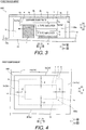
FIG. 3 is a cross sectional view of a light source of the display device pertaining to the first embodiment; -
FIG. 4 is a top plan view of the light source pertaining to the first embodiment; -
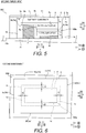
FIG. 5 is a cross sectional view of a light source of the display device pertaining to the second embodiment; -
FIG. 6 is a top plan view of the light source pertaining to the second embodiment; -
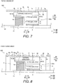
FIG. 7 is a cross sectional view of a light source of the display device pertaining to the third embodiment; -
FIG. 8 is a cross sectional view of a light source of the display device pertaining to a fourth embodiment; -
FIG. 9 is a top plan view of the light source pertaining to the fourth embodiment; -
FIG. 10 is a cross sectional view of a light source of the display device pertaining to a modification example of the first embodiment; -
FIG. 11 is an elevational view of the display device pertaining to a modification example, illustrating an arrangement of the light sources; and -
FIG. 12 is an elevational view of the display device pertaining to a modification example, illustrating another arrangement of the light sources. - Selected embodiments will now be explained with reference to the drawings. It will be apparent to those skilled in the art from this disclosure that the following descriptions of the embodiments are provided for illustration only and not for the purpose of limiting the invention as defined by the appended claims.
- First, the configuration of a display device 10 pertaining to the first embodiment will now be described through reference to
FIGS. 1 to 4 . - As shown in
FIG. 1 , a display devicemain body 10a is provided to the display device 10 pertaining to the first embodiment. The display devicemain body 10a includes a display component 11 (e.g., display) for displaying images, areflective sheet 12, anoptical sheet 13, and arear frame 14, which will all be described below. Thedisplay component 11 includes a liquid crystal cell, for example. The display component is configured to display image. In the following description, when viewed from a position facing thedisplay component 11 of the display device 10 (i.e., an elevational view), the left direction is the arrow X1 direction, the right direction is the arrow X2 direction, the front direction (toward the viewer) is the arrow Y1 direction, the rear direction is the arrow Y2 direction, the upward direction is the arrow Z1 direction, and the downward direction is the arrow Z2 direction. Also, in the illustrated embodiment, as shown inFIG. 1 , X direction represents the horizontal direction of the display device 10, Y direction represents front-to-rear direction of the display device 10, and Z direction represents the vertical direction of the display device 10. - Also, the display device 10 includes an
LED element 100 that emits light to thedisplay component 11. The display device 10 is configured as a direct-type liquid crystal module that displays video on thedisplay component 11, using as a backlight the LED (light emitting diode)element 100 provided on the arrow Y2 direction side. TheLED element 100 is an example of the "at least one light source" of the present disclosure. - As shown in
FIG. 1 , thedisplay component 11 is in the form of a plate arranged on a plane parallel to the XZ plane. Thedisplay component 11 is configured to have a rectangular shape includingshort sides long sides display component 11 includes adisplay face 11e bounded by theshort side 11a, theshort side 11b, thelong side 11c, and thelong side 11 d. - The
LED element 100 includes anLED chip 100a (seeFIG. 3 ). A plurality (ten, for example) of theLED elements 100 are provided, and they are configured to emit light on the side of the display component 11 (the arrow Y1 direction side). TheLED chip 100a is an example of the "semiconductor element" of the present disclosure. - The
reflective sheet 12 includes abottom face 12a that is arranged substantially parallel to thedisplay face 11 e of thedisplay component 11. Thedisplay face 11e of thedisplay component 11 is disposed substantially parallel to theoptical sheet 13. Also, thereflective sheet 12 includesinclined parts 12b to 12e. Theinclined parts 12b to 12e are inclined to thebottom face 12a and are provided between thebottom face 12a and the outer edges (theshort sides long sides display component 11. Theinclined parts 12b to 12e is configured to reflect (and diffuse) light from theLED element 100. Also, thereflective sheet 12 is provided between therear frame 14 and theoptical sheet 13. Thereflective sheet 12 is configured to reflect the light from theLED element 100 to the side of the display component 11 (the arrow Y1 direction side). Therear frame 14 is made of metal, for example. Therear frame 14 is formed in a concave shape recessed in the arrow Y2 direction. Also, therear frame 14 is attached to the display device 10 from the arrow Y2 direction side. - More specifically, the
reflective sheet 12 is made of a resin (preferably PET (polyethylene terephthalate) in a reflective state), for example. The reflectingsheet 12 is configured to have a shape that conforms to the rear frame 14 (a concave shape recessed toward the arrow Y2 direction side). - The
bottom face 12a of thereflective sheet 12 is formed to have a rectangular shape on a plane parallel to the XZ plane. - The
inclined parts 12b to 12e of thereflective sheet 12 extends from the edges of thebottom face 12a, respectively, to surround thebottom face 12a. Theinclined part 12b is provided between the end of thebottom face 12a on the arrow X1 direction side and theshort side 11a of thedisplay component 11, and is inclined with respect to thebottom face 12a. Like theinclined part 12b, the inclined part 12c (12d and 12e) is provided between the end of thebottom face 12a and theshort side 11b (thelong side 11c and thelong side 11 d) of thedisplay component 11, and is inclined with respect to thebottom face 12a. - Here, in the first embodiment, as shown in
FIGS. 1 and2 , theLED element 100 is disposed closer to thedisplay component 11 than thebottom face 12a in a direction (Y direction) substantially perpendicular to thedisplay face 11 e of thedisplay component 11. More specifically, the display device 10 is provided with a lightsource disposition component 15 that protrudes from thebottom face 12a toward the display component 11 (Y1 direction side). - The light
source disposition component 15 includes aninclined part 15a provided so as to be opposite theinclined part 12d, and aninclined part 15b provided so as to be opposite theinclined part 12e. The lightsource disposition component 15 includes aflat part 15c that connects the end of theinclined part 15a on the Y1 direction side with the end of theinclined part 15b on the Y1 direction side. Theflat part 15c is provided so as to extend in the X direction. TenLED elements 100 are mounted on theflat part 15c, spaced apart in the X direction. Although not depicted, a heat sink and a wiring board for the light source are provided between theflat part 15c and theLED elements 100. The lightsource disposition component 15 can be covered by thereflective sheet 12. - As shown in
FIG. 2 , the cross-sectional shape of the lightsource disposition component 15 is trapezoidal. TheLED elements 100 disposed on theflat part 15c emit light radially. InFIG. 2 , members other than thereflective sheet 12, the lightsource disposition component 15, and theLED element 100 are omitted for the sake of brevity. The broken lines inFIG. 2 are examples of the paths of light emitted from theLED element 100. - In the illustrated embodiment, the
optical sheet 13 includes a diffusion plate, a polarizing film, or the like. As shown inFIG. 1 , theoptical sheet 13 is formed in a flat shape extending in a plane parallel to the XZ plane between thedisplay component 11 and therear frame 14. Consequently, the light emitted from theLED elements 100 irradiates theoptical sheet 13. As a result, the light emitted from theLED elements 100 is diffused by theoptical sheet 13, and the polarization directions of the light are aligned by theoptical sheet 13. Theoptical sheet 13 is not limited to being configured as a single sheet, and can be a combination of a plurality of sheets each having a specific function. - The
display component 11 is configured to display images by changing the transmissivity of the liquid crystal with respect to the light transmitted through theoptical sheet 13, or the like. - Here, in the first embodiment, as shown in
FIG. 3 , theLED element 100 includes theLED chip 100a including thesapphire substrate 1. TheLED element 100 also includes atranslucent sealing resin 2 that covers theLED chip 100a. Theupper face 2a of the sealingresin 2 is formed substantially flat. TheLED element 100 includes areflective layer 3 disposed on theupper face 2a of the sealingresin 2. Thus, thereflective layer 3 forms an uppermost layer of theLED element 100. Specifically, an upper face of thereflective layer 3 forms an uppermost face of theLED element 100. More specifically, theupper face 2a of the sealingresin 2 is formed to be substantially parallel to theflat part 15c of the lightsource disposition component 15. Thesapphire substrate 1 and theupper face 2a are examples of the "substrate" and the "upper face of the sealing resin," respectively, of the present disclosure. The phrase "theupper face 2a is formed substantially flat" is a broad concept encompassing a case in which fine bumps or pits are formed on theupper face 2a of the sealingresin 2. - Of the light emitted from the
LED chip 100a (a PN junction 5 (discussed below)), the light emitted toward the upper side of theLED chip 100a is incident on thereflective layer 3, and is reflected to the sides of theLED chip 100a, or to the lower side of thereflective layer 3. - Also, the
lower face 3a of thereflective layer 3 has an uneven shape. More specifically, a plurality oftiny protrusions 3b are disposed on thelower face 3a of thereflective layer 3. Theprotrusions 3b protrude so as to taper toward the arrow Y2 direction side. Thelower face 3a is an example of the "lower face of the reflective layer" of the present disclosure. - The
upper face 1a of thesapphire substrate 1 also has an uneven shape. More specifically, a plurality oftiny protrusions 1b are disposed on theupper face 1a of thesapphire substrate 1. In other words, theupper face 1a of thesapphire substrate 1 is formed as an uneven upper face. Theprotrusions 1b protrude toward the arrow Y1 direction side. Theprotrusions 1b are formed by electric discharge machining. Theupper face 1a is an example of the "upper face of the substrate" of the present disclosure. - The
reflective layer 3 is made of gold. More specifically, thereflective layer 3 is provided by vapor-depositing gold on theupper face 2a of the sealingresin 2. - Also, in the first embodiment, the
reflective layer 3 is formed substantially flat. More specifically, thereflective layer 3 is configured so that its thickness in the Y direction is substantially constant. The phrase "thereflective layer 3 is formed substantially flat" is a broad concept encompassing a case in which fine bumps or pits are formed on thelower face 3a of thereflective layer 3. - In the first embodiment, the
LED chip 100a includes thesapphire substrate 1, an N-type GaN layer 4, thePN junction 5, and a P-type GaN layer 6 that are disposed in this order starting from theupper face 2a side of the sealing resin 2 (the arrow Y1 direction side). That is, in theLED chip 100a, thesapphire substrate 1 is disposed on the uppermost face. In other words, thesapphire substrate 1 is disposed at a top of theLED chip 100a. That is, theLED chip 100a is a flip chip type. More specifically, the N-type GaN layer 4 is formed under thelower face 1c of thesapphire substrate 1. Also, a steppedpart 4b extending in the Y direction (as viewed from the X direction) is provided to thelower face 4a of the N-type GaN layer 4. Aflat face 4c and aflat face 4d are provided to thelower face 4a of the N-type GaN layer 4, with the steppedpart 4b as a boundary. Theflat face 4c is substantially flat and parallel relative to the XZ plane, and extends in the Z2 direction relative to the steppedpart 4b. Theflat face 4d is substantially flat and parallel relative to the XZ plane, and extends in the Z1 direction relative to the steppedpart 4b. ThePN junction 5 is formed under theflat face 4d of the N-type GaN layer 4. Anegative electrode pad 7 is provided under theflat face 4c of the N-type GaN layer 4. The P-type GaN layer 6 is formed under thePN junction 5. Apositive electrode pad 8 is provided under the P-type GaN layer 6. Also, thepositive electrode pad 8 and thenegative electrode pad 7 are in contact with (soldered to) and electrically connected to a copper foil (not shown) on theflat part 15c of the lightsource disposition component 15. ThePN junction 5 is an example of the "light emitting layer" of the present disclosure. The N-type GaN layer 4 and the P-type GaN layer 6 are examples of the "first conductivity type GaN layer" and the "second conductivity type GaN layer," respectively, of the present disclosure. - Also, in the first embodiment, as shown in
FIG. 4 , thereflective layer 3 has an outer periphery that is disposed further to the outside than an outer periphery of theLED chip 100a as viewed in a direction perpendicular to an upper face of theLED element 100 or in the Y direction (hereinafter "in the plan view"). More specifically, in the plan view, thereflective layer 3 is configured to have a rectangular shape that includes theshort sides 3c (the arrow Z2 direction side) and 3d (the arrow Z1 direction side), and thelong sides 3e (the arrow X1 direction side) and 3f (the arrow X2 direction side). In the plan view, thesapphire substrate 1 is configured to have a rectangular shape that includes theshort sides 1d (the arrow Z2 direction side) and 1e (the arrow Z1 direction side), and thelong sides 1f (the arrow X1 direction side) and 1g (the arrow X2 direction side). Theshort side 3c of thereflective layer 3 is provided more on the arrow Z2 direction side than theshort side 1d of thesapphire substrate 1, and theshort side 3d of thereflective layer 3 is provided more on the arrow Z1 direction side thanshort side 1e of thesapphire substrate 1. Thelong side 3e of thereflective layer 3 is provided more on the arrow X1 direction side than thelong side 1f of thesapphire substrate 1, and thelong side 3f of thereflective layer 3 is provided more on the arrow X2 direction side than thelong side 1g of thesapphire substrate 1. Theshort side 3c, theshort side 3d, thelong side 3e, and thelong side 3f are examples of "the outer periphery of the reflective layer." Theshort side 1d, theshort side 1e, thelong side 1f, and thelong side 1g are examples of "the outer periphery of the semiconductor element." - In the plan view, the outer periphery of the
reflective layer 3 is configured to substantially overlap the outer periphery of the sealing resin 2 (seeFIG. 3 ). More specifically, in the plan view, the sealingresin 2 is configured to have a rectangular shape that includes has theshort sides 2b (the arrow Z2 direction side) and 2c (the arrow Z1 direction side), and thelong sides 2d (the arrow X1 direction side) and 2e (the arrow X2 direction side). Also, in the plan view, theshort side 3c of thereflective layer 3 and theshort side 2b of the sealingresin 2 substantially overlap. Also, in the plan view, theshort side 3d of thereflective layer 3 and theshort side 2c of the sealingresin 2 substantially overlap. Also, in the plan view, thelong side 3e of thereflective layer 3 and thelong side 2d of the sealingresin 2 substantially overlap. Also, in the plan view, thelong side 3f of thereflective layer 3 and thelong side 2e of the sealingresin 2 substantially overlap. - In the first embodiment, as shown in
FIG. 3 , theupper face 1a of thesapphire substrate 1 and thelower face 3a of thereflective layer 3 are configured to be separated from each other by the sealingresin 2. More specifically, the entireupper face 1a of thesapphire substrate 1 is covered by the sealingresin 2. Thus, the sapphire substrate 1 (theupper face 1a) does not directly contact with the reflective layer 3 (thelower face 3a). - Also, in the first embodiment, the
LED element 100 further includes aphosphor layer 9 that is disposed between the sealingresin 2 and theLED chip 100a. Thephosphor layer 9 is disposed on the side faces of theLED chip 100a. Also, thephosphor layer 9 is disposed so as to overlap thereflective layer 3 in the plan view. The sealingresin 2 and theupper face 1a of theLED chip 100a (the sapphire substrate 1) closely contact with each other. More specifically, thephosphor layer 9 is disposed so as to cover the entire surface of theLED chip 100a other than theupper face 1a of thesapphire substrate 1. Also, theentire phosphor layer 9 is disposed inside the sealingresin 2. Specifically, the sealingresin 2 entirely covers theLED chip 100a and thephosphor layer 9. - In the first embodiment, as shown in
FIG. 4 , thephosphor layer 9 is arranged to surround the side faces of theLED chip 100a. More specifically, in the plan view, thephosphor layer 9 with a thickness t1 is disposed to closely contact with theshort side 1d, theshort side 1e, thelong side 1f, and thelong side 1g of theLED chip 100a (the sapphire substrate 1). - The following effects can be obtained with the first embodiment.
- As described above, in the first embodiment, the display device 10 comprises the
display component 11 for displaying images and theLED elements 100 for emitting light at thedisplay component 11. TheLED elements 100 each include anLED chip 100a. TheLED chip 100a includes thesapphire substrate 1, thetranslucent sealing resin 2 that covers theLED chip 100a, and thereflective layer 3 disposed on theupper face 2a of the sealingresin 2. Thus, thereflective layer 3 is disposed on theupper face 2a of the sealingresin 2 that is provided so as to cover theLED chips 100a. Thus, the surface area (plane area) of thereflective layer 3 can be easily made larger than the surface area (plane area) of theLED chips 100a. As a result, compared to when the surface area (plane area) of thereflective layer 3 is substantially equal to the surface area (plane area) of theLED chips 100a, a greater proportion of the light emitted from theLED chips 100a to the upper side of theLED chip 100a is reflected by thereflective layer 3 toward the sides of theLED chips 100a. Consequently, the proportion of the light emitted to the sides of theLED element 100 can be increased with respect to the light emitted to the upper side of theLED element 100. Thus, the decrease in the distribution angle of the light from theLED element 100 can be suppressed. Also, by providing thereflective layer 3 and theLED chip 100a separately, there is no need to take into account the influence of heat generation or the like in theLED chip 100a. Thus, the material of thereflective layer 3 can be selected from a wider range. Also, by providing thereflective layer 3 on the sealingresin 2, thereflective layer 3 can be formed more easily than when thereflective layer 3 and theLED chip 100a are provided integrally. Note that the phrase "theupper face 2a is formed substantially flat" is a broad concept encompassing a case in which fine bumps or pits are formed on theupper face 2a of the sealingresin 2. - In the first embodiment, as described above, the display device 10 is configured such that the outer periphery of the
reflective layer 3 is disposed more to the outside than the outer periphery of theLED chip 100a in the plan view. Consequently, in the plan view, the region occupied by thereflective layer 3 covers the entire region occupied by theLED chip 100a, and the surface area of thereflective layer 3 is larger than the surface area of theLED chip 100a. As a result, the light emitted from theLED chip 100a to the upper side of theLED chip 100a can be easily reflected by thereflective layer 3 to all four sides of theLED chip 100a. Consequently, the proportion of the light emitted to the sides of theLED element 100 can be further increased with respect to the light emitted to the upper side of theLED element 100. Thus, the decrease in the distribution angle of the light from theLED element 100 can be further suppressed. - In the first embodiment, as described above, the display device 10 is configured such that the
reflective layer 3 has the outer periphery that substantially overlaps the outer periphery of the sealingresin 2 in the plan view. Consequently, the light passing near the edges of the sealingresin 2 can be reflected by thereflective layer 3. Thus, the light from theLED chip 100a can be easily reflected to the sides of theLED element 100. - Also, in the first embodiment, as described above, the display device 10 is configured such that the
sapphire substrate 1 of theLED chip 100a is disposed on the uppermost surface (at the top of theLED chip 100a), and theupper face 1a of thesapphire substrate 1 and thelower face 3a of thereflective layer 3 are separated from each other by the sealingresin 2. Consequently, there is no need to adjust the height of the sealingresin 2 so that thereflective layer 3 will straddle both theupper face 1a of thesapphire substrate 1 and theupper face 2a of the sealingresin 2 to the side of thesapphire substrate 1. Thus, theLED element 100 can be formed more easily. Also, thesapphire substrate 1 and thereflective layer 3 do not interfere with each other. Thus, degradation of thesapphire substrate 1 and thereflective layer 3 can be suppressed. - In the first embodiment, as described above, the display device 10 is configured such that the
LED element 100 further includes thephosphor layer 9 that is disposed between the sealingresin 2 and theLED chip 100a. Thephosphor layer 9 is disposed on the side faces of theLED chip 100a, and is disposed so as to overlap thereflective layer 3 in the plan view. The sealingresin 2 and theupper face 1a of theLED chip 100a (the sapphire substrate 1) closely contact with each other. Consequently, thephosphor layer 9 is not disposed on theupper face 1a of theLED chip 100a (the sapphire substrate 1), and thephosphor layer 9 is disposed only on the side faces of theLED chip 100a. Thus, the height of theLED element 100 can be reduced. - In the first embodiment, as described above, the display device 10 is configured such that the
phosphor layer 9 is arranged to surround the side faces of theLED chip 100a. Consequently, the light traveling from the side faces of theLED chip 100a can easily be introduced into thephosphor layer 9. - In the first embodiment, as described above, the display device 10 is configured such that the
lower face 3a of thereflective layer 3 has an uneven shape. Consequently, the light emitted from theLED chip 100a and incident on thelower face 3a of thereflective layer 3 is diffused by the convex and the concave (or the texturing) on thereflective layer 3. Thus, the proportion of the light reflected to the sides of theLED chip 100a can be effectively increased. - In the first embodiment, as described above, the display device 10 is configured such that the
upper face 1a of thesapphire substrate 1 has an uneven shape. Consequently, the light emitted from theLED chip 100a is diffused by the convex and concave (or texturing) on thesapphire substrate 1. Thus, the proportion of the light emitted to the sides of theLED element 100 can be effectively increased. - In the first embodiment, as described above, the display device 10 is configured such that the
reflective layer 3 includes gold. Gold has excellent resistance to heat and humidity (heat resistance and corrosion resistance). Therefore, if thereflective layer 3 includes gold, the resistance of thereflective layer 3 to heat and humidity (heat resistance and corrosion resistance) can be improved. - In the first embodiment, as described above, the display device 10 is configured such that the
reflective layer 3 is formed substantially flat shape. This allows thereflective layer 3 to be formed more easily. - In the first embodiment, as described above, the display device 10 is configured such that the substrate includes the
sapphire substrate 1, and theLED chip 100a includes thesapphire substrate 1, the N-type GaN layer 4, thePN junction 5, and the P-type GaN layer 6 that are disposed in this order starting from theupper face 2a side of the sealingresin 2. Thesapphire substrate 1 here has excellent translucency. Therefore, if the substrate includes thesapphire substrate 1, the proportion of light absorbed by the substrate can be decreased. Thus, the decrease in the emission efficiency of theLED element 100 can be suppressed. - In the first embodiment, as described above, the display device 10 is configured to include the
LED chips 100a that are disposed on the rear face side of the display devicemain body 10a. TheLED chips 100a are covered by the sealingresin 2. Thereflective layer 3 is disposed on theupper face 2a of the sealingresin 2. The light emitted from theLED chips 100a is reflected by thereflective layer 3. Thereflective layer 3 is disposed on theupper face 2a of the sealingresin 2 that is provided to cover theLED chips 100a. Thus, the surface area (plane area) of thereflective layer 3 can be easily made larger than the surface area (plane area) of theLED chips 100a. As a result, the greater proportion of the light emitted from theLED chips 100a toward the upper side of theLED chips 100a is reflected to the sides of theLED chips 100a by thereflective layer 3 as compared to when the surface area (plane area) of thereflective layer 3 is substantially equal to the surface area (plane area) of theLED chips 100a. Consequently, the proportion of the light emitted to the sides of theLED element 100 can be increased with respect to the light emitted to the upper side of theLED element 100. Thus, the decrease in the distribution angle of light from theLED element 100 can be suppressed. As a result, it is possible to widen the irradiation range of light emitted by theLED element 100. Therefore, the occurrence of uneven brightness in thedisplay component 11 of the display devicemain body 10a can be suppressed. - In the first embodiment, as described above, the display device 10 is configured such that the
LED element 100 is disposed at a location closer to thedisplay component 11 than thebottom face 12a in a direction substantially perpendicular to thedisplay face 11e of thedisplay component 11. Consequently, compared to when theLED element 100 is disposed on thebottom face 12a, the distance between theLED element 100 and thedisplay component 11 can become shorter. Thus, the light from theLED element 100 can be transmitted more efficiently to thedisplay component 11. - Next, the configuration of a display device 20 pertaining to a second embodiment will now be described through reference to
FIGS. 5 and 6 . The display device 10 in the first embodiment includes theLED element 100 in which thesapphire substrate 1 and thereflective layer 3 are separated. On the other hand, the display device 20 in the second embodiment differs from the display device 10 in the first embodiment in that the display device 20 includes anLED element 200 in which thesapphire substrate 1 and thereflective layer 3 closely contact with each other. Those components that have the same configuration as in the first embodiment above are labeled the same in the drawings. TheLED element 200 is an example of the "at least one light source" of the present disclosure. - In the second embodiment, as shown in
FIG. 5 , the configuration is such that theupper face 1a of thesapphire substrate 1 and thelower face 3a of thereflective layer 3 closely or directly contact with each other. More specifically, the sealingresin 2 is not interposed between theupper face 1a of thesapphire substrate 1 and thelower face 3a of thereflective layer 3. - As shown in
FIG. 6 , in the plan view, aphosphor layer 19 with a thickness t2 is disposed so as to closely contact with theshort side 1d, theshort side 1e, thelong side 1f, and thelong side 1g of theLED chip 100a (the sapphire substrate 1). The thickness t2 is less than the thickness t1 (seeFIG. 4 ). - The rest of the configuration of the second embodiment is the same as in the first embodiment.
- In the second embodiment, as described above, the display device 20 is configured such that the
LED chip 100a includes thesapphire substrate 1 that is disposed on the uppermost face (or at the top of theLED chip 100a), and theupper face 1a of thesapphire substrate 1 and thelower face 3a of thereflective layer 3 closely contact with each other. Consequently, the sealingresin 2 is not interposed between theupper face 1a of thesapphire substrate 1 and thelower face 3a of thereflective layer 3. Thus, the light emitted from theLED chip 100a to the upper side is less likely to be absorbed by the sealingresin 2. As a result, the decrease in the emission efficiency of theLED element 200 can be suppressed. - The other effects of the second embodiment are the same as in the first embodiment.
- The configuration of a display device 30 pertaining to a third embodiment will now be described through reference to
FIGS. 1 to 7 . With the display device 10 in the first embodiment, thephosphor layer 9 is provided to theLED element 100. On the other hand, with the display device 30 in this third embodiment, aLED element 300 is not provided with thephosphor layer 9. Those components that have the same configuration as in the first embodiment above are labeled the same in the drawings. TheLED element 300 is an example of the "at least one light source" of the present disclosure. - In the third embodiment, as shown in
FIG. 7 , the side faces of theLED chip 100a and the sealingresin 2 closely or directly contact with each other. More specifically, thephosphor layer 9 is not interposed between the side faces ofLED chip 100 and the sealingresin 2. More precisely, in the illustrated embodiment, the display device 30 includes an optical sheet 23 (seeFIG. 1 ) with quantum dots. With this configuration, the color of the light emitted from theLED chips 100a changes when the light is incident on theoptical sheet 23. - The rest of the configuration of the third embodiment is the same as in the first embodiment above.
- The following effect can be obtained with the third embodiment.
- In the third embodiment, as described above, the display device 30 is configured such that the side faces of the
LED chip 100 and the sealingresin 2 closely contact with each other. Consequently, unlike when thephosphor layer 9 or the like is provided to the side faces of theLED chip 100a, theLED element 300 can be made smaller. - The other effects of the third embodiment are the same as in the first embodiment above.
- The configuration of a display device 40 pertaining to a fourth embodiment will now be described through reference to
FIGS. 8 and9 . With the display device 40 in this fourth embodiment, unlike in the first embodiment, a pattern is formed on areflective layer 33 of anLED element 400. Those components that have the same configuration as in the first embodiment above are labeled the same in the drawings. TheLED element 400 is an example of the "at least one light source" of the present disclosure. - In the fourth embodiment, as shown in
FIG. 8 , thereflective layer 33 includes a specific pattern that transmits part of the light from theLED chips 100a. More specifically,grooves 33a are formed by removing part of thereflective layer 33, and the sealingresin 2 is exposed outside from thegrooves 33a. Thus, theupper face 2a of the sealingresin 2 exposes outside through gaps (grooves 33a) in thereflective layer 33. - In the fourth embodiment, as shown in
FIG. 9 , the specific pattern has a shape in which rectangles are arranged in the Z direction. More specifically, in the plan view, thegrooves 33a extend in the X direction from thelong side 2d of the sealingresin 2 to thelong side 2e. More precisely, the configuration is such that in the plan view thereflective layer 33 and thegrooves 33a arranged in a continuously alternating pattern. The Z direction is an example of the "specific direction" of the present disclosure. - The rest of the configuration of the fourth embodiment is the same as in the first embodiment above.
- The following effect can be obtained with the fourth embodiment.
- With the fourth embodiment, as described above, the display device 40 is configured such that the
reflective layer 33 includes a specific pattern that transmits part of the light from theLED chips 100a. Consequently, part of the light from theLED chips 100a can be utilized by being transmitted to the outside of theLED element 400 through the pattern of the reflective layer 33 (the gaps in the pattern). - With the fourth embodiment, as described above, the display device 40 is configured such that a specific pattern has a shape in which rectangles are arranged in the Z direction. Consequently, part of the light from the
LED chips 100a can be easily transmitted to the outside of theLED element 400. - The other effects of the fourth embodiment are the same as in the first embodiment above.
- The embodiments disclosed herein are just examples in every respect, and should not be interpreted as being limiting in nature. The scope of the invention being indicated by the appended claims rather than by the above description of the embodiments, all modifications (modification examples) within the meaning and range of the claims are included.
- For example, in the first embodiment, the
LED chips 100a are a flip-chip type in which thesapphire substrate 1 is disposed on the uppermost surface (at the top of the LED element 100). However, the present invention is not limited to or by this. For example, as shown inFIG. 10 , theLED chip 100a can be a lateral chip type in which thesapphire substrate 1 is disposed on the lowermost surface (at the bottom of the LED element 100). In this case, thenegative electrode pad 7 and thepositive electrode pad 8 are connected by wires (not shown) to the copper foil (not shown) on theflat part 15c of the lightsource disposition component 15. TheLED chips 100a in the second to fourth embodiments can also be a lateral chip type. - Also, in the first to fourth embodiments above, the light source includes the LED element 100 (200, 300, 400). However, the present invention is not limited to or by this. For example, the light source can be an element other than an LED element.
- Also, in the fourth embodiment, the
reflective layer 33 has a shape in which rectangles are arranged in the Z direction. However, the present invention is not limited to or by this. For example, thereflective layer 33 can have a lattice shape. Specifically, in this case, thereflective layer 33 can include crisscrossing strips arranged horizontally and vertically, or a sheet-like member with apertures spaced part with each other. - Also, in the first and fourth embodiments, the
phosphor layer 9 is disposed only on the side faces of theLED chips 100a. However, the present invention is not limited to or by this. For example, thephosphor layer 9 can also be provided on the upper faces 1a of theLED chips 100a (the sapphire substrate 1). - Also, in the first to fourth embodiments, the
upper face 1a of thesapphire substrate 1 has an uneven shape. However, the invention is not limited to or by this. For example, thelower face 1c of thesapphire substrate 1 can have an uneven shape. Also, each of theupper face 1a and thelower face 1c of thesapphire substrate 1 can have an uneven shape. - Also, in the first to fourth embodiments, the reflective layer 3 (33) is formed from gold. However, the present invention is not limited to or by this. For example, the reflective layer 3 (33) can be formed from silver.
- Also, in the first to fourth embodiments, in the plan view, the reflective layer 3 (33) (the LED element 100 (200, 300, 400)) and the sapphire substrate 1 (the
LED chips 100a) are each rectangular in shape. However, the present invention is not limited to or by this. For example, the reflective layer 3 (33) (the LED element 100 (200, 300, 400)) and the sapphire substrate 1 (theLED chips 100a) can each have a square shape. - Also, in the first to fourth embodiments, the
protrusions 1b (protrusions 3b) protrudes so as to taper toward the arrow Y1 (Y2) direction side. However, the present invention is not limited to or by this. For example, theprotrusions 1b (protrusions 3b) can have a spherical surface. - As shown in
FIG. 1 , the display device 10 (20, 30, 40) includes the plurality of the LED elements 100 (200, 300, 400). The LED elements 100 (200, 300, 400) are arranged along a horizontal line (along the X direction) on a plane substantially parallel to thedisplay face 11e of the display component 11 (XZ plane). However, as shown inFIG. 11 , the LED elements 100 (200, 300, 400) can be arranged along a vertical line (along the Z direction) on a plane substantially parallel to thedisplay face 11e of the display component 11 (XZ plane). Also, as shown inFIG. 12 , the LED elements 100 (200, 300, 400) can be arranged in a plurality of lines. - In understanding the scope of the present invention, the term "comprising" and its derivatives, as used herein, are intended to be open ended terms that specify the presence of the stated features, elements, components, groups, integers, and/or steps, but do not exclude the presence of other unstated features, elements, components, groups, integers and/or steps. The foregoing also applies to words having similar meanings such as the terms, "including", "having" and their derivatives. Also, the terms "part," "section," "portion," "member" or "element" when used in the singular can have the dual meaning of a single part or a plurality of parts unless otherwise stated.
- As used herein, the following directional terms "forward", "rearward", "front", "rear", "up", "down", "above", "below", "upward", "downward", "top", "bottom", "side", "vertical", "horizontal", "perpendicular" and "transverse" as well as any other similar directional terms refer to those directions of a display device in an upright position. Accordingly, these directional terms, as utilized to describe the display device should be interpreted relative to a display device in an upright position on a horizontal surface. The terms "left" and "right" are used to indicate the "right" when referencing from the right side as viewed from the front of the display device, and the "left" when referencing from the left side as viewed from the front of the display device.
- The term "attached" or "attaching", as used herein, encompasses configurations in which an element is directly secured to another element by affixing the element directly to the other element; configurations in which the element is indirectly secured to the other element by affixing the element to the intermediate member(s) which in turn are affixed to the other element; and configurations in which one element is integral with another element, i.e. one element is essentially part of the other element. This definition also applies to words of similar meaning, for example, "joined", "connected", "coupled", "mounted", "bonded", "fixed" and their derivatives. Finally, terms of degree such as "substantially", "about" and "approximately" as used herein mean an amount of deviation of the modified term such that the end result is not significantly changed.
- While only selected embodiments have been chosen to illustrate the present invention, it will be apparent to those skilled in the art from this disclosure that various changes and modifications can be made herein without departing from the scope of the invention as defined in the appended claims. For example, unless specifically stated otherwise, the size, shape, location or orientation of the various components can be changed as needed and/or desired so long as the changes do not substantially affect their intended function. Unless specifically stated otherwise, components that are shown directly connected or contacting each other can have intermediate structures disposed between them so long as the changes do not substantially affect their intended function. The functions of one element can be performed by two, and vice versa unless specifically stated otherwise. The structures and functions of one embodiment can be adopted in another embodiment. It is not necessary for all advantages to be present in a particular embodiment at the same time. Every feature which is unique from the prior art, alone or in combination with other features, also should be considered a separate description of further inventions by the applicant, including the structural and/or functional concepts embodied by such feature(s). Thus, the foregoing descriptions of the embodiments according to the present invention are provided for illustration only, and not for the purpose of limiting the invention as defined by the appended claims.
Claims (15)
- A display device comprising:a display configured to display image; andat least one light source configured to emit light to the display, the at least one light source includinga semiconductor element with a substrate,a translucent sealing resin that covers the semiconductor element, anda reflective layer that is disposed on an upper face of the sealing resin.
- The display device according to claim 1, wherein
the reflective layer has an outer periphery that is disposed further outside than an outer periphery of the semiconductor element as viewed in a direction perpendicular to an upper face of the at least one light source. - The display device according to claim 1 or 2, wherein
the substrate is disposed at a top of the semiconductor element, and
an upper face of the substrate and a lower face of the reflective layer are separated by the sealing resin. - The display device according to any one of claims 1 to 3, wherein
the reflective layer includes a specific pattern that is configured to transmit part of the light from the semiconductor element. - The display device according to claim 4, wherein
the specific pattern has a lattice-shape or has a shape in which rectangles are arranged in a specific direction. - The display device according to any one of claims 1 to 5, wherein
the at least one light source further includes a phosphor layer that is disposed between the sealing resin and the semiconductor element,
the phosphor layer is disposed on side faces of the semiconductor element, and overlaps the reflective layer as viewed in a direction perpendicular to an upper face of the at least one light source, and
the sealing resin and an upper face of the semiconductor element closely contact with each other. - The display device according to claim 6, wherein
the phosphor layer is arranged to surround the side faces of the semiconductor element. - The display device according to any one of claims 1 to 5, wherein
the sealing resin and side faces of the semiconductor element closely contact with each other. - The display device according to any one of claims 1 to 8, wherein
the reflective layer is formed substantially flat. - The display device according to any one of claims 1 to 9, wherein
the substrate is made of a sapphire substrate, and
the semiconductor element includes the sapphire substrate, a first conductivity type GaN layer, a light emitting layer and a second conductivity type GaN layer that are arranged in this order starting from an upper face side of the sealing resin. - The display device according to any one of claims 1 to 10, further comprising
a reflective sheet configured to reflect light from the at least one light source, the reflective sheet including a bottom face that is arranged substantially parallel to a display face of the display,
the at least one light source being disposed at a location closer to the display than the bottom face in a direction substantially perpendicular to the display face of the display. - The display device according to any one of claims 1 to 11, wherein
the at least one light source includes a plurality of light sources. - The display device according to claim 12, wherein
the light sources are arranged along a horizontal line on a plane substantially parallel to a display face of the display. - The display device according to claim 12 or 13, wherein
the light sources are arranged along a vertical line on a plane substantially parallel to a display face of the display. - The display device according to any one of claims 12 to 14, wherein
the light sources are arranged in a plurality of lines.
Priority Applications (2)
| Application Number | Priority Date | Filing Date | Title |
|---|---|---|---|
| EP20208450.5A EP3800674A1 (en) | 2016-10-27 | 2017-10-27 | Light source |
| EP19151492.6A EP3489744B1 (en) | 2016-10-27 | 2017-10-27 | Display device |
Applications Claiming Priority (1)
| Application Number | Priority Date | Filing Date | Title |
|---|---|---|---|
| JP2016210490A JP6932910B2 (en) | 2016-10-27 | 2016-10-27 | Display device |
Related Child Applications (3)
| Application Number | Title | Priority Date | Filing Date |
|---|---|---|---|
| EP19151492.6A Division EP3489744B1 (en) | 2016-10-27 | 2017-10-27 | Display device |
| EP19151492.6A Division-Into EP3489744B1 (en) | 2016-10-27 | 2017-10-27 | Display device |
| EP20208450.5A Division EP3800674A1 (en) | 2016-10-27 | 2017-10-27 | Light source |
Publications (2)
| Publication Number | Publication Date |
|---|---|
| EP3316027A1 true EP3316027A1 (en) | 2018-05-02 |
| EP3316027B1 EP3316027B1 (en) | 2020-07-29 |
Family
ID=60190691
Family Applications (3)
| Application Number | Title | Priority Date | Filing Date |
|---|---|---|---|
| EP17198757.1A Active EP3316027B1 (en) | 2016-10-27 | 2017-10-27 | Display device |
| EP20208450.5A Withdrawn EP3800674A1 (en) | 2016-10-27 | 2017-10-27 | Light source |
| EP19151492.6A Active EP3489744B1 (en) | 2016-10-27 | 2017-10-27 | Display device |
Family Applications After (2)
| Application Number | Title | Priority Date | Filing Date |
|---|---|---|---|
| EP20208450.5A Withdrawn EP3800674A1 (en) | 2016-10-27 | 2017-10-27 | Light source |
| EP19151492.6A Active EP3489744B1 (en) | 2016-10-27 | 2017-10-27 | Display device |
Country Status (4)
| Country | Link |
|---|---|
| US (3) | US10522726B2 (en) |
| EP (3) | EP3316027B1 (en) |
| JP (1) | JP6932910B2 (en) |
| CN (3) | CN110082952A (en) |
Families Citing this family (6)
| Publication number | Priority date | Publication date | Assignee | Title |
|---|---|---|---|---|
| EP3653923B1 (en) * | 2017-07-13 | 2022-03-30 | Sony Group Corporation | Light emitting device, display device, and illuminating device |
| JP7116320B2 (en) * | 2019-04-24 | 2022-08-10 | 日亜化学工業株式会社 | light emitting device |
| CN110600598B (en) * | 2019-08-21 | 2021-02-05 | 苏州紫灿科技有限公司 | Inverted ultraviolet LED with double-layer nano array structure and preparation method |
| US20230155085A1 (en) * | 2020-04-08 | 2023-05-18 | Ams-Osram International Gmbh | Optoelectronic component and illumination device |
| US12419720B2 (en) | 2021-04-26 | 2025-09-23 | Springloc Ltd. | Multimodality ID markers for delineating the position of a region of interest (ROI) within a body |
| US12402976B2 (en) | 2021-04-26 | 2025-09-02 | Springloc Ltd | Augmented reality soft tissue biopsy and surgery system |
Citations (9)
| Publication number | Priority date | Publication date | Assignee | Title |
|---|---|---|---|---|
| JP2001257381A (en) * | 2000-03-13 | 2001-09-21 | Sharp Corp | Light emitting diode, method of manufacturing the same, and lighting device |
| US20050167682A1 (en) * | 2004-02-04 | 2005-08-04 | Citizen Electronics Co., Ltd. | Light emitting diode |
| JP2006319371A (en) | 2000-12-28 | 2006-11-24 | Toyoda Gosei Co Ltd | Led |
| US20070086211A1 (en) * | 2005-10-18 | 2007-04-19 | Goldeneye, Inc. | Side emitting illumination systems incorporating light emitting diodes |
| WO2007141763A1 (en) * | 2006-06-09 | 2007-12-13 | Koninklijke Philips Electronics N.V. | Low profile side emitting led |
| US20120013811A1 (en) * | 2009-04-03 | 2012-01-19 | Sharp Kabushiki Kaisha | Lighting device, display device and television receiver |
| US20120113621A1 (en) * | 2010-11-10 | 2012-05-10 | Taiwan Semiconductor Manufacturing Company, Ltd. | Batwing beam based led and backlight module using the same |
| EP2808911A2 (en) * | 2013-05-28 | 2014-12-03 | Yu Hsiang Pan | Light source device adapted to a direct-type backlight module and display device therewith |
| US20150049510A1 (en) * | 2012-03-13 | 2015-02-19 | Osram Opto Semiconductors Gmbh | Radiation-emiting semiconductor component, lighting device and display device |
Family Cites Families (48)
| Publication number | Priority date | Publication date | Assignee | Title |
|---|---|---|---|---|
| US6396082B1 (en) * | 1999-07-29 | 2002-05-28 | Citizen Electronics Co., Ltd. | Light-emitting diode |
| CN2388710Y (en) * | 1999-08-18 | 2000-07-19 | 亿光电子工业股份有限公司 | Color-mixing LED device |
| JP2004055772A (en) * | 2002-07-18 | 2004-02-19 | Citizen Electronics Co Ltd | LED light emitting device |
| JP4503950B2 (en) * | 2003-07-11 | 2010-07-14 | スタンレー電気株式会社 | Method for manufacturing phosphor-integrated LED lamp |
| JP3897806B2 (en) * | 2004-01-07 | 2007-03-28 | 松下電器産業株式会社 | LED lighting source |
| CN100345315C (en) * | 2004-03-12 | 2007-10-24 | 友达光电股份有限公司 | Light source module |
| JP4535792B2 (en) * | 2004-07-01 | 2010-09-01 | Nec液晶テクノロジー株式会社 | Backlight and liquid crystal display device including the backlight |
| KR100754169B1 (en) | 2004-11-24 | 2007-09-03 | 삼성전자주식회사 | Side light emitting device, backlight unit using same as light source, and liquid crystal display device employing same |
| WO2006061763A1 (en) | 2004-12-09 | 2006-06-15 | Koninklijke Philips Electronics N.V. | Illumination system |
| JP2006237217A (en) * | 2005-02-24 | 2006-09-07 | Toshiba Discrete Technology Kk | Semiconductor light emitting device and surface light emitting device |
| KR100638874B1 (en) * | 2005-07-06 | 2006-10-27 | 삼성전기주식회사 | A light source-light guide plate structure of a backlight device having an LED light source inserted into the light guide plate and a backlight device including the same |
| KR101225326B1 (en) * | 2005-08-08 | 2013-01-23 | 엘지디스플레이 주식회사 | Backlight assembly and liquid crystal display device having the same |
| CN1925176A (en) * | 2005-09-02 | 2007-03-07 | 杨丕福 | Integrated light emitting device and method for making same |
| WO2007049373A1 (en) * | 2005-10-27 | 2007-05-03 | Sharp Kabushiki Kaisha | Light source, and display and television receiver both using the same |
| KR100732845B1 (en) * | 2005-11-17 | 2007-06-27 | 이승호 | Planar light emitting device for TFT-LCD using carbon nanotube |
| US7375379B2 (en) * | 2005-12-19 | 2008-05-20 | Philips Limileds Lighting Company, Llc | Light-emitting device |
| TWI334050B (en) * | 2006-07-21 | 2010-12-01 | Coretronic Corp | Backlight module |
| CN101140976A (en) * | 2006-08-03 | 2008-03-12 | 丰田合成株式会社 | Light emitting device, method of making the same, and light source device comprising the same |
| WO2008023467A1 (en) | 2006-08-24 | 2008-02-28 | Sharp Kabushiki Kaisha | Light emitting element, light emitting element array, backlight unit, and liquid crystal display device |
| US7940380B1 (en) | 2007-01-23 | 2011-05-10 | Benner Jr William R | Rotary position detector and associated methods |
| EP2120510A4 (en) * | 2007-02-21 | 2012-05-30 | Ulvac Inc | DISPLAY DEVICE, APPARATUS, AND METHOD FOR MANUFACTURING DISPLAY DEVICE |
| JP2008218610A (en) * | 2007-03-02 | 2008-09-18 | Citizen Electronics Co Ltd | Light emitting diode |
| US9024340B2 (en) * | 2007-11-29 | 2015-05-05 | Nichia Corporation | Light emitting apparatus and method for producing the same |
| KR101047718B1 (en) * | 2008-11-26 | 2011-07-08 | 엘지이노텍 주식회사 | Light emitting element |
| CN101867007A (en) * | 2010-05-11 | 2010-10-20 | 电子科技大学 | Preparation method of LED lamp phosphor layer |
| JP5449274B2 (en) * | 2011-03-25 | 2014-03-19 | シャープ株式会社 | Lighting device and display device |
| JP5666962B2 (en) * | 2011-03-28 | 2015-02-12 | 日東電工株式会社 | Light emitting diode device and manufacturing method thereof |
| KR20120112997A (en) * | 2011-04-04 | 2012-10-12 | 엘지디스플레이 주식회사 | Light-emitting device package and a backlight unit having the same |
| WO2013038802A1 (en) | 2011-09-13 | 2013-03-21 | シャープ株式会社 | Surface light emitting device and liquid crystal display device provided with same |
| WO2013080909A1 (en) * | 2011-11-30 | 2013-06-06 | シャープ株式会社 | Illumination device, display device, and television reception device |
| JP5817521B2 (en) * | 2011-12-28 | 2015-11-18 | 日亜化学工業株式会社 | Method for manufacturing light emitting device |
| JP2013149711A (en) * | 2012-01-18 | 2013-08-01 | Citizen Holdings Co Ltd | Semiconductor light-emitting device |
| CN102661535B (en) * | 2012-04-13 | 2014-12-17 | 深圳市华星光电技术有限公司 | Direct type backlight module |
| CN102620219B (en) | 2012-04-18 | 2013-11-20 | 深圳市华星光电技术有限公司 | Backlight module and liquid crystal display device |
| CN202647490U (en) * | 2012-07-24 | 2013-01-02 | 京东方科技集团股份有限公司 | Backlight module and display device |
| KR101447437B1 (en) | 2013-07-29 | 2014-10-08 | 엘지디스플레이 주식회사 | Cover bottom and display apparatus using the same |
| KR102088148B1 (en) * | 2013-07-31 | 2020-03-13 | 삼성디스플레이 주식회사 | Display device |
| JP2015203724A (en) * | 2014-04-11 | 2015-11-16 | 船井電機株式会社 | Display device |
| CN104235662A (en) * | 2014-08-21 | 2014-12-24 | 合肥鑫晟光电科技有限公司 | Light strip, backlight source and display device |
| CN204405995U (en) * | 2014-09-12 | 2015-06-17 | 康佳集团股份有限公司 | A kind of direct-light type LED backlight module and liquid crystal display |
| WO2016048971A1 (en) * | 2014-09-23 | 2016-03-31 | Koninklijke Philips N.V. | Luminance pattern shaping using a back-emitting led and a reflective substrate |
| CN104266116B (en) * | 2014-10-09 | 2017-03-15 | 深圳市华星光电技术有限公司 | A kind of backing structure and LCDs |
| TWI649900B (en) * | 2015-02-04 | 2019-02-01 | Everlight Electronics Co., Ltd. | LED package structure and manufacturing method thereof |
| JP6478155B2 (en) | 2015-05-13 | 2019-03-06 | パナソニックIpマネジメント株式会社 | Packing material |
| JP2017079311A (en) * | 2015-10-22 | 2017-04-27 | 豊田合成株式会社 | Method for manufacturing light emitting device |
| CN105278163B (en) * | 2015-11-16 | 2019-01-22 | 深圳市华星光电技术有限公司 | A direct type backlight module and display device |
| JP6917986B2 (en) * | 2016-05-20 | 2021-08-11 | 東芝マテリアル株式会社 | White light source |
| CN205665499U (en) * | 2016-06-07 | 2016-10-26 | 京东方科技集团股份有限公司 | Light -emitting component , backlight unit and display device |
-
2016
- 2016-10-27 JP JP2016210490A patent/JP6932910B2/en not_active Expired - Fee Related
-
2017
- 2017-10-25 US US15/793,088 patent/US10522726B2/en active Active
- 2017-10-26 CN CN201811593740.5A patent/CN110082952A/en active Pending
- 2017-10-26 CN CN201711013273.XA patent/CN108008570B/en active Active
- 2017-10-26 CN CN202011299750.5A patent/CN112327541A/en active Pending
- 2017-10-27 EP EP17198757.1A patent/EP3316027B1/en active Active
- 2017-10-27 EP EP20208450.5A patent/EP3800674A1/en not_active Withdrawn
- 2017-10-27 EP EP19151492.6A patent/EP3489744B1/en active Active
-
2019
- 2019-01-04 US US16/240,079 patent/US10854799B2/en active Active
-
2020
- 2020-10-30 US US17/085,368 patent/US11538971B2/en active Active
Patent Citations (9)
| Publication number | Priority date | Publication date | Assignee | Title |
|---|---|---|---|---|
| JP2001257381A (en) * | 2000-03-13 | 2001-09-21 | Sharp Corp | Light emitting diode, method of manufacturing the same, and lighting device |
| JP2006319371A (en) | 2000-12-28 | 2006-11-24 | Toyoda Gosei Co Ltd | Led |
| US20050167682A1 (en) * | 2004-02-04 | 2005-08-04 | Citizen Electronics Co., Ltd. | Light emitting diode |
| US20070086211A1 (en) * | 2005-10-18 | 2007-04-19 | Goldeneye, Inc. | Side emitting illumination systems incorporating light emitting diodes |
| WO2007141763A1 (en) * | 2006-06-09 | 2007-12-13 | Koninklijke Philips Electronics N.V. | Low profile side emitting led |
| US20120013811A1 (en) * | 2009-04-03 | 2012-01-19 | Sharp Kabushiki Kaisha | Lighting device, display device and television receiver |
| US20120113621A1 (en) * | 2010-11-10 | 2012-05-10 | Taiwan Semiconductor Manufacturing Company, Ltd. | Batwing beam based led and backlight module using the same |
| US20150049510A1 (en) * | 2012-03-13 | 2015-02-19 | Osram Opto Semiconductors Gmbh | Radiation-emiting semiconductor component, lighting device and display device |
| EP2808911A2 (en) * | 2013-05-28 | 2014-12-03 | Yu Hsiang Pan | Light source device adapted to a direct-type backlight module and display device therewith |
Also Published As
| Publication number | Publication date |
|---|---|
| EP3489744A1 (en) | 2019-05-29 |
| CN108008570A (en) | 2018-05-08 |
| EP3316027B1 (en) | 2020-07-29 |
| US20210050496A1 (en) | 2021-02-18 |
| CN112327541A (en) | 2021-02-05 |
| US20190140153A1 (en) | 2019-05-09 |
| CN110082952A (en) | 2019-08-02 |
| EP3800674A1 (en) | 2021-04-07 |
| EP3489744B1 (en) | 2021-08-11 |
| CN108008570B (en) | 2021-01-29 |
| JP6932910B2 (en) | 2021-09-08 |
| JP2018073933A (en) | 2018-05-10 |
| US10522726B2 (en) | 2019-12-31 |
| US10854799B2 (en) | 2020-12-01 |
| US11538971B2 (en) | 2022-12-27 |
| US20180123004A1 (en) | 2018-05-03 |
Similar Documents
| Publication | Publication Date | Title |
|---|---|---|
| US11538971B2 (en) | Light source | |
| US11520098B2 (en) | Light emitting module and planar light source | |
| US9418973B2 (en) | Light emitting device package | |
| US10401556B2 (en) | Light source module and backlight unit having the same | |
| US11480319B2 (en) | Light emitting module and planar light source | |
| CN102856479B (en) | Light emitting device package and the display device with this light emitting device package | |
| JP2012043772A (en) | Backlight unit and display device using the same | |
| EP2562830A2 (en) | Light emitting device package | |
| US20130049044A1 (en) | Light emitting device package and lighting system having the same | |
| US8366307B2 (en) | Semiconductor light emitting device | |
| US9658486B2 (en) | Light emitting device and display device including the same | |
| CN113646910A (en) | Optoelectronic components, optoelectronic devices and methods | |
| JP2013110179A (en) | Semiconductor light-emitting device | |
| KR20200107010A (en) | Backlight unit and display device comprising the same | |
| JP2007234975A (en) | LED light source module, edge input type backlight, and liquid crystal display device | |
| JP6087098B2 (en) | Light source device, LED lamp, and liquid crystal display device | |
| US20200217463A1 (en) | Optical lens, lighting module and light unit having the same | |
| US12061396B2 (en) | Display device | |
| KR101804405B1 (en) | backlight unit and display apparatus using the same | |
| KR20120086878A (en) | A light emitting Device | |
| JP2013191301A (en) | Light-emitting device |
Legal Events
| Date | Code | Title | Description |
|---|---|---|---|
| PUAI | Public reference made under article 153(3) epc to a published international application that has entered the european phase |
Free format text: ORIGINAL CODE: 0009012 |
|
| STAA | Information on the status of an ep patent application or granted ep patent |
Free format text: STATUS: THE APPLICATION HAS BEEN PUBLISHED |
|
| AK | Designated contracting states |
Kind code of ref document: A1 Designated state(s): AL AT BE BG CH CY CZ DE DK EE ES FI FR GB GR HR HU IE IS IT LI LT LU LV MC MK MT NL NO PL PT RO RS SE SI SK SM TR |
|
| AX | Request for extension of the european patent |
Extension state: BA ME |
|
| STAA | Information on the status of an ep patent application or granted ep patent |
Free format text: STATUS: REQUEST FOR EXAMINATION WAS MADE |
|
| 17P | Request for examination filed |
Effective date: 20180808 |
|
| RBV | Designated contracting states (corrected) |
Designated state(s): AL AT BE BG CH CY CZ DE DK EE ES FI FR GB GR HR HU IE IS IT LI LT LU LV MC MK MT NL NO PL PT RO RS SE SI SK SM TR |
|
| STAA | Information on the status of an ep patent application or granted ep patent |
Free format text: STATUS: EXAMINATION IS IN PROGRESS |
|
| 17Q | First examination report despatched |
Effective date: 20190828 |
|
| GRAP | Despatch of communication of intention to grant a patent |
Free format text: ORIGINAL CODE: EPIDOSNIGR1 |
|
| STAA | Information on the status of an ep patent application or granted ep patent |
Free format text: STATUS: GRANT OF PATENT IS INTENDED |
|
| RIC1 | Information provided on ipc code assigned before grant |
Ipc: G02F 1/1335 20060101AFI20200218BHEP Ipc: H01L 33/46 20100101ALI20200218BHEP |
|
| INTG | Intention to grant announced |
Effective date: 20200305 |
|
| GRAJ | Information related to disapproval of communication of intention to grant by the applicant or resumption of examination proceedings by the epo deleted |
Free format text: ORIGINAL CODE: EPIDOSDIGR1 |
|
| GRAP | Despatch of communication of intention to grant a patent |
Free format text: ORIGINAL CODE: EPIDOSNIGR1 |
|
| INTG | Intention to grant announced |
Effective date: 20200422 |
|
| GRAS | Grant fee paid |
Free format text: ORIGINAL CODE: EPIDOSNIGR3 |
|
| GRAA | (expected) grant |
Free format text: ORIGINAL CODE: 0009210 |
|
| STAA | Information on the status of an ep patent application or granted ep patent |
Free format text: STATUS: THE PATENT HAS BEEN GRANTED |
|
| AK | Designated contracting states |
Kind code of ref document: B1 Designated state(s): AL AT BE BG CH CY CZ DE DK EE ES FI FR GB GR HR HU IE IS IT LI LT LU LV MC MK MT NL NO PL PT RO RS SE SI SK SM TR |
|
| REG | Reference to a national code |
Ref country code: CH Ref legal event code: EP |
|
| REG | Reference to a national code |
Ref country code: AT Ref legal event code: REF Ref document number: 1296480 Country of ref document: AT Kind code of ref document: T Effective date: 20200815 |
|
| REG | Reference to a national code |
Ref country code: IE Ref legal event code: FG4D |
|
| REG | Reference to a national code |
Ref country code: DE Ref legal event code: R096 Ref document number: 602017020471 Country of ref document: DE |
|
| REG | Reference to a national code |
Ref country code: LT Ref legal event code: MG4D |
|
| REG | Reference to a national code |
Ref country code: NL Ref legal event code: MP Effective date: 20200729 |
|
| REG | Reference to a national code |
Ref country code: AT Ref legal event code: MK05 Ref document number: 1296480 Country of ref document: AT Kind code of ref document: T Effective date: 20200729 |
|
| PG25 | Lapsed in a contracting state [announced via postgrant information from national office to epo] |
Ref country code: PT Free format text: LAPSE BECAUSE OF FAILURE TO SUBMIT A TRANSLATION OF THE DESCRIPTION OR TO PAY THE FEE WITHIN THE PRESCRIBED TIME-LIMIT Effective date: 20201130 Ref country code: GR Free format text: LAPSE BECAUSE OF FAILURE TO SUBMIT A TRANSLATION OF THE DESCRIPTION OR TO PAY THE FEE WITHIN THE PRESCRIBED TIME-LIMIT Effective date: 20201030 Ref country code: FI Free format text: LAPSE BECAUSE OF FAILURE TO SUBMIT A TRANSLATION OF THE DESCRIPTION OR TO PAY THE FEE WITHIN THE PRESCRIBED TIME-LIMIT Effective date: 20200729 Ref country code: AT Free format text: LAPSE BECAUSE OF FAILURE TO SUBMIT A TRANSLATION OF THE DESCRIPTION OR TO PAY THE FEE WITHIN THE PRESCRIBED TIME-LIMIT Effective date: 20200729 Ref country code: BG Free format text: LAPSE BECAUSE OF FAILURE TO SUBMIT A TRANSLATION OF THE DESCRIPTION OR TO PAY THE FEE WITHIN THE PRESCRIBED TIME-LIMIT Effective date: 20201029 Ref country code: NO Free format text: LAPSE BECAUSE OF FAILURE TO SUBMIT A TRANSLATION OF THE DESCRIPTION OR TO PAY THE FEE WITHIN THE PRESCRIBED TIME-LIMIT Effective date: 20201029 Ref country code: SE Free format text: LAPSE BECAUSE OF FAILURE TO SUBMIT A TRANSLATION OF THE DESCRIPTION OR TO PAY THE FEE WITHIN THE PRESCRIBED TIME-LIMIT Effective date: 20200729 Ref country code: ES Free format text: LAPSE BECAUSE OF FAILURE TO SUBMIT A TRANSLATION OF THE DESCRIPTION OR TO PAY THE FEE WITHIN THE PRESCRIBED TIME-LIMIT Effective date: 20200729 Ref country code: LT Free format text: LAPSE BECAUSE OF FAILURE TO SUBMIT A TRANSLATION OF THE DESCRIPTION OR TO PAY THE FEE WITHIN THE PRESCRIBED TIME-LIMIT Effective date: 20200729 Ref country code: HR Free format text: LAPSE BECAUSE OF FAILURE TO SUBMIT A TRANSLATION OF THE DESCRIPTION OR TO PAY THE FEE WITHIN THE PRESCRIBED TIME-LIMIT Effective date: 20200729 |
|
| PG25 | Lapsed in a contracting state [announced via postgrant information from national office to epo] |
Ref country code: RS Free format text: LAPSE BECAUSE OF FAILURE TO SUBMIT A TRANSLATION OF THE DESCRIPTION OR TO PAY THE FEE WITHIN THE PRESCRIBED TIME-LIMIT Effective date: 20200729 Ref country code: PL Free format text: LAPSE BECAUSE OF FAILURE TO SUBMIT A TRANSLATION OF THE DESCRIPTION OR TO PAY THE FEE WITHIN THE PRESCRIBED TIME-LIMIT Effective date: 20200729 Ref country code: LV Free format text: LAPSE BECAUSE OF FAILURE TO SUBMIT A TRANSLATION OF THE DESCRIPTION OR TO PAY THE FEE WITHIN THE PRESCRIBED TIME-LIMIT Effective date: 20200729 Ref country code: IS Free format text: LAPSE BECAUSE OF FAILURE TO SUBMIT A TRANSLATION OF THE DESCRIPTION OR TO PAY THE FEE WITHIN THE PRESCRIBED TIME-LIMIT Effective date: 20201129 |
|
| PG25 | Lapsed in a contracting state [announced via postgrant information from national office to epo] |
Ref country code: NL Free format text: LAPSE BECAUSE OF FAILURE TO SUBMIT A TRANSLATION OF THE DESCRIPTION OR TO PAY THE FEE WITHIN THE PRESCRIBED TIME-LIMIT Effective date: 20200729 |
|
| PG25 | Lapsed in a contracting state [announced via postgrant information from national office to epo] |
Ref country code: RO Free format text: LAPSE BECAUSE OF FAILURE TO SUBMIT A TRANSLATION OF THE DESCRIPTION OR TO PAY THE FEE WITHIN THE PRESCRIBED TIME-LIMIT Effective date: 20200729 Ref country code: CZ Free format text: LAPSE BECAUSE OF FAILURE TO SUBMIT A TRANSLATION OF THE DESCRIPTION OR TO PAY THE FEE WITHIN THE PRESCRIBED TIME-LIMIT Effective date: 20200729 Ref country code: DK Free format text: LAPSE BECAUSE OF FAILURE TO SUBMIT A TRANSLATION OF THE DESCRIPTION OR TO PAY THE FEE WITHIN THE PRESCRIBED TIME-LIMIT Effective date: 20200729 Ref country code: EE Free format text: LAPSE BECAUSE OF FAILURE TO SUBMIT A TRANSLATION OF THE DESCRIPTION OR TO PAY THE FEE WITHIN THE PRESCRIBED TIME-LIMIT Effective date: 20200729 Ref country code: IT Free format text: LAPSE BECAUSE OF FAILURE TO SUBMIT A TRANSLATION OF THE DESCRIPTION OR TO PAY THE FEE WITHIN THE PRESCRIBED TIME-LIMIT Effective date: 20200729 Ref country code: SM Free format text: LAPSE BECAUSE OF FAILURE TO SUBMIT A TRANSLATION OF THE DESCRIPTION OR TO PAY THE FEE WITHIN THE PRESCRIBED TIME-LIMIT Effective date: 20200729 |
|
| REG | Reference to a national code |
Ref country code: DE Ref legal event code: R097 Ref document number: 602017020471 Country of ref document: DE |
|
| PG25 | Lapsed in a contracting state [announced via postgrant information from national office to epo] |
Ref country code: AL Free format text: LAPSE BECAUSE OF FAILURE TO SUBMIT A TRANSLATION OF THE DESCRIPTION OR TO PAY THE FEE WITHIN THE PRESCRIBED TIME-LIMIT Effective date: 20200729 |
|
| REG | Reference to a national code |
Ref country code: CH Ref legal event code: PL |
|
| PLBE | No opposition filed within time limit |
Free format text: ORIGINAL CODE: 0009261 |
|
| STAA | Information on the status of an ep patent application or granted ep patent |
Free format text: STATUS: NO OPPOSITION FILED WITHIN TIME LIMIT |
|
| PG25 | Lapsed in a contracting state [announced via postgrant information from national office to epo] |
Ref country code: SK Free format text: LAPSE BECAUSE OF FAILURE TO SUBMIT A TRANSLATION OF THE DESCRIPTION OR TO PAY THE FEE WITHIN THE PRESCRIBED TIME-LIMIT Effective date: 20200729 Ref country code: LU Free format text: LAPSE BECAUSE OF NON-PAYMENT OF DUE FEES Effective date: 20201027 Ref country code: MC Free format text: LAPSE BECAUSE OF FAILURE TO SUBMIT A TRANSLATION OF THE DESCRIPTION OR TO PAY THE FEE WITHIN THE PRESCRIBED TIME-LIMIT Effective date: 20200729 |
|
| 26N | No opposition filed |
Effective date: 20210430 |
|
| REG | Reference to a national code |
Ref country code: BE Ref legal event code: MM Effective date: 20201031 |
|
| PG25 | Lapsed in a contracting state [announced via postgrant information from national office to epo] |
Ref country code: FR Free format text: LAPSE BECAUSE OF NON-PAYMENT OF DUE FEES Effective date: 20201031 |
|
| PG25 | Lapsed in a contracting state [announced via postgrant information from national office to epo] |
Ref country code: SI Free format text: LAPSE BECAUSE OF FAILURE TO SUBMIT A TRANSLATION OF THE DESCRIPTION OR TO PAY THE FEE WITHIN THE PRESCRIBED TIME-LIMIT Effective date: 20200729 Ref country code: LI Free format text: LAPSE BECAUSE OF NON-PAYMENT OF DUE FEES Effective date: 20201031 Ref country code: BE Free format text: LAPSE BECAUSE OF NON-PAYMENT OF DUE FEES Effective date: 20201031 Ref country code: CH Free format text: LAPSE BECAUSE OF NON-PAYMENT OF DUE FEES Effective date: 20201031 |
|
| PG25 | Lapsed in a contracting state [announced via postgrant information from national office to epo] |
Ref country code: IE Free format text: LAPSE BECAUSE OF NON-PAYMENT OF DUE FEES Effective date: 20201027 |
|
| PG25 | Lapsed in a contracting state [announced via postgrant information from national office to epo] |
Ref country code: TR Free format text: LAPSE BECAUSE OF FAILURE TO SUBMIT A TRANSLATION OF THE DESCRIPTION OR TO PAY THE FEE WITHIN THE PRESCRIBED TIME-LIMIT Effective date: 20200729 Ref country code: MT Free format text: LAPSE BECAUSE OF FAILURE TO SUBMIT A TRANSLATION OF THE DESCRIPTION OR TO PAY THE FEE WITHIN THE PRESCRIBED TIME-LIMIT Effective date: 20200729 Ref country code: CY Free format text: LAPSE BECAUSE OF FAILURE TO SUBMIT A TRANSLATION OF THE DESCRIPTION OR TO PAY THE FEE WITHIN THE PRESCRIBED TIME-LIMIT Effective date: 20200729 |
|
| GBPC | Gb: european patent ceased through non-payment of renewal fee |
Effective date: 20211027 |
|
| PG25 | Lapsed in a contracting state [announced via postgrant information from national office to epo] |
Ref country code: MK Free format text: LAPSE BECAUSE OF FAILURE TO SUBMIT A TRANSLATION OF THE DESCRIPTION OR TO PAY THE FEE WITHIN THE PRESCRIBED TIME-LIMIT Effective date: 20200729 |
|
| PG25 | Lapsed in a contracting state [announced via postgrant information from national office to epo] |
Ref country code: GB Free format text: LAPSE BECAUSE OF NON-PAYMENT OF DUE FEES Effective date: 20211027 |
|
| PGFP | Annual fee paid to national office [announced via postgrant information from national office to epo] |
Ref country code: DE Payment date: 20240904 Year of fee payment: 8 |
|
| REG | Reference to a national code |
Ref country code: DE Ref legal event code: R119 Ref document number: 602017020471 Country of ref document: DE |
|
| PG25 | Lapsed in a contracting state [announced via postgrant information from national office to epo] |
Ref country code: DE Free format text: LAPSE BECAUSE OF NON-PAYMENT OF DUE FEES Effective date: 20260501 |