EP3315461B1 - Micro-électrode poreuse et procédé d'analyse de substances chimiques - Google Patents
Micro-électrode poreuse et procédé d'analyse de substances chimiques Download PDFInfo
- Publication number
- EP3315461B1 EP3315461B1 EP16813709.9A EP16813709A EP3315461B1 EP 3315461 B1 EP3315461 B1 EP 3315461B1 EP 16813709 A EP16813709 A EP 16813709A EP 3315461 B1 EP3315461 B1 EP 3315461B1
- Authority
- EP
- European Patent Office
- Prior art keywords
- electrode
- material layer
- supporting element
- microwell
- molecule
- Prior art date
- Legal status (The legal status is an assumption and is not a legal conclusion. Google has not performed a legal analysis and makes no representation as to the accuracy of the status listed.)
- Active
Links
- 238000000034 method Methods 0.000 title claims description 89
- 239000000126 substance Substances 0.000 title claims description 41
- 238000004458 analytical method Methods 0.000 title claims description 13
- 239000000463 material Substances 0.000 claims description 154
- 239000007772 electrode material Substances 0.000 claims description 83
- 239000000758 substrate Substances 0.000 claims description 58
- 230000000694 effects Effects 0.000 claims description 49
- 150000007523 nucleic acids Chemical class 0.000 claims description 40
- 102000039446 nucleic acids Human genes 0.000 claims description 39
- 108020004707 nucleic acids Proteins 0.000 claims description 39
- 238000012163 sequencing technique Methods 0.000 claims description 38
- 238000004519 manufacturing process Methods 0.000 claims description 30
- 238000006243 chemical reaction Methods 0.000 claims description 25
- 238000002161 passivation Methods 0.000 claims description 24
- 239000002086 nanomaterial Substances 0.000 claims description 23
- VYPSYNLAJGMNEJ-UHFFFAOYSA-N Silicium dioxide Chemical compound O=[Si]=O VYPSYNLAJGMNEJ-UHFFFAOYSA-N 0.000 claims description 22
- 239000013543 active substance Substances 0.000 claims description 19
- 238000000151 deposition Methods 0.000 claims description 17
- -1 nucleoside triphosphate Chemical class 0.000 claims description 16
- 230000009471 action Effects 0.000 claims description 15
- 238000006479 redox reaction Methods 0.000 claims description 14
- 108010014303 DNA-directed DNA polymerase Proteins 0.000 claims description 11
- 102000016928 DNA-directed DNA polymerase Human genes 0.000 claims description 11
- 230000033116 oxidation-reduction process Effects 0.000 claims description 11
- 102000004190 Enzymes Human genes 0.000 claims description 10
- 108090000790 Enzymes Proteins 0.000 claims description 10
- 230000005669 field effect Effects 0.000 claims description 10
- 239000000523 sample Substances 0.000 claims description 10
- 230000003100 immobilizing effect Effects 0.000 claims description 9
- 230000000295 complement effect Effects 0.000 claims description 8
- 108090000623 proteins and genes Proteins 0.000 claims description 8
- 102000004169 proteins and genes Human genes 0.000 claims description 7
- YBJHBAHKTGYVGT-ZKWXMUAHSA-N (+)-Biotin Chemical compound N1C(=O)N[C@@H]2[C@H](CCCCC(=O)O)SC[C@@H]21 YBJHBAHKTGYVGT-ZKWXMUAHSA-N 0.000 claims description 6
- 108090000608 Phosphoric Monoester Hydrolases Proteins 0.000 claims description 6
- 102000004160 Phosphoric Monoester Hydrolases Human genes 0.000 claims description 6
- BLRPTPMANUNPDV-UHFFFAOYSA-N Silane Chemical compound [SiH4] BLRPTPMANUNPDV-UHFFFAOYSA-N 0.000 claims description 6
- 238000004891 communication Methods 0.000 claims description 6
- RVTZCBVAJQQJTK-UHFFFAOYSA-N oxygen(2-);zirconium(4+) Chemical compound [O-2].[O-2].[Zr+4] RVTZCBVAJQQJTK-UHFFFAOYSA-N 0.000 claims description 6
- 239000000377 silicon dioxide Substances 0.000 claims description 6
- 230000005641 tunneling Effects 0.000 claims description 6
- 108091028043 Nucleic acid sequence Proteins 0.000 claims description 5
- 235000012239 silicon dioxide Nutrition 0.000 claims description 5
- 239000003446 ligand Substances 0.000 claims description 4
- 230000005012 migration Effects 0.000 claims description 4
- 238000013508 migration Methods 0.000 claims description 4
- 230000009149 molecular binding Effects 0.000 claims description 4
- TWNQGVIAIRXVLR-UHFFFAOYSA-N oxo(oxoalumanyloxy)alumane Chemical compound O=[Al]O[Al]=O TWNQGVIAIRXVLR-UHFFFAOYSA-N 0.000 claims description 4
- 238000000059 patterning Methods 0.000 claims description 4
- 235000011178 triphosphate Nutrition 0.000 claims description 4
- 239000001226 triphosphate Substances 0.000 claims description 4
- WYTZZXDRDKSJID-UHFFFAOYSA-N (3-aminopropyl)triethoxysilane Chemical compound CCO[Si](OCC)(OCC)CCCN WYTZZXDRDKSJID-UHFFFAOYSA-N 0.000 claims description 3
- 108090000626 DNA-directed RNA polymerases Proteins 0.000 claims description 3
- 102000004163 DNA-directed RNA polymerases Human genes 0.000 claims description 3
- 150000001336 alkenes Chemical class 0.000 claims description 3
- 150000001345 alkine derivatives Chemical class 0.000 claims description 3
- 229960002685 biotin Drugs 0.000 claims description 3
- 235000020958 biotin Nutrition 0.000 claims description 3
- 239000011616 biotin Substances 0.000 claims description 3
- 150000002540 isothiocyanates Chemical class 0.000 claims description 3
- 239000011159 matrix material Substances 0.000 claims description 3
- 108090001008 Avidin Proteins 0.000 claims description 2
- BWGNESOTFCXPMA-UHFFFAOYSA-N Dihydrogen disulfide Chemical compound SS BWGNESOTFCXPMA-UHFFFAOYSA-N 0.000 claims description 2
- 239000000427 antigen Substances 0.000 claims description 2
- 102000036639 antigens Human genes 0.000 claims description 2
- 108091007433 antigens Proteins 0.000 claims description 2
- 239000003054 catalyst Substances 0.000 claims description 2
- 239000005549 deoxyribonucleoside Substances 0.000 claims description 2
- 229910000449 hafnium oxide Inorganic materials 0.000 claims description 2
- WIHZLLGSGQNAGK-UHFFFAOYSA-N hafnium(4+);oxygen(2-) Chemical compound [O-2].[O-2].[Hf+4] WIHZLLGSGQNAGK-UHFFFAOYSA-N 0.000 claims description 2
- 239000002777 nucleoside Substances 0.000 claims description 2
- BPUBBGLMJRNUCC-UHFFFAOYSA-N oxygen(2-);tantalum(5+) Chemical compound [O-2].[O-2].[O-2].[O-2].[O-2].[Ta+5].[Ta+5] BPUBBGLMJRNUCC-UHFFFAOYSA-N 0.000 claims description 2
- 230000036961 partial effect Effects 0.000 claims description 2
- 229910001936 tantalum oxide Inorganic materials 0.000 claims description 2
- UNXRWKVEANCORM-UHFFFAOYSA-N triphosphoric acid Chemical compound OP(O)(=O)OP(O)(=O)OP(O)(O)=O UNXRWKVEANCORM-UHFFFAOYSA-N 0.000 claims description 2
- 229910001928 zirconium oxide Inorganic materials 0.000 claims description 2
- 150000003573 thiols Chemical class 0.000 claims 1
- 238000001514 detection method Methods 0.000 description 49
- 125000003729 nucleotide group Chemical group 0.000 description 32
- BASFCYQUMIYNBI-UHFFFAOYSA-N platinum Chemical compound [Pt] BASFCYQUMIYNBI-UHFFFAOYSA-N 0.000 description 30
- 239000000047 product Substances 0.000 description 26
- XUIMIQQOPSSXEZ-UHFFFAOYSA-N Silicon Chemical compound [Si] XUIMIQQOPSSXEZ-UHFFFAOYSA-N 0.000 description 23
- 229910052710 silicon Inorganic materials 0.000 description 22
- 239000010703 silicon Substances 0.000 description 22
- 239000000243 solution Substances 0.000 description 18
- 108020004414 DNA Proteins 0.000 description 17
- 102000053602 DNA Human genes 0.000 description 17
- 239000013615 primer Substances 0.000 description 17
- 230000005684 electric field Effects 0.000 description 15
- PCHJSUWPFVWCPO-UHFFFAOYSA-N gold Chemical compound [Au] PCHJSUWPFVWCPO-UHFFFAOYSA-N 0.000 description 15
- 229910052737 gold Inorganic materials 0.000 description 15
- 239000010931 gold Substances 0.000 description 15
- 238000010348 incorporation Methods 0.000 description 15
- 229910052697 platinum Inorganic materials 0.000 description 15
- 238000010586 diagram Methods 0.000 description 14
- 239000002773 nucleotide Substances 0.000 description 14
- 230000008569 process Effects 0.000 description 14
- 239000003575 carbonaceous material Substances 0.000 description 13
- 238000005516 engineering process Methods 0.000 description 13
- AMGQUBHHOARCQH-UHFFFAOYSA-N indium;oxotin Chemical compound [In].[Sn]=O AMGQUBHHOARCQH-UHFFFAOYSA-N 0.000 description 12
- 229910052581 Si3N4 Inorganic materials 0.000 description 9
- HQVNEWCFYHHQES-UHFFFAOYSA-N silicon nitride Chemical compound N12[Si]34N5[Si]62N3[Si]51N64 HQVNEWCFYHHQES-UHFFFAOYSA-N 0.000 description 9
- BQCADISMDOOEFD-UHFFFAOYSA-N Silver Chemical compound [Ag] BQCADISMDOOEFD-UHFFFAOYSA-N 0.000 description 8
- 229910052814 silicon oxide Inorganic materials 0.000 description 8
- 229910052709 silver Inorganic materials 0.000 description 8
- 239000004332 silver Substances 0.000 description 8
- OKTJSMMVPCPJKN-UHFFFAOYSA-N Carbon Chemical compound [C] OKTJSMMVPCPJKN-UHFFFAOYSA-N 0.000 description 7
- 230000003321 amplification Effects 0.000 description 7
- 230000015572 biosynthetic process Effects 0.000 description 7
- 239000004020 conductor Substances 0.000 description 7
- 238000003199 nucleic acid amplification method Methods 0.000 description 7
- 239000004065 semiconductor Substances 0.000 description 7
- 238000013459 approach Methods 0.000 description 6
- OPTASPLRGRRNAP-UHFFFAOYSA-N cytosine Chemical compound NC=1C=CNC(=O)N=1 OPTASPLRGRRNAP-UHFFFAOYSA-N 0.000 description 6
- UYTPUPDQBNUYGX-UHFFFAOYSA-N guanine Chemical compound O=C1NC(N)=NC2=C1N=CN2 UYTPUPDQBNUYGX-UHFFFAOYSA-N 0.000 description 6
- 229910052751 metal Inorganic materials 0.000 description 6
- 239000002184 metal Substances 0.000 description 6
- 230000004048 modification Effects 0.000 description 6
- 238000012986 modification Methods 0.000 description 6
- 229920000620 organic polymer Polymers 0.000 description 6
- 102000040430 polynucleotide Human genes 0.000 description 6
- 108091033319 polynucleotide Proteins 0.000 description 6
- 239000002157 polynucleotide Substances 0.000 description 6
- 230000002829 reductive effect Effects 0.000 description 6
- 239000011810 insulating material Substances 0.000 description 5
- 239000002090 nanochannel Substances 0.000 description 5
- 229910000077 silane Inorganic materials 0.000 description 5
- 238000001712 DNA sequencing Methods 0.000 description 4
- LFQSCWFLJHTTHZ-UHFFFAOYSA-N Ethanol Chemical compound CCO LFQSCWFLJHTTHZ-UHFFFAOYSA-N 0.000 description 4
- 108091034117 Oligonucleotide Proteins 0.000 description 4
- GWEVSGVZZGPLCZ-UHFFFAOYSA-N Titan oxide Chemical compound O=[Ti]=O GWEVSGVZZGPLCZ-UHFFFAOYSA-N 0.000 description 4
- ISAKRJDGNUQOIC-UHFFFAOYSA-N Uracil Chemical compound O=C1C=CNC(=O)N1 ISAKRJDGNUQOIC-UHFFFAOYSA-N 0.000 description 4
- XLOMVQKBTHCTTD-UHFFFAOYSA-N Zinc monoxide Chemical compound [Zn]=O XLOMVQKBTHCTTD-UHFFFAOYSA-N 0.000 description 4
- MCMNRKCIXSYSNV-UHFFFAOYSA-N ZrO2 Inorganic materials O=[Zr]=O MCMNRKCIXSYSNV-UHFFFAOYSA-N 0.000 description 4
- 239000003153 chemical reaction reagent Substances 0.000 description 4
- 230000008021 deposition Effects 0.000 description 4
- 238000005530 etching Methods 0.000 description 4
- 230000002349 favourable effect Effects 0.000 description 4
- KTWOOEGAPBSYNW-UHFFFAOYSA-N ferrocene Chemical compound [Fe+2].C=1C=C[CH-]C=1.C=1C=C[CH-]C=1 KTWOOEGAPBSYNW-UHFFFAOYSA-N 0.000 description 4
- 239000012530 fluid Substances 0.000 description 4
- 229920000592 inorganic polymer Polymers 0.000 description 4
- UETZVSHORCDDTH-UHFFFAOYSA-N iron(2+);hexacyanide Chemical compound [Fe+2].N#[C-].N#[C-].N#[C-].N#[C-].N#[C-].N#[C-] UETZVSHORCDDTH-UHFFFAOYSA-N 0.000 description 4
- 230000000670 limiting effect Effects 0.000 description 4
- 229910044991 metal oxide Inorganic materials 0.000 description 4
- 150000004706 metal oxides Chemical class 0.000 description 4
- 230000000379 polymerizing effect Effects 0.000 description 4
- 229920002477 rna polymer Polymers 0.000 description 4
- 238000003786 synthesis reaction Methods 0.000 description 4
- RWQNBRDOKXIBIV-UHFFFAOYSA-N thymine Chemical compound CC1=CNC(=O)NC1=O RWQNBRDOKXIBIV-UHFFFAOYSA-N 0.000 description 4
- 229930024421 Adenine Natural products 0.000 description 3
- GFFGJBXGBJISGV-UHFFFAOYSA-N Adenine Chemical compound NC1=NC=NC2=C1N=CN2 GFFGJBXGBJISGV-UHFFFAOYSA-N 0.000 description 3
- VYZAMTAEIAYCRO-UHFFFAOYSA-N Chromium Chemical compound [Cr] VYZAMTAEIAYCRO-UHFFFAOYSA-N 0.000 description 3
- 108020004682 Single-Stranded DNA Proteins 0.000 description 3
- 229960000643 adenine Drugs 0.000 description 3
- 229910003481 amorphous carbon Inorganic materials 0.000 description 3
- 150000001720 carbohydrates Chemical group 0.000 description 3
- 229910052799 carbon Inorganic materials 0.000 description 3
- 238000005229 chemical vapour deposition Methods 0.000 description 3
- 229910052804 chromium Inorganic materials 0.000 description 3
- 239000011651 chromium Substances 0.000 description 3
- 238000011109 contamination Methods 0.000 description 3
- 230000008878 coupling Effects 0.000 description 3
- 238000010168 coupling process Methods 0.000 description 3
- 238000005859 coupling reaction Methods 0.000 description 3
- 229940104302 cytosine Drugs 0.000 description 3
- 238000011161 development Methods 0.000 description 3
- 229910003460 diamond Inorganic materials 0.000 description 3
- 239000010432 diamond Substances 0.000 description 3
- 239000008151 electrolyte solution Substances 0.000 description 3
- 239000011521 glass Substances 0.000 description 3
- 229910002804 graphite Inorganic materials 0.000 description 3
- 239000010439 graphite Substances 0.000 description 3
- 125000004464 hydroxyphenyl group Chemical group 0.000 description 3
- 230000010354 integration Effects 0.000 description 3
- 150000002500 ions Chemical class 0.000 description 3
- 150000002736 metal compounds Chemical class 0.000 description 3
- 125000001624 naphthyl group Chemical group 0.000 description 3
- 230000007935 neutral effect Effects 0.000 description 3
- 238000005240 physical vapour deposition Methods 0.000 description 3
- 125000003396 thiol group Chemical group [H]S* 0.000 description 3
- 230000005945 translocation Effects 0.000 description 3
- WFKWXMTUELFFGS-UHFFFAOYSA-N tungsten Chemical compound [W] WFKWXMTUELFFGS-UHFFFAOYSA-N 0.000 description 3
- 229910052721 tungsten Inorganic materials 0.000 description 3
- 239000010937 tungsten Substances 0.000 description 3
- RBTBFTRPCNLSDE-UHFFFAOYSA-N 3,7-bis(dimethylamino)phenothiazin-5-ium Chemical compound C1=CC(N(C)C)=CC2=[S+]C3=CC(N(C)C)=CC=C3N=C21 RBTBFTRPCNLSDE-UHFFFAOYSA-N 0.000 description 2
- PEHVGBZKEYRQSX-UHFFFAOYSA-N 7-deaza-adenine Chemical compound NC1=NC=NC2=C1C=CN2 PEHVGBZKEYRQSX-UHFFFAOYSA-N 0.000 description 2
- 108020004774 Alkaline Phosphatase Proteins 0.000 description 2
- 102000002260 Alkaline Phosphatase Human genes 0.000 description 2
- AHCYMLUZIRLXAA-SHYZEUOFSA-N Deoxyuridine 5'-triphosphate Chemical compound O1[C@H](COP(O)(=O)OP(O)(=O)OP(O)(O)=O)[C@@H](O)C[C@@H]1N1C(=O)NC(=O)C=C1 AHCYMLUZIRLXAA-SHYZEUOFSA-N 0.000 description 2
- 229920000388 Polyphosphate Polymers 0.000 description 2
- CDBYLPFSWZWCQE-UHFFFAOYSA-L Sodium Carbonate Chemical compound [Na+].[Na+].[O-]C([O-])=O CDBYLPFSWZWCQE-UHFFFAOYSA-L 0.000 description 2
- 238000010521 absorption reaction Methods 0.000 description 2
- 238000009825 accumulation Methods 0.000 description 2
- 125000000217 alkyl group Chemical group 0.000 description 2
- 229910052782 aluminium Inorganic materials 0.000 description 2
- XAGFODPZIPBFFR-UHFFFAOYSA-N aluminium Chemical compound [Al] XAGFODPZIPBFFR-UHFFFAOYSA-N 0.000 description 2
- PNEYBMLMFCGWSK-UHFFFAOYSA-N aluminium oxide Inorganic materials [O-2].[O-2].[O-2].[Al+3].[Al+3] PNEYBMLMFCGWSK-UHFFFAOYSA-N 0.000 description 2
- 150000001413 amino acids Chemical class 0.000 description 2
- PYKYMHQGRFAEBM-UHFFFAOYSA-N anthraquinone Natural products CCC(=O)c1c(O)c2C(=O)C3C(C=CC=C3O)C(=O)c2cc1CC(=O)OC PYKYMHQGRFAEBM-UHFFFAOYSA-N 0.000 description 2
- 150000004056 anthraquinones Chemical class 0.000 description 2
- 238000003491 array Methods 0.000 description 2
- 230000008901 benefit Effects 0.000 description 2
- 239000005380 borophosphosilicate glass Substances 0.000 description 2
- CXKCTMHTOKXKQT-UHFFFAOYSA-N cadmium oxide Inorganic materials [Cd]=O CXKCTMHTOKXKQT-UHFFFAOYSA-N 0.000 description 2
- 150000001721 carbon Chemical group 0.000 description 2
- 229910021393 carbon nanotube Inorganic materials 0.000 description 2
- 239000002041 carbon nanotube Substances 0.000 description 2
- 125000003178 carboxy group Chemical group [H]OC(*)=O 0.000 description 2
- 150000001875 compounds Chemical class 0.000 description 2
- 229910052593 corundum Inorganic materials 0.000 description 2
- SUYVUBYJARFZHO-RRKCRQDMSA-N dATP Chemical compound C1=NC=2C(N)=NC=NC=2N1[C@H]1C[C@H](O)[C@@H](COP(O)(=O)OP(O)(=O)OP(O)(O)=O)O1 SUYVUBYJARFZHO-RRKCRQDMSA-N 0.000 description 2
- SUYVUBYJARFZHO-UHFFFAOYSA-N dATP Natural products C1=NC=2C(N)=NC=NC=2N1C1CC(O)C(COP(O)(=O)OP(O)(=O)OP(O)(O)=O)O1 SUYVUBYJARFZHO-UHFFFAOYSA-N 0.000 description 2
- RGWHQCVHVJXOKC-SHYZEUOFSA-J dCTP(4-) Chemical compound O=C1N=C(N)C=CN1[C@@H]1O[C@H](COP([O-])(=O)OP([O-])(=O)OP([O-])([O-])=O)[C@@H](O)C1 RGWHQCVHVJXOKC-SHYZEUOFSA-J 0.000 description 2
- HAAZLUGHYHWQIW-KVQBGUIXSA-N dGTP Chemical compound C1=NC=2C(=O)NC(N)=NC=2N1[C@H]1C[C@H](O)[C@@H](COP(O)(=O)OP(O)(=O)OP(O)(O)=O)O1 HAAZLUGHYHWQIW-KVQBGUIXSA-N 0.000 description 2
- NHVNXKFIZYSCEB-XLPZGREQSA-N dTTP Chemical compound O=C1NC(=O)C(C)=CN1[C@@H]1O[C@H](COP(O)(=O)OP(O)(=O)OP(O)(O)=O)[C@@H](O)C1 NHVNXKFIZYSCEB-XLPZGREQSA-N 0.000 description 2
- 230000003247 decreasing effect Effects 0.000 description 2
- 125000002637 deoxyribonucleotide group Chemical group 0.000 description 2
- 238000003745 diagnosis Methods 0.000 description 2
- XPPKVPWEQAFLFU-UHFFFAOYSA-J diphosphate(4-) Chemical compound [O-]P([O-])(=O)OP([O-])([O-])=O XPPKVPWEQAFLFU-UHFFFAOYSA-J 0.000 description 2
- 235000011180 diphosphates Nutrition 0.000 description 2
- 201000010099 disease Diseases 0.000 description 2
- 208000037265 diseases, disorders, signs and symptoms Diseases 0.000 description 2
- 238000009826 distribution Methods 0.000 description 2
- 230000006870 function Effects 0.000 description 2
- CJNBYAVZURUTKZ-UHFFFAOYSA-N hafnium(iv) oxide Chemical compound O=[Hf]=O CJNBYAVZURUTKZ-UHFFFAOYSA-N 0.000 description 2
- 238000002347 injection Methods 0.000 description 2
- 239000007924 injection Substances 0.000 description 2
- 239000012212 insulator Substances 0.000 description 2
- 230000003993 interaction Effects 0.000 description 2
- 238000010884 ion-beam technique Methods 0.000 description 2
- 229960000907 methylthioninium chloride Drugs 0.000 description 2
- 239000000203 mixture Substances 0.000 description 2
- 230000003287 optical effect Effects 0.000 description 2
- 230000003647 oxidation Effects 0.000 description 2
- 238000007254 oxidation reaction Methods 0.000 description 2
- 150000002924 oxiranes Chemical class 0.000 description 2
- 125000002467 phosphate group Chemical group [H]OP(=O)(O[H])O[*] 0.000 description 2
- 238000001020 plasma etching Methods 0.000 description 2
- 229920000642 polymer Polymers 0.000 description 2
- 238000006116 polymerization reaction Methods 0.000 description 2
- 239000001205 polyphosphate Substances 0.000 description 2
- 235000011176 polyphosphates Nutrition 0.000 description 2
- 239000011148 porous material Substances 0.000 description 2
- 239000002096 quantum dot Substances 0.000 description 2
- 230000009467 reduction Effects 0.000 description 2
- 230000004044 response Effects 0.000 description 2
- 230000002441 reversible effect Effects 0.000 description 2
- 238000000926 separation method Methods 0.000 description 2
- 238000004088 simulation Methods 0.000 description 2
- 229940113082 thymine Drugs 0.000 description 2
- QHGNHLZPVBIIPX-UHFFFAOYSA-N tin(II) oxide Inorganic materials [Sn]=O QHGNHLZPVBIIPX-UHFFFAOYSA-N 0.000 description 2
- 229910000314 transition metal oxide Inorganic materials 0.000 description 2
- 229940035893 uracil Drugs 0.000 description 2
- 229910001845 yogo sapphire Inorganic materials 0.000 description 2
- GZCWLCBFPRFLKL-UHFFFAOYSA-N 1-prop-2-ynoxypropan-2-ol Chemical compound CC(O)COCC#C GZCWLCBFPRFLKL-UHFFFAOYSA-N 0.000 description 1
- LRSASMSXMSNRBT-UHFFFAOYSA-N 5-methylcytosine Chemical compound CC1=CNC(=O)N=C1N LRSASMSXMSNRBT-UHFFFAOYSA-N 0.000 description 1
- LOSIULRWFAEMFL-UHFFFAOYSA-N 7-deazaguanine Chemical compound O=C1NC(N)=NC2=C1CC=N2 LOSIULRWFAEMFL-UHFFFAOYSA-N 0.000 description 1
- 108010051457 Acid Phosphatase Proteins 0.000 description 1
- 102000013563 Acid Phosphatase Human genes 0.000 description 1
- HMFHBZSHGGEWLO-SOOFDHNKSA-N D-ribofuranose Chemical compound OC[C@H]1OC(O)[C@H](O)[C@@H]1O HMFHBZSHGGEWLO-SOOFDHNKSA-N 0.000 description 1
- 108010017826 DNA Polymerase I Proteins 0.000 description 1
- 102000004594 DNA Polymerase I Human genes 0.000 description 1
- 108020001019 DNA Primers Proteins 0.000 description 1
- 239000003155 DNA primer Substances 0.000 description 1
- 241000588724 Escherichia coli Species 0.000 description 1
- 108060002716 Exonuclease Proteins 0.000 description 1
- SCZLZCXKPNPVIU-UHFFFAOYSA-N OP(O)(Oc(cc1)ccc1NCCCS(O)(=O)=O)=O Chemical compound OP(O)(Oc(cc1)ccc1NCCCS(O)(=O)=O)=O SCZLZCXKPNPVIU-UHFFFAOYSA-N 0.000 description 1
- 239000004341 Octafluorocyclobutane Substances 0.000 description 1
- BPQQTUXANYXVAA-UHFFFAOYSA-N Orthosilicate Chemical compound [O-][Si]([O-])([O-])[O-] BPQQTUXANYXVAA-UHFFFAOYSA-N 0.000 description 1
- 108010010677 Phosphodiesterase I Proteins 0.000 description 1
- 108700019535 Phosphoprotein Phosphatases Proteins 0.000 description 1
- 102000045595 Phosphoprotein Phosphatases Human genes 0.000 description 1
- 239000004642 Polyimide Substances 0.000 description 1
- 108010009413 Pyrophosphatases Proteins 0.000 description 1
- 102000009609 Pyrophosphatases Human genes 0.000 description 1
- 108091028664 Ribonucleotide Proteins 0.000 description 1
- PYMYPHUHKUWMLA-LMVFSUKVSA-N Ribose Natural products OC[C@@H](O)[C@@H](O)[C@@H](O)C=O PYMYPHUHKUWMLA-LMVFSUKVSA-N 0.000 description 1
- 108010006785 Taq Polymerase Proteins 0.000 description 1
- 101000865057 Thermococcus litoralis DNA polymerase Proteins 0.000 description 1
- NCMAYWHYXSWFGB-UHFFFAOYSA-N [Si].[N+][O-] Chemical compound [Si].[N+][O-] NCMAYWHYXSWFGB-UHFFFAOYSA-N 0.000 description 1
- 150000001299 aldehydes Chemical class 0.000 description 1
- 125000001931 aliphatic group Chemical group 0.000 description 1
- 125000003342 alkenyl group Chemical group 0.000 description 1
- 125000000304 alkynyl group Chemical group 0.000 description 1
- HMFHBZSHGGEWLO-UHFFFAOYSA-N alpha-D-Furanose-Ribose Natural products OCC1OC(O)C(O)C1O HMFHBZSHGGEWLO-UHFFFAOYSA-N 0.000 description 1
- 150000001412 amines Chemical class 0.000 description 1
- 239000012491 analyte Substances 0.000 description 1
- 159000000032 aromatic acids Chemical class 0.000 description 1
- 125000000852 azido group Chemical group *N=[N+]=[N-] 0.000 description 1
- 230000027455 binding Effects 0.000 description 1
- 239000000872 buffer Substances 0.000 description 1
- 239000007853 buffer solution Substances 0.000 description 1
- 239000006227 byproduct Substances 0.000 description 1
- 238000004364 calculation method Methods 0.000 description 1
- 235000014633 carbohydrates Nutrition 0.000 description 1
- 125000004432 carbon atom Chemical group C* 0.000 description 1
- 230000008859 change Effects 0.000 description 1
- 238000003776 cleavage reaction Methods 0.000 description 1
- 229910052681 coesite Inorganic materials 0.000 description 1
- 239000002299 complementary DNA Substances 0.000 description 1
- 229910052906 cristobalite Inorganic materials 0.000 description 1
- 239000013078 crystal Substances 0.000 description 1
- 125000004093 cyano group Chemical group *C#N 0.000 description 1
- 238000013500 data storage Methods 0.000 description 1
- 239000005547 deoxyribonucleotide Substances 0.000 description 1
- 238000013461 design Methods 0.000 description 1
- 238000009792 diffusion process Methods 0.000 description 1
- KPUWHANPEXNPJT-UHFFFAOYSA-N disiloxane Chemical class [SiH3]O[SiH3] KPUWHANPEXNPJT-UHFFFAOYSA-N 0.000 description 1
- 238000010494 dissociation reaction Methods 0.000 description 1
- 230000005593 dissociations Effects 0.000 description 1
- 239000003814 drug Substances 0.000 description 1
- 238000001312 dry etching Methods 0.000 description 1
- 239000000975 dye Substances 0.000 description 1
- 238000002848 electrochemical method Methods 0.000 description 1
- 238000010894 electron beam technology Methods 0.000 description 1
- 238000005370 electroosmosis Methods 0.000 description 1
- 238000010828 elution Methods 0.000 description 1
- 108010084315 endopolyphosphatase Proteins 0.000 description 1
- 230000007613 environmental effect Effects 0.000 description 1
- 230000002255 enzymatic effect Effects 0.000 description 1
- 150000002148 esters Chemical class 0.000 description 1
- 102000013165 exonuclease Human genes 0.000 description 1
- 229940104869 fluorosilicate Drugs 0.000 description 1
- 235000013305 food Nutrition 0.000 description 1
- 238000007672 fourth generation sequencing Methods 0.000 description 1
- 239000012634 fragment Substances 0.000 description 1
- 239000007789 gas Substances 0.000 description 1
- 230000014509 gene expression Effects 0.000 description 1
- 238000012268 genome sequencing Methods 0.000 description 1
- 150000004676 glycans Chemical class 0.000 description 1
- 229910021389 graphene Inorganic materials 0.000 description 1
- 238000009396 hybridization Methods 0.000 description 1
- 150000002430 hydrocarbons Chemical class 0.000 description 1
- 230000006872 improvement Effects 0.000 description 1
- 239000012535 impurity Substances 0.000 description 1
- 239000012948 isocyanate Substances 0.000 description 1
- 150000002513 isocyanates Chemical class 0.000 description 1
- 150000002632 lipids Chemical class 0.000 description 1
- 239000007788 liquid Substances 0.000 description 1
- 229920002521 macromolecule Polymers 0.000 description 1
- 238000005259 measurement Methods 0.000 description 1
- 230000007246 mechanism Effects 0.000 description 1
- 125000000956 methoxy group Chemical group [H]C([H])([H])O* 0.000 description 1
- 238000012544 monitoring process Methods 0.000 description 1
- 239000000178 monomer Substances 0.000 description 1
- 230000035772 mutation Effects 0.000 description 1
- 239000002105 nanoparticle Substances 0.000 description 1
- 239000002070 nanowire Substances 0.000 description 1
- 125000000449 nitro group Chemical group [O-][N+](*)=O 0.000 description 1
- 239000012811 non-conductive material Substances 0.000 description 1
- BCCOBQSFUDVTJQ-UHFFFAOYSA-N octafluorocyclobutane Chemical compound FC1(F)C(F)(F)C(F)(F)C1(F)F BCCOBQSFUDVTJQ-UHFFFAOYSA-N 0.000 description 1
- 235000019407 octafluorocyclobutane Nutrition 0.000 description 1
- 125000000962 organic group Chemical group 0.000 description 1
- 230000000737 periodic effect Effects 0.000 description 1
- 238000000206 photolithography Methods 0.000 description 1
- 229910021420 polycrystalline silicon Inorganic materials 0.000 description 1
- 229920001721 polyimide Polymers 0.000 description 1
- 229920001282 polysaccharide Polymers 0.000 description 1
- 239000005017 polysaccharide Substances 0.000 description 1
- 229920005591 polysilicon Polymers 0.000 description 1
- 229920001343 polytetrafluoroethylene Polymers 0.000 description 1
- 239000004810 polytetrafluoroethylene Substances 0.000 description 1
- 238000002360 preparation method Methods 0.000 description 1
- 239000002987 primer (paints) Substances 0.000 description 1
- 108090000765 processed proteins & peptides Proteins 0.000 description 1
- 102000004196 processed proteins & peptides Human genes 0.000 description 1
- 230000001737 promoting effect Effects 0.000 description 1
- 239000002336 ribonucleotide Substances 0.000 description 1
- 125000002652 ribonucleotide group Chemical group 0.000 description 1
- 230000007017 scission Effects 0.000 description 1
- 238000012216 screening Methods 0.000 description 1
- 230000007727 signaling mechanism Effects 0.000 description 1
- 150000004756 silanes Chemical class 0.000 description 1
- 239000005368 silicate glass Substances 0.000 description 1
- HBMJWWWQQXIZIP-UHFFFAOYSA-N silicon carbide Chemical compound [Si+]#[C-] HBMJWWWQQXIZIP-UHFFFAOYSA-N 0.000 description 1
- 229910010271 silicon carbide Inorganic materials 0.000 description 1
- 238000004557 single molecule detection Methods 0.000 description 1
- 150000003384 small molecules Chemical class 0.000 description 1
- 229910052682 stishovite Inorganic materials 0.000 description 1
- 108010008005 sugar-phosphatase Proteins 0.000 description 1
- TXDNPSYEJHXKMK-UHFFFAOYSA-N sulfanylsilane Chemical compound S[SiH3] TXDNPSYEJHXKMK-UHFFFAOYSA-N 0.000 description 1
- 230000008685 targeting Effects 0.000 description 1
- 238000012360 testing method Methods 0.000 description 1
- 229910052905 tridymite Inorganic materials 0.000 description 1
- XFVUECRWXACELC-UHFFFAOYSA-N trimethyl oxiran-2-ylmethyl silicate Chemical compound CO[Si](OC)(OC)OCC1CO1 XFVUECRWXACELC-UHFFFAOYSA-N 0.000 description 1
- 238000005406 washing Methods 0.000 description 1
Images


Classifications
-
- G—PHYSICS
- G01—MEASURING; TESTING
- G01N—INVESTIGATING OR ANALYSING MATERIALS BY DETERMINING THEIR CHEMICAL OR PHYSICAL PROPERTIES
- G01N27/00—Investigating or analysing materials by the use of electric, electrochemical, or magnetic means
- G01N27/26—Investigating or analysing materials by the use of electric, electrochemical, or magnetic means by investigating electrochemical variables; by using electrolysis or electrophoresis
- G01N27/28—Electrolytic cell components
- G01N27/30—Electrodes, e.g. test electrodes; Half-cells
- G01N27/327—Biochemical electrodes, e.g. electrical or mechanical details for in vitro measurements
- G01N27/3275—Sensing specific biomolecules, e.g. nucleic acid strands, based on an electrode surface reaction
- G01N27/3276—Sensing specific biomolecules, e.g. nucleic acid strands, based on an electrode surface reaction being a hybridisation with immobilised receptors
-
- C—CHEMISTRY; METALLURGY
- C12—BIOCHEMISTRY; BEER; SPIRITS; WINE; VINEGAR; MICROBIOLOGY; ENZYMOLOGY; MUTATION OR GENETIC ENGINEERING
- C12Q—MEASURING OR TESTING PROCESSES INVOLVING ENZYMES, NUCLEIC ACIDS OR MICROORGANISMS; COMPOSITIONS OR TEST PAPERS THEREFOR; PROCESSES OF PREPARING SUCH COMPOSITIONS; CONDITION-RESPONSIVE CONTROL IN MICROBIOLOGICAL OR ENZYMOLOGICAL PROCESSES
- C12Q1/00—Measuring or testing processes involving enzymes, nucleic acids or microorganisms; Compositions therefor; Processes of preparing such compositions
- C12Q1/68—Measuring or testing processes involving enzymes, nucleic acids or microorganisms; Compositions therefor; Processes of preparing such compositions involving nucleic acids
- C12Q1/6869—Methods for sequencing
-
- B—PERFORMING OPERATIONS; TRANSPORTING
- B81—MICROSTRUCTURAL TECHNOLOGY
- B81B—MICROSTRUCTURAL DEVICES OR SYSTEMS, e.g. MICROMECHANICAL DEVICES
- B81B7/00—Microstructural systems; Auxiliary parts of microstructural devices or systems
- B81B7/02—Microstructural systems; Auxiliary parts of microstructural devices or systems containing distinct electrical or optical devices of particular relevance for their function, e.g. microelectro-mechanical systems [MEMS]
-
- G—PHYSICS
- G01—MEASURING; TESTING
- G01N—INVESTIGATING OR ANALYSING MATERIALS BY DETERMINING THEIR CHEMICAL OR PHYSICAL PROPERTIES
- G01N27/00—Investigating or analysing materials by the use of electric, electrochemical, or magnetic means
- G01N27/26—Investigating or analysing materials by the use of electric, electrochemical, or magnetic means by investigating electrochemical variables; by using electrolysis or electrophoresis
- G01N27/28—Electrolytic cell components
- G01N27/30—Electrodes, e.g. test electrodes; Half-cells
- G01N27/327—Biochemical electrodes, e.g. electrical or mechanical details for in vitro measurements
- G01N27/3275—Sensing specific biomolecules, e.g. nucleic acid strands, based on an electrode surface reaction
- G01N27/3277—Sensing specific biomolecules, e.g. nucleic acid strands, based on an electrode surface reaction being a redox reaction, e.g. detection by cyclic voltammetry
-
- G—PHYSICS
- G01—MEASURING; TESTING
- G01N—INVESTIGATING OR ANALYSING MATERIALS BY DETERMINING THEIR CHEMICAL OR PHYSICAL PROPERTIES
- G01N27/00—Investigating or analysing materials by the use of electric, electrochemical, or magnetic means
- G01N27/26—Investigating or analysing materials by the use of electric, electrochemical, or magnetic means by investigating electrochemical variables; by using electrolysis or electrophoresis
- G01N27/28—Electrolytic cell components
- G01N27/30—Electrodes, e.g. test electrodes; Half-cells
- G01N27/327—Biochemical electrodes, e.g. electrical or mechanical details for in vitro measurements
- G01N27/3275—Sensing specific biomolecules, e.g. nucleic acid strands, based on an electrode surface reaction
- G01N27/3278—Sensing specific biomolecules, e.g. nucleic acid strands, based on an electrode surface reaction involving nanosized elements, e.g. nanogaps or nanoparticles
-
- G—PHYSICS
- G01—MEASURING; TESTING
- G01N—INVESTIGATING OR ANALYSING MATERIALS BY DETERMINING THEIR CHEMICAL OR PHYSICAL PROPERTIES
- G01N33/00—Investigating or analysing materials by specific methods not covered by groups G01N1/00 - G01N31/00
- G01N33/48—Biological material, e.g. blood, urine; Haemocytometers
- G01N33/483—Physical analysis of biological material
- G01N33/487—Physical analysis of biological material of liquid biological material
- G01N33/48707—Physical analysis of biological material of liquid biological material by electrical means
- G01N33/48721—Investigating individual macromolecules, e.g. by translocation through nanopores
Definitions
- the present invention relates to the field of semiconductor technology and chemical substance analysis, and more particularly to a microwell electrode and a method for manufacturing the same, a microwell electrode array, a sensor chip and a sequencing system, and a method for analysis of a chemical substance and a nucleic acid molecule based on the microwell electrode, the microwell electrode array, the sensor chip, or the sequencing system.
- the $1,000 genome era is approachingto us thanks to the continuous improvement of the second-generation DNA sequencing technology over the past decade.
- substantial development is still needed.
- the second-generation sequencing platforms are facing: (1) short read length due to the inherent dephasing; (2) slow read rate due to the elution step required for base incorporation; (3) laborious and costly sample preparation required for amplification; (4) expensive optical system.
- Single molecule sequencing technology is considered as the most promising approach to address all the above problems simultaneously.
- a new sequencing technology is nanopore-based sequencing technology.
- the basis idea of this technology lies in that, when an individual DNA molecule is passing through a nanopore, this nanopore structure serves as both a restriction site and an incorporation site simultaneously.
- Oxford Nanopore Technology (ONT) a leader in nanopore sequencing, has recently released its first protein nanopore sequencer with a read length of 10,000 bases and a read speed of 100 bases per second.
- ONT Compared with Pacific Biosciences (PacBio), a leader in single molecule sequencing, the technique of ONT can bring down the cost and size of sequencer significantly as no optical device is required.
- a solid-state nanopore still lacks atomic precision and chemical specificity compared with a protein nanopore.
- the chemical specificity can be generally met with various surface modification techniques.
- reproducible production of large nanopore arrays still faces difficulty in its manufacturing process.
- Most of the current nanopore-based sequencing methods rely on 3D nanoscale-size structure, not only the diameter of a pore should be small enough, but also the thickness of the pore or a electrode should be as small as the distance between adjacent bases.
- nanopore-based technique can offer very long read length that is superior to other current techniques, and can greatly reduce sequencing costs.
- Nabsys is developing a positional sequencing platform that generates a long-distance sequencing map with short probe sequences by detecting sequence-specific tags bound to a DNA template when the DNA template passs through a nanochannel ( ⁇ 100 nm).
- nanopore-based DNA sequencing still faces many technical challenges. Therefore, how to overcome the above problems and propose a low-cost and high-throughput nanopore-based DNA sequencing scheme has become the focus of science and technology around the world.
- the development of a new generation of DNA detection technology at single molecule level with independent intellectual property rights will play an important role in the layout of China's high-tech industry in the future.
- the integration and portability of the solution of the above problems will have a positive promotion effect on many fields, such as disease diagnosis, food testing and environmental monitoring.
- US 2012/097539 A1 provides a nanoparticle translocation device including a first reservoir having a first reservoir electrode, a second reservoir having a second reservoir electrode, and at least one nanopore providing fluid communication between the first and second reservoirs.
- the device also includes one or more inner electrode portions on an inner wall of the nanopore and one or more outer electrode portions disposed on an outer wall of the nanopore.
- US 8500979 B2 provdides an electronic sensor having at least two electrodes embedded in a nonconducting layer and separated by a nanoscale gap. The separation between the first electrode and the second electrode forms a cavity capable of containing a fluid. Two or more posts comprised of an insulating material extend into the cavity from the face of the first electrode to the face of the second electrode.
- WO 2011/082419 A2 provdides an analyte detection system comprising: a nanochannel having a first end, a second end opposite the first end, a first side, and a second side opposite the first side; a pair of electrophoretic electrodes, comprising a first electrophoretic electrode at the first end and a second electrophoretic electrode at the second end; a pair of orthogonal electrodes, comprising a first orthogonal electrode at first side and a second orthogonal electrode at the second side; and a plurality of nano-field effect transistor devices (nanoFETs) disposed in the channel
- WO 2010/044932 A2 provides an electrical detector comprising a nanofluidic channel and a charge sensor. A portion of the charge sensor is integrated in the nanofluidic channel whereby the charge sensor is contacted by fluid in the nanofluidic channel.
- WO 2013/154999 A2 provides systems and methods for sequencing nucleic acids using nucleotide analogues and translocation of tags from incorporated nucleotide analogues through a nanopore.
- EP 2652153 A2 provides a method of sequencing a single-stranded DNA using deoxynucleotide polyphosphate analogues and translocation of tags from incorporated deoxynucleotide polyphosphate analogues through a nanopore
- WO 0070073 A1 provides a method of sequencing a target nucleic acid molecule having a plurality of nucleotide bases comprising: providing a complex of a nucleic acid polymerizing enzyme and the target nucleic acid molecule oriented with respect to each other in a position suitable to add a nucleotide analog at an active site complementary to the target nucleic acid; providing a plurality of types of nucleotide analogs proximate to the active site, wherein each type of nucleotide analog is complementary to a different nucleotide in the target nucleic acid sequence; polymerizing a nucleotide analog at an active site, wherein the nucleotide analog being added is complementary to the nucleotide of the target nucleic acid, leaving the added nucleotide analog ready for subsequent addition of nucleotide analogs; identifying the nucleotide analog added at the active site as a result of said polymerizing; and repeating said providing a plurality of types of
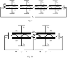
- a microwell electrode comprising: a substrate and an insulating layer on a surface of the substrate; one or more first electrodes; one or more second electrodes each arranged opposite to each first electrode, wherein a channel is defined by and located between each first electrode and the second electrode opposite thereto, and the channel has at least one end in communicaton with a chamber; and one or more guiding electrodes located in the chamber, wherein the first electrode, the second electrode and the guiding electrodes are located on a surface of the insulating layer away from the substrate.
- the guiding electrode can guide a charged substance into the channel and/or control the movement of a charged substance in the channel.
- the microwell electrode further comprises: a first supporting element for supporting the one or more first electrodes.
- a first supporting element for supporting the one or more first electrodes.
- each of the first electrodes is located on a sidewall of the first supporting element.
- the microwell electrode comprises a plurality of first electrodes and a plurality of first supporting elements, each of the first electrodes is supported by a corresponding first supporting element.
- the microwell electrode comprises a plurality of second electrodes, the microwell electrode further comprising: a plurality of second supporting elements, each of the second electrodes is supported by a corresponding second supporting element.
- each of the second electrodes is located on a sidewall of a second supporting element.
- the first electrode comprises a plurality of segment separated from each other.
- the second electrode comprises a plurality of segment separated from each other.
- the first electrode comprises a plurality of segments separated from each other, and the microwell electrode further comprises a plurality of first supporting elements, each segment of the first electrode is supported by a corresponding first supporting element.
- the second electrode comprises a plurality of segments separated from each other, and the microwell electrode further comprises a plurality of second supporting elements, each segment of the second electrode is supported by a corresponding second supporting element.
- the first supporting element is a conductive element.
- a voltage can be applied to the first electrode via the first supporting element.
- the first supporting element is a non-conductive element.
- the first supporting element is mainly used to support the first electrode, and preferably, a voltage can be applied to the first electrode via a wire embedded in the first supporting element.
- the second supporting element is a conductive element.
- a voltage can be applied to the second electrode via the second supporting element.
- the second supporting element is a non-conductive element.
- the second supporting element is mainly used to support the second electrode.
- a voltage can be applied to the second electrode via a wire embedded in the second supporting element.
- the microwell electrode may further comprise a nanostructure capable of immobilizing an enzyme or a chemical substance to be detected.
- the nanostructure is located on the bottom or a sidewall of the chamber, or on the bottom or a sidewall of the channel, or on the guiding electrodes.
- the nanostructure is formed by a material selected from a group consisting of a metal, a metal oxide, an inorganic polymer, an organic polymer, or any combination thereof.
- the channel has a width of 0.5-100nm, for example, 1nm, 2nm, 10nm, 50nm, 80nm, etc; and/or the channel has a length of 50nm-100 ⁇ m, for example,100nm, 500nm, 5 ⁇ m, 10 ⁇ m, 30 ⁇ m, etc; and/or the channel has a depth of 0-10 ⁇ m, for example, 100nm, 300nm, 1 ⁇ m, 2 ⁇ m, 8 ⁇ m, etc.
- the first electrode has a thickness of 1-1000nm, for example, 30nm, 50nm, 200nm, 600nm, 800nm, etc.
- the second electrode has a thickness of 1-1000nm, for example, 30nm, 50nm, 200nm, 600nm, 800nm, etc.
- the first electrode and the second electrode are formed by the same material.
- the first electrode and the second electrode are formed by different materials.
- the first supporting element, the first electrode and the second electrode may be formed by the same material, or by different materials.
- the first electrode is formed by a material selected from a group consisting of platinum, gold, indium tin oxide, carbon-based material(s), silicon or other conductive materials
- the second electrode is formed by a material selected from a group consisting of platinum, gold, indium tin oxide, carbon-based material(s), silicon or other conductive materials
- the guiding electrodes are formed by a material selected from a group consisting of silicon, platinum, gold, indium tin oxide, or carbon-based material(s).
- the conductive element is formed by a material selected from a group consisting of silicon, platinum, gold, silver, indium tin oxide, carbon-based material(s) or other conductive materials.
- the non-conductive element is formed by a material selected from a group consisting of silicon oxide, silicon nitride, silicon oxynitride, borophosphosilicate glass and the like.
- the first supporting element has a sectional shape of elliptical, circular, polygonal, or gear shape in a direction parallel to a surface of a substrate.
- the bottom surface of the chamber and the bottom surface of the channel are in the same plane or different planes.
- the microwell electrode further comprises: a substrate and an insulating layer on the substrate, where the first electrode, the second electrode and the guiding electrodes are located on the insulating layer.
- the guiding electrodes are substantially perpendicular to the first electrode or the second electrode. That is, the electric field direction between the guiding electrodes is substantially perpendicular to the electric field direction between the first electrode and the second electrode after applying voltages to the guiding electrodes, the first electrode and the second electrode.
- the microwell electrode further comprises: a passivation layer located on the surface(s) of the first electrode and/or the second electrode.
- microwell electrode array comprising: one or more microwell electrodes according to any one of the above embodiments.
- the microwell electrode array comprises a plurality of microwell electrodes.
- the number of the microwell electrodes may be 100, 10000, 10 6 or 10 8 , etc.
- the plurality of microwell electrodes in the microwell electrode array are arranged in an elliptical, a circular, an annular, a fan, a rectangular, a square, a zigzag, or a gear shape, or as a matrix of rows and columns, or as laminated layers, etc.
- more than one microwell electrodes are independent from each other, or connected in series, or connected in parallel.
- the plurality of microwell electrodes in the microwell electrode array share one guiding electrode.
- a sensor chip comprising: the microwell electrode array according to the above embodiment.
- the sensor chip and a corresponding integrated circuit can be manufactured in a process matched with the CMOS process.
- the number of microwell electrodes included in a microwell electrode array on a sensor chip can be determined according to the size of the microwell electrode, the properties of a molecule to be detected, cost or other factors.
- the microwell electrode array may be, as an example, a 10 ⁇ 10 array, 100 ⁇ 100 array, 1000 ⁇ 1000 array or 10 4 ⁇ 10 4 array, etc.
- a sequencing system comprising: the sensor chip according to the above embodiment.
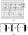
- a method for manufacturing a microwell electrode comprising: providing a substrate structure comprising a substrate with an insulating layer on its surface and a first supporting element material layer on the insulating layer, wherein the first supporting element material layer has successively on its sidewall a first electrode material layer, a sacrificial material layer, a second electrode material layer and a second supporting element material layer; patterning the first supporting element material layer, the first electrode material layer, the sacrificial material layer, the second electrode material layer and the second supporting element material layer to form one or more chambers, a first supporting element, and form a first electrode, a sacrificial layer, a second electrode and a second supporting element successively located on the sidewall of the first supporting element; forming one or more guiding electrodes in the chamber; removing the sacrificial layer on the sidewall of the first supporting element to form a channel between the first electrode and the second electrode, wherein the channel has at least one end in communication with the chamber.
- the step of providing the substrate structure comprises: providing a substrate with an insulating layer on its surface; forming a first supporting element material layer on a portion of the insulating layer; depositing a first electrode material layer to cover the upper surface and a sidewall of the first supporting element material layer; removing the first electrode material layer on the upper surface of the first supporting element material layer; depositing a sacrificial material layer to cover the upper surface of the first supporting element material layer, the upper surface and a sidewall of the remaining first electrode material layer; removing the sacrificial material layer on the upper surface of the first supporting element material layer and the upper surface of the remaining first electrode material layer; depositing a second electrode material layer to cover the upper surface of the first supporting element material layer, the upper surface of the remaining first electrode material layer and a upper surface and a sidewall of the remaining sacrificial material layer; removing the second electrode material layer on the upper surface of the first supporting element material layer, the upper surface of the remaining first electrode material layer, and the upper surface of the remaining sacri
- the guiding electrodes are substantially perpendicular to the first electrode; and/or the guiding electrodes are substantially perpendicular to the second electrode.
- the method before removing the sacrificial layer on the sidewall of the first supporting element, the method further comprises: forming a passivation layer on a surface of at least one of the first supporting element, the second supporting element, the first electrode, or the second electrode.
- the method before removing the sacrificial layer on the sidewall of the first supporting element, the method further comprises: removing a portion of the top of the first supporting element and a portion of the top of the second supporting element to expose a portion of the first electrode, a portion of the sacrificial layer and a portion of the second electrode; depositing a passivation layer on the remaining first supporting element, the remaining second supporting element, the exposed portion of the first electrode, the exposed portion of the sacrificial layer and the exposed portion of the second electrode; planarizing the deposited passivation layer to form a passivation layer on the remaining portion of the first supporting element and the remaining portion of the second supporting element, and expose the sacrificial layer.
- the step of patterning the first supporting element material layer, the first electrode material layer, the sacrificial material layer, the second electrode material layer and the second supporting element material layer comprises: separating the first electrode material layer and/or the second electrode material layer into a plurality of segments, so that the first electrode and/or the second electrode formed each comprises a plurality of segments separated from each other.
- the method further comprises: forming a nanostructure capable of immobilizing an enzyme or a chemical substance to be detected on the bottom or a sidewall of the chamber, or on the bottom or a sidewall of the channel, or on the guiding electrodes.
- the nanostructure is formed by a material selected from a group consisting of a metal, a metal oxide, an inorganic polymer, an organic polymer, or any combination thereof.
- the channel has a width of 0.5-100nm, for example, 1nm, 2nm, 10nm, 50nm, 80nm, etc; and/or the channel has a length of 50nm-100 ⁇ m, for example,100nm, 500nm, 5 ⁇ m, 10 ⁇ m, 30 ⁇ m, etc; and/or the channel has a depth of 0-10 ⁇ m, for example, 100nm, 300nm, 1 ⁇ m, 2 ⁇ m, 8 ⁇ m, etc.
- the first electrode has a thickness of 1-1000nm, for example, 30nm, 50nm, 200nm, 600nm, 800nm, etc.
- the first electrode and the second electrode are formed by the same material.
- the first electrode and the second electrode are formed by different materials.
- the first electrode is formed by a material selected from a group consisting of silicon, platinum, gold, indium tin oxide, or carbon-based material(s); and/or the sacrificial layer is formed by a material selected from a group consisting of chromium, tungsten, aluminum, aluminum oxide, silicon, silicon oxide, silicon nitride; and/or the second electrode is formed by a material selected from a group consisting of silicon, platinum, gold, silver, indium tin oxide, or carbon-based material(s); and/or the guiding electrodes are formed by a material selected from a group consisting of silicon, platinum, gold, silver, indium tin oxide, or carbon-based material(s).
- the first supporting element and the second supporting element comprise conductive elements.
- the conductive element is formed by a material selected from a group consisting of silicon, platinum, gold, silver, indium tin oxide, or carbon-based material(s).
- the first supporting element and/or the second supporting element have a sectional shape of elliptical, circular, rectangular, square, or gear shape in a direction parallel to a surface of the substrate.
- the invention also provides a method for analysis of a chemical substance, comprising the steps of:
- the type of the charged molecule is identified with the first electrode, the second electrode and/or the guiding electrode based on one or more effects selected from a group consisting of oxidation-reduction effect, electric resistance effect, capacitance effect, field effect, and tunneling effect.
- the chemical substance to be tested is selected from a group consisting of a biological molecule (such as a nucleic acid, protein, lipid, and polysaccharide), a compound, an organic polymer, etc.
- a biological molecule such as a nucleic acid, protein, lipid, and polysaccharide
- the chemical substance to be tested is a nucleic acid, such as DNA or RNA.
- the chemical substance to be tested comprises or consists of one or more basic units (such as nucleotides, amino acids, and polymeric monomers).
- the basic unit of the chemical substance to be tested is unmodified.
- the basic unit of the chemical substance to be tested is modified by a label molecule.
- the reaction solution contains a free basic unit modified by a label molecule, which release a free label molecule after the reaction.
- the free label molecule is charged (i.e., a charged molecule), and can enter the channel under the action of the guiding electrode, or be accumulated in the channel under the action of the guiding electrode. Therefore, the type of the charged molecule can be identified by using the first electrode, the second electrode and/or the guiding electrode, and therefore the information of the chemical substance to be tested is obtained.
- the reaction solution contains one or more types of free, label molecule-modified basic units. In an embodiment, the reaction solution contains at least two types (such as three, four, or more types) of free, label molecule-modified basic units. In an embodiment, different basic units are modified by the same label molecule. In another embodiment, different basic units are modified by different label molecules.
- the free label molecule is a redox active substance
- the first electrode and the second electrode are used as detection electrodes, to identify the type of the label molecule by an oxidation-reduction effect.
- the type of the charged molecule in addition to the oxidation-reduction effect, in the step (4), can be identified with the first electrode, the second electrode and/or the guiding electrode based on one or more electric resistance effect, capacitance effect, field effect, and tunneling effect.
- the charged molecule can be detected by using one or more detection principles, so as to improve the accuracy of the detection result. For example, when an electric field is generated between guiding electrodes, any molecule in a channel will physically block ion current, thereby resulting in a detectable reduction in ion current.
- the accuracy of the detection of the charged molecule can be further improved by selecting a label molecule of a suitable size and a channel of a suitable length, and by the signal characteristic resulted from the electric resistance effect. Therefore, a person skilled in the art can select a combination of methods for identification of the types of the charged molecule depending on practical need. For example, a combination of field effect and oxidation-reduction effect, a combination of capacitance effect and oxidation-reduction effect, a combination of electric resistance effect and oxidation-reduction effect, or a combination of oxidation-reduction effect, electric resistance effect and field effect, can be used to identify the types of the charged molecule.
- the first electrode and the second electrode are used as a source electrode and a drain electrode, respectively, and the modification film is used as a conducting channel between the two electrodes.
- a recognition site for a label molecule can be formed on the conducting channel and used as a gate electrode, so as to form a field-effect transistor.
- the first electrode and/or the second electrode each can be separated into a plurality of segments, i.e., two or more segments (e.g., 3-4 segments).
- each segment of electrode has a different voltage.
- the voltage of each segment of electrode corresponds to the response voltage (redox potential window) of a label molecule. Therefore, for a label molecule, only the segment of electrode, the voltage of which corresponds to the response voltage of the label molecule, can respond to the label molecule and generate a signal; while the other segments of electrode can neither respond to the label molecule nor generate a signal.
- the first electrode and/or the second electrode is separated into a plurality of segments, such as 2-4 segments of transverse electrodes, and each single segment of electrode can be controlled independently so as to generate a different voltage.
- each microwell electrode may have a plurality of channels.
- a plurality of channels provided in a microwell electrode can greatly increase surface area for detection, and therefore can not only improve signal strength, but also reduce potential contamination effect.
- the combination of a microwell electrode array and a chamber also provides more controllable modes for sample injection.
- the channel may be open-ended.
- the process for manufacturing an open-ended channel is more simple and easier, and the open-ended channel is convenient for the injection of a sample and a liquid, and can better achieve a balance between speed and accuracy.
- the channel may be close-ended.
- the close-ended channel is favorable for controlling and reducing the interference of external impurity signal.
- the structure of the channels can be selected depending on particular conditions.
- the microwell electrode comprises open-ended channel(s), or close-ended channel(s), or both of open-ended channel(s) and close-ended channel(s).
- the chemical substance to be tested is a nucleic acid molecule, and in the step (2), the reaction solution is subjected to polymerization of nucleotides.
- the method is used for analysis of the composition, sequence, electric charge, size or concentration of a chemical substance.
- the invention also provides a method for analysis of a nucleic acid molecule, comprising the steps of:
- the type of the free label molecule is identified by one or more of oxidation-reduction effect, electric resistance effect, capacitance effect, field effect, and tunneling effect.
- the type of the label molecule is identified by oxidation-reduction effect.
- the free label molecule may be a redox active substance that is reactive in a circular redox reaction, or may be converted to a redox active substance that is reactive in a circular redox reaction.
- the free label molecule may be physically or chemically converted to a redox active substance that is reactive in a circular redox reaction.
- the redox active substance can be subjected to a circular redox reaction between the first electrode and the second electrode, resulting in a detectable current.
- the type of the label molecule can be identified by the detectable current.
- the type of the label molecule in addition to the above-mentioned oxidization-reduction effect, the type of the label molecule can be identified by one or more of electric resistance effect, capacitance effect, field effect, and tunneling effect.
- the entrance of the free label molecule is led and/or controlled by using the guiding electrode or other means, and potentials are applied to the first electrode and the second electrode of the channel, respectively.
- the label molecule can be subjected to a circular redox reaction between the first electrode and the second electrode, and a detectable redox current pulse signal is generated.
- the detectable redox current pulse signal By using the detectable redox current pulse signal, the label molecule can be specifically identified and detected. When a matching potential is provided between the first electrode and the second electrode but no pulse signal is detected, it indicates that the label molecule is not present.
- each of the at least one dNTP or NTP molecule or analogue carries a label molecule having a different redox potential window.
- the type of the label molecule in the channel can be identified by changing the potential of the first electrode and/or the second electrode, and determining whether a redox current pulse signal is generated under various potential conditions, and optionally, determining the information such as the signal amplitude of the pulse signal.
- each of the at least one dNTP or NTP molecule or analogue carries a label molecule having a different redox potential window.
- the first electrode and/or the second electrode in the channel is separated into a plurality of segments, and each segment is applied with a potential corresponding to the redox potential window of a different label molecule. Therefore, when a label molecule passes the channel, a redox current pulse signal can only be detected in the electrode segment with a potential corresponding to the redox potential window of the label molecule, thereby identifying the type of the label molecule in the channel.
- reaction solution further comprises a phosphatase.
- the free label molecule is dephosphorylated in the presence of a phosphatase.
- the label molecule-modified dNTP, NTP or analogue is neutral in net charge or is negatively charged.
- the free label molecule is positively charged or negatively charged.
- the label molecule-modified dNTP, NTP or analogue is neutral in net charge or is negatively charged, and the free label molecule is positively charged.
- the positively charged free label molecule can migrate along the channel under the action of an electric field, while the label molecule-modified dNTP, NTP or analogue will not migrate in the chamber or channel as they are neutral or negatively charged.
- the label molecule-modified dNTP, NTP or analogue is negatively charged, and the free label molecule is negatively charged.
- the free label molecule, the label molecule-modified dNTP, NTP or analogue, and the unmodified dNTP, NTP molecule, all of which are negatively charged can migrate together along the channel under the action of an electric field.
- only the free label molecule is redox active, while the label molecule-modified dNTP, NTP molecule and the unmodified dNTP, NTP molecule are not redox active.
- the redox current signal can only be resulted from the free label molecule.
- the label molecule is linked to the phosphate group, base or saccharide group of the dNTP or NTP molecule or analogue.
- the label molecule is selected from one or more of: amino acids, peptides, carbohydrates, metal compounds, dyes, chemiluminescent compounds, nucleotides, aliphatic acids, aromatic acids, alcohol, aminophenyl, hydroxyphenyl, naphthyl, thiol group, cyano, nitro, alkyl, alkenyl, alkynyl, azido, or a derivative thereof.
- the label molecule is selected from one or more of: aminophenyl, hydroxyphenyl, naphthyl, variable-valency metal compounds (such as ferrocene, hexacyanoferrate, and ferrocyanide), anthraquinone, and methylene blue, and a derivative thereof.
- the label molecule is linked to the ⁇ -phosphate group of the dNTP or NTP molecule or analogue, and preferably, the label molecule is selected from a group consisting of aminophenyl, hydroxyphenyl, naphthyl, and a derivative thereof.
- the label molecule is linked to the base or saccharide group of the dNTP or NTP molecule or analogue; and preferably, the label molecule is selected from a group consisting of variable-valency metal compounds (such as ferrocene, hexacyanoferrate, and ferrocyanide), anthraquinone, and methylene blue, and a derivative thereof.
- variable-valency metal compounds such as ferrocene, hexacyanoferrate, and ferrocyanide
- each type of dNTP e.g., dATP, dTTP, dCTP, dGTP, dUTP
- NTP e.g., ATP, TTP, CTP, GTP, UTP
- step (3) all the four types of dNTP (for example, selected from a group consisting of dATP, dTTP/dUTP, dCTP, dGTP) or NTP (e.g., ATP, TTP, CTP, GTP, UTP) molecules are added simultaneously.
- the washing step following the incorporation of each base may be omitted, thereby greatly reducing the cost of reagents and accelerating the detection speed.
- the charge carried by the free label molecule can be adjusted by selecting a label molecule, so as to adjust the migration speed of the free label molecule under the action of a guiding electrode.
- the polymerase in the step (1), is immobilized on an insulated layer on the bottom of the chamber or channel, or immobilized on a guiding electrode.
- the polymerase is immobilized at a place close to the inlet port of the channel at the bottom of the chamber; preferably, the inlet port of the channel may be designed in a variety of shapes (such as a funnel shape), to hold a polymerase.
- a polymerase is immobilized in each chamber or channel.
- the nucleic acid molecule to be tested in the reaction solution is a single-stranded nucleic acid molecule.
- each polymerase can capture a single-stranded nucleic acid molecule or a complex formed from the hybridization of a nucleic acid molecule and a primer.
- the insulated layer is formed by a material selected from a group consisting of silicon dioxide, silicon oxynitride, silicon nitride or other insulating materials (e.g., Carbon Doped Oxide (CDO), silicon carbide, organic polymer such as polyimide, octafluorocyclobutane or polytetrafluoroethylene, fluorosilicate glass (FSG), and organic silicate such as silsesquioxane, siloxane or organic silicate glass).
- CDO Carbon Doped Oxide
- silicon carbide organic polymer such as polyimide, octafluorocyclobutane or polytetrafluoroethylene, fluorosilicate glass (FSG), and organic silicate such as silsesquioxane, siloxane or organic silicate glass.
- FSG fluorosilicate glass
- organic silicate such as silsesquioxane, siloxane or organic silicate glass
- a functionalizable region and/or a molecule-binding region may be further provided between the insulated layer and the polymerase.
- the functionalizable region comprises a functionalizable material such as silicon dioxide, hafnium oxide, aluminum oxide, tantalum oxide, and/or zirconium oxide.
- the functionalizable material may be functionalized with a linking molecule selected from a group consisting of: silicane (e.g., aminopropyltriethoxysilane), thiol (-SH), disulfide (-S-S-), isothiocyanate, alkene and alkyne.
- the molecule-binding region comprises a probe molecule.
- the probe molecule is, for example, selected from a group consisting of a biotin, an avidin, an antibody, an antigen, a receptor, a ligand, a DNA sequence, a RNA sequence, a protein and a ligand thereof.
- a binding molecule can be selected so that the polymerase is immobilized in a suitable direction.
- the method is used for analysis of the sequence, composition, electric charge, size or concentration of a nucleic acid molecule.
- an electrolytic solution and a reaction solution may be added to the surface of the microwell electrode so that all the chambers and channels are filled with the electrolytic solution and the reaction solution.
- their potentials can be set independently so as to control or detect reactive molecules independently.
- the guiding electrode controls the entrance of an electrolytic solution and a redox active substance into a channel, and the first electrode and the second electrode are used as a redox reaction detection device for detecting the redox active substance.
- the electric field formed by the guiding electrode is favorable for entrance of charged molecules (such as positively charged molecules) into a channel, and accumulation thereof in the channel, so as to reduce the possibility that the molecules diffuse out from the channel, which in turn can enhance the strength of the signal detected.
- charged molecules such as positively charged molecules
- the voltage of the guiding electrode can be adjusted so as to control the transport speed of the charged molecules.
- the polymerase may also be modified so that the optimal synthesis speed matches the transport speed of the molecules.
- micro or nano-scale fluid mechanics may also be used to control the migration of molecules in a channel.
- the nucleic acid molecule includes deoxyribonucleic acid (DNA), ribonucleic acid (RNA), and polymers of other analogues linked together via phosphodiester bond.
- Polynucleotide may be a fragment of a genome, a gene or a part thereof, cDNA or a synthesized deoxyribonucleic acid sequence.
- Nucleotides included in a polynucleotide may be naturally occurring deoxyribonucleotides such as adenine, cytosine, guanine or thymine linked to 2'-deoxyribose, or ribonucleotides such as adenine, cytosine, guanine or uracil linked to ribose.
- a polynucleotide or oligonucleotide (such as a probe or primer) may further comprise a nucleotide analogue, including a non-naturally occurring synthetic nucleotide or a modified naturally occurring nucleotide.
- the redox cycle refers to an electrochemical method in which a molecule that can be reversely oxidized and/or reduced (i.e., a redox active molecule) migrates between at least two independently biased electrodes, wherein one of the at least two electrodes has a potential lower than the reduction potential of the redox active molecule to be detected, while the other of the at least two electrodes has a potential higher than the oxidation potential of the redox active molecule, so that electrons shuttle between the independently biased electrodes (i.e., the molecule is oxidized at the first electrode, and then diffuses to the second electrode and reduced there, or vice versa, the molecule is reduced and then oxidized, depending on the molecule and the potential of the electrode when biased).
- a molecule that can be reversely oxidized and/or reduced i.e., a redox active molecule
- a guiding electrode can be provided to prevent the diffusion of a redox active substance outside the channel, so as to increase the effective concentration of the redox active substance in the channel.
- the redox active substance (or the redox active molecule) has the general meanings in the art, and is a molecule that can be reversely oxidized and/or reduced for many times.
- the phosphatase is, for example, selected from a group consisting of alkaline phosphatase, acid phosphatase, protein phosphatase, polyphosphatase, sugar-phosphatase and pyrophosphatase.
- the incorporation of the label molecule-modified dNTP, NTP or analogue releases the label molecule-pyrophosphate (PPi) into the solution.
- the phosphatase functions to remove pyrophosphate from the label molecule-pyrophosphate.
- the removal of the phosphate group further activates the redox active substance, and therefore the presence of the redox active substance can be detected by a electrochemical mean.
- the silane molecule can have the chemical formulae X 3 -Si-YR", X2-Si-(N)YR” or X-Si-(N 2 )YR", wherein X is a leaving group, such as -Cl, -OCH 3 or -OCH 2 CH 3 , R" is a reactive coupling group, such as -NH 2 , -COOH, -COH, -CHCH 2 or -SH, and Y is a non-reactive group, such as an alkyl group.
- the organic group for use in coupling, as presented by the silane molecule attached on a surface may be, for example, carboxyl group, aldehyde, ester, alkene, alkyne, thiol, isothiocyanate, isocyanate, substituted amine, epoxide, small molecule such as biotin, or ethanol.
- Y is a non-reactive group, such as, a hydrocarbon compound having 1 to 16 carbon atoms. Examples of -YR" include -(CH 2 ) 3 NH 2 , -(CH 2 ) 2 COOH and -(CH 2 ) 2 SH.
- silanes include (3-aminopropyl)triethoxysilane (APTS), mercaptosilane and glycidoxy trimethoxy silane (having the coupling group of an epoxide).
- APTS (3-aminopropyl)triethoxysilane
- mercaptosilane mercaptosilane
- glycidoxy trimethoxy silane having the coupling group of an epoxide.
- the surface to be silylated may react with, for example, silane molecules in solution, or silane molecules as silane gas.
- the base for example, is selected from a group consisting of adenine, guanine, cytosine, thymine, uracil, 7-deazaguanine, 7-deazaadenine, and 5-methylcytosine.
- the primer (primer sequence) is a short oligonucleotide of a suitable length (for example, about 18-24 bases in length) that is generally synthesized chemically, and is sufficient to be hybridized to a target nucleic acid (for example, a single-stranded DNA) and allow addition of nucleotide residues thereto or synthesis of an oligonucleotide or a polynucleotide therefrom under suitable conditions as well known in the art.
- the primer is a DNA primer, i.e., a primer consisting or mainly consisting of deoxyribonucleotide residues.
- the primer is designed to having a reverse complementary sequence of a region of a template/target nucleic acid (such as a single-stranded DNA) which is hybridizable to the primer. Nucleotide residues are added to the 3' end of a primer by formation of a phosphodiester bond so as to produce an extension product; or nucleotide residues are added to the 3' end of the extension product by formation of a phosphodiester bond so as to produce another extension product.
- a template/target nucleic acid such as a single-stranded DNA
- incorporation of the dNTP, NTP or analogue into an oligonucleotide or a polynucleotide refers to the formation of a phosphodiester bond between the 3' carbon atom of the nucleotide residue at the 3' end of the polynucleotide and the 5' carbon atom of the dNTP, NTP or analogue.
- the polymerase includes DNA polymerase, RNA polymerase, reverse transciptase, and the like, the functions or kinds of which are well known in the art.
- the DNA polymerase may, for example, have 3' to 5' exonuclease activity or not, including for example, E. coli DNA polymerase, Klenow fragment, Phusion DNA polymerase, 9°N DNA polymerase, KOD polymerase, Therminator DNA polymerase, Taq DNA polymerase, Vent DNA polymerase, and the like.
- an ideal base incorporation rate (e.g., 1-100 bases per second) is achieved in real-time sequencing.
- a polymerase is specifically modified to be more suitable for application.
- a polymerase which can be used to synthesize a polymer quickly, continuously and accurately, is selected or obtained from a clone bank of DNA polymerases, with a proviso that a single DNA polymerase molecule can achieve synthesis of 1-100 kb DNA without dissociation from the template strand.
- the polymerase lacks exonuclease activity, and the error rate of base incorporation shall be as low as 10 -5 -10 -6 /incorporated base.
- the bias of the polymerase for each specific nucleotide can greatly enhance the sequencing specificity.
- a polymerase having different detectable bias for DNA, RNA and methylated base is favorable for sequencing.
- other properties may include thermal stability, stable buffer system, working capability under accumulation of macromolecules, and tolerance to a lot of side products (pyrophosphate).
- suitable mutants which have a polymerization rate matching the ability of the detection device, are screened from a clone bank of polymerases, so that the true base incorporation and the non-incorporation can be distinguished from each other to the largest extent.
- the polymerase is also required to enable incorporation of modified nucleotides. Therefore, it needs to select polymerase mutants and modified nucleotides, which match the ability of the detection device.
- a buffer may also be used to change the base incorporation rate (for example, the incorporation rate of a specific nucleotide may be decreased or increased by virtue of pH and ions).
- a polymerase mutant By determining the detention time of nucleotides in a polymerase pocket, a polymerase mutant can be selected for its higher or lower bias for a specific nucleotide. By enzyme kinetic measurement, it can reduce the probability of false positive incorporation, and can distinguish a true incorporation signal from a device noise.
- the residues in a candidate can be found, thereby promoting discovery of a new specific and stable interaction.
- Another characteristic of the enzyme is that it can release the nucleic acid molecule at the end point, so as to enable the entrance of a new primer-carrying template DNA and the sequencing to begin.
- a 1-10-100-1000 kb template can be sequenced in a channel.
- a microwell electrode of the present invention has the following advantages: being able to comprise a plurality of nanochannels in a microwell electrode , thus reducing the influence of contamination of electrode surface; being able to guide the flow of a reagent by an electric field and electroosmotic flow generated by a guiding electrode in a nano-channel; being easy to integrate with a microfluid to achieve the purpose of reagent interaction; being easy for large-scale manufacturing of electrode arrays; being compatible with a variety of signal detection mechanisms, including electronic signal detection (e.g., based on a redox cycle, FET (field effect transistor), electrochemical, electrical impedance); making physical amplification of a signal possible; allowing the integration with a monolithic CMOS; being able to control the movement of a nucleic acid molecule by an electric field; enabling single molecule detection of a chemical substance to be detected by detecting an electrical signal of a label molecule; greatly increasing read length; and being sensitive for detection signal.
- electronic signal detection e
- Method for analysis of a chemical substance of the present invention can be used in molecular detection and analysis, molecular diagnosis, disease detection, substance identification, and DNA detection and sequencing, etc.
- Fig. 1A is a top view of a microwell electrode according to an embodiment of the present invention.
- Fig. 1B is a sectional view taken along B-B' shown in Fig. 1A .
- Fig. 1C is a sectional view taken along C-C' shown in Fig. 1A .
- a microwell electrode 100 may comprise one or more first electrode(s) 301. Different first electrodes 301 can be separated from each other, for example, different first electrodes 301 may have gaps therebetween or the gaps may be filled with an insulating layer. Exemplarily, the first electrode 301 may have a thickness d1 of about 1-1000nm, for example, 30nm, 50nm, 200nm, 600nm, 800nm or the like.
- the first electrode 301 may be formed by a material selected from a group consisting of platinum, gold, silver, indium tin oxide, carbon-based materials (for example, diamond, graphite, amorphous carbon, carbon nanotubes, etc), silicon or any combination thereof.
- the microwell electrode 100 further comprises one or more second electrodes 303 each arranged opposite to one first electrode 301.
- a channel 601 is provided between each first electrode 301 and its opposite second electrode 303.
- the channel 601 has at least one end in communication with a chamber 401.
- the second electrode 303 may have a thickness d2 of about 1-1000nm, for example, 30nm, 50nm, 200nm, 600nm, 800nm or the like.
- the second electrode 303 may be formed by a material selected from a group consisting of platinum, gold, silver, indium tin oxide, carbon-based materials (for example, diamond, graphite, amorphous carbon, carbon nanotubes, etc), silicon or any combination thereof.
- the bottom surface of the chamber 401 and the bottom surface of the channel 601 may be in the same plane. In another embodiment, the bottom surface of the chamber 401 and the bottom surface of the channel 601 may be in different planes.
- the microwell electrode 100 further comprises one or more guiding electrodes 501 located in the chamber 401.
- the guiding electrode 501 may lead a charged substance into the channel 601. Further, the guiding electrode 501 may also control the movement of a charged substance in the channel 601.
- a leading electric field produced between the guiding electrodes 501 can control thea charged substance (for example, a redox-active molecule) to enter into the channel 601, and control the movement of a charged substance (for example, a redox-active molecule) in the channel 601 so that the charged substance cannot easily move outside the channel 601.
- this guiding electrode 501 can be used to control the movement of a charged substance in one or more channels 601 that communicate with the chamber 401. If a plurality of guiding electrodes 501 are provided in the chamber 401, each of the guiding electrodes 501 can control the movement of a charged substance in an adjacent channel 601 thereto, respectively.
- the guiding electrode 501 may be formed by a material selected from a group consisting of silicon, platinum, gold, ITO, carbon-based materials or any combination thereof.
- the guiding electrode 501 can be substantially perpendicular to the first electrode 301 or the second electrode 303 (as shown in Fig. 1 ).
- the guiding electrode 501 is not necessarily perpendicular to the first electrode 301 or the second electrode 303, and an angle of other degree therebetween is also possible.
- a microwell electrode provided in the present invention can be used in, but not limited to, nucleic acid sequencing, in which case, the chamber 401 may be a microfluidic chamber.
- the manufacturing process of a microwell electrode can be compatible with CMOS process, and is easy to mass manufacture. Further, a plurality of signaling mechanisms can be adopted in nucleic acid sequencing and a longer read length can be achieved. Further, since a microwell electrode may comprise multiple channels at the same time, the effect of electrode contamination on sequencing results can be reduced, thus making sequencing results more accurate.
- Fig. 2A is a schematic diagram showing working principle of a microwell electrode according to an embodiment of the present invention.
- the microwell electrode comprises a set of detection electrodes (a first electrode 301 and a second electrode 303) and a set of guiding electrodes 501.
- a voltage V 1 is applied on the first electrode 301
- a voltage V 2 is applied on the second electrode 303
- a voltage difference V g is produced between the two guiding electrodes 501.
- a leading electric field between the two guiding electrodes 501 can pull a molecule to be detected (for example, a redox-active label molecule) into a channel between the two detection electrodes.
- the label molecule undergoes a redox cycle reaction between the two detection electrodes.
- the redox cycle reaction produces a corresponding current signal, which can be detected by the two detection electrodes.
- Different label molecules correspond to different current signals; therefore, the type of a label molecule can be determined according to the detected current signal.
- Fig. 2B is a schematic diagram showing the corresponding relationship between different bases and detection voltages applied on a first electrode and a second electrode.
- a current signal caused by the molecule to be detected can be detected.
- the voltages V 1 and V 2 can be put in a redox potential window corresponding to a molecule to be detected by changing the values of the voltages V 1 and V 2 several times in a time period to, and then the type of the molecule to be detected can be identified. In this way, current signals of different molecules to be detected can be detected at different voltages V 1 and V 2 . As shown in Fig.
- bases A, T, C, and G correspond to different voltages V 1 and V 2 , respectively.
- base A corresponds to voltages V 1A and V 2A
- base T corresponds to voltages V 1T and V 2T
- base C corresponds to voltages V 1C and V 2C
- base G corresponds to voltages V 1G and V 2G .
- the voltages V 1 and V 2 can be put in the redox potential windows of the label molecules corresponding to bases T, C or G, the type of a label molecule can be identified, and then the type of the base corresponding to the label molecule can be identified.
- the microwell electrode may further comprise a substrate 101 and an insulating layer 102 on the substrate 101.
- the first electrode 301, the second electrode 303 and the guiding electrodes 501 can be disposed on the insulating layer 102.
- the substrate 101 may be, for example, a silicon substrate, a substrate made of a Group III-V semiconductor material, a silicon on insulator (SOI) substrate, or may be an oxide semiconductor (such as ZnO, CdO, TiO 2 , Al 2 O 3 , or SnO) substrate, or may be a substrate made of an insulating material, such as a quartz glass, or a soda glass.
- the insulating layer 102 may be typically a silicon oxide (e.g., silicon dioxide), a silicon nitride (e.g., SiN), a silicon nitrogen oxide, etc.
- the microwell electrode may further comprise a first supporting element 201 for supporting the first electrode 301.
- the microwell electrode may comprise a plurality of first electrodes 301, all of which can be supported by the first supporting element 201.
- the microwell electrode may comprise a plurality of first electrodes 301 and a plurality of first supporting elements 201, and each of the first electrodes 301 can be supported by a corresponding first supporting element 201, respectively.
- the microwell electrode may comprise a plurality of second electrodes 303 and a plurality of second supporting elements 304, and each of the second electrodes 303 can be supported by a corresponding second supporting element 304, respectively.
- the above first supporting element 201 and second supporting element 304 may be conductive elements or non-conductive elements, and preferably, conductive elements.
- the first supporting element 201 and the second supporting element 304 mainly serve to support the first electrode 301 and the second electrode 303.
- voltages can be applied to the first electrode 301 and the second electrode 303 through applying voltages to the first supporting element 201 and the second supporting element 304.
- the above conductive elements may be formed by a material selected from a group consisting of silicon (for example, polysilicon), platinum, gold, silver, indium tin oxide, or carbon-based material(s), etc.
- the above non-conductive elements may be formed by a material selected from silicon oxide, silicon nitride, silicon oxynitride, borophosphosilicate glass, and the like.
- the first supporting element 201 may have a sectional shape of an elliptical, circular, polygonal, square or gear shape in the direction parallel to the surface of the substrate 101. It should be understood that the present invention is not limited to the above exemplary shapes.
- the material of the above first electrode 301 and the material of the second electrode 303 may be the same or may be different.
- one of the first electrode 301 and the second electrode 303 may be made of an electrode material which is easy to be oxidized, and the other may be made of an electrode material liable to be reduced.
- the microwell electrode 100 may further comprise a passivation layer 701 formed on the surface of at least one of the first electrode 301, the second electrode 303, the first supporting element 201 (if any), the second supporting element 304 (if any).
- the passivation layer 701 may be a silicon nitride (e.g., SiN), a silicon oxide (e.g., SiO 2 ) and the like. The passivation layer 701 may serve to protect the microwell electrode.
- the passivation layer 701 when performing nucleic acid sequencing by the microwell electrode, only a region that is not covered by the passivation layer 701 can contact reaction solution, so that damages to certain components of the microwell electrode can be avoided.
- the passivation layer 701 may also reduce noises produced in the sequencing process.
- the microwell electrode 100 may further comprise a nanostructure 801 (e.g., a nanodot) capable of immobilizing an enzyme or a chemical substance 802 to be detected.
- the nanostructure 801 can be located on the bottom or a sidewall of the chamber 401 (as shown in Figs. 1A and 1B ), or on the bottom or a sidewall of the channel 601 (not shown), or on the guiding electrode 211.
- the size of the nanostructure 801 may be 1-100nm, for example, 8nm, 20nm, 60nm and the like.
- the nanostructure 801 may be formed by a metal oxide; preferably, the metal oxide is a transition metal oxide such as zirconium dioxide (ZrO 2 ) or hafnium dioxide (HfO 2 ).
- the nanostructure 801 may also be formed by a metal; preferably, the metal is an inert metal such as gold or platinum.
- the nanostructure 801 may also be formed by a material selected from an inorganic polymer, an organic polymer, or any combination thereof.
- the first electrode 301 and/or the second electrode 303 may comprise a plurality of segments separated from each other, for example, two or more segments. A description will be given below with reference to different implementations.
- the first electrode 301 comprises a plurality of segments separated from each other, and the second electrode 303 comprises only one segment.
- the microwell electrode may comprise a plurality of first supporting elements 201, each segment of the first electrode 301 can be supported by a corresponding first supporting element 201.
- a voltage can be applied to the second electrode 303 and voltages corresponding to different molecules (for example, redox label molecules) to be detected can be applied to the various segments of the first electrode 301.
- time information that the molecule to be detected moves from one segment of the first electrode 301 to another, in addition to current signal information of the molecule to be detected, can be also obtained, which is helpful to improve the detection resolution of different molecules to be detected.
- the first electrode 301 comprises a plurality of segments separated from each other
- the second electrode 303 also comprises a plurality of segments separated from each other, each segment of the first electrode 301 is arranged opposite to one segment of the second electrode 303.
- Each segment of the first electrode 301 can be supported by a corresponding first supporting element 201
- each segment of the second electrode 303 can be supported by a corresponding second supporting element 304.
- different voltages can be applied to each segment of the first electrode 301 and the segment of the second electrode 303 arranged opposite to this segment of the first electrode 301, when a molecule to be detected passes through various electrode segments sequentially under the control of a guiding electric field, only the electrode segments applied with a voltage therebetween corresponding to a redox potential window of the molecule can detect a current signal.
- different molecules to be detected can be detected by different segments of the first electrode 301 and the corresponding segments of the second electrode 303.
- the first electrode 301 may comprise one segment
- the second electrode 303 may comprise a plurality of segments separated from each other.
- a voltage can be applied to the first electrode 301, and voltages corresponding to the redox windows of different molecules to be detected (for example, redox label molecules) can be applied to the various segments of the second electrode 303.
- time information that the molecule to be detected move from one segment of the second electrode 303 to another, in addition to current signal information of the molecule to be detected can be also obtained, which is helpful to improve the detection resolution of different molecules to be detected.
- Fig. 3 is a schematic diagram showing a microwell electrode according to an embodiment of the present invention, wherein the first electrode and the second electrode each includes four segments.
- the first electrode 301 comprises a first segment 311 of the first electrode, a second segment 321 of the first electrode, a third segment 331 of the first electrode and a fourth segment 341 of the first electrode. Voltages applied to the first segment 311 of the first electrode to the fourth segment 341 of the first electrode are V 11 , V 21 , V 31 , and V 41 , respectively.
- the second electrode 303 comprises a first segment 313 of the second electrode, a second segment 323 of the second electrode, a third segment 333 of the second electrode and a fourth segment 343 of the second electrode.
- Voltages applied to the first segment 313 of the second electrode to the fourth segment 343 of the second electrode are V 12 , V 22 , V 32 , and V 42 , respectively.
- Each segment of the first electrode 301 is arranged opposite to one segment of the second electrode 303, and each segment of the first electrode 301 and the segment of the second electrode 303 arranged opposite thereto are used as a set of detection electrodes.
- the first segment 311 of the first electrode is arranged opposite to the first segment 313 of the second electrode, and these two segments are used as a set of detection electrodes.
- a detection voltage applied on each set of detection electrodes corresponds to a label molecule to be detected.
- a voltage difference between the two guiding electrodes 501 is V g .
- a label molecule to be detected passes through the four sets of detection electrodes sequentially under the control of the guiding electric field of guiding electrodes 501, only a set of detection electrodes that is applied with a detection voltage corresponding to the redox window of the label molecule to be detected can detect a current signal.
- the type of a label molecule to be detected can be determined according to the detection electrode that detects a current signal. For example, a detection voltage applied on the first set of detection electrodes corresponds to a redox window of a certain label molecule to be detected, upon detecting a current signal by the first set of detection electrodes, it can be determined that the label molecule to be detected has been detected.
- the present invention further provides a microwell electrode array, comprising one or more microwell electrodes according to any one of the above embodiments.
- a plurality of microwell electrodes may share a guiding electrode.
- Fig. 4A is a schematic diagram showing a microwell electrode array consisting of two microwell electrodes.
- the microwell electrode comprises a first microwell electrode and a second microwell electrode, the first microwell electrode and the second microwell electrode sharing an intermediate guiding electrode 501.
- the voltages applied on the first electrode 301 and the second electrode 303 of the first microwell electrode are V 11 and V 12 , respectively; and the voltages applied on the first electrode 301 and the second electrode 303 of the second microwell electrode are V 21 and V 22 , respectively.
- a voltage difference V g1 is applied on the two guiding electrodes 501 of the first microwell electrode, and a voltage difference V g2 is applied on the two guiding electrodes 501 of the second microwell electrode.
- a negatively charged label molecule is drawn into the channel of the first microwell electrode, and a positively charged label molecule is drawn into the channel of the second microwell electrode, thus achieving screening of label molecules.
- a microwell electrode array consisting of two microwell electrodes can recognize the charge polarity of a label molecule and can determine the type of the label molecule according to its current signal.
- Fig. 4B is a schematic diagram showing a microwell electrode array consisting of four microwell electrodes. As shown in Fig. 4B , the microwell electrode comprises a first microwell electrode, a second microwell electrode, a third microwell electrode and a fourth microwell electrode. These four microwell electrodes share an intermediate guiding electrode 501.
- the voltages applied on the first electrode 301 and the second electrode 303 of the first microwell electrode are V 11 and V 12 , respectively; the voltages applied on the first electrode 301 and the second electrode 303 of the second microwell electrode are V 21 and V 22 , respectively; the voltages applied on the first electrode 301 and the second electrode 303 of the third microwell electrode are V 31 and V 32 , respectively; and the voltages applied on the first electrode 301 and the second electrode 303 of the fourth microwell electrode are V 41 and V 42 , respectively.
- Voltage differences applied on the guiding electrodes 501 of the first to fourth microwell electrodes are V g1 , V g2 , V g3 and V g4 , respectively.
- a schematic view in the dashed box shows variations of V g1 , V g2 , V g3 and V g4 over time.
- a plurality of microwell electrodes in a microwell electrode array may be arranged in different shapes.
- Figs. 5A, 5B , 5C and 5D show four arrangements of a plurality of microwell electrodes in a microwell electrode array, respectively.
- the plurality of microwell electrodes are arranged in a ring shape.
- the plurality of microwell electrodes are arranged in a square or rectangular shape.
- the plurality of microwell electrodes are arranged as a matrix of rows and columns.
- the present invention is not limited to the above arrangements.
- the plurality of microwell electrodes may also be arranged in an elliptical, a circular, a fan, a zigzag, or a gear shape, etc.
- the plurality of microwell electrodes is not limited to have a two dimensional arrangement, for example, the plurality of microwell electrodes may also be arranged as laminated layers which is a three dimensional arrangement.
- the plurality of microwell electrodes in the microwell electrode array may also be connected in series, i.e., the channels of the various microwell electrodes connect with each other in series, as shown in Figs. 5A or 5B .
- the plurality of microwell electrodes may also be independent from each other as shown in Fig. 5C , in which case, the microwell electrodes each may be used to detect different label molecules.
- the plurality of microwell electrodes may also be connected in parallel, i.e., the channels of the various microwell electrodes are connected with each other in parallel, as shown in Fig.
- all the guiding electrodes of the plurality of (for example, 4) microwell electrodes have a voltage difference V g applied thereon, the plurality of microwell electrodes can detect label molecules in parallel with their respective detection voltages (i.e., the voltages applied to the first electrode and the second electrode).
- the present invention further provides a sensor chip comprising the microwell electrode array according to the above embodiment.
- the sensor chip in an embodiment, may comprise a microwell electrode array, and may further comprise a circuit for applying voltages to the electrodes (for example, a first electrode, a second electrode, or a guiding electrode), an amplification device, a current sensing circuit, a voltage sensing circuit, etc.
- the present invention further provides a sequencing system comprising the sensor chip of the above embodiment.
- Fig. 6 is a schematic diagram showing a sequencing system according to an embodiment of the present invention.
- the sequencing system comprises a flow cell, a sensor chip, a printed circuit board (PCB), a Field Programmable Gate Array (FPGA) card and a computer/mobile device.
- the flow cell may supply a microfluid to the sensor chip.
- a packaged sensor chip may be mounted on the PCB board by means of a socket on the PCB board.
- the PCB board may comprise a current and/or voltage sensing circuit chip, a current and/or voltage amplification circuit chip, a data storage chip, a system control chip, etc.
- the FPGA card can be integrated with the PCB board, and can be connected to the computer/mobile device via an interface, so that it is possible to develop application control software on the computer or mobile device to control the sequencing system.
- a sequencing system can be designed in different forms, for example, a palmtop form, a laptop form, a benchtop form, or a mainframe form.
- a microwell electrode array may be integrated into a sensor chip of a sequencing system and software programming can be performed by a FPGA card, thus achieving the integration of hardware and software.
- microwell electrode proposed in the present invention can be compatible with CMOS process.
- CMOS process CMOS process
- an exemplary method for manufacturing a microwell electrode will be introduced.
- Fig. 7 is a schematic diagram showing a simplified flow of a method for manufacturing a microwell electrode according to an embodiment of the present invention.
- Figs. 8A-8K show pruducts at various stages of a method for manufacturing a microwell electrode according to an embodiment of the present invention. The method for manufacturing the microwell electrode will be described below in detail with reference to Figs. 7 and 8A-8K .
- step 702 a substrate structure is provided.
- Fig. 8A shows a sectional view of a substrate structure according to an embodiment of the present invention.
- Fig. 8B shows a top view of the substrate structure shown in Fig. 8A .
- the substrate structure comprises a substrate 101 with an insulating layer 102 on its surface and a first supporting element material layer 201 on the insulating layer 102.
- the first supporting element material layer 201 has successively on its sidewall (for example, the sidewall(s) at one side or both sides of the first supporting element material layer 201) a first electrode material layer 301, a sacrificial material layer 302, a second electrode material layer 303 and a second supporting element material layer 304.
- the first supporting element material layer 201 has on its sidewall at one side a first electrode material layer 301, a sacrificial material layer 302, a second electrode material layer 303 and a second supporting element material layer 304.
- the first supporting element material layer 201 may also have on its sidewall at the other side a first electrode material layer 301, a sacrificial material layer 302, a second electrode material layer 303 and a second supporting element material layer 304.
- the first electrode material layer 301 may have a thickness of about 1-1000nm, for example, 30nm, 50nm, 200nm, 600nm, 800nm or the like.
- the sacrificial material layer 302 may have a thickness of about 0.5-100nm, for example, 5nm, 10nm, 20nm, 40nm, 80nm or the like.
- the second electrode material layer 303 may have a thickness of about 1-1000nm, for example, 30nm, 50nm, 200nm, 600nm, 800nm or the like.
- the first electrode material layer 301 and the second electrode material layer 303 may be constituted by the same material or different materials. Further, the sacrificial material layer 302 can be formed by a material which can be selected according to the first electrode material layer 301 and the second electrode material layer 303. Exemplarily, the first electrode material layer 301 and the second electrode material layer 303 may be formed by a material selected from a group consisting of silicon, platinum, gold, silver, indium tin oxide, carbon-based materials (for example, diamond, graphite, amorphous carbon, etc), or any combination thereof.
- the sacrificial material layer 302 may be formed by a material selected from a group consisting of chromium, tungsten, aluminum, aluminum oxide, silicon, silicon oxide, silicon nitride or any combination thereof.
- the first electrode material layer 301 and the second electrode material layer 303 may be formed by platinum, and the sacrificial material layer 302 may be formed by chromium or a silicon oxide.
- the first electrode material layer 301 and the second electrode material layer 303 may be formed by gold, and the sacrificial material layer 302 may be formed by tungsten.
- the first supporting element material layer 201, the first electrode material layer 301, the sacrificial material layer 302, the second electrode material layer 303 and the second supporting element material layer 304 are patterned to form one or more chambers 401, a first supporting element 201, and form a first electrode 301, a sacrificial layer 302, a second electrode 303 and a second supporting element 304 successively located on the sidewall of the first supporting element 201, as shown in Fig. 8C .
- the first supporting element 201, the first electrode 301, the sacrificial layer 302, the second electrode 303 and the second supporting element 304 are formed from the first supporting element material layer, the first electrode material layer, the sacrificial material layer, the second electrode material layer and the second supporting element material layer, respectively.
- the formed chamber 401 communicates with a channel 601 that is formed subsequently. Further, in this step, it is also possible to separate the first electrode material layer 301 and/or the second electrode material layer 303 into a plurality of segments, so that the formed first electrode 301 and/or the second electrode 303 each comprise a plurality of segments separated from each other.
- one or more guiding electrode(s) 501 are formed in the chamber 401, as shown in Fig. 8D .
- the guiding electrode 501 may be formed by processes such as photolithography, deposition, and peeling.
- the guiding electrode 501 may also be formed by processes such as deposition, planarization, and etching.
- the guiding electrode 501 may be substantially perpendicular to the first electrode 301.
- the guiding electrode 501 may be substantially perpendicular to the second electrode 303. That is, the electric field direction between the guiding electrodes 501 is substantially perpendicular to the electric field direction between the first electrode 301 and the second electrode 303 after applying voltages to the guiding electrodes 501, the first electrode 301 and the second electrode 302.
- step 708 the sacrificial layer 302 on the sidewall of the first supporting element 201 is removed to form a channel 601 between the first electrode 301 and the second electrode 303, wherein the channel 601 has at least one end in communication with the chamber 401, as shown in Fig. 8E .
- a passivation layer 701 may be formed on the surface of at least one of the first supporting element 201, the second supporting element 304, the first electrode 301, or the second electrode 303, as shown in Fig. 8F .
- the passivation layer 701 may be formed by a silicon nitride, a silicon oxide and the like.
- a passivation material can be deposited on the top of the first supporting element 201, the first electrode 301, the second electrode 303 and the second supporting element 304.
- the deposited passivation material can be patterned to form a passivation layer 701 on the surface of at least one of the first supporting element 201, the second supporting element 304, the first electrode 301, or the second electrode 303.
- the sacrificial layer 302 may be removed by a selective etching process to form a channel 601 between the first electrode 301 and the second electrode 303, as shown in Fig. 8G .
- a portion of the top of the first supporting element 201 and a portion of the top of the second supporting element 304 can be removed to expose a portion of the first electrode 301, a portion of the sacrificial layer 302 and a portion of the second electrode 303, as shown in Fig. 8H .
- a passivation layer 701 is deposited on the remaining portion of the first supporting element 201, the remaining portion of the second supporting element 304, the exposed portion of the first electrode 301, the exposed portion of the sacrificial layer 302 and the exposed portion of the second electrode 303, as shown in Fig. 8I .
- the deposited passivation layer 701 is planarized to form a passivation layer 701 on the remaining portion of the first supporting element 201 and the remaining portion of the second supporting element 304, and expose the sacrificial layer 302, as shown in Fig. 8J .
- the planarization process may stop at the upper surface of the first electrode 301, the upper surface of the sacrificial layer 302, and the upper surface of the second electrode 303.
- the planarization process may remove a portion of the first electrode 301, a portion of the sacrificial layer 302 and a portion of the second electrode 303, so long as a portion of the passivation layer 701 is remained on the remaining portion of the first supporting element 201 and the remaining portion of the second supporting element 304. Then, the exposed sacrificial layer 302 may be removed by a selective etching process to form a channel 601 between the first electrode 301 and the second electrode 303, as shown in Fig. 8K .
- the formed channel 601 may have a width W of about 0.5-100nm (for example, 1nm, 2nm, 10nm, 50nm, 80nm, etc.), the channel 601 may have a length L of about 50nm-100 ⁇ m (for example,100nm, 500nm, 5 ⁇ m, 10 ⁇ m, 30 ⁇ m, etc.), and the channel 601 may have a depth H of about 0-10 ⁇ m (for example, 100nm, 300nm,1 ⁇ m, 2 ⁇ m, 8 ⁇ m, etc.)
- the width of the channel 601 is the distance between the first electrode 301 and the second electrode 303
- the length of the channel 601 is the length extending around the first supporting element 201
- the depth of the channel 601 is the distance between the upper surface of the first electrode 301/second electrode 303 and the insulating layer 102.
- a microwell electrode shown in Figs. 1A, 1B and 1C is formed.
- a method for manufacturing a microwell electrode can be adopted based on the specific structure of the microwell electrode, for example, some steps may be added on the basis of the above method, or some steps of the above method can be adjusted. For example, when forming a first electrode material layer over the sidewall of a first supporting element, it can be determined that whether the first electrode material layer will be formed over a sidewall(s) at one side or both sides of the first supporting element based on the required number of the first electrodes.
- a nanostructure 801 capable of immobilizing an enzyme or a chemical substance 802 to be detected may be formed on the bottom or a sidewall of the chamber 401, or on the bottom or a sidewall of the channel 601, or on the guiding electrode 501.
- Fig. 1C shows a situation in which a nanostructure is located on the bottom of the chamber 401.
- the nanostructure 801 may be a nanodot.
- the size of the nanostructure 801 may be 1-100nm, for example, 8nm, 20nm, 50nm, 80nm and the like.
- the nanostructure 801 may be formed by a material selected from a group consisting of a transition metal oxide such as zirconium dioxide (ZrO 2 ) or hafnium dioxide (HfO 2 ), an inert metal, an inorganic polymer, an organic polymer, or any combination thereof.
- a transition metal oxide such as zirconium dioxide (ZrO 2 ) or hafnium dioxide (HfO 2 )
- the substrate structure shown in Figs. 8A and 8B can be formed in different ways. Below, a specific implementation of forming the substrate structure will be introduced with reference to Figs. 9A-9J .
- the substrate 101 may be, for example, a silicon substrate, a substrate made of a Group III-V semiconductor material, a silicon on insulator (SOI) substrate, or may be an oxide semiconductor substrate such as ZnO, CdO, TiO 2 , Al 2 O 3 , SnO, or may be a substrate made of an insulating material, such as a quartz glass, or a soda glass.
- the insulating layer 102 may be formed on the substrate 101 by thermal oxidation, or by deposition (e.g., physical vapor deposition (PVD), chemical vapor deposition (CVD), etc.). Typically, the insulating layer 102 may be a silicon dioxide layer.
- a first supporting element material layer 201 is formed on a portion of the insulating layer 102.
- the first supporting element material layer 201 may be formed by a conductive material, or a non-conductive material, preferably, a conductive material.
- a conductive material may be deposited on the insulating layer 102 through deposition (such as PVD or CVD), and then the conductive material is patterned to form the first supporting element material layer 201.
- a sectional of the first supporting element material layer 201 in the direction parallel to the surface of the substrate 101 is elliptical, square, circular, or polygonal.
- the present invention is not limited thereto, and the first supporting element material layer 201 may also have other suitable shapes.
- a first electrode material layer 301 is deposited to cover the upper surface and a sidewall of the first supporting element material layer 201.
- the first electrode material layer 301 may also cover all or a portion of the exposed potion of the insulating layer 102.
- the first electrode material layer 301 on the upper surface of the first supporting element material layer can be removed by anisotropic dry etching, for example reactive ion etching (RIE), ion beam etching (IBE), only preserving the first electrode material layer 301 on the sidewall of the first supporting element material layer 201.
- anisotropic dry etching for example reactive ion etching (RIE), ion beam etching (IBE), only preserving the first electrode material layer 301 on the sidewall of the first supporting element material layer 201.
- RIE reactive ion etching
- IBE ion beam etching
- a sacrificial material layer 302 is deposited to cover the upper surface of the first supporting element material layer 201, and the upper surface and the sidewall of the remaining first supporting element material layer 301 (that is, the first electrode material layer 301 on the sidewall of the first supporting element material layer 201).
- the sacrificial material layer 302 may also cover all or a portion of the exposed potion of the insulating layer 102.
- the sacrificial material layer 302 on the upper surface of the first supporting element material layer 201 and the upper surface of the remaining first electrode material layer 301 is removed, only preserving the sacrificial material layer 302 on the sidewall of the remaining first electrode material layer 301.
- the sacrificial material layer 302 on the insulating layer 102 is removed.
- a second electrode material layer 303 is deposited to cover the upper surface of the first supporting element material layer 201, the upper surface of the remaining first electrode material layer 301 and the upper surface and the sidewall of the remaining sacrificial material layer 302.
- the second electrode material layer 303 may also cover all or a portion of the exposed potion of the insulating layer 102.
- the second electrode material layer 303 on the upper surface of the first supporting element material layer 201, the upper surface of the remaining first electrode material layer 301, the upper surface of the remaining sacrificial material layer 302 is removed, persevering the second electrode material layer 303 on the sidewall of the remaining sacrificial material layer 302.
- the second electrode material layer 303 on the insulating layer 102 is removed.
- a second supporting element material layer 304 is deposited to cover the first supporting element material layer 201, the first electrode material layer 301 on the sidewall of the first supporting element material layer 201, the sacrificial material layer 302 over the sidewall of the first supporting element material layer 201, the second electrode material layer 303 over the sidewall of the first supporting element material layer 201 and the portion which is not covered of insulating layer 102.
- the deposited second supporting element material layer 304 is planarized to expose the sacrificial material layer 302 over the sidewall of the first supporting element material layer 201 to form a substrate structure.
- this planarization process may make the upper surfaces of the first supporting element material layer 201, the first electrode material layer 301, the sacrificial layer 302, and the second electrode material layer 303 over the sidewall of the first supporting element material layer 201, and the upper surface of the second supporting element material layer 304 substantially flush.
- Subsequent steps 704-708 can be performed according to the method described above after forming the substrate structure according to Figs. 9A to 9J , which will not be repeated herein.
- the label molecule for use in a circular redox reaction may be, for example, selected from:
- the label molecule-modified dNTP or an analogue thereof may be, for example, synthesized by the following method:
- different label molecules may be designed to modify four different dNTP molecules, NTP molecules or analogues thereof, whereby different free label molecules have different redox potentials, and further the different dNTP molecules, NTP molecules or analogues can be distinguished.
- the different label molecules may be shown as follows:
- the charges carried by different label molecules are as follows:
- non-charged or negatively charged dNTP modified with a label molecule releases a positively charged redox active substance in the presence of DNA polymerase and alkaline phosphatase, as shown below:
- the principle for the circular redox reaction occurred between the first electrode and the second electrode is as follows:
- Fig. 10A and Fig. 10B show the detection results of different free label molecules detected by using an exemplary microwell electrode of the invention, respectively, wherein Fig. 10A is a redox current curve of hexacyanoferrate molecule detected by the microwell electrode of the invention, and Fig. 10B is a redox current curve of ferrocene molecule detected by the microwell electrode of the invention.
- the results in Fig. 10A and Fig. 10B show that hexacyanoferrate molecule and ferrocene molecule are quite different from each other in terms of redox potential window and curve shape.
- the results show that various free label molecules may be distinguished and identified by the current signals detected by the microwell electrode of the invention.
- the microwell electrode of the invention may be used to distinguish and identify the type of the label molecule by the detected unique electric signal, further distinguish and identify the type of the basic unit (such as dNTP, NTP or an analogue thereof) in the reaction solution that is involved in the reaction, and finally achieve analysis of the chemical substance to be tested (such as nucleic acid).
- Fig. 11 gives distribution of the number of collisions between a single label molecule and an electrode in an exemplary microwell electrode of the invention, which is obtained by a simulation computation.
- non-ideal conditions such as molecule absorption
- the number of collisions within a unit time may be directly converted to the maximum theoretical current value that is generated. Therefore, by means such as further decreasing the minimum size of the channel, changing the chemical structure of the label molecule, increasing the electron exchange number of each collision, and treating the electrode surface so as to reduce molecule absorption, the current signal can be further amplified, so as to enhance the accuracy of the detection of electric signal.
Claims (32)
- Électrode de micropuits, comprenant :un substrat et une couche d'isolation sur une surface du substrat ;une ou plusieurs premières électrodes ;une ou plusieurs deuxièmes électrodes agencées chacune à l'opposé d'une première électrode, dans laquelle un canal est défini et situé entre chaque première électrode et deuxième électrode qui lui est opposée, et le canal comporte au moins une extrémité en communication avec une chambre ; etune ou plusieurs électrodes de guidage situées dans la chambre,dans laquelle la première électrode, la deuxième électrode et les électrodes de guidage sont situées sur une surface de la couche d'isolation éloignée du substrat.
- Électrode de micropuits selon la revendication 1, comprenant en outre :
un premier élément de support pour supporter lesdites une ou plusieurs électrodes. - Électrode de micropuits selon la revendication 1, dans laquelle
l'électrode de micropuits comprend une pluralité de premières électrodes et une pluralité de premiers éléments de support, chaque électrode étant supportée par un premier élément de support correspondant ; et/ou
l'électrode de micropuits comprend une pluralité de deuxièmes électrodes et une pluralité de deuxièmes éléments de support, chaque deuxième électrode étant supportée par un deuxième élément de support correspondant. - Électrode de micropuits selon la revendication 1, dans laquelle
au moins une électrode parmi la première électrode et la deuxième électrode comprend une pluralité de segments séparés les uns des autres. - Électrode de micropuits selon la revendication 4, comprenant en outre :une pluralité de premiers éléments de support, chaque segment de la première électrode étant supporté par un premier élément de support correspondant ; et/ouune pluralité de deuxièmes éléments de support, chaque segment de la deuxième électrode étant supporté par un deuxième élément de support correspondant.
- Électrode de micropuits selon la revendication 5, dans laquelle
le premier élément de support est un élément conducteur ; et/ou
le deuxième élément de support est un élément conducteur. - Électrode de micropuits selon la revendication 1, comprenant en outre :
une nanostructure capable d'immobiliser une enzyme ou une substance chimique à détecter, dans laquelle la nanostructure est située sur le fond ou sur une paroi latérale de la chambre, ou sur le fond ou sur une paroi latérale du canal, ou sur les électrodes de guidage. - Électrode de micropuits selon la revendication 1, dans laquelle
le canal présente une largeur de 0,5 à 100 nm ; et/ou
le canal présente une longueur de 50 nm à 100 µm ; et/ou
le canal présente une profondeur de 0 à 10 µm ; et/ou
la première électrode présente une épaisseur de 1 à 1.000 nm ; et/ou
la deuxième électrode présente une épaisseur de 1 à 1.000 nm. - Électrode de micropuits selon la revendication 1, comprenant en outre :
une couche de passivation située sur la surface de la première électrode et/ou de la deuxième électrode. - Réseau d'électrodes de micropuits comprenant : l'électrode de micropuits selon l'une quelconque des revendications 1 à 9.
- Réseau d'électrodes de micropuits selon la revendication 10, dans lequel le réseau d'électrodes de micropuits comprend une pluralité d'électrodes de micropuits,
les électrodes de la pluralité d'électrodes de micropuits sont agencées sous forme d'une ellipse, d'un cercle, d'un anneau, d'un éventail, d'un rectangle, d'un carré, d'un zigzag ou d'un engrenage, ou sous forme d'une matrice de lignes et de colonnes, ou sous forme de couches stratifiées. - Réseau d'électrodes de micropuits selon la revendication 11, dans lequel plusieurs électrodes de micropuits partagent une électrode de guidage.
- Puce de capteur comprenant : le réseau d'électrodes de micropuits selon l'une quelconque des revendications 10 à 12.
- Système de séquençage comprenant : la puce de capteur selon la revendication 13.
- Procédé de fabrication d'une électrode de micropuits, comprenant :la fourniture d'une structure de substrat comprenant un substrat avec une couche d'isolation sur sa surface et une première couche de matériau d'élément de support sur la couche d'isolation, dans lequel la première couche de matériau d'élément de support comporte successivement sur sa paroi latérale une première couche de matériau d'électrode, une couche de matériau sacrificiel, une deuxième couche de matériau d'électrode et une deuxième couche de matériau d'élément de support ;la structuration de la première couche de matériau d'élément de support, de la première couche de matériau d'électrode, de la couche de matériau sacrificiel, de la deuxième couche de matériau d'électrode et de la deuxième couche de matériau d'élément de support pour former une ou plusieurs chambres et un premier élément de support, et pour former une première électrode, une couche sacrificielle, une deuxième électrode et un deuxième élément de support situés successivement sur la paroi latérale du premier élément de support ;la formation d'une ou plusieurs électrodes de guidage dans la chambre ;l'élimination de la couche sacrificielle sur la paroi latérale du premier élément de support pour former un canal entre la première électrode et la deuxième électrode,dans lequel le canal comporte au moins une extrémité en communication avec la chambre.
- Procédé selon la revendication 15, dans lequel l'étape de fourniture de la structure de substrat comprend :la fourniture d'une couche d'isolation sur la surface d'un substrat ;la formation d'une première couche de matériau d'élément de support sur une portion de la couche d'isolation ;le dépôt d'une première couche de matériau d'électrode pour recouvrir la surface supérieure et une paroi latérale de la première couche de matériau d'élément de support ;l'élimination de la première couche de matériau d'électrode sur la surface supérieure de la première couche de matériau d'élément de support ;le dépôt d'une couche de matériau sacrificiel pour recouvrir la surface supérieure de la première couche de matériau d'élément de support, la surface supérieure et une paroi latérale de la première couche de matériau d'électrode restante ;l'élimination de la couche de matériau sacrificiel sur la surface supérieure de la première couche de matériau d'élément de support et sur la surface supérieure de la première couche de matériau d'électrode restante ;le dépôt d'une deuxième couche de matériau d'électrode pour recouvrir la surface supérieure de la première couche de matériau d'élément de support, la surface supérieure de la première couche de matériau d'électrode restante et une surface supérieure et une paroi latérale de la couche de matériau sacrificiel restante ;l'élimination de la deuxième couche de matériau d'électrode sur la surface supérieure de la première couche de matériau d'élément de support, la surface supérieure de la première couche de matériau d'électrode restante, et la surface supérieure de la couche de matériau sacrificiel restante ;le dépôt d'une deuxième couche de matériau d'élément de support pour recouvrir la première couche de matériau d'élément de support, la première couche de matériau d'électrode sur la paroi latérale de la première couche de matériau d'élément de support, la couche de matériau sacrificiel sur la paroi latérale de la première couche de matériau d'élément de support, la deuxième couche de matériau d'électrode sur la paroi latérale de la première couche de matériau d'élément de support, et la portion qui n'est pas recouverte par la couche d'isolation ;l'aplanissement de la deuxième couche de matériau d'élément de support déposée pour exposer la couche de matériau sacrificiel sur la paroi latérale de la première couche de matériau d'élément de support.
- Procédé selon la revendication 15 dans lequel, avant l'élimination de la couche sacrificielle, le procédé comprend en outre :
la formation d'une couche de passivation sur une surface d'au moins un élément parmi le premier élément de support, le deuxième élément de support, la première électrode et la deuxième électrode. - Procédé selon la revendication 15 dans lequel, avant l'élimination de la couche sacrificielle, le procédé comprend en outre :l'élimination d'une portion du dessus du premier élément de support et d'une portion du dessus du deuxième élément de support pour exposer une portion de la première électrode, une portion de la couche sacrificielle et une portion de la deuxième électrode ;le dépôt d'une couche de passivation sur le premier élément de support restant, le deuxième élément de support restant, la portion exposée de la première électrode, la portion exposée de la couche sacrificielle et la portion exposée de la deuxième électrode ;l'aplanissement de la couche de passivation déposée pour former une couche de passivation sur la portion restante du premier élément de support et la portion restante du deuxième élément de support, et pour exposer la couche sacrificielle.
- Procédé selon la revendication 15, dans lequel l'étape de structuration comprend :
la séparation de la première couche de matériau d'électrode et/ou de la deuxième couche de matériau d'électrode en une pluralité de segments, de telle sorte que la première électrode et/ou la deuxième électrode formées comprennent chacune une pluralité de segments séparés les uns des autres. - Procédé selon la revendication 15, dans lequel le procédé comprend en outre :
la formation d'une nanostructure capable d'immobiliser une enzyme ou une substance chimique à détecter sur le fond ou sur une paroi latérale de la chambre, ou sur le fond ou sur une paroi latérale du canal, ou sur les électrodes de guidage. - Procédé selon la revendication 15, dans lequel
le canal présente une largeur de 0,5 à 100 nm ; et/ou
le canal présente une longueur de 50 nm à 100 µm ; et/ou
le canal présente une profondeur de 0 à 10 µm ; et/ou
la première électrode présente une épaisseur de 1 à 1.000 nm ; et/ou
la couche sacrificielle présente une épaisseur de 0,5 à 100 nm ; et/ou
la deuxième électrode présente une épaisseur de 1 à 1.000 nm. - Procédé selon la revendication 15, dans lequel
le premier élément de support comprend un élément conducteur ; et/ou
le deuxième élément de support comprend un élément conducteur. - Procédé d'analyse d'une substance chimique comprenant les étapes suivantes :(1) fourniture de l'électrode de micropuits selon l'une quelconque des revendications 1 à 9 ou du réseau d'électrodes de micropuits selon l'une quelconque des revendications 10 à 12 ;(2) ajout d'une solution de réaction contenant une substance chimique à tester à l'électrode de micropuits ou au réseau d'électrodes de micropuits, et soumission de la solution de réaction à une réaction pour produire une molécule chargée ;(3) habilitation de l'entrée de la molécule chargée dans le canal sous l'action de l'électrode de guidage et/ou d'un effet hydromécanique, ou de son accumulation dans le canal sous l'action de l'électrode de guidage ; et(4) identification du type de la molécule chargée en utilisant la première électrode, la deuxième électrode et/ou l'électrode de guidage, et par conséquent obtention de l'information concernant la substance chimique à tester.
- Procédé selon la revendication 23, dans lequel à l'étape (4), le type de la molécule chargée est identifié avec la première électrode, la deuxième électrode et/ou l'électrode de guidage sur base d'un ou plusieurs effets sélectionnés parmi le groupe constitué par un effet d'oxydoréduction, un effet de résistance électrique, en effet capacitif, un effet de champ et un effet tunnel.
- Procédé d'analyse d'une molécule d'acide nucléique, comprenant les étapes suivantes :(1) fourniture de l'électrode de micropuits selon l'une quelconque des revendications 1 à 9 ou du réseau d'électrodes de micropuits selon l'une quelconque des revendications 10 à 12 ;(2) immobilisation d'une polymérase (telle qu'une ADN polymérase ou une ARN polymérase) dans la chambre, dans le canal ou sur l'électrode de guidage de l'électrode de micropuits ou du réseau d'électrodes de micropuits ;(3) ajout sur l'électrode de micropuits ou sur le réseau d'électrodes de micropuits d'une solution de réaction contenant une molécule d'acide nucléique à tester, une amorce, et au moins une (par exemple une, deux, trois ou quatre) molécule de désoxyribonucléoside triphosphate (dNTP) ou de nucléoside triphosphate (NTP), ou une molécule analogue à celles-ci, dans lequel l'amorce peut s'hybrider ou s'anneler avec une séquence partielle de la molécule d'acide nucléique à tester, et chacune desdites au moins une molécule dNTP, NTP ou analogue est modifiée avec une molécule d'étiquetage, respectivement ; et ensuite, sous une condition adaptée, hybridation de la molécule d'acide nucléique à tester avec l'amorce pour former un complexe ;(4) en présence de la polymérase comme catalyseur, incorporation d'une molécule parmi une molécule dNTP, NTP ou analogue modifiée par la molécule d'étiquetage dans l'amorce pour former un produit d'extension complémentaire de la molécule d'acide nucléique à tester, et élimination de la molécule d'étiquetage portée par la molécule dNTP, NTP ou analogue incorporée dans l'amorce pour fournir une molécule d'étiquetage libre, dans lequel la molécule d'étiquetage libre est chargée ;(5) habilitation de l'entrée de la molécule d'étiquetage libre dans le canal sous l'action de l'électrode de guidage et/ou d'un effet hydromécanique, ou de son accumulation dans le canal sous l'action de l'électrode de guidage ; la molécule d'étiquetage libre étant de préférence contrôlée pour entrer ou s'accumuler dans différents canaux d'électrode de micropuits par sa polarité électrique ou son ordre de libération ;(6) identification du type de la molécule d'étiquetage libre en utilisant la première électrode et la deuxième électrode ; et ensuite identification du type de la molécule dNTP, NTP ou analogue incorporée dans l'amorce conformément à la correspondance entre la molécule d'étiquetage et la molécule dNTP, NTP ou analogue ; et ensuite détermination de la base à la position correspondante de la molécule d'acide nucléique à tester, conformément à l'appariement des bases par principe de complémentarité ; et(7) répétition des étapes (4), (5) et (6) jusqu'à ce que l'extension du complexe soit terminée.
- Procédé selon la revendication 25, dans lequel la molécule d'étiquetage libre peut être une substance active redox qui est réactive dans une réaction redox circulaire, ou qui peut être convertie en une substance active redox qui est réactive dans une réaction redox circulaire ; la substance active redox pouvant préférablement être soumise à une réaction redox circulaire entre la première électrode et la deuxième électrode, ce qui résulte en un courant détectable.
- Procédé selon la revendication 25, dans lequel la solution de réaction comprend en outre une phosphatase.
- Procédé selon la revendication 25 dans lequel, à l'étape (4), la molécule d'étiquetage libre est déphosphorylée en présence d'une phosphatase.
- Procédé selon la revendication 25, dans lequel la charge portée par la molécule d'étiquetage libre est ajustée en sélectionnant une molécule d'étiquetage de manière à ajuster la vitesse de migration de la molécule d'étiquetage libre sous l'action de l'électrode de guidage.
- Procédé selon la revendication 25, dans lequel à l'étape (1), la polymérase est immobilisée sur une couche isolée au fond de la chambre ou du canal, ou est immobilisée sur l'électrode de guidage ; de préférence, la polymérase est immobilisée à un endroit proche de l'extrémité du canal au fond de la chambre.
- Procédé selon la revendication 30, dans lequel
une région fonctionnalisable et/ou une région de liaison moléculaire est en outre pourvue entre la couche isolée et la polymérase ;
de préférence, la région fonctionnalisable comprend du dioxyde de silicium, de l'oxyde d'hafnium, de l'oxyde d'aluminium, de l'oxyde de tantale et/ou de l'oxyde de zirconium ; de préférence encore, le matériau fonctionnalisable est fonctionnalisé avec une molécule de liaison sélectionnée parmi le groupe constitué par : les silanes (par exemple l'aminopropyl-triéthoxysilane), les thiols (-SH), les disulfures (-S-S-), les isothiocyanates, les alcènes et les alcynes ;
de préférence, la région de liaison moléculaire comprend une molécule sonde ; de préférence, la molécule sonde est par exemple sélectionnée parmi le groupe constitué par la biotine, l'avidine, un anticorps, un antigène, un récepteur, un ligand, une séquence d'ADN, une séquence d'ARN, une protéine et un ligand de celle-ci. - Procédé selon la revendication 25 dans lequel, à l'étape (6), le type de la molécule d'étiquetage libre est identifié par un ou plusieurs effets parmi un effet d'oxydoréduction, un effet de résistance électrique, un effet capacitif, un effet de champ et un effet tunnel.
Applications Claiming Priority (3)
| Application Number | Priority Date | Filing Date | Title |
|---|---|---|---|
| US201562183617P | 2015-06-23 | 2015-06-23 | |
| CN201510348809 | 2015-06-23 | ||
| PCT/CN2016/086846 WO2016206593A1 (fr) | 2015-06-23 | 2016-06-23 | Micro-électrode poreuse et procédé d'analyse de substances chimiques |
Publications (3)
| Publication Number | Publication Date |
|---|---|
| EP3315461A1 EP3315461A1 (fr) | 2018-05-02 |
| EP3315461A4 EP3315461A4 (fr) | 2019-02-27 |
| EP3315461B1 true EP3315461B1 (fr) | 2021-07-07 |
Family
ID=57586124
Family Applications (1)
| Application Number | Title | Priority Date | Filing Date |
|---|---|---|---|
| EP16813709.9A Active EP3315461B1 (fr) | 2015-06-23 | 2016-06-23 | Micro-électrode poreuse et procédé d'analyse de substances chimiques |
Country Status (6)
| Country | Link |
|---|---|
| US (1) | US20180180567A1 (fr) |
| EP (1) | EP3315461B1 (fr) |
| JP (1) | JP6818995B2 (fr) |
| CN (1) | CN107683337B (fr) |
| ES (1) | ES2882583T3 (fr) |
| WO (1) | WO2016206593A1 (fr) |
Families Citing this family (16)
| Publication number | Priority date | Publication date | Assignee | Title |
|---|---|---|---|---|
| WO2011108540A1 (fr) | 2010-03-03 | 2011-09-09 | 国立大学法人大阪大学 | Procédé et dispositif d'identification de nucléotides, et procédé et dispositif pour déterminer la séquence nucléotidique de polynucléotides |
| JP5796344B2 (ja) * | 2011-05-13 | 2015-10-21 | セイコーエプソン株式会社 | センサー装置 |
| KR20160079780A (ko) | 2013-09-18 | 2016-07-06 | 퀀텀 바이오시스템즈 가부시키가이샤 | 생체분자를 서열화하는 디바이스들, 시스템들 및 방법들 |
| JP2015077652A (ja) | 2013-10-16 | 2015-04-23 | クオンタムバイオシステムズ株式会社 | ナノギャップ電極およびその製造方法 |
| US10438811B1 (en) | 2014-04-15 | 2019-10-08 | Quantum Biosystems Inc. | Methods for forming nano-gap electrodes for use in nanosensors |
| WO2015170782A1 (fr) | 2014-05-08 | 2015-11-12 | Osaka University | Dispositifs, systèmes et procédés pour la linéarisation de polymères |
| CA3023577A1 (fr) * | 2016-04-27 | 2017-11-02 | Quantum Biosystems Inc. | Systemes et procedes de mesure et de sequencage de biomolecules |
| TW201928340A (zh) * | 2017-09-27 | 2019-07-16 | 日商量子生物系統公司 | 奈米電極裝置及其製造方法 |
| SG11202011394WA (en) | 2018-05-17 | 2020-12-30 | Stuart Lindsay | Device, system and method for direct electrical measurement of enzyme activity |
| WO2019243421A1 (fr) | 2018-06-21 | 2019-12-26 | F. Hoffmann-La Roche Ag | Jonctions à effet tunnel pour le séquençage |
| CN114667352A (zh) * | 2019-01-18 | 2022-06-24 | 通用测序技术公司 | 用于生物聚合物测序的装置,方法和化学试剂 |
| CN115023504A (zh) * | 2019-04-15 | 2022-09-06 | 通用测序技术公司 | 用于生物聚合物鉴定的纳米间隙器件 |
| CN112708544A (zh) * | 2019-10-25 | 2021-04-27 | 成都今是科技有限公司 | 基因测序的测量装置及其测量方法 |
| IL295828A (en) | 2020-02-28 | 2022-10-01 | Univ Arizona State | Methods for biopolymer flooring |
| MY193934A (en) * | 2020-04-11 | 2022-11-02 | Univ Malaya | A device for profiling and identifying an oligonucleotide |
| CN113552332B (zh) * | 2021-09-22 | 2022-04-22 | 成都齐碳科技有限公司 | 用于感测包含在液体中的分析物的装置和设备 |
Family Cites Families (24)
| Publication number | Priority date | Publication date | Assignee | Title |
|---|---|---|---|---|
| US7056661B2 (en) * | 1999-05-19 | 2006-06-06 | Cornell Research Foundation, Inc. | Method for sequencing nucleic acid molecules |
| CA2412567A1 (fr) * | 2000-06-07 | 2001-12-13 | Li-Cor, Inc. | Nucleotides a commutation de charges |
| EP1576167A2 (fr) * | 2001-08-14 | 2005-09-21 | The Penn State Research Foundation | Fabrication de dispositifs moleculaires de petite echelle au moyen d'un assemblage fluidique |
| US6905586B2 (en) * | 2002-01-28 | 2005-06-14 | Ut-Battelle, Llc | DNA and RNA sequencing by nanoscale reading through programmable electrophoresis and nanoelectrode-gated tunneling and dielectric detection |
| EP2014761B1 (fr) * | 2007-06-22 | 2016-09-28 | Sony Deutschland GmbH | Dispositif de traitement d'analyse et procédé de traitement et/ou détection d'une analyse à l'aide de ce dispositif |
| EP2173467B1 (fr) * | 2007-07-13 | 2016-05-04 | The Board Of Trustees Of The Leland Stanford Junior University | Procédé et appareil utilisant un champ électrique pour des dosages biologiques améliorés |
| WO2010044932A2 (fr) * | 2008-07-11 | 2010-04-22 | Cornell University | Canaux nanofluidiques avec capteurs de charge intégrés et procédés fonctionnant à l'aide de ces derniers |
| US8986928B2 (en) * | 2009-04-10 | 2015-03-24 | Pacific Biosciences Of California, Inc. | Nanopore sequencing devices and methods |
| US8926904B2 (en) * | 2009-05-12 | 2015-01-06 | Daniel Wai-Cheong So | Method and apparatus for the analysis and identification of molecules |
| US8500979B2 (en) * | 2009-12-31 | 2013-08-06 | Intel Corporation | Nanogap chemical and biochemical sensors |
| EP2521796B1 (fr) * | 2010-01-04 | 2015-07-29 | Life Technologies Corporation | Procédés de séquençage d'adn et détecteurs et systèmes pour les mettre en uvre |
| US8518227B2 (en) * | 2010-09-16 | 2013-08-27 | Old Dominion University Research Foundation | Nanopore-based nanoparticle translocation devices |
| WO2012043028A1 (fr) * | 2010-09-29 | 2012-04-05 | 株式会社日立ハイテクノロジーズ | Dispositif et procédé d'analyse optique de biopolymère |
| WO2012064282A1 (fr) * | 2010-11-08 | 2012-05-18 | Agency For Science, Technology And Research | Biocapteur |
| CN102095768B (zh) * | 2010-11-16 | 2014-07-09 | 浙江大学 | 一种亚纳米厚度的纳米孔传感器 |
| CN107083421A (zh) * | 2010-12-17 | 2017-08-22 | 纽约哥伦比亚大学理事会 | 使用经修饰的核苷酸和纳米孔检测的dna边合成边测序 |
| JP5670278B2 (ja) * | 2011-08-09 | 2015-02-18 | 株式会社日立ハイテクノロジーズ | ナノポア式分析装置 |
| US20130040827A1 (en) * | 2011-08-14 | 2013-02-14 | Stephen C. Macevicz | Method and compositions for detecting and sequencing nucleic acids |
| WO2013056241A2 (fr) * | 2011-10-14 | 2013-04-18 | Pacific Biosciences Of California, Inc. | Séquençage rédox en temps réel |
| EP2836604B1 (fr) * | 2012-04-09 | 2021-09-15 | The Trustees of Columbia University in the City of New York | Procédé de préparation de nanopore, et utilisations de celui-ci |
| CN103424457B (zh) * | 2012-05-18 | 2016-02-10 | 中国科学院微电子研究所 | 生物传感器及其dna测序方法 |
| JP2015525077A (ja) * | 2012-06-15 | 2015-09-03 | ジェニア・テクノロジーズ・インコーポレイテッド | チップの構成および高精度な核酸配列決定 |
| KR20220013471A (ko) * | 2012-06-29 | 2022-02-04 | 가부시키가이샤 한도오따이 에네루기 켄큐쇼 | 액정 디스플레이 디바이스 |
| CN103193189B (zh) * | 2013-02-21 | 2015-08-26 | 东南大学 | 一种用于dna检测的多电极纳米孔装置及其制造方法 |
-
2016
- 2016-06-23 JP JP2017566337A patent/JP6818995B2/ja active Active
- 2016-06-23 ES ES16813709T patent/ES2882583T3/es active Active
- 2016-06-23 WO PCT/CN2016/086846 patent/WO2016206593A1/fr active Application Filing
- 2016-06-23 EP EP16813709.9A patent/EP3315461B1/fr active Active
- 2016-06-23 US US15/738,114 patent/US20180180567A1/en not_active Abandoned
- 2016-06-23 CN CN201680021734.5A patent/CN107683337B/zh active Active
Non-Patent Citations (1)
| Title |
|---|
| None * |
Also Published As
| Publication number | Publication date |
|---|---|
| ES2882583T3 (es) | 2021-12-02 |
| EP3315461A1 (fr) | 2018-05-02 |
| CN107683337A (zh) | 2018-02-09 |
| EP3315461A4 (fr) | 2019-02-27 |
| JP2018522234A (ja) | 2018-08-09 |
| CN107683337B (zh) | 2021-10-22 |
| JP6818995B2 (ja) | 2021-01-27 |
| WO2016206593A1 (fr) | 2016-12-29 |
| US20180180567A1 (en) | 2018-06-28 |
Similar Documents
| Publication | Publication Date | Title |
|---|---|---|
| EP3315461B1 (fr) | Micro-électrode poreuse et procédé d'analyse de substances chimiques | |
| US11041844B2 (en) | Nanopore device and method of manufacturing same | |
| CA2858036C (fr) | Transducteurs a nano-interstice a electrode au diamant | |
| US9528152B2 (en) | DNA sequencing methods and detectors and systems for carrying out the same | |
| US9500617B2 (en) | Nanogap transducers with selective surface immobilization sites | |
| CN107533045B (zh) | 包括流体通道的纳米孔感测器 | |
| CN104011866B (zh) | 用于生物分子表征的纳米孔传感器 | |
| US20160187282A1 (en) | Device for single molecule detection and fabrication methods thereof | |
| US20100273166A1 (en) | biosensor device and method of sequencing biological particles | |
| EP3704483B1 (fr) | Séquençage électrochimique d'adn à l'aide d'une électrode de bord | |
| US20160192504A1 (en) | Single molecule detection | |
| CN104212711A (zh) | 电子传感器及基于电子传感器的基因探测方法 | |
| US9630175B2 (en) | Self-aligned nanogap fabrication | |
| 이민현 | Investigation on a single molecule analysis through a solid-state nanopore and its application for DNA sensor |
Legal Events
| Date | Code | Title | Description |
|---|---|---|---|
| STAA | Information on the status of an ep patent application or granted ep patent |
Free format text: STATUS: THE INTERNATIONAL PUBLICATION HAS BEEN MADE |
|
| PUAI | Public reference made under article 153(3) epc to a published international application that has entered the european phase |
Free format text: ORIGINAL CODE: 0009012 |
|
| STAA | Information on the status of an ep patent application or granted ep patent |
Free format text: STATUS: REQUEST FOR EXAMINATION WAS MADE |
|
| 17P | Request for examination filed |
Effective date: 20180123 |
|
| AK | Designated contracting states |
Kind code of ref document: A1 Designated state(s): AL AT BE BG CH CY CZ DE DK EE ES FI FR GB GR HR HU IE IS IT LI LT LU LV MC MK MT NL NO PL PT RO RS SE SI SK SM TR |
|
| AX | Request for extension of the european patent |
Extension state: BA ME |
|
| DAV | Request for validation of the european patent (deleted) | ||
| DAX | Request for extension of the european patent (deleted) | ||
| A4 | Supplementary search report drawn up and despatched |
Effective date: 20190124 |
|
| RIC1 | Information provided on ipc code assigned before grant |
Ipc: C12Q 1/6869 20180101ALI20190118BHEP Ipc: C12Q 1/68 20180101ALI20190118BHEP Ipc: B81B 7/02 20060101AFI20190118BHEP Ipc: G01N 33/487 20060101ALI20190118BHEP |
|
| STAA | Information on the status of an ep patent application or granted ep patent |
Free format text: STATUS: EXAMINATION IS IN PROGRESS |
|
| 17Q | First examination report despatched |
Effective date: 20200608 |
|
| STAA | Information on the status of an ep patent application or granted ep patent |
Free format text: STATUS: EXAMINATION IS IN PROGRESS |
|
| GRAP | Despatch of communication of intention to grant a patent |
Free format text: ORIGINAL CODE: EPIDOSNIGR1 |
|
| STAA | Information on the status of an ep patent application or granted ep patent |
Free format text: STATUS: GRANT OF PATENT IS INTENDED |
|
| INTG | Intention to grant announced |
Effective date: 20210315 |
|
| GRAS | Grant fee paid |
Free format text: ORIGINAL CODE: EPIDOSNIGR3 |
|
| GRAA | (expected) grant |
Free format text: ORIGINAL CODE: 0009210 |
|
| STAA | Information on the status of an ep patent application or granted ep patent |
Free format text: STATUS: THE PATENT HAS BEEN GRANTED |
|
| AK | Designated contracting states |
Kind code of ref document: B1 Designated state(s): AL AT BE BG CH CY CZ DE DK EE ES FI FR GB GR HR HU IE IS IT LI LT LU LV MC MK MT NL NO PL PT RO RS SE SI SK SM TR |
|
| REG | Reference to a national code |
Ref country code: GB Ref legal event code: FG4D |
|
| REG | Reference to a national code |
Ref country code: AT Ref legal event code: REF Ref document number: 1408451 Country of ref document: AT Kind code of ref document: T Effective date: 20210715 |
|
| REG | Reference to a national code |
Ref country code: DE Ref legal event code: R096 Ref document number: 602016060396 Country of ref document: DE |
|
| REG | Reference to a national code |
Ref country code: IE Ref legal event code: FG4D |
|
| REG | Reference to a national code |
Ref country code: DK Ref legal event code: T3 Effective date: 20210825 |
|
| REG | Reference to a national code |
Ref country code: SE Ref legal event code: TRGR |
|
| REG | Reference to a national code |
Ref country code: LT Ref legal event code: MG9D |
|
| REG | Reference to a national code |
Ref country code: NL Ref legal event code: MP Effective date: 20210707 |
|
| REG | Reference to a national code |
Ref country code: ES Ref legal event code: FG2A Ref document number: 2882583 Country of ref document: ES Kind code of ref document: T3 Effective date: 20211202 |
|
| REG | Reference to a national code |
Ref country code: AT Ref legal event code: MK05 Ref document number: 1408451 Country of ref document: AT Kind code of ref document: T Effective date: 20210707 |
|
| PG25 | Lapsed in a contracting state [announced via postgrant information from national office to epo] |
Ref country code: RS Free format text: LAPSE BECAUSE OF FAILURE TO SUBMIT A TRANSLATION OF THE DESCRIPTION OR TO PAY THE FEE WITHIN THE PRESCRIBED TIME-LIMIT Effective date: 20210707 Ref country code: PT Free format text: LAPSE BECAUSE OF FAILURE TO SUBMIT A TRANSLATION OF THE DESCRIPTION OR TO PAY THE FEE WITHIN THE PRESCRIBED TIME-LIMIT Effective date: 20211108 Ref country code: NL Free format text: LAPSE BECAUSE OF FAILURE TO SUBMIT A TRANSLATION OF THE DESCRIPTION OR TO PAY THE FEE WITHIN THE PRESCRIBED TIME-LIMIT Effective date: 20210707 Ref country code: NO Free format text: LAPSE BECAUSE OF FAILURE TO SUBMIT A TRANSLATION OF THE DESCRIPTION OR TO PAY THE FEE WITHIN THE PRESCRIBED TIME-LIMIT Effective date: 20211007 Ref country code: HR Free format text: LAPSE BECAUSE OF FAILURE TO SUBMIT A TRANSLATION OF THE DESCRIPTION OR TO PAY THE FEE WITHIN THE PRESCRIBED TIME-LIMIT Effective date: 20210707 Ref country code: FI Free format text: LAPSE BECAUSE OF FAILURE TO SUBMIT A TRANSLATION OF THE DESCRIPTION OR TO PAY THE FEE WITHIN THE PRESCRIBED TIME-LIMIT Effective date: 20210707 Ref country code: AT Free format text: LAPSE BECAUSE OF FAILURE TO SUBMIT A TRANSLATION OF THE DESCRIPTION OR TO PAY THE FEE WITHIN THE PRESCRIBED TIME-LIMIT Effective date: 20210707 Ref country code: BG Free format text: LAPSE BECAUSE OF FAILURE TO SUBMIT A TRANSLATION OF THE DESCRIPTION OR TO PAY THE FEE WITHIN THE PRESCRIBED TIME-LIMIT Effective date: 20211007 Ref country code: LT Free format text: LAPSE BECAUSE OF FAILURE TO SUBMIT A TRANSLATION OF THE DESCRIPTION OR TO PAY THE FEE WITHIN THE PRESCRIBED TIME-LIMIT Effective date: 20210707 |
|
| PG25 | Lapsed in a contracting state [announced via postgrant information from national office to epo] |
Ref country code: PL Free format text: LAPSE BECAUSE OF FAILURE TO SUBMIT A TRANSLATION OF THE DESCRIPTION OR TO PAY THE FEE WITHIN THE PRESCRIBED TIME-LIMIT Effective date: 20210707 Ref country code: LV Free format text: LAPSE BECAUSE OF FAILURE TO SUBMIT A TRANSLATION OF THE DESCRIPTION OR TO PAY THE FEE WITHIN THE PRESCRIBED TIME-LIMIT Effective date: 20210707 Ref country code: GR Free format text: LAPSE BECAUSE OF FAILURE TO SUBMIT A TRANSLATION OF THE DESCRIPTION OR TO PAY THE FEE WITHIN THE PRESCRIBED TIME-LIMIT Effective date: 20211008 |
|
| REG | Reference to a national code |
Ref country code: DE Ref legal event code: R097 Ref document number: 602016060396 Country of ref document: DE |
|
| PLBE | No opposition filed within time limit |
Free format text: ORIGINAL CODE: 0009261 |
|
| STAA | Information on the status of an ep patent application or granted ep patent |
Free format text: STATUS: NO OPPOSITION FILED WITHIN TIME LIMIT |
|
| PG25 | Lapsed in a contracting state [announced via postgrant information from national office to epo] |
Ref country code: SM Free format text: LAPSE BECAUSE OF FAILURE TO SUBMIT A TRANSLATION OF THE DESCRIPTION OR TO PAY THE FEE WITHIN THE PRESCRIBED TIME-LIMIT Effective date: 20210707 Ref country code: SK Free format text: LAPSE BECAUSE OF FAILURE TO SUBMIT A TRANSLATION OF THE DESCRIPTION OR TO PAY THE FEE WITHIN THE PRESCRIBED TIME-LIMIT Effective date: 20210707 Ref country code: RO Free format text: LAPSE BECAUSE OF FAILURE TO SUBMIT A TRANSLATION OF THE DESCRIPTION OR TO PAY THE FEE WITHIN THE PRESCRIBED TIME-LIMIT Effective date: 20210707 Ref country code: EE Free format text: LAPSE BECAUSE OF FAILURE TO SUBMIT A TRANSLATION OF THE DESCRIPTION OR TO PAY THE FEE WITHIN THE PRESCRIBED TIME-LIMIT Effective date: 20210707 Ref country code: CZ Free format text: LAPSE BECAUSE OF FAILURE TO SUBMIT A TRANSLATION OF THE DESCRIPTION OR TO PAY THE FEE WITHIN THE PRESCRIBED TIME-LIMIT Effective date: 20210707 Ref country code: AL Free format text: LAPSE BECAUSE OF FAILURE TO SUBMIT A TRANSLATION OF THE DESCRIPTION OR TO PAY THE FEE WITHIN THE PRESCRIBED TIME-LIMIT Effective date: 20210707 |
|
| 26N | No opposition filed |
Effective date: 20220408 |
|
| PG25 | Lapsed in a contracting state [announced via postgrant information from national office to epo] |
Ref country code: MC Free format text: LAPSE BECAUSE OF FAILURE TO SUBMIT A TRANSLATION OF THE DESCRIPTION OR TO PAY THE FEE WITHIN THE PRESCRIBED TIME-LIMIT Effective date: 20210707 |
|
| PG25 | Lapsed in a contracting state [announced via postgrant information from national office to epo] |
Ref country code: LU Free format text: LAPSE BECAUSE OF NON-PAYMENT OF DUE FEES Effective date: 20220623 Ref country code: IE Free format text: LAPSE BECAUSE OF NON-PAYMENT OF DUE FEES Effective date: 20220623 |
|
| PGFP | Annual fee paid to national office [announced via postgrant information from national office to epo] |
Ref country code: IT Payment date: 20230609 Year of fee payment: 8 Ref country code: FR Payment date: 20230630 Year of fee payment: 8 Ref country code: DK Payment date: 20230531 Year of fee payment: 8 Ref country code: DE Payment date: 20230613 Year of fee payment: 8 |
|
| P01 | Opt-out of the competence of the unified patent court (upc) registered |
Effective date: 20230708 |
|
| PGFP | Annual fee paid to national office [announced via postgrant information from national office to epo] |
Ref country code: SE Payment date: 20230626 Year of fee payment: 8 |
|
| PGFP | Annual fee paid to national office [announced via postgrant information from national office to epo] |
Ref country code: BE Payment date: 20230616 Year of fee payment: 8 |
|
| PGFP | Annual fee paid to national office [announced via postgrant information from national office to epo] |
Ref country code: GB Payment date: 20230620 Year of fee payment: 8 Ref country code: ES Payment date: 20230706 Year of fee payment: 8 Ref country code: CH Payment date: 20230702 Year of fee payment: 8 |
|
| PG25 | Lapsed in a contracting state [announced via postgrant information from national office to epo] |
Ref country code: HU Free format text: LAPSE BECAUSE OF FAILURE TO SUBMIT A TRANSLATION OF THE DESCRIPTION OR TO PAY THE FEE WITHIN THE PRESCRIBED TIME-LIMIT; INVALID AB INITIO Effective date: 20160623 |