EP3306669A1 - Thin film transistor and manufacturing method thereof - Google Patents
Thin film transistor and manufacturing method thereof Download PDFInfo
- Publication number
- EP3306669A1 EP3306669A1 EP16802547.6A EP16802547A EP3306669A1 EP 3306669 A1 EP3306669 A1 EP 3306669A1 EP 16802547 A EP16802547 A EP 16802547A EP 3306669 A1 EP3306669 A1 EP 3306669A1
- Authority
- EP
- European Patent Office
- Prior art keywords
- gate electrode
- electrode
- semiconductor layer
- insulating layer
- source electrode
- Prior art date
- Legal status (The legal status is an assumption and is not a legal conclusion. Google has not performed a legal analysis and makes no representation as to the accuracy of the status listed.)
- Ceased
Links
Images

Classifications
-
- H—ELECTRICITY
- H10—SEMICONDUCTOR DEVICES; ELECTRIC SOLID-STATE DEVICES NOT OTHERWISE PROVIDED FOR
- H10D—INORGANIC ELECTRIC SEMICONDUCTOR DEVICES
- H10D30/00—Field-effect transistors [FET]
- H10D30/60—Insulated-gate field-effect transistors [IGFET]
- H10D30/67—Thin-film transistors [TFT]
- H10D30/6729—Thin-film transistors [TFT] characterised by the electrodes
- H10D30/673—Thin-film transistors [TFT] characterised by the electrodes characterised by the shapes, relative sizes or dispositions of the gate electrodes
- H10D30/6733—Multi-gate TFTs
- H10D30/6734—Multi-gate TFTs having gate electrodes arranged on both top and bottom sides of the channel, e.g. dual-gate TFTs
-
- H—ELECTRICITY
- H10—SEMICONDUCTOR DEVICES; ELECTRIC SOLID-STATE DEVICES NOT OTHERWISE PROVIDED FOR
- H10D—INORGANIC ELECTRIC SEMICONDUCTOR DEVICES
- H10D30/00—Field-effect transistors [FET]
- H10D30/60—Insulated-gate field-effect transistors [IGFET]
- H10D30/67—Thin-film transistors [TFT]
- H10D30/6704—Thin-film transistors [TFT] having supplementary regions or layers in the thin films or in the insulated bulk substrates for controlling properties of the device
- H10D30/6713—Thin-film transistors [TFT] having supplementary regions or layers in the thin films or in the insulated bulk substrates for controlling properties of the device characterised by the properties of the source or drain regions, e.g. compositions or sectional shapes
-
- H—ELECTRICITY
- H10—SEMICONDUCTOR DEVICES; ELECTRIC SOLID-STATE DEVICES NOT OTHERWISE PROVIDED FOR
- H10D—INORGANIC ELECTRIC SEMICONDUCTOR DEVICES
- H10D30/00—Field-effect transistors [FET]
- H10D30/01—Manufacture or treatment
- H10D30/021—Manufacture or treatment of FETs having insulated gates [IGFET]
- H10D30/023—Manufacture or treatment of FETs having insulated gates [IGFET] having multiple independently-addressable gate electrodes influencing the same channel
-
- H—ELECTRICITY
- H10—SEMICONDUCTOR DEVICES; ELECTRIC SOLID-STATE DEVICES NOT OTHERWISE PROVIDED FOR
- H10D—INORGANIC ELECTRIC SEMICONDUCTOR DEVICES
- H10D30/00—Field-effect transistors [FET]
- H10D30/01—Manufacture or treatment
- H10D30/021—Manufacture or treatment of FETs having insulated gates [IGFET]
- H10D30/031—Manufacture or treatment of FETs having insulated gates [IGFET] of thin-film transistors [TFT]
- H10D30/0321—Manufacture or treatment of FETs having insulated gates [IGFET] of thin-film transistors [TFT] comprising silicon, e.g. amorphous silicon or polysilicon
-
- H—ELECTRICITY
- H10—SEMICONDUCTOR DEVICES; ELECTRIC SOLID-STATE DEVICES NOT OTHERWISE PROVIDED FOR
- H10D—INORGANIC ELECTRIC SEMICONDUCTOR DEVICES
- H10D30/00—Field-effect transistors [FET]
- H10D30/60—Insulated-gate field-effect transistors [IGFET]
- H10D30/67—Thin-film transistors [TFT]
-
- H—ELECTRICITY
- H10—SEMICONDUCTOR DEVICES; ELECTRIC SOLID-STATE DEVICES NOT OTHERWISE PROVIDED FOR
- H10D—INORGANIC ELECTRIC SEMICONDUCTOR DEVICES
- H10D30/00—Field-effect transistors [FET]
- H10D30/60—Insulated-gate field-effect transistors [IGFET]
- H10D30/67—Thin-film transistors [TFT]
- H10D30/6704—Thin-film transistors [TFT] having supplementary regions or layers in the thin films or in the insulated bulk substrates for controlling properties of the device
-
- H—ELECTRICITY
- H10—SEMICONDUCTOR DEVICES; ELECTRIC SOLID-STATE DEVICES NOT OTHERWISE PROVIDED FOR
- H10D—INORGANIC ELECTRIC SEMICONDUCTOR DEVICES
- H10D30/00—Field-effect transistors [FET]
- H10D30/60—Insulated-gate field-effect transistors [IGFET]
- H10D30/67—Thin-film transistors [TFT]
- H10D30/6704—Thin-film transistors [TFT] having supplementary regions or layers in the thin films or in the insulated bulk substrates for controlling properties of the device
- H10D30/6713—Thin-film transistors [TFT] having supplementary regions or layers in the thin films or in the insulated bulk substrates for controlling properties of the device characterised by the properties of the source or drain regions, e.g. compositions or sectional shapes
- H10D30/6715—Thin-film transistors [TFT] having supplementary regions or layers in the thin films or in the insulated bulk substrates for controlling properties of the device characterised by the properties of the source or drain regions, e.g. compositions or sectional shapes characterised by the doping profiles, e.g. having lightly-doped source or drain extensions
-
- H—ELECTRICITY
- H10—SEMICONDUCTOR DEVICES; ELECTRIC SOLID-STATE DEVICES NOT OTHERWISE PROVIDED FOR
- H10D—INORGANIC ELECTRIC SEMICONDUCTOR DEVICES
- H10D30/00—Field-effect transistors [FET]
- H10D30/60—Insulated-gate field-effect transistors [IGFET]
- H10D30/67—Thin-film transistors [TFT]
- H10D30/6729—Thin-film transistors [TFT] characterised by the electrodes
-
- H—ELECTRICITY
- H10—SEMICONDUCTOR DEVICES; ELECTRIC SOLID-STATE DEVICES NOT OTHERWISE PROVIDED FOR
- H10D—INORGANIC ELECTRIC SEMICONDUCTOR DEVICES
- H10D30/00—Field-effect transistors [FET]
- H10D30/60—Insulated-gate field-effect transistors [IGFET]
- H10D30/67—Thin-film transistors [TFT]
- H10D30/6729—Thin-film transistors [TFT] characterised by the electrodes
- H10D30/673—Thin-film transistors [TFT] characterised by the electrodes characterised by the shapes, relative sizes or dispositions of the gate electrodes
-
- H—ELECTRICITY
- H10—SEMICONDUCTOR DEVICES; ELECTRIC SOLID-STATE DEVICES NOT OTHERWISE PROVIDED FOR
- H10D—INORGANIC ELECTRIC SEMICONDUCTOR DEVICES
- H10D64/00—Electrodes of devices having potential barriers
- H10D64/01—Manufacture or treatment
- H10D64/011—Manufacture or treatment of electrodes ohmically coupled to a semiconductor
-
- H—ELECTRICITY
- H10—SEMICONDUCTOR DEVICES; ELECTRIC SOLID-STATE DEVICES NOT OTHERWISE PROVIDED FOR
- H10D—INORGANIC ELECTRIC SEMICONDUCTOR DEVICES
- H10D64/00—Electrodes of devices having potential barriers
- H10D64/20—Electrodes characterised by their shapes, relative sizes or dispositions
Definitions
- the present invention relates to the technical field of optoelectronic display, and in particular to a thin film transistor and a preparation method thereof.
- a double-gate structure i.e., a structure with an upper gate electrode and a lower gate electrode, can be used to induce double channels at a semiconductor layer to enlarge a conducting pathway.
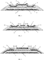
- FIG.1 is a schematic structure diagram of a thin film transistor having a double-gate structure in the prior art.
- an upper gate electrode 1 of the thin film transistor is overlapped on a source electrode 2 and a drain electrode 3.
- the voltages of the upper gate electrode 1 and the lower gate electrode 4 both reach a turn-on voltage (the turn-on voltage is a threshold voltage, and when a voltage of a gate electrode is greater than the turn-on voltage, a conducting channel can be formed in the semiconductor layer by induction), an upper conducting channel and a lower conducting channel which are parallel to each other can be formed in the semiconductor layer 5 by induction.
- the drain electrode 3 can be conducted with the source electrode 2 separately by the upper conducting channel.
- the drain electrode 3 can also be conducted with the source electrode 2 separately by the lower conducting channel.
- embodiments of the present invention provide a thin film transistor and a preparation method thereof, to solve the problem that it is difficult to achieve simultaneous conduction of an upper conducting channel and a lower conducting channel for an upper gate electrode and a lower gate electrode of the thin film transistors in the prior art.
- Embodiments of the present invention provide a thin film transistor, the thin film transistor comprises an upper gate electrode, a lower gate electrode, an upper insulating layer, a lower insulating layer, a semiconductor layer, a source electrode and a drain electrode.
- the lower insulating layer is arranged on the lower gate electrode; the semiconductor layer is arranged on the lower insulating layer, the semiconductor layer is respectively lapped with the source electrode and the drain electrode, the upper insulating layer is covered on the semiconductor layer, and the upper gate electrode is arranged on the upper insulating layer.
- Embodiments of the present invention further provide a method for preparing a thin film transistor, comprising the steps of:
- the conduction of the upper conducting channel cannot be independently realized by the upper gate electrode. Only when the voltage of the lower gate electrode reaches a turn-on voltage, the conduction of the upper conducting channel can be indirectly achieved by the lower conducting channel formed by the induction of the lower gate electrode, thereby achieving simultaneous conduction of the upper conducting channel and the lower conducting channel.
- FIG. 2 is a schematic structure diagram of a thin film transistor according to an embodiment of the present invention.
- the thin film transistor comprises an upper gate electrode 1, a lower gate electrode 4, an upper insulating layer 6, a lower insulating layer 7, a semiconductor layer 5, a source electrode 2 and a drain electrode 3.
- the lower insulating layer 7 is arranged on the lower gate electrode 4, the semiconductor layer 5 is arranged on the lower insulating layer 7, the semiconductor layer 5 is lapped with the source electrode 2 and the drain electrode 3, the upper insulating layer 6 covers the semiconductor layer 5, and the upper gate electrode 1 is arranged on the upper insulating layer 6.
- the way that the semiconductor layer 5 is lapped with the source electrode 2 and the drain electrode 3 can be adjusted according to actual structure design requirements, as long as the conduction of the conducting channel in the semiconductor layer 5 with the source electrode 2 and the drain electrode 3 can be realized.
- the way that the semiconductor layer 5 is lapped with the source electrode 2 and the drain electrode 3 is not limited in the present invention.
- a surface of the upper insulating layer 6 comprises a source electrode hole 14 and a drain electrode hole 15.
- the way that the semiconductor layer 5 is lapped with the source electrode 2 and the drain electrode 3 is as follows: the source electrode 2 is lapped with a surface of the semiconductor layer 5 by the source electrode hole 14 on the surface of the upper insulating layer 6, and the drain electrode 3 is lapped with the surface of the semiconductor layer 5 by the drain electrode hole 15 on the surface of the upper insulating layer 6.
- the upper gate electrode 1 is in a same layer as the source electrode 2 and the drain electrode 3, instead of being overlapped on the source electrode 2 and the drain electrode 3. Since in a plane parallel with the conducting channel in the semiconductor layer 5, there is the first gap 8 between the orthographic projection of the upper gate electrode 1 and the orthographic projection of the source electrode 2 and the second gap 9 between the orthographic projection of the upper gate electrode 1 and the orthographic projection of the drain electrode 3, regions in the semiconductor layer 5 corresponding to the first gap 8 and the second gap 9 are always in the high-resistance state.
- the upper gate electrode 1 is overlapped on the source electrode 2 and the drain electrode 3, it is necessary to separately design a passivation layer 16 to perform mask etching for the preparation of the upper gate electrode 1, thereby increasing preparation costs.
- the upper gate electrode 1 is in a same layer as the source electrode 2 and the drain electrode 3, and thus it is not necessary to separately design a single mask etching process for the preparation of the upper gate electrode 1.
- the upper gate electrode 1, the source electrode 2 and the drain electrode 3 can be synchronously formed by etching once, thereby saving the preparation costs.
- FIG. 3 is a schematic structure diagram of a thin film transistor according to another embodiment of the present invention. Unlike the structure shown in FIG. 2 , in the thin film transistor structure shown in FIG. 3 , the semiconductor layer 5 is lapped with the source electrode 2 and the drain electrode 3 in another way in which the simultaneous conduction of the upper conducting channel and the lower conducting channel can also be achieved. Specifically, the source electrode 2 and the drain electrode 3 are arranged on the lower insulating layer 7, and the semiconductor layer 5 is lapped with the surface of the source electrode 2, the surface of the drain electrode 3 and the surface of the lower insulating layer 7.
- the semiconductor layer 5 is generally thin to prevent an excessive parasitic resistance when the current from the source electrode 2/the drain electrode 3 breaks down the semiconductor layer 5 and reaches the conducting channel.
- the thickness of the semiconductor layer 5 can be set between 10 nm and 200 nm to ensure that the upper conducting channel and the lower conducting channel in the semiconductor layer 5 can be simultaneously conducted without influencing each other.
- the thickness of the semiconductor layer 5 can be specifically set to be 30 nm. Such a thickness can ensure that sufficiently wide conducting channels are formed on the upper and lower surfaces on the semiconductor layer 5, and that parasitic resistance generated when the source electrode 2/the drain electrode 3 is lapped with the conducting channel can be decreased as much as possible.
- the first gap 8 between the orthographic projection of the upper gate electrode 1 and the orthographic projection of the source electrode 2, and there is the second gap 9 between the orthographic projection of the upper gate electrode 1 and the orthographic projection of the drain electrode 3.
- the width of the first gap 8 corresponds to a first semiconductor material high-resistance region
- the width of the second gap 9 corresponds to a second semiconductor material high-resistance region.
- the width of the first gap 8 and the width of the second gap 9 can be adjusted according to an intrinsic resistance of semiconductor material of the semiconductor layer 5 and a minimum leakage current that the semiconductor material can withstand.
- the drain voltage U d is 10 V
- the width W of the semiconductor layer 5 is 5 um
- the width D of the first gap 8/the second gap 9 is 1 um which is a process limit value for processing the first gap 8/the second gap 9 between the upper gate electrode 1 and the source electrode 2/the drain electrode 3
- the leakage current I leak thus obtained is 0.5 pA, which can meet the requirements on OLED devices.
- the minimum width of the first gap 8/the second gap 9 between the upper gate electrode 1 and the source electrode 2/the drain electrode 3 can be 1 um.
- the width of the first gap 8 and the width of the second gap 9 can be specifically set to be 3 um, which can ensure that a lithography machine operates under stable process conditions and realizes a relatively high process precision, and that the leakage current of the upper gate electrode 1 can be controlled within a magnitude of 1pA and also meet the requirements for OLED devices.
- the width of the first gap 8 and the width of the second gap 9 are not strictly limited in the present invention.
- the semiconductor layer 5 can be made of semiconductor material such as metal oxides (for example, IGZO), or noncrystalline silicon, or polycrystalline silicon or microcrystalline silicon material. Material for preparing the semiconductor layer 5 is not limited in the present invention.
- the upper gate electrode 1, the lower gate electrode 4, the source electrode 2 and the drain electrode 3 can be made of Mo metal material or other conducting material.
- the material for preparing the upper gate electrode 1, the lower gate electrode 4, the source electrode 2 and the drain electrode 3 is not limited in the present invention either.
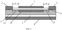
- FIG. 4 is a schematic view illustrating the conducting principle of a thin film transistor according to an embodiment of the present invention.
- the semiconductor layer 5 is lapped with the source electrode 2 and the drain electrode 3 in the way shown in FIG.2 . Since the voltage of the lower gate electrode 4 has not yet reached the turn-on voltage of the lower gate electrode 4, the conduction of the lower conducting channel cannot be achieved in the semiconductor layer 5.
- FIG. 5 is a schematic view illustrating the conducting principle of a thin film transistor according to an embodiment of the present invention.
- the semiconductor layer 5 is lapped with the source electrode 2 and the drain electrode 3 in the way shown in FIG.2 .
- the voltage of the lower gate electrode 4 has reached the turn-on voltage of the lower gate electrode 4, the flow direction of the current in the semiconductor layer 5 is shown by the arrow in the drawing. Specifically, since the voltage of the lower gate electrode 4 has reached the turn-on voltage of the lower gate electrode 4, the lower conducting channel 11 has been formed in the semiconductor layer 5.
- the current can break down the semiconductor layer 5 from the drain electrode 3 and reach the lower conducting channel 11, and can break down the semiconductor layer 5 again via the lower conducting channel 11 and flow towards the source electrode 2.
- the voltage of the upper gate electrode 1 also reaches the turn-on voltage of the upper gate electrode 1
- the current can break down the semiconductor layer 5 from the lower conducting channel 11 and reach the upper conducting channel 10, and can break down the semiconductor layer 5 again via the upper conducting channel 10 and finally flow towards the source electrode 2.
- simultaneous conduction of the upper conducting channel 10 and the lower conducting channel 11 is achieved, thereby improving the mobility.
- an operator can set the circuit structures of the upper gate electrode 1 and the lower gate electrode 4 in various ways. For example, an operator can independently set the upper gate electrode 1 and the lower gate electrode 4 in the circuit structures without parallel arranging, so that the voltage of the upper gate electrode 1 is always higher than the turn-on voltage of the upper gate electrode 1. However, due to the first gap 8 and the second gap 9, the upper conducting channel 10 will not be conducted with the source electrode 2 and the drain electrode 3.
- the upper gate electrode 1 can be indirectly conducted with the upper conducting channel 10 by the lower conducting channel 11 formed by induction of the lower gate electrode 4.
- the method for arranging respective circuit structures of the upper gate electrode 1 and the lower gate electrode 4 is not limited in the present invention.
- FIG. 6 is a view showing results of a conducting test of a thin film transistor according to an embodiment of the present invention.
- Vg represents a voltage of the lower gate electrode 4
- Vth represents the turn-on voltage of the lower gate electrode 4
- represents the intensity of current conducted in the semiconductor layer 5.
- the ratio means a ratio of the mobility of the thin film transistor of the present invention to the mobility of a thin film transistor with a traditional single-gate structure.
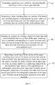
- FIG. 7 is a schematic flowchart of a method for preparing a thin film transistor according to an embodiment of the present invention.
- the semiconductor layer 5 in the formed thin film transistor is lapped with the source electrode 2 and the drain electrode 3 in the lapping way as shown in FIG. 2 .
- the method for preparing the thin film transistor comprises the following steps.
- Step 701 A metal layer is deposited on a substrate, and the metal layer is patterned to form a lower gate electrode 4.
- a glass plate can be used as the substrate.
- Step 702 A lower insulating layer 7 is deposited on a surface of the lower gate electrode 4 and a semiconductor layer 5 is deposited on a surface of the lower insulating layer 7, and then an upper insulating layer 6 is deposited on a surface of the semiconductor layer 5.
- this lower insulating layer 7 is fitted with the lower gate electrode 4 and the lower gate electrode 4 can also be called a gate electrode, this lower insulating layer 7 can also be called a gate insulating layer.
- the upper insulating layer 6 can also be called an etching stop layer (ESL).
- Step 703 A source electrode hole 14 and a drain electrode hole 15 are respectively formed by etching at positions corresponding to the source electrode 2 and the drain electrode 3 on a surface of the upper insulating layer 6, and bottoms of the source electrode hole 14 and the drain electrode hole 15 are communicated with the semiconductor layer 5. In this way, the source electrode 2 and the drain electrode 3 formed in the source electrode hole 14 and the drain electrode hole 15 in the following steps can be lapped with the semiconductor layer 5.
- Step 704 A metal layer is deposited on the surface of the upper insulating layer 6 and in the source electrode hole 14 and the drain electrode hole 15, and the metal layer is patterned to form the source electrode 2, the drain electrode 3 and an upper gate electrode 1, and in a plane which is parallel to a conducting channel in the semiconductor layer 5, there is a first gap 8 between an orthographic projection of the upper gate electrode 1 and an orthographic projection of the source electrode 2, and there is a second gap 9 between the orthographic projection of the upper gate electrode 1 and an orthographic projection of the drain electrode 3.
- the upper gate electrode 1, the source electrode 2 and the drain electrode 3 are located in the same layer, the upper gate electrode 1, the source electrode 2 and the drain electrode 3 can be synchronously formed by patterning once without designing a mask etching process for the preparation of the upper gate electrode 1. The preparation cost is therefore saved.
- a passivation layer or an anode can be deposited or other processes such as OLED preparation can be performed.
- the conduction of the upper conducting channel 10 cannot be independently realized by the upper gate electrode 1. Only when the voltage of the lower gate electrode 4 reaches a turn-on voltage, the conduction of the upper conducting channel 10 can be indirectly achieved by the lower conducting channel 11 formed by induction of the lower gate electrode 4. In this way, simultaneous conduction of the upper conducting channel and the lower conducting channel is achieved.
- the thin film transistor of the present invention is suitable to be industrially produced by exiting production equipment, and can be applied to liquid crystal display panels with high integration density and high resolution and other related technical products.
- the structure thereof improves the simultaneous conduction performance of the upper conducting channel and the lower conducting channel in the semiconductor layer.
- the method for preparing the thin film transistor of the present invention can make full use of existing production and processing equipment to form a production process.
- the method is applicable for large-scale industrial production.
- the resulting thin film transistors have a high mobility.
Landscapes
- Thin Film Transistor (AREA)
Abstract
Description
- The present invention claims priority of Chinese Patent Application No.
201510305703.X, filed on June 04, 2015 - The present invention relates to the technical field of optoelectronic display, and in particular to a thin film transistor and a preparation method thereof.
- In the prior art, in order to improve the mobility of thin film transistors, a double-gate structure, i.e., a structure with an upper gate electrode and a lower gate electrode, can be used to induce double channels at a semiconductor layer to enlarge a conducting pathway.
-
FIG.1 is a schematic structure diagram of a thin film transistor having a double-gate structure in the prior art. As shown inFIG. 1 , anupper gate electrode 1 of the thin film transistor is overlapped on asource electrode 2 and adrain electrode 3. When the voltages of theupper gate electrode 1 and thelower gate electrode 4 both reach a turn-on voltage (the turn-on voltage is a threshold voltage, and when a voltage of a gate electrode is greater than the turn-on voltage, a conducting channel can be formed in the semiconductor layer by induction), an upper conducting channel and a lower conducting channel which are parallel to each other can be formed in thesemiconductor layer 5 by induction. Since theupper gate electrode 1 is overlapped on thesource electrode 2 and thedrain electrode 3, that is, in a plane parallel with the conducting channel in thesemiconductor layer 5, an orthographic projection of theupper gate electrode 1 is partially overlapped with an orthographic projection of thesource electrode 2 and an orthographic projection of thedrain electrode 3 respectively, thedrain electrode 3 can be conducted with thesource electrode 2 separately by the upper conducting channel. In addition, thedrain electrode 3 can also be conducted with thesource electrode 2 separately by the lower conducting channel. However, for thin film transistors with such a double-gate structure, it is difficult to ensure the improvement of mobility by simultaneous conduction of the upper conducting channel and the lower conducting channel. - Because of process technologies, it is difficult to match parameters such as capacitance of an upper
insulating layer 6 below theupper gate electrode 1 and a lowerinsulating layer 7 above the lower gate electrode. This will result in different turn-on voltages of the upper conducting channel and the lower conducting channel respectively formed in theupper gate electrode 1 and thelower gate electrode 4. Thus, it is difficult to achieve simultaneous conduction of the upper conducting channel and the lower conducting channel in the thin film transistor structure in the prior art. - Accordingly, embodiments of the present invention provide a thin film transistor and a preparation method thereof, to solve the problem that it is difficult to achieve simultaneous conduction of an upper conducting channel and a lower conducting channel for an upper gate electrode and a lower gate electrode of the thin film transistors in the prior art.
- Embodiments of the present invention provide a thin film transistor, the thin film transistor comprises an upper gate electrode, a lower gate electrode, an upper insulating layer, a lower insulating layer, a semiconductor layer, a source electrode and a drain electrode. The lower insulating layer is arranged on the lower gate electrode; the semiconductor layer is arranged on the lower insulating layer, the semiconductor layer is respectively lapped with the source electrode and the drain electrode, the upper insulating layer is covered on the semiconductor layer, and the upper gate electrode is arranged on the upper insulating layer. In a plane parallel with a conducting channel in the semiconductor layer, there is a first gap between an orthographic projection of the upper gate electrode and an orthographic projection of the source electrode, and there is a second gap between the orthographic projection of the upper gate electrode and an orthographic projection of the drain electrode.
- Embodiments of the present invention further provide a method for preparing a thin film transistor, comprising the steps of:
- depositing a metal layer on a substrate, and patterning the metal layer to form a lower gate electrode;
- depositing a lower insulating layer on a surface of the lower gate electrode, depositing a semiconductor layer on a surface of the lower insulating layer, and then depositing an upper insulating layer on a surface of the semiconductor layer;
- forming, by respectively etching, a source electrode hole and a drain electrode hole on a surface of the upper insulating layer at positions corresponding to a source electrode and a drain electrode, and bottoms of the source electrode hole and the drain electrode hole being communicated with the semiconductor layer; and
- depositing a metal layer on the surface of the upper insulating layer and in the source electrode hole and the drain electrode hole, and patterning the metal layer to form the source electrode, the drain electrode and an upper gate electrode, wherein in a plane parallel with a conducting channel in the semiconductor layer, there is a first gap between an orthographic projection of the upper gate electrode and an orthographic projection of the source electrode, and there is a second gap between the orthographic projection of the upper gate electrode and an orthographic projection of the drain electrode.
- For a thin film transistor according to the embodiments of the present invention, in a plane parallel with a conducting channel in the semiconductor layer, there is a first gap between an orthographic projection of the upper gate electrode and an orthographic projection of the source electrode, and there is a second gap between the orthographic projection of the upper gate electrode and an orthographic projection of the drain electrode. Thus, the conduction of the upper conducting channel cannot be independently realized by the upper gate electrode. Only when the voltage of the lower gate electrode reaches a turn-on voltage, the conduction of the upper conducting channel can be indirectly achieved by the lower conducting channel formed by the induction of the lower gate electrode, thereby achieving simultaneous conduction of the upper conducting channel and the lower conducting channel.
-
-
FIG.1 is a schematic structure diagram of a thin film transistor having a double-gate structure according to the prior art. -
FIG. 2 is a schematic structure diagram of a thin film transistor according to an embodiment of the present invention. -
FIG. 3 is a schematic structure diagram of a thin film transistor according to another embodiment of the present invention. -
FIG. 4 is a schematic view illustrating the conducting principle of a thin film transistor according to an embodiment of the present invention. -
FIG. 5 is a schematic view illustrating the conducting principle of a thin film transistor according to an embodiment of the present invention. -
FIG. 6 is a view showing results of a conducting test of a thin film transistor according to an embodiment of the present invention. -
FIG. 7 is a schematic flowchart of a method for preparing a thin film transistor according to an embodiment of the present invention. -
- 1 upper gate electrode
- 4 lower gate electrode
- 6 upper insulating layer
- 7 lower insulating layer
- 5 semiconductor layer
- 2 source electrode
- 3 drain electrode
- 8 first gap
- 9 second gap
- 10 upper conducting channel
- 11 lower conducting channel
- 12 first semiconductor material high-resistance region
- 13 second semiconductor material high-resistance region
- 14 source electrode hole
- 15 drain electrode hole
- 16 passivation layer.
- In order to make purposes, technical solutions and advantages of the present invention clearer, the present invention will be further described in detail with reference to the accompanying drawings.
-
FIG. 2 is a schematic structure diagram of a thin film transistor according to an embodiment of the present invention. As shown inFIG. 2 , the thin film transistor comprises anupper gate electrode 1, alower gate electrode 4, an upperinsulating layer 6, a lowerinsulating layer 7, asemiconductor layer 5, asource electrode 2 and adrain electrode 3. The lowerinsulating layer 7 is arranged on thelower gate electrode 4, thesemiconductor layer 5 is arranged on the lowerinsulating layer 7, thesemiconductor layer 5 is lapped with thesource electrode 2 and thedrain electrode 3, the upperinsulating layer 6 covers thesemiconductor layer 5, and theupper gate electrode 1 is arranged on the upper insulatinglayer 6. In a plane parallel to a conducting channel in thesemiconductor layer 5, there is afirst gap 8 between an orthographic projection of theupper gate electrode 1 and an orthographic projection of thesource electrode 2, and there is asecond gap 9 between the orthographic projection of theupper gate electrode 1 and an orthographic projection of thedrain electrode 3. - It can be understood by a person skilled in the art that the way that the
semiconductor layer 5 is lapped with thesource electrode 2 and thedrain electrode 3 can be adjusted according to actual structure design requirements, as long as the conduction of the conducting channel in thesemiconductor layer 5 with thesource electrode 2 and thedrain electrode 3 can be realized. The way that thesemiconductor layer 5 is lapped with thesource electrode 2 and thedrain electrode 3 is not limited in the present invention. - In an embodiment of the present invention, as shown in
FIG. 2 , a surface of the upperinsulating layer 6 comprises asource electrode hole 14 and adrain electrode hole 15. The way that thesemiconductor layer 5 is lapped with thesource electrode 2 and thedrain electrode 3 is as follows: thesource electrode 2 is lapped with a surface of thesemiconductor layer 5 by thesource electrode hole 14 on the surface of the upperinsulating layer 6, and thedrain electrode 3 is lapped with the surface of thesemiconductor layer 5 by thedrain electrode hole 15 on the surface of the upperinsulating layer 6. It can be seen that, unlike the thin film transistor having a double-gate structure (i.e., a structure with an upper gate electrode and a lower gate electrode) in the prior art, when using the above lapping method, theupper gate electrode 1 is in a same layer as thesource electrode 2 and thedrain electrode 3, instead of being overlapped on thesource electrode 2 and thedrain electrode 3. Since in a plane parallel with the conducting channel in thesemiconductor layer 5, there is thefirst gap 8 between the orthographic projection of theupper gate electrode 1 and the orthographic projection of thesource electrode 2 and thesecond gap 9 between the orthographic projection of theupper gate electrode 1 and the orthographic projection of thedrain electrode 3, regions in thesemiconductor layer 5 corresponding to thefirst gap 8 and thesecond gap 9 are always in the high-resistance state. In this way, even the voltage of theupper gate electrode 1 reaches a turn-on voltage and an upper conducting channel in the low-resistance state is formed by induction of thesemiconductor layer 5 corresponding to theupper gate electrode 1, it is unable to achieve the conduction between the upper conducting channel and thesource electrode 2 and drainelectrode 3. Only when the voltage of thelower gate electrode 4 reaches the turn-on voltage, the conduction of the upper conducting channel can be indirectly achieved by the lower conducting channel formed by induction of thelower gate electrode 4, thereby achieving simultaneous conduction of the upper conducting channel and the lower conducting channel. - In addition, as shown in
FIG.1 , in the prior art, since theupper gate electrode 1 is overlapped on thesource electrode 2 and thedrain electrode 3, it is necessary to separately design apassivation layer 16 to perform mask etching for the preparation of theupper gate electrode 1, thereby increasing preparation costs. However, when a structure of the thin film transistor shown inFIG. 2 is used, theupper gate electrode 1 is in a same layer as thesource electrode 2 and thedrain electrode 3, and thus it is not necessary to separately design a single mask etching process for the preparation of theupper gate electrode 1. Theupper gate electrode 1, thesource electrode 2 and thedrain electrode 3 can be synchronously formed by etching once, thereby saving the preparation costs. -
FIG. 3 is a schematic structure diagram of a thin film transistor according to another embodiment of the present invention. Unlike the structure shown inFIG. 2 , in the thin film transistor structure shown inFIG. 3 , thesemiconductor layer 5 is lapped with thesource electrode 2 and thedrain electrode 3 in another way in which the simultaneous conduction of the upper conducting channel and the lower conducting channel can also be achieved. Specifically, thesource electrode 2 and thedrain electrode 3 are arranged on the lower insulatinglayer 7, and thesemiconductor layer 5 is lapped with the surface of thesource electrode 2, the surface of thedrain electrode 3 and the surface of the lower insulatinglayer 7. In this way, when the voltages of theupper gate electrode 1 and thelower gate electrode 4 both reach the turn-on voltage, an upper conducting channel and a lower conducting channel which are parallel to each other can be formed in thesemiconductor layer 5 by induction, and the simultaneous conduction of the upper and lower conducting channels with thesource electrode 2 and thedrain electrode 3 can be achieved. - In an embodiment of the present invention, the
semiconductor layer 5 is generally thin to prevent an excessive parasitic resistance when the current from thesource electrode 2/thedrain electrode 3 breaks down thesemiconductor layer 5 and reaches the conducting channel. However, since the depth of the conducting channel is between 3 nm and 15 nm in the ON-state, the thickness of thesemiconductor layer 5 can be set between 10 nm and 200 nm to ensure that the upper conducting channel and the lower conducting channel in thesemiconductor layer 5 can be simultaneously conducted without influencing each other. In an embodiment, the thickness of thesemiconductor layer 5 can be specifically set to be 30 nm. Such a thickness can ensure that sufficiently wide conducting channels are formed on the upper and lower surfaces on thesemiconductor layer 5, and that parasitic resistance generated when thesource electrode 2/thedrain electrode 3 is lapped with the conducting channel can be decreased as much as possible. - As mentioned above, in a plane parallel with a conducting channel in the
semiconductor layer 5, there is thefirst gap 8 between the orthographic projection of theupper gate electrode 1 and the orthographic projection of thesource electrode 2, and there is thesecond gap 9 between the orthographic projection of theupper gate electrode 1 and the orthographic projection of thedrain electrode 3. The width of thefirst gap 8 corresponds to a first semiconductor material high-resistance region, and the width of thesecond gap 9 corresponds to a second semiconductor material high-resistance region. To ensure that there is a semiconductor material high-resistance region between theupper conducting channel 10 and thesource electrode 2 as well as thedrain electrode 3, and that the volume of the thin film transistor is reduced as much as possible, the width of thefirst gap 8 and the width of thesecond gap 9 can be adjusted according to an intrinsic resistance of semiconductor material of thesemiconductor layer 5 and a minimum leakage current that the semiconductor material can withstand. When the voltage of thelower gate electrode 4 has not reached the turn-on voltage while the voltage of the upper gate electrode has already reached the turn-on voltage, the leakage current flowing through thesemiconductor layer 5 can be expressed by Ileak = Ud/(2R*W/D), where Ud is a drain voltage, R is an intrinsic resistance of thesemiconductor layer 5, W is the width of thesemiconductor layer 5, and Dum is the width of thefirst gap 8/thesecond gap 9. - In an embodiment of the present invention, when the intrinsic sheet resistance R of the semiconductor material (for example, metal oxides) selected for the
semiconductor layer 5 can reach 1e+ 12 Ω, the drain voltage Ud is 10 V, the width W of thesemiconductor layer 5 is 5 um, and the width D of thefirst gap 8/thesecond gap 9 is 1 um which is a process limit value for processing thefirst gap 8/thesecond gap 9 between theupper gate electrode 1 and thesource electrode 2/thedrain electrode 3, the leakage current Ileak thus obtained is 0.5 pA, which can meet the requirements on OLED devices. Thus, the minimum width of thefirst gap 8/thesecond gap 9 between theupper gate electrode 1 and thesource electrode 2/thedrain electrode 3 can be 1 um. In an embodiment of the present invention, the width of thefirst gap 8 and the width of thesecond gap 9 can be specifically set to be 3 um, which can ensure that a lithography machine operates under stable process conditions and realizes a relatively high process precision, and that the leakage current of theupper gate electrode 1 can be controlled within a magnitude of 1pA and also meet the requirements for OLED devices. The width of thefirst gap 8 and the width of thesecond gap 9 are not strictly limited in the present invention. - In an embodiment of the present invention, the
semiconductor layer 5 can be made of semiconductor material such as metal oxides (for example, IGZO), or noncrystalline silicon, or polycrystalline silicon or microcrystalline silicon material. Material for preparing thesemiconductor layer 5 is not limited in the present invention. - In an embodiment of the present invention, the
upper gate electrode 1, thelower gate electrode 4, thesource electrode 2 and thedrain electrode 3 can be made of Mo metal material or other conducting material. The material for preparing theupper gate electrode 1, thelower gate electrode 4, thesource electrode 2 and thedrain electrode 3 is not limited in the present invention either. -
FIG. 4 is a schematic view illustrating the conducting principle of a thin film transistor according to an embodiment of the present invention. As shown inFIG. 4 , thesemiconductor layer 5 is lapped with thesource electrode 2 and thedrain electrode 3 in the way shown inFIG.2 . Since the voltage of thelower gate electrode 4 has not yet reached the turn-on voltage of thelower gate electrode 4, the conduction of the lower conducting channel cannot be achieved in thesemiconductor layer 5. Thus, even the voltage of theupper gate electrode 1 has reached the turn-on voltage of theupper gate electrode 1, since theupper gate electrode 1 is in a same layer as thesource electrode 2 and thedrain electrode 3 and overlapped with a part of the upper insulatinglayer 6 instead of being overlapped on thesource electrode 2 and thedrain electrode 3, and since there is thefirst gap 8 between theupper gate electrode 1 and thesource electrode 2 and thesecond gap 9 between theupper gate electrode 1 and thedrain electrode 3, only a relatively short upper conductingchannel 10 corresponding to theupper gate electrode 1 can be formed in thesemiconductor layer 5 by induction of theupper gate electrode 1. There is a semiconductor material high-resistance region 12 corresponding to thefirst gap 8 between this upper conductingchannel 10 and thesource electrode 2 and a semiconductor material high-resistance region 13 corresponding to thesecond gap 9 between this upper conductingchannel 10 and thedrain electrode 3. Thus, this upper conductingchannel 10 cannot be conducted with thesource electrode 2 and thedrain electrode 3. It can be seen that, when the voltage of thelower gate electrode 4 does not reach the turn-on voltage of thelower gate electrode 4, theupper conducting channel 10 cannot be conducted with thesource electrode 2 and thedrain electrode 3 no matter whether the voltage of theupper gate electrode 1 reaches the turn-on voltage of theupper gate electrode 1 or not. -
FIG. 5 is a schematic view illustrating the conducting principle of a thin film transistor according to an embodiment of the present invention. As shown inFIG. 5 , thesemiconductor layer 5 is lapped with thesource electrode 2 and thedrain electrode 3 in the way shown inFIG.2 . The voltage of thelower gate electrode 4 has reached the turn-on voltage of thelower gate electrode 4, the flow direction of the current in thesemiconductor layer 5 is shown by the arrow in the drawing. Specifically, since the voltage of thelower gate electrode 4 has reached the turn-on voltage of thelower gate electrode 4, thelower conducting channel 11 has been formed in thesemiconductor layer 5. Due to the small thickness of thesemiconductor layer 5, the current can break down thesemiconductor layer 5 from thedrain electrode 3 and reach thelower conducting channel 11, and can break down thesemiconductor layer 5 again via thelower conducting channel 11 and flow towards thesource electrode 2. At this point, when the voltage of theupper gate electrode 1 also reaches the turn-on voltage of theupper gate electrode 1, the current can break down thesemiconductor layer 5 from thelower conducting channel 11 and reach theupper conducting channel 10, and can break down thesemiconductor layer 5 again via theupper conducting channel 10 and finally flow towards thesource electrode 2. Thus, simultaneous conduction of theupper conducting channel 10 and thelower conducting channel 11 is achieved, thereby improving the mobility. - It can be understood by a person skilled in the art that, in order to achieve simultaneous conduction of the
upper conducting channel 10 and thelower conducting channel 11, an operator can set the circuit structures of theupper gate electrode 1 and thelower gate electrode 4 in various ways. For example, an operator can independently set theupper gate electrode 1 and thelower gate electrode 4 in the circuit structures without parallel arranging, so that the voltage of theupper gate electrode 1 is always higher than the turn-on voltage of theupper gate electrode 1. However, due to thefirst gap 8 and thesecond gap 9, theupper conducting channel 10 will not be conducted with thesource electrode 2 and thedrain electrode 3. Only when the voltage of thelower gate electrode 4 reaches the turn-on voltage of thelower gate electrode 4, theupper gate electrode 1 can be indirectly conducted with theupper conducting channel 10 by thelower conducting channel 11 formed by induction of thelower gate electrode 4. The method for arranging respective circuit structures of theupper gate electrode 1 and thelower gate electrode 4 is not limited in the present invention. -
FIG. 6 is a view showing results of a conducting test of a thin film transistor according to an embodiment of the present invention. As shown inFIG. 6 , Vg represents a voltage of thelower gate electrode 4, Vth represents the turn-on voltage of thelower gate electrode 4, and |Id| represents the intensity of current conducted in thesemiconductor layer 5. The ratio means a ratio of the mobility of the thin film transistor of the present invention to the mobility of a thin film transistor with a traditional single-gate structure. The test conditions are the drain voltage Vd=0.1 V and Vg=-10 ∼ 20 V. It can be seen fromFIG. 6 that the thin film transistor structure according to the embodiments of the present invention can obtain a mobility of more than twice of that of the traditional single-gate thin film transistor. -
FIG. 7 is a schematic flowchart of a method for preparing a thin film transistor according to an embodiment of the present invention. Thesemiconductor layer 5 in the formed thin film transistor is lapped with thesource electrode 2 and thedrain electrode 3 in the lapping way as shown inFIG. 2 . As shown inFIG.7 , the method for preparing the thin film transistor comprises the following steps. - Step 701: A metal layer is deposited on a substrate, and the metal layer is patterned to form a
lower gate electrode 4. Here, a glass plate can be used as the substrate. - Step 702: A lower insulating
layer 7 is deposited on a surface of thelower gate electrode 4 and asemiconductor layer 5 is deposited on a surface of the lower insulatinglayer 7, and then an upper insulatinglayer 6 is deposited on a surface of thesemiconductor layer 5. - In an embodiment of the present invention, since the lower insulating
layer 7 is fitted with thelower gate electrode 4 and thelower gate electrode 4 can also be called a gate electrode, this lower insulatinglayer 7 can also be called a gate insulating layer. - In an embodiment of the present invention, since the
source electrode hole 14 and thedrain electrode hole 15 are to be formed by etching in the following steps, the upper insulatinglayer 6 can also be called an etching stop layer (ESL). - Step 703: A
source electrode hole 14 and adrain electrode hole 15 are respectively formed by etching at positions corresponding to thesource electrode 2 and thedrain electrode 3 on a surface of the upper insulatinglayer 6, and bottoms of thesource electrode hole 14 and thedrain electrode hole 15 are communicated with thesemiconductor layer 5. In this way, thesource electrode 2 and thedrain electrode 3 formed in thesource electrode hole 14 and thedrain electrode hole 15 in the following steps can be lapped with thesemiconductor layer 5. - Step 704: A metal layer is deposited on the surface of the upper insulating
layer 6 and in thesource electrode hole 14 and thedrain electrode hole 15, and the metal layer is patterned to form thesource electrode 2, thedrain electrode 3 and anupper gate electrode 1, and in a plane which is parallel to a conducting channel in thesemiconductor layer 5, there is afirst gap 8 between an orthographic projection of theupper gate electrode 1 and an orthographic projection of thesource electrode 2, and there is asecond gap 9 between the orthographic projection of theupper gate electrode 1 and an orthographic projection of thedrain electrode 3. It can be seen that, since theupper gate electrode 1, thesource electrode 2 and thedrain electrode 3 are located in the same layer, theupper gate electrode 1, thesource electrode 2 and thedrain electrode 3 can be synchronously formed by patterning once without designing a mask etching process for the preparation of theupper gate electrode 1. The preparation cost is therefore saved. On the resulting thin film transistor, a passivation layer or an anode can be deposited or other processes such as OLED preparation can be performed. - For the thin film transistor according to the embodiments of the present invention, in a plane which is parallel to a conducting channel in the
semiconductor layer 5, there is thefirst gap 8 between the orthographic projection of theupper gate electrode 1 and the orthographic projection of thesource electrode 2, and there is thesecond gap 9 between the orthographic projection of theupper gate electrode 1 and the orthographic projection of thedrain electrode 3. In this way, the conduction of theupper conducting channel 10 cannot be independently realized by theupper gate electrode 1. Only when the voltage of thelower gate electrode 4 reaches a turn-on voltage, the conduction of theupper conducting channel 10 can be indirectly achieved by thelower conducting channel 11 formed by induction of thelower gate electrode 4. In this way, simultaneous conduction of the upper conducting channel and the lower conducting channel is achieved. - The foregoing descriptions are merely preferred embodiments of the present invention and not intended to limit the present invention. Any modifications, equivalent replacements and improvements made within the spirit and principle of the present invention shall fall into the protection scope of the present invention.
- The thin film transistor of the present invention is suitable to be industrially produced by exiting production equipment, and can be applied to liquid crystal display panels with high integration density and high resolution and other related technical products. The structure thereof improves the simultaneous conduction performance of the upper conducting channel and the lower conducting channel in the semiconductor layer.
- The method for preparing the thin film transistor of the present invention can make full use of existing production and processing equipment to form a production process. The method is applicable for large-scale industrial production. The resulting thin film transistors have a high mobility.
Claims (10)
- A thin film transistor, comprising an upper gate electrode (1), a lower gate electrode (4), an upper insulating layer (6), a lower insulating layer (7), a semiconductor layer (5), a source electrode (2) and a drain electrode (3), wherein the lower insulating layer (7) is arranged on the lower gate electrode (4), the semiconductor layer (5) is arranged on the lower insulating layer (7), the semiconductor layer (5) is respectively lapped with the source electrode (2) and the drain electrode (3), the upper insulating layer (6) covers the semiconductor layer (5), and the upper gate electrode (1) is arranged on the upper insulating layer (6), and
wherein, in a plane parallel to a conducting channel in the semiconductor layer (5), there is a first gap (8) between an orthographic projection of the upper gate electrode (1) and an orthographic projection of the source electrode (2), and there is a second gap (9) between the orthographic projection of the upper gate electrode (1) and an orthographic projection of the drain electrode (3). - The thin film transistor according to claim 1, wherein a surface of the upper insulating layer (6) comprises a source electrode hole (14) and a drain electrode hole (15),
the source electrode (2) is lapped with a surface of the semiconductor layer (5) by the source electrode hole (14), and
the drain electrode (3) is lapped with the surface of the semiconductor layer (5) by the drain electrode hole (15). - The thin film transistor according to claim 1, wherein the source electrode (2) and the drain electrode (3) are arranged on the lower insulating layer (7), and the semiconductor layer (5) is lapped with a surface of the source electrode (2), a surface of the drain electrode (3) and a surface of the lower insulating layer (7).
- The thin film transistor according to claim 1, wherein, when in use, a voltage of the upper gate electrode (1) is maintained higher than a turn-on voltage of the upper gate electrode (1).
- The thin film transistor according to claim 1, wherein a width of the first gap (8) or a width of the second gap (9) is adjusted according to an intrinsic resistance of semiconductor material of the semiconductor layer (5) and a minimum leakage current that the semiconductor material can withstand.
- The thin film transistor according to claim 5, wherein the width of the first gap (8) and/or the width of the second gap (9) are greater than 1 um.
- The thin film transistor according to claim 5, wherein the width of the first gap (8) and/or the width of the second gap (9) are 3 um.
- The thin film transistor according to claim 1, wherein a thickness of the semiconductor layer (5) is 30 nm.
- A method for preparing the thin film transistor according to claim 2, comprising the steps of:depositing a metal layer on a substrate, and patterning the metal layer to form a lower gate electrode (4);depositing a lower insulating layer (7) on a surface of the lower gate electrode (4), depositing a semiconductor layer (5) on a surface of the lower insulating layer (7), and then depositing an upper insulating layer (6) on a surface of the semiconductor layer (5);forming a source electrode hole (14) and a drain electrode hole (15) on a surface of the upper insulating layer (6) by etching at positions corresponding to a source electrode (2) and a drain electrode (3), bottoms of the source electrode hole (14) and the drain electrode hole (15) being communicated with the semiconductor layer (5); anddepositing a metal layer on the surface of the upper insulating layer (6) and in the source electrode hole and the drain electrode hole, and patterning the metal layer to form the source electrode (2), the drain electrode (3) and an upper gate electrode (1), wherein in a plane parallel to a conducting channel in the semiconductor layer (5), there is a first gap (8) between an orthographic projection of the upper gate electrode (1) and an orthographic projection of the source electrode (2), and there is a second gap (9) between the orthographic projection of the upper gate electrode (1) and an orthographic projection of the drain electrode (3).
- The method according to claim 9, wherein the upper gate electrode, the source electrode and the drain electrode are synchronously formed by patterning once.
Applications Claiming Priority (2)
| Application Number | Priority Date | Filing Date | Title |
|---|---|---|---|
| CN201510305703.XA CN106298883B (en) | 2015-06-04 | 2015-06-04 | A kind of thin film transistor and preparation method thereof |
| PCT/CN2016/084245 WO2016192624A1 (en) | 2015-06-04 | 2016-06-01 | Thin film transistor and manufacturing method thereof |
Publications (2)
| Publication Number | Publication Date |
|---|---|
| EP3306669A1 true EP3306669A1 (en) | 2018-04-11 |
| EP3306669A4 EP3306669A4 (en) | 2018-06-27 |
Family
ID=57440152
Family Applications (1)
| Application Number | Title | Priority Date | Filing Date |
|---|---|---|---|
| EP16802547.6A Ceased EP3306669A4 (en) | 2015-06-04 | 2016-06-01 | Thin film transistor and manufacturing method thereof |
Country Status (7)
| Country | Link |
|---|---|
| US (1) | US10665725B2 (en) |
| EP (1) | EP3306669A4 (en) |
| JP (1) | JP6541803B2 (en) |
| KR (1) | KR102017228B1 (en) |
| CN (1) | CN106298883B (en) |
| TW (1) | TWI578521B (en) |
| WO (1) | WO2016192624A1 (en) |
Cited By (1)
| Publication number | Priority date | Publication date | Assignee | Title |
|---|---|---|---|---|
| US10665725B2 (en) | 2015-06-04 | 2020-05-26 | Kunshan New Flat Panel Display Technology Center Co., Ltd. | Thin film transistor |
Families Citing this family (3)
| Publication number | Priority date | Publication date | Assignee | Title |
|---|---|---|---|---|
| JP6822114B2 (en) * | 2016-12-13 | 2021-01-27 | 天馬微電子有限公司 | How to drive display devices, transistor circuits and thin film transistors |
| CN109585297A (en) * | 2018-10-22 | 2019-04-05 | 惠科股份有限公司 | A kind of manufacturing method of display panel and display panel |
| CN109585298A (en) | 2018-10-22 | 2019-04-05 | 惠科股份有限公司 | Display panel and manufacturing method thereof |
Family Cites Families (23)
| Publication number | Priority date | Publication date | Assignee | Title |
|---|---|---|---|---|
| JPH07249778A (en) * | 1994-03-08 | 1995-09-26 | Sony Corp | Display element driving device and manufacturing method thereof |
| KR20010032543A (en) * | 1997-11-28 | 2001-04-25 | 모리시타 요이찌 | Reflection-type display device and image device using reflection-type display device |
| JP2006237624A (en) * | 1998-06-12 | 2006-09-07 | Semiconductor Energy Lab Co Ltd | Semiconductor device and inverter circuit |
| JP3408762B2 (en) * | 1998-12-03 | 2003-05-19 | シャープ株式会社 | Semiconductor device having SOI structure and method of manufacturing the same |
| TWI313059B (en) * | 2000-12-08 | 2009-08-01 | Sony Corporatio | |
| CN1268004C (en) * | 2003-09-22 | 2006-08-02 | 东南大学 | Double-grid high-voltage N-type Mos transistor |
| TWI295855B (en) * | 2006-03-03 | 2008-04-11 | Ind Tech Res Inst | Double gate thin-film transistor and method for forming the same |
| CN100533803C (en) * | 2006-05-10 | 2009-08-26 | 财团法人工业技术研究院 | Circuit structure with double-gate organic thin film transistor and application thereof |
| KR100878066B1 (en) * | 2007-05-25 | 2009-01-13 | 재단법인서울대학교산학협력재단 | Flat panel display |
| KR100839893B1 (en) | 2008-03-07 | 2008-06-19 | 조인셋 주식회사 | Solderable Elastic Electrical Contact Terminals |
| WO2010047217A1 (en) * | 2008-10-24 | 2010-04-29 | Semiconductor Energy Laboratory Co., Ltd. | Semiconductor device and method for manufacturing the same |
| KR101432764B1 (en) * | 2008-11-13 | 2014-08-21 | 가부시키가이샤 한도오따이 에네루기 켄큐쇼 | Method for manufacturing semiconductor device |
| KR20110037220A (en) * | 2009-10-06 | 2011-04-13 | 삼성모바일디스플레이주식회사 | An organic light emitting display device comprising a thin film transistor, a method of manufacturing the same, and a thin film transistor |
| KR101523358B1 (en) * | 2009-12-04 | 2015-05-27 | 가부시키가이샤 한도오따이 에네루기 켄큐쇼 | Display device |
| WO2011074338A1 (en) * | 2009-12-17 | 2011-06-23 | シャープ株式会社 | Semiconductor device, active matrix substrate and display device |
| KR101152575B1 (en) * | 2010-05-10 | 2012-06-01 | 삼성모바일디스플레이주식회사 | Pixel circuit of a flat panel display device and method of driving the same |
| JP2012033835A (en) * | 2010-08-03 | 2012-02-16 | Canon Inc | Driving method of photoelectric element and photoelectric device driven by the driving method |
| TWI742574B (en) * | 2013-05-16 | 2021-10-11 | 日商半導體能源研究所股份有限公司 | Semiconductor device |
| WO2014200190A1 (en) * | 2013-06-11 | 2014-12-18 | 경희대학교 산학협력단 | Oxide semiconductor transistor used as pixel element of display device and manufacturing method therefor |
| KR20140144566A (en) * | 2013-06-11 | 2014-12-19 | 경희대학교 산학협력단 | Oxide semiconductor transistor used for pixel element of display device and method for manufacturing the same |
| KR20150061302A (en) * | 2013-11-27 | 2015-06-04 | 삼성디스플레이 주식회사 | Display substrates, methods of manufacturing the same and display devices including the same |
| CN104409512A (en) * | 2014-11-11 | 2015-03-11 | 深圳市华星光电技术有限公司 | Low-temperature polycrystalline silicon thin-film transistor based on dual-gate structure and preparation method thereof |
| CN106298883B (en) | 2015-06-04 | 2020-09-15 | 昆山工研院新型平板显示技术中心有限公司 | A kind of thin film transistor and preparation method thereof |
-
2015
- 2015-06-04 CN CN201510305703.XA patent/CN106298883B/en active Active
-
2016
- 2016-06-01 JP JP2017563061A patent/JP6541803B2/en active Active
- 2016-06-01 EP EP16802547.6A patent/EP3306669A4/en not_active Ceased
- 2016-06-01 KR KR1020177036339A patent/KR102017228B1/en active Active
- 2016-06-01 WO PCT/CN2016/084245 patent/WO2016192624A1/en not_active Ceased
- 2016-06-02 TW TW105117319A patent/TWI578521B/en active
-
2017
- 2017-12-04 US US15/830,423 patent/US10665725B2/en active Active
Cited By (1)
| Publication number | Priority date | Publication date | Assignee | Title |
|---|---|---|---|---|
| US10665725B2 (en) | 2015-06-04 | 2020-05-26 | Kunshan New Flat Panel Display Technology Center Co., Ltd. | Thin film transistor |
Also Published As
| Publication number | Publication date |
|---|---|
| US10665725B2 (en) | 2020-05-26 |
| KR102017228B1 (en) | 2019-09-02 |
| JP2018518839A (en) | 2018-07-12 |
| TWI578521B (en) | 2017-04-11 |
| EP3306669A4 (en) | 2018-06-27 |
| CN106298883A (en) | 2017-01-04 |
| KR20180015659A (en) | 2018-02-13 |
| JP6541803B2 (en) | 2019-07-10 |
| WO2016192624A1 (en) | 2016-12-08 |
| US20180097119A1 (en) | 2018-04-05 |
| TW201711193A (en) | 2017-03-16 |
| CN106298883B (en) | 2020-09-15 |
Similar Documents
| Publication | Publication Date | Title |
|---|---|---|
| US10573640B2 (en) | Electro-static discharge assembly with semiconductor layer, array substrate and fabrication method thereof, and display panel | |
| CN102034873B (en) | Thin film transistor and method for manufacturing the same | |
| US10665725B2 (en) | Thin film transistor | |
| CN109686793A (en) | Thin film transistor (TFT) and preparation method, array substrate, display device | |
| US20180269311A1 (en) | Semiconductor super-junction power device and manufacturing method therefor | |
| CN105097841B (en) | The production method and TFT substrate of TFT substrate | |
| CN107068770A (en) | A kind of thin film transistor (TFT) and preparation method thereof, array base palte, display panel | |
| CN105679820B (en) | JFET and its manufacturing method | |
| CN107895726A (en) | Array substrate, manufacturing method thereof, and display device | |
| TW200834932A (en) | Semiconductor device, method for manufacturing semiconductor device, and electro-optical apparatus | |
| US8653531B2 (en) | Thin film transistor and display device | |
| CN108400168A (en) | LDMOS device and its manufacturing method | |
| CN104465673B (en) | Array base palte and its manufacture method and display device | |
| CN108122759A (en) | Thin film transistor (TFT) and preparation method thereof, array substrate and display device | |
| KR101829805B1 (en) | Oxide semiconductor transistor and manufacturing the same | |
| CN104934444B (en) | Coplanar type oxide semiconductor TFT substrate structure and preparation method thereof | |
| CN103681777B (en) | Junction Field Effect Transistor | |
| CN106847892A (en) | A kind of thin film transistor (TFT) and preparation method thereof, array base palte, display device | |
| WO2017004840A1 (en) | Thin film transistor and manufacturing method thereof, and array substrate | |
| US10056410B2 (en) | Method for manufacturing array substrate, and array substrate, display panel and display device | |
| CN105428370B (en) | Liquid crystal display panel and liquid crystal display device | |
| CN106298952B (en) | A kind of OLED device | |
| CN103700711B (en) | Junction type field effect tube structure | |
| US20190319134A1 (en) | Thin film transistor array substrate, low temperature poly-silicon thin film transistor, and method for manufacturing low temperature poly-silicon thin film transistor | |
| US20190237587A1 (en) | Thin film transistor, display device, and method for manufacturing thin film transistor |
Legal Events
| Date | Code | Title | Description |
|---|---|---|---|
| STAA | Information on the status of an ep patent application or granted ep patent |
Free format text: STATUS: THE INTERNATIONAL PUBLICATION HAS BEEN MADE |
|
| PUAI | Public reference made under article 153(3) epc to a published international application that has entered the european phase |
Free format text: ORIGINAL CODE: 0009012 |
|
| STAA | Information on the status of an ep patent application or granted ep patent |
Free format text: STATUS: REQUEST FOR EXAMINATION WAS MADE |
|
| 17P | Request for examination filed |
Effective date: 20171229 |
|
| AK | Designated contracting states |
Kind code of ref document: A1 Designated state(s): AL AT BE BG CH CY CZ DE DK EE ES FI FR GB GR HR HU IE IS IT LI LT LU LV MC MK MT NL NO PL PT RO RS SE SI SK SM TR |
|
| AX | Request for extension of the european patent |
Extension state: BA ME |
|
| A4 | Supplementary search report drawn up and despatched |
Effective date: 20180529 |
|
| RIC1 | Information provided on ipc code assigned before grant |
Ipc: H01L 29/786 20060101ALI20180523BHEP Ipc: H01L 29/41 20060101AFI20180523BHEP |
|
| DAV | Request for validation of the european patent (deleted) | ||
| DAX | Request for extension of the european patent (deleted) | ||
| STAA | Information on the status of an ep patent application or granted ep patent |
Free format text: STATUS: EXAMINATION IS IN PROGRESS |
|
| 17Q | First examination report despatched |
Effective date: 20200625 |
|
| REG | Reference to a national code |
Ref country code: DE Ref legal event code: R003 |
|
| STAA | Information on the status of an ep patent application or granted ep patent |
Free format text: STATUS: THE APPLICATION HAS BEEN REFUSED |
|
| 18R | Application refused |
Effective date: 20250508 |