EP3300548B1 - Transmission scheme for sc-fdma with two dft-precoding stages - Google Patents
Transmission scheme for sc-fdma with two dft-precoding stages Download PDFInfo
- Publication number
- EP3300548B1 EP3300548B1 EP16740881.4A EP16740881A EP3300548B1 EP 3300548 B1 EP3300548 B1 EP 3300548B1 EP 16740881 A EP16740881 A EP 16740881A EP 3300548 B1 EP3300548 B1 EP 3300548B1
- Authority
- EP
- European Patent Office
- Prior art keywords
- circuit
- data stream
- dft
- phase pilot
- data
- Prior art date
- Legal status (The legal status is an assumption and is not a legal conclusion. Google has not performed a legal analysis and makes no representation as to the accuracy of the status listed.)
- Active
Links
Images


Classifications
-
- H—ELECTRICITY
- H04—ELECTRIC COMMUNICATION TECHNIQUE
- H04L—TRANSMISSION OF DIGITAL INFORMATION, e.g. TELEGRAPHIC COMMUNICATION
- H04L27/00—Modulated-carrier systems
- H04L27/26—Systems using multi-frequency codes
- H04L27/2601—Multicarrier modulation systems
- H04L27/2626—Arrangements specific to the transmitter only
- H04L27/2627—Modulators
- H04L27/2634—Inverse fast Fourier transform [IFFT] or inverse discrete Fourier transform [IDFT] modulators in combination with other circuits for modulation
- H04L27/2636—Inverse fast Fourier transform [IFFT] or inverse discrete Fourier transform [IDFT] modulators in combination with other circuits for modulation with FFT or DFT modulators, e.g. standard single-carrier frequency-division multiple access [SC-FDMA] transmitter or DFT spread orthogonal frequency division multiplexing [DFT-SOFDM]
-
- H—ELECTRICITY
- H04—ELECTRIC COMMUNICATION TECHNIQUE
- H04B—TRANSMISSION
- H04B7/00—Radio transmission systems, i.e. using radiation field
- H04B7/02—Diversity systems; Multi-antenna system, i.e. transmission or reception using multiple antennas
- H04B7/04—Diversity systems; Multi-antenna system, i.e. transmission or reception using multiple antennas using two or more spaced independent antennas
- H04B7/0413—MIMO systems
- H04B7/0456—Selection of precoding matrices or codebooks, e.g. using matrices antenna weighting
-
- H—ELECTRICITY
- H04—ELECTRIC COMMUNICATION TECHNIQUE
- H04L—TRANSMISSION OF DIGITAL INFORMATION, e.g. TELEGRAPHIC COMMUNICATION
- H04L1/00—Arrangements for detecting or preventing errors in the information received
- H04L1/004—Arrangements for detecting or preventing errors in the information received by using forward error control
- H04L1/0041—Arrangements at the transmitter end
-
- H—ELECTRICITY
- H04—ELECTRIC COMMUNICATION TECHNIQUE
- H04L—TRANSMISSION OF DIGITAL INFORMATION, e.g. TELEGRAPHIC COMMUNICATION
- H04L1/00—Arrangements for detecting or preventing errors in the information received
- H04L1/004—Arrangements for detecting or preventing errors in the information received by using forward error control
- H04L1/0045—Arrangements at the receiver end
Definitions
- This relates generally to wireless communication systems, and more particularly to single-carrier frequency-domain multiple access (SC-FDMA) systems with multiple DFT-precoding stages, and to a method of operating such a communication system.
- SC-FDMA single-carrier frequency-domain multiple access
- LTE Long Term Evolution
- RAN Radio Access Network
- the LTE wireless access technology also known as Evolved Universal Terrestrial Radio Access Network (E-UTRAN) was standardized by the 3GPP working groups.
- OFDMA Orthogonal frequency-division multiple access
- SC-FDMA schemes were chosen for the downlink (DL) and uplink (UL) of E-UTRAN, respectively.
- UEs User equipments (UEs) are time and frequency multiplexed on a physical uplink shared channel (PUSCH) and a physical uplink control channel (PUCCH), and time and frequency synchronization between UEs guarantees optimal intra-cell orthogonality.
- PUSCH physical uplink shared channel
- PUCCH physical uplink control channel
- the LTE air-interface provides the best spectral-efficiency and cost trade-off of recent cellular networks standards, and as such, has been vastly adopted by operators as the unique 4G technology for the Radio Access Network (RAN), making it a robust and proven technology.
- RAN Radio Access Network
- the tendency in the RAN topology is to increase the cell density by adding small cells in the vicinity of a legacy macro cells, the associated backhaul link density increases accordingly and the difference between RAN and backhaul wireless channels also decreases.
- PER packet error rate
- PAPR peak-to-average power ratio
- Behavior of small cell sites also differs from RAN in that there is no handover, remote units do not connect and disconnect at the same rate as user equipment (UE) and the non-line-of-sight (NLOS) remote unit (RU) and small cell site is not mobile.
- UE user equipment
- NLOS non-line-of-sight
- US 2006/0262870 A1 describes a mechanism for Fourier transform pre-coding of data to reduce peak-to-average power ratio in a multi-carrier wireless network.
- FIG. 1 shows a NLOS Time Division Duplex (TDD) wireless backhaul system according to example embodiments.
- Cellular macro site 100 hosts a macro base station.
- Macro site 100 also hosts a wireless backhaul hub unit (HU).
- Macro site 100 is connected with small cell sites such as small cell site 104.
- Each small cell site is co-located with a small cell base station and wireless backhaul remote unit (RU).
- Macro site 100 communicates with the small cell sites through a point-to-multipoint (P2MP) wireless backhaul system via backhaul links such as backhaul link 110.
- P2MP point-to-multipoint
- the base station of macro site 100 communicates directly with UE 102 over RAN link 112.
- the UE 106 communicates directly with the small cell base station of small cell site 104 over a RAN access link 108.
- the RU of small cell site 104 communicates directly with the HU of macro cell site 100 over a backhaul link 110.
- the system is designed to maximize spectrum reuse.
- the backhaul link 110 design utilizes a 0.5 ms slot-based transmission time interval (TTI) to minimize latency and 5 ms UL and DL frames for compatibility with TD-LTE.
- TTI transmission time interval
- Alternative embodiments may use a different frame duration and different slot-based TTI.
- FIG. 2 illustrates UL/DL frame configurations 1, 3 and 5.
- Each frame has a 5 ms duration and is slot based rather than subframe based.
- Each frame has ten (0-9) slots.
- Each slot has a 0.5 ms duration.
- alternative embodiments may use a different frame duration and different slot-based transmit time interval (TTI).
- TTI transmit time interval
- D indicates a downlink slot
- U indicates an uplink slot.
- slots 3 are special slots indicated by an S. This fixed location of the special slot assures backward compatibility with TD-LTE frames. It advantageously permits always finding an NLOS UL/DL configuration that is 100% compatible with any 5 ms period TD-LTE UL/DL subframe configuration.
- this prevents an NLOS backhaul DL transmission from interfering with a TD-LTE RAN UL transmission on an access link when both operate on the same frequency.
- it advantageously prevents the transmitter at macro cell site 100 of one system from interfering with the receiver of a co-located system.
- FIG. 3 is a diagram of a conventional baseband transmitter.
- any reference to a circuit may include circuits formed by hardware, software, or a combination of hardware and software.
- the baseband transmitter of FIG. 3 receives data signals and adds a cyclic redundancy check (CRC) block.
- CRC cyclic redundancy check
- FEC forward error correction
- the scrambled data is mapped to appropriate symbol constellations and converted to a parallel data stream.
- a discrete Fourier transform (DFT) precoding stage converts data to frequency domain and applies it to a subcarrier (SC) mapping circuit together with control channel and other physical (PHY) channel data.
- DFT discrete Fourier transform
- the parallel data stream is then converted back to time-domain data and converted to a serial data stream.
- a cyclic prefix is appended to the serial data stream.
- the resulting output data of a time slot is conceptually represented on the right with time as the horizontal axis and frequency as the vertical axis.
- the time slot is preferably 0.5 ms in duration with seven SC-FDMA symbols.
- the first SC-FDMA symbol is a pilot signal that transmits a predefined frequency-domain signal to assist the receiver in performing channel estimation.
- the next six SC-FDMA symbols in time are for the data channel.
- the bandwidth of the time slot may be from 5 MHz to 20 MHz and includes upper and lower subcarriers reserved for control channels at each end of the frequency band.
- a space between the Control Channel and Pilot Signal/Data Channel indicates possibly unused subcarriers. This may happen when a particular size DFT is not supported. It frequently occurs when a small number of UEs or RUs are assigned to an available radio resource and reduces spectral efficiency.
- FIG. 4 is a table showing 50 predetermined discrete Fourier transform (DFT) or inverse discrete Fourier transform (IDFT) sizes and their corresponding indices. These predetermined sizes are provided by Texas Instruments Incorporated in their Keystone family of System on Chip (SoC) products.
- SoC System on Chip
- FIG. 5A is a diagram of a baseband transmitter having two separate DFT precoding stages.
- the baseband transmitter of FIG. 5A receives data signals and adds a cyclic redundancy check (CRC) block 500.
- the data is then encoded or precoded by a forward error correction (FEC) encoder 502 and scrambled by scrambling circuit 504.
- FEC forward error correction
- the scrambled data is mapped to appropriate symbol constellations 506 and converted to a parallel data stream 508.
- Discrete Fourier transform (DFT) circuits 510 and 511 convert data to frequency-domain signals and apply it to a subcarrier (SC) mapping circuit 512 together with control channel and other physical (PHY) channel data.
- the frequency-domain data is applied to a subcarrier (SC) mapping circuit 512 together with control channel and other physical (PHY) channel data.
- SC subcarrier
- PHY physical
- the parallel data stream is then converted back to time-domain data 514 and converted to a serial data stream 516.
- a cyclic prefix is appended to the serial data stream 528.
- the resulting output data of a time slot 530 is conceptually represented on the right with time as the horizontal axis and frequency as the vertical axis.
- the upper portion of the data channel corresponds to N DFT0 subcarriers produced by DFT circuit 510, and the lower portion of the data channel corresponds to N DFT1 subcarriers produced by DFT circuit 511.
- the embodiment of FIG. 5A advantageously uses parallel DFT precoding stages 510 and 511 to fully use available subcarriers, thereby maximizing spectral efficiency.
- FIG. 5B is a diagram of a baseband receiver having two separate IDFT stages.
- Data 530 is applied to the baseband receiver, and the cyclic prefix (CP) is removed 540.
- Serial-to-parallel circuit 542 converts the data to a parallel data stream which is applied to fast Fourier transform (FFT) circuit 544.
- FFT fast Fourier transform
- the resulting frequency-domain data is applied to subcarrier demapping and equalization circuit 546.
- individual subcarriers are preferably equalized to compensate for channel effects.
- the equalized data is then applied to inverse discrete Fourier transform (IDFT) circuits 548 and 549.
- the resulting time-domain data is applied to parallel-to-serial circuit 550.
- the resulting serial data stream is then applied to symbol demapping circuit 552.
- a log likelihood ratio (LLR) calculation is performed on the received and equalized QAM symbols to provide soft-decision information for each information bit to a FEC decoder (e.g. Turbo decoder).
- FEC decoder e.g. Turbo decoder
- the resulting soft-decision information is then descrambled 554 and applied to decode circuit 556.
- the resulting decoded data is then applied to cyclic redundancy check (CRC) circuit 558 to verify correct data reception.
- CRC cyclic redundancy check
- FIGS. 5A and 5B advantageously utilize all 1200 subcarriers of the 20 MHz bandwidth without unused or guard subcarriers.
- Data and control channel allocation sizes are specified as part of the air interface standard.
- the selected combinations both utilize 1176 subcarriers of data channel 530.
- FIGS. 6A through 6D are tables showing predetermined DFT/IDFT sizes for respective system bandwidths of 5 MHz, 10 MHz, 15 MHz, and 20 MHz, having 300, 600, 900, and 1200 system subcarriers, respectively.
- Embodiments preferably use the same tables for DFT and IDFT allocation.
- Each row shows respective PHY channel categories and includes control channel, data channel, and unused or guard subcarrier allocations as well as DFT0 and DFT1 sizes for the data channel.
- Each column shows various subcarrier allocations for control channels having 2 or 4 physical resource blocks (PRBs). Four different control channel allocation sizes exist, depending on the required amount of control information in each mode of operation.
- PRBs physical resource blocks
- the sum of Control Channel, Data Channel, and Guard Subcarriers in each column should equal the total number of system subcarriers for the respective system bandwidth.
- the sum of N DFT0 and N DFT1 is equal to the number of subcarriers in the Data Channel.
- the two selected DFT sizes of FIGS. 6A through 6D of the parallel DFT precoding stages advantageously provide a minimum number of unused or guard subcarriers, thereby maximizing spectral efficiency of the system.
- FIG. 7A is a diagram of a baseband transmitter having two separate and parallel DFT precoding stages. This arrangement provides two separate data channels, each having its own respective transport block.
- Data channel 0 includes CRC circuit 700 and FEC encoder circuit 702 followed by scrambling circuit 704. Scrambled data is symbol mapped by circuit 706 and applied to serial-to-parallel (S/P) circuit 708. The parallel data stream is then applied to DFT circuit 710, having size N DFT0 as previously described.
- Data channel 1 is formed in parallel with data channel 0 and includes CRC circuit 701 and FEC encoder circuit 703 followed by scrambling circuit 705. Scrambled data is symbol mapped by circuit 707 and applied to S/P circuit 709.
- the parallel data stream is then applied to DFT circuit 711, having size N DFT1 as previously described.
- the frequency-domain data is applied to a subcarrier (SC) mapping circuit 712 together with control channel and other physical (PHY) channel data.
- SC subcarrier
- PHY physical
- the parallel data stream is then converted back to time-domain data 714 and converted to a serial data stream 716.
- a cyclic prefix is appended to the serial data stream 718.
- the resulting output data of a time slot 730 is conceptually represented on the right with time as the horizontal axis and frequency as the vertical axis.
- the upper portion (data channel 0) corresponds to N DFT0 subcarriers produced by DFT circuit 710
- the lower portion (data channel 2) corresponds to N DFT1 subcarriers produced by DFT circuit 711.
- FIG. 7B is a diagram of a baseband receiver corresponding to the baseband transmitter of FIG. 7A and having two separate and parallel IDFT stages.
- Data 730 is applied to the baseband receiver, and the cyclic prefix (CP) is removed 740.
- Serial-to-parallel circuit 742 converts the data to a parallel data stream which is applied to fast Fourier transform (FFT) circuit 744.
- FFT fast Fourier transform
- the resulting frequency-domain data is applied to subcarrier demapping and equalization circuit 746.
- individual subcarriers are preferably equalized to compensate for channel effects.
- the equalized data is then applied to inverse discrete Fourier transform (IDFT) circuits 748 and 749.
- IDFT circuit 748 performs an N DFT0 conversion corresponding to DFT circuit 710 on data channel 0.
- IDFT circuit 749 performs an N DFT1 conversion corresponding to DFT circuit 711 on data channel 1.
- the resulting time-domain data is applied to parallel-to-serial circuits 750 and 751.
- the resulting serial data streams are each demapped by respective circuits 752 and 753.
- LLR log likelihood ratio
- FEC decoder e.g. Turbo decoder
- the resulting soft-decision information is then descrambled by respective circuits 754 and 755.
- the descrambled data streams are applied to respective decode circuits 756 and 757.
- a cyclic redundancy check (CRC) is performed on each data stream by respective circuits 758 and 759 to verify correct data reception.
- CRC cyclic redundancy check
- FIGS. 7A and 7B advantageously utilize all subcarriers of the 5 MHz through 20 MHz bandwidths without the expense of additional hardware. Data and control channel allocation sizes are specified as part of the air interface standard, so no additional software is required.
- the embodiments of FIGS. 7A and 7B are also adapted to separate data channels and their respective transport blocks.
- FIG. 8A is a diagram of a baseband transmitter having time-domain phase pilot symbol insertion.
- the baseband transmitter of FIG. 8A receives data signals and adds a cyclic redundancy check (CRC) block 800.
- the data is then encoded or precoded by a forward error correction (FEC) encoder 802 and scrambled by scrambling circuit 804.
- FEC forward error correction
- the scrambled data is mapped to appropriate symbol constellations 806.
- Phase pilot symbol (PPS) generator 900 generates a sequence of phase pilot symbols that are inserted into the time-domain data stream by phase pilot symbol insertion circuit 808.
- the phase pilot symbols allow a receiver to estimate, track, and compensate the phase noise in received QAM symbols.
- the resulting data stream with phase pilot symbols is converted to a parallel data stream 810.
- Discrete Fourier transform (DFT) circuit 812 converts the data to frequency-domain and applies it to a subcarrier (SC) mapping circuit 814 together with control channel and other physical (PHY) channel data.
- SC subcarrier
- PHY physical
- FIG. 8B is a diagram of a baseband receiver that may be used with the baseband transmitter of FIG. 8A .
- Data is applied to the baseband receiver, and the cyclic prefix (CP) is removed 840.
- Serial-to-parallel circuit 842 converts the data to a parallel data stream which is applied to fast Fourier transform (FFT) circuit 844.
- FFT fast Fourier transform
- the resulting frequency-domain data is applied to subcarrier demapping and equalization circuit 846.
- individual subcarriers are preferably equalized to compensate for channel effects.
- the equalized data is then applied to inverse discrete Fourier transform (IDFT) circuit 848.
- IDFT circuit 848 performs an N IDFT conversion corresponding to DFT circuit 810.
- the resulting time-domain data is applied to parallel-to-serial circuit 850.
- the resulting serial data stream is then applied to phase noise mitigation (PNM) circuit 552.
- PPM phase noise mitigation
- the PNM circuit estimates and tracks phase noise embedded in the received and equalized quadrature amplitude modulated (QAM) symbols.
- the PNM circuit compensates for the embedded phase noise using the known phase pilot symbols 900 from the baseband transmitter.
- the compensated QAM data stream is then applied to symbol demapping circuit 854.
- the resulting information bits are then descrambled 856 and applied to decode circuit 858.
- the resulting decoded data is then applied to cyclic redundancy check (CRC) circuit 860 to verify correct data reception.
- CRC cyclic redundancy check
- FIG. 8C is a diagram of a baseband transmitter having time-domain phase pilot symbol insertion having two separate DFT precoding stages.
- the precoding portion (800-806) of the baseband transmitter of FIG. 8C operates as previously discussed with reference to FIG. 8A .
- Phase pilot symbol (PPS) generator 900 generates a sequence of phase pilot symbols that are inserted into the time-domain data stream by phase pilot symbol insertion circuit 808. The resulting data stream with phase pilot symbols is converted to a parallel data stream 810.
- Discrete Fourier transform (DFT) circuits 812 and 813 convert data to frequency domain and apply it to a subcarrier (SC) mapping circuit 814 together with control channel and other physical (PHY) channel data.
- DFT circuit 812 performs an N DFT0 conversion.
- DFT circuit 813 performs an N DFT1 conversion. Taken together, they allocate all available subcarriers to the data channel, and all available subcarriers are used. The parallel data stream is then converted back to time-domain data 816 and converted to a serial data stream 818. A cyclic prefix is appended to the serial data stream 820.
- FIG. 8D is a diagram of another embodiment of a baseband transmitter having time-domain phase pilot symbol insertion and two separate and parallel DFT precoding stages.
- this embodiment provides two separate data channels, each having its own respective transport block.
- Data channel 0 includes CRC circuit 800 and FEC encoder circuit 802 followed by scrambling circuit 804. Scrambled data is symbol mapped by circuit 806 and applied to phase pilot insertion circuit 808.
- Circuit 808 inserts phase pilot symbols from PPS generator circuit 900 into the serial data stream.
- Serial-to-parallel (S/P) circuit 810 converts this to a parallel data stream and applies it to DFT circuit 812, having size N DFT0 .
- S/P Serial-to-parallel
- Data channel 1 is formed in parallel with data channel 0 and includes CRC circuit 801 and FEC encoder circuit 803 followed by scrambling circuit 805. Scrambled data is symbol mapped by circuit 807 and applied to phase pilot insertion circuit 809. Circuit 809 inserts phase pilot symbols from PPS generator circuit 901 into the serial data stream. Serial-to-parallel (S/P) circuit 811 converts this to a parallel data stream and applies it to DFT circuit 813, having size N DFT1 . The resulting frequency-domain data from data channels 1 and 2 is applied to a subcarrier (SC) mapping circuit 814 together with control channel and other physical (PHY) channel data. The parallel data stream is then converted back to time-domain data 816 and converted to a serial data stream 818. A cyclic prefix is appended to the serial data stream 818.
- SC subcarrier
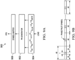
- FIG. 9A is a diagram of a phase pilot symbol (PPS) generator circuit 900 or 901 that may be used in FIGS. 8A , 8C , or 8D .
- the PPS generator includes a pseudorandom noise (PN) generator circuit 902 that may be formed from one or more linear feedback shift registers (LFSRs) with appropriate feedback circuitry.
- the PN generator circuit 902 preferably generates a pseudorandom noise (PN) sequence such as a Gold code that is used for the PPS symbols.
- the PPS generator includes a symbol mapper circuit 906 that is coupled to receive the PN sequence.
- the symbol mapper circuit 906 preferably maps two PN sequence bits into a quadrature phase shift keyed (QPSK) symbol to form a PPS.
- QPSK quadrature phase shift keyed
- the symbol mapper may be adapted to map PN sequence bits to other symbols, such as QAM symbols.
- the QPSK PPS is preferably produced at a higher power than the QAM data symbols to facilitate receiver phase noise mitigation under low SNR or bad channel conditions.
- the PPS generator also includes a seed circuit 904 that is coupled to receive a load signal. An active level of the load signal loads the initialization sequence c init into generator circuit 902 at the start of each radio frame.
- c init may be as defined by equation [1].
- n RU is the index of a remote unit (RU) or other receiving unit as in FIG. 1
- q is a binary codeword index
- i DL,UL is a binary index indicating a downlink (DL) or uplink (UL) sequence
- N is the cell ID of the wireless cell.
- the notation 2 K is used to indicate stage K of an LFSR which receives the initialization seed.
- FIG. 9B is a diagram showing phase pilot symbols inserted within 48 QAM symbols.
- the PPS is inserted into a Phase Pilot (PHP) block having a predetermined even length N PHP such as 48.
- N DFT / N PHP phase pilot symbols are inserted into the PHP block.
- each PPS is inserted such that N PHP /2-1 modulation symbols are before the PPS, and N PHP / 2 modulation symbols are after the PPS.
- the left PHP block of FIG. 9B includes 23 leading modulation symbols, one PPS, and 24 trailing modulation symbols for a total of 48 symbols.
- the PPS is inserted such that N PHP,last /2-1 modulation symbols are before the PPS, and N PHP,last /2 modulation symbols are after the PPS.
- the PPS advantageously compensates for phase noise embedded in the QAM symbol stream with only a 2% overhead. Insertion of the PPS is preferably enabled or disabled through higher layer signaling for each RU or receiving unit independently.
- Embodiments may be implemented in software, hardware, or a combination of both.
Landscapes
- Engineering & Computer Science (AREA)
- Computer Networks & Wireless Communication (AREA)
- Signal Processing (AREA)
- Physics & Mathematics (AREA)
- Discrete Mathematics (AREA)
- General Physics & Mathematics (AREA)
- Mathematical Physics (AREA)
- Mobile Radio Communication Systems (AREA)
- Transmitters (AREA)
Applications Claiming Priority (3)
| Application Number | Priority Date | Filing Date | Title |
|---|---|---|---|
| US201562107038P | 2015-01-23 | 2015-01-23 | |
| US14/971,624 US10454739B2 (en) | 2015-01-23 | 2015-12-16 | Transmission scheme for SC-FDMA with two DFT-precoding stages |
| PCT/US2016/014632 WO2016118929A2 (en) | 2015-01-23 | 2016-01-22 | Transmission scheme for sc-fdma with two dft-precoding stages |
Publications (3)
| Publication Number | Publication Date |
|---|---|
| EP3300548A2 EP3300548A2 (en) | 2018-04-04 |
| EP3300548A4 EP3300548A4 (en) | 2019-08-28 |
| EP3300548B1 true EP3300548B1 (en) | 2023-05-10 |
Family
ID=56417928
Family Applications (1)
| Application Number | Title | Priority Date | Filing Date |
|---|---|---|---|
| EP16740881.4A Active EP3300548B1 (en) | 2015-01-23 | 2016-01-22 | Transmission scheme for sc-fdma with two dft-precoding stages |
Country Status (5)
| Country | Link |
|---|---|
| US (2) | US10454739B2 (enExample) |
| EP (1) | EP3300548B1 (enExample) |
| JP (3) | JP2018511194A (enExample) |
| CN (2) | CN112866169A (enExample) |
| WO (1) | WO2016118929A2 (enExample) |
Families Citing this family (9)
| Publication number | Priority date | Publication date | Assignee | Title |
|---|---|---|---|---|
| US9246635B2 (en) * | 2013-11-11 | 2016-01-26 | Lg Electronics Inc. | Apparatus for transmitting broadcast signals, apparatus for receiving broadcast signals, method for transmitting broadcast signals and method for receiving broadcast signals |
| EP4513818A3 (en) | 2017-03-22 | 2025-04-30 | Mitsubishi Electric R&D Centre Europe B.V. | Reference signal for phase tracking insertion |
| US10700907B2 (en) | 2017-07-12 | 2020-06-30 | Qualcomm Incorporated | Waveform for millimeter wave new radio |
| US10841143B2 (en) * | 2017-12-12 | 2020-11-17 | Qualcomm Incorporated | Phase tracking reference signal for sub-symbol phase tracking |
| US11057261B2 (en) * | 2018-12-26 | 2021-07-06 | Cable Television Laboratories, Inc. | Systems and methods for transmitting data via an electrical cable |
| CN110602748B (zh) * | 2019-08-23 | 2022-11-29 | 北京紫光展锐通信技术有限公司 | 数据接收方法及装置、控制方法及装置 |
| CN115812295B (zh) * | 2020-07-17 | 2024-06-11 | 高通股份有限公司 | 6ghz频带的nr-u:跨分量载波(cc)传输的峰值平均功率比(papr)降低 |
| US11916702B2 (en) * | 2021-12-20 | 2024-02-27 | Qualcomm Incorporated | Tone reservation for digital post distortion |
| KR20250008492A (ko) * | 2023-07-07 | 2025-01-14 | 한국전자통신연구원 | 위상 왜곡에 면역력이 있는 신호 설계 방법 및 장치 |
Family Cites Families (55)
| Publication number | Priority date | Publication date | Assignee | Title |
|---|---|---|---|---|
| JPS54134917A (en) * | 1978-04-12 | 1979-10-19 | Kokusai Denshin Denwa Co Ltd | Device for reducing sampled frequency |
| US7684568B2 (en) * | 2003-11-24 | 2010-03-23 | Intellon Corporation | Encrypting data in a communication network |
| US8019006B2 (en) * | 2005-05-19 | 2011-09-13 | Samsung Electronics Co., Ltd. | Apparatus and method for FT pre-coding of data and control signals to reduce PAPR in a multi-carrier wireless network |
| KR101137329B1 (ko) * | 2005-06-15 | 2012-04-19 | 엘지전자 주식회사 | 다중 반송파 시스템에서의 부반송파 할당 방법 및 그 장치 |
| KR101306696B1 (ko) * | 2005-11-10 | 2013-09-10 | 엘지전자 주식회사 | 다수의 반송파를 이용하여 데이터를 전송하는 장치 및 방법 |
| CN101379748A (zh) * | 2006-02-10 | 2009-03-04 | 交互数字技术公司 | 在多输入多输出单载波频分多址系统中用于执行上行链路传输的方法和设备 |
| JP2007329588A (ja) | 2006-06-06 | 2007-12-20 | Fujitsu Ltd | 送信機及び送信方法 |
| US7916775B2 (en) * | 2006-06-16 | 2011-03-29 | Lg Electronics Inc. | Encoding uplink acknowledgments to downlink transmissions |
| KR100957311B1 (ko) * | 2006-08-11 | 2010-05-13 | 삼성전자주식회사 | 이동통신 시스템에서 상향링크의 스케쥴링 방법 및 장치 |
| EP2087610B1 (en) * | 2006-10-31 | 2015-09-09 | QUALCOMM Incorporated | Unified design and centralized scheduling for dynamic simo, su-mimo and mu-mimo operation for rl transmissions |
| EP1928115A1 (en) * | 2006-11-30 | 2008-06-04 | Nokia Siemens Networks Gmbh & Co. Kg | Adaptive modulation and coding in a SC-FDMA system |
| US8451915B2 (en) * | 2007-03-21 | 2013-05-28 | Samsung Electronics Co., Ltd. | Efficient uplink feedback in a wireless communication system |
| JP4728301B2 (ja) | 2007-08-14 | 2011-07-20 | 株式会社エヌ・ティ・ティ・ドコモ | ユーザ装置、送信方法、及び通信システム |
| US9712279B2 (en) * | 2007-10-04 | 2017-07-18 | Samsung Electronics Co., Ltd. | Method and apparatus for interleaving data in a mobile communication system |
| KR101613893B1 (ko) * | 2007-10-04 | 2016-04-20 | 삼성전자주식회사 | 이동통신 시스템에서 데이터 인터리빙 방법 및 장치 |
| US9363126B2 (en) * | 2007-12-21 | 2016-06-07 | Google Technology Holdings LLC | Method and apparatus for IFDMA receiver architecture |
| WO2009104679A1 (ja) * | 2008-02-20 | 2009-08-27 | シャープ株式会社 | 無線送信装置、無線受信装置、無線通信システムおよび無線送信方法 |
| US9225575B2 (en) * | 2008-06-18 | 2015-12-29 | Center Of Excellence In Wireless Technology | Precoding for single transmission streams in multiple antenna systems |
| KR101497154B1 (ko) * | 2008-06-26 | 2015-03-02 | 엘지전자 주식회사 | Sc-fdma 시스템에서 전송 다이버시티를 이용한 데이터 전송장치 및 방법 |
| KR101500754B1 (ko) * | 2008-08-04 | 2015-03-10 | 엘지전자 주식회사 | 다중 rf 시스템에서 데이터 전송 방법 |
| CN102106102A (zh) * | 2008-08-08 | 2011-06-22 | 夏普株式会社 | 无线通信系统、发送装置、接收装置 |
| KR101440628B1 (ko) * | 2008-08-11 | 2014-09-17 | 엘지전자 주식회사 | Sc-fdma 시스템에서 전송 다이버시티를 이용한 데이터 전송장치 및 방법 |
| KR20100019948A (ko) * | 2008-08-11 | 2010-02-19 | 엘지전자 주식회사 | 공간 다중화 기법을 이용한 데이터 전송방법 |
| US9369238B2 (en) * | 2008-08-12 | 2016-06-14 | Telefonaktiebolaget L M Ericsson (Publ) | Method and arrangement in a communication system |
| KR101549021B1 (ko) * | 2008-08-20 | 2015-09-01 | 엘지전자 주식회사 | 상향링크 papr을 줄이기 위한 프리코딩 방법 및 이를 위한 장치 |
| EP2327192B1 (en) * | 2008-09-19 | 2012-07-11 | Telefonaktiebolaget LM Ericsson (publ) | A transmitter stage and a corresponding method for transmitting signals on multiple frequency resources in a telecommunication system |
| CN102160310B (zh) * | 2008-09-22 | 2014-06-18 | 松下电器产业株式会社 | 无线通信装置及信号分割方法 |
| US8644397B2 (en) * | 2008-09-23 | 2014-02-04 | Qualcomm Incorporated | Efficient multiplexing of reference signal and data in a wireless communication system |
| US8406113B2 (en) * | 2008-10-17 | 2013-03-26 | Freescale Semiconductor, Inc. | Peak-to-average reduction of SC-FDMA signals with frequency mask |
| KR101652560B1 (ko) * | 2008-11-14 | 2016-08-30 | 파나소닉 인텔렉츄얼 프로퍼티 코포레이션 오브 아메리카 | 기지국 장치 및 리소스 할당 방법 |
| WO2010062230A1 (en) * | 2008-11-27 | 2010-06-03 | Telefonaktiebolaget L M Ericsson (Publ) | Methods and arrangements for peak to average power ratio reduction |
| CN104184595B (zh) * | 2009-04-01 | 2017-09-29 | 高通股份有限公司 | 管理通过共享通信介质通信的节点间的传输的装置 |
| EP2432135B1 (en) * | 2009-05-11 | 2018-02-21 | LG Electronics Inc. | Reference signal transmitting method and device in a multi-antenna system |
| JP2011097367A (ja) * | 2009-10-29 | 2011-05-12 | Sharp Corp | 送信装置、無線通信システム、移動局装置の制御プログラムおよび基地局装置の制御プログラム |
| CN102098141A (zh) * | 2009-12-10 | 2011-06-15 | 普天信息技术研究院有限公司 | Sc-fdma系统中链路传输装置及方法和空时块码编码器及方法 |
| KR101733489B1 (ko) * | 2010-01-17 | 2017-05-24 | 엘지전자 주식회사 | 무선 통신 시스템에서 제어 정보의 전송 방법 및 장치 |
| TR201810097T4 (tr) * | 2010-01-18 | 2018-08-27 | Ericsson Telefon Ab L M | Telsiz baz istasyonu ve kullanıcı aleti ve oradaki usuller. |
| KR101782647B1 (ko) * | 2010-01-28 | 2017-09-28 | 엘지전자 주식회사 | 무선 통신 시스템에서 상향링크 제어 정보 인코딩 방법 및 장치 |
| KR101802518B1 (ko) * | 2010-03-03 | 2017-11-29 | 엘지전자 주식회사 | 무선 통신 시스템에서 상향링크 제어 정보 전송 방법 및 장치 |
| US8839078B2 (en) * | 2010-03-05 | 2014-09-16 | Samsung Electronics Co., Ltd. | Application layer FEC framework for WiGig |
| US9025428B2 (en) * | 2010-04-14 | 2015-05-05 | Qualcomm Incorporated | Allocating and receiving tones for a frame |
| JP2011259108A (ja) * | 2010-06-07 | 2011-12-22 | Sharp Corp | 無線通信システム、送信装置および送信方法 |
| JP5486734B2 (ja) * | 2010-08-04 | 2014-05-07 | エヌイーシー(チャイナ)カンパニー, リミテッド | シングルキャリア通信システムにおける送信信号生成装置および方法 |
| WO2012176495A1 (ja) * | 2011-06-22 | 2012-12-27 | 三菱電機株式会社 | 送信装置、受信装置、通信システムおよび通信方法 |
| WO2013022272A2 (en) * | 2011-08-11 | 2013-02-14 | Lg Electronics Inc. | Apparatus for transmitting and receiving downlink control information in a wireless access system and method thereof |
| US9203672B2 (en) * | 2012-05-13 | 2015-12-01 | Broadcom Corporation | Multi-channel support within single user, multiple user, multiple access, and/or MIMO wireless communications |
| US9203673B2 (en) * | 2012-05-13 | 2015-12-01 | Broadcom Corporation | Multi-channel support within single user, multiple user, multiple access, and/or MIMO wireless communications |
| PL2920933T3 (pl) * | 2012-09-24 | 2018-09-28 | Nokia Solutions And Networks Oy | Korekcja błędu częstotliwości dla lte uplink comp |
| CN104685948A (zh) * | 2012-09-27 | 2015-06-03 | 夏普株式会社 | 终端、通信方法以及集成电路 |
| JP5951107B2 (ja) * | 2013-03-04 | 2016-07-13 | 三菱電機株式会社 | 送信装置、受信装置および通信システム |
| EP3793109A1 (en) * | 2013-03-13 | 2021-03-17 | Mitsubishi Electric Corporation | Transmission apparatus for suppressing out-of-band interferences |
| KR101895997B1 (ko) * | 2013-06-24 | 2018-09-06 | 한국전자통신연구원 | 주파수 분할 다중 접속을 위한 송신기 및 수신기 |
| WO2015005743A1 (ko) * | 2013-07-12 | 2015-01-15 | 엘지전자 주식회사 | 무선 통신 시스템에서 신호 송수신방법 및 장치 |
| US9253428B2 (en) * | 2014-05-21 | 2016-02-02 | Arthur Webb Allison, III | Broadcasting system with digital television signals and metadata that modulate respective sets of OFDM carriers |
| US9497056B2 (en) * | 2014-06-09 | 2016-11-15 | Allen LeRoy Limberg | Conveying metadata by modulation of pilot carriers in COFDM broadcasting |
-
2015
- 2015-12-16 US US14/971,624 patent/US10454739B2/en active Active
-
2016
- 2016-01-22 CN CN202110368328.9A patent/CN112866169A/zh active Pending
- 2016-01-22 EP EP16740881.4A patent/EP3300548B1/en active Active
- 2016-01-22 CN CN201680006733.3A patent/CN107912081B/zh active Active
- 2016-01-22 JP JP2017538965A patent/JP2018511194A/ja active Pending
- 2016-01-22 WO PCT/US2016/014632 patent/WO2016118929A2/en not_active Ceased
-
2019
- 2019-09-04 US US16/559,667 patent/US20200007376A1/en active Pending
-
2022
- 2022-09-09 JP JP2022143651A patent/JP2022172355A/ja active Pending
-
2024
- 2024-12-27 JP JP2024231947A patent/JP2025041953A/ja active Pending
Also Published As
| Publication number | Publication date |
|---|---|
| US20200007376A1 (en) | 2020-01-02 |
| EP3300548A4 (en) | 2019-08-28 |
| CN107912081B (zh) | 2021-04-06 |
| WO2016118929A3 (en) | 2018-02-22 |
| JP2022172355A (ja) | 2022-11-15 |
| JP2018511194A (ja) | 2018-04-19 |
| JP2025041953A (ja) | 2025-03-26 |
| US10454739B2 (en) | 2019-10-22 |
| CN107912081A (zh) | 2018-04-13 |
| CN112866169A (zh) | 2021-05-28 |
| US20160218905A1 (en) | 2016-07-28 |
| EP3300548A2 (en) | 2018-04-04 |
| WO2016118929A2 (en) | 2016-07-28 |
Similar Documents
| Publication | Publication Date | Title |
|---|---|---|
| EP3300548B1 (en) | Transmission scheme for sc-fdma with two dft-precoding stages | |
| US11108605B2 (en) | Phase tracking reference signal processing method and apparatus | |
| US10785769B2 (en) | Physical downlink control channel design for 5G new radio | |
| CN109565361B (zh) | 用于确定传输块大小的方法及无线装置 | |
| EP3146782B1 (en) | System and method for orthogonal frequency division multiple access | |
| US8743815B2 (en) | Method and base station for transmitting SA-preamble and method and user equipment for receiving SA-preamble | |
| EP3248424B1 (en) | High performance nlos wireless backhaul frame structure | |
| US8254247B2 (en) | Method and apparatus for transmitting signal in a wireless communication system | |
| EP4011162A1 (en) | Physical uplink control channel (pucch) and reference signal design for new radio-unlicensed (nr-u) | |
| US20110194514A1 (en) | Method and apparatus of receiving data in wireless communication system | |
| EP2590375A1 (en) | Uplink baseband signal compression method, decompression method, device, and system | |
| WO2012074273A2 (ko) | 무선 통신 시스템에서 상향링크 제어정보를 위한 자원 할당 방법 및 이를 위한 단말 | |
| KR20110073189A (ko) | 다중 안테나를 지원하는 무선 이동 통신 시스템에 있어서, 상향링크 데이터와 제어정보를 전송하는 방법 및 장치 | |
| US20130114477A1 (en) | Method for transmitting response information in a wireless communication system, and apparatus for same | |
| CN107409393A (zh) | 用于点到多点nlos无线回程的低开销信令 | |
| WO2025051397A2 (en) | Devices and methods for reliable communication in a wireless network |
Legal Events
| Date | Code | Title | Description |
|---|---|---|---|
| STAA | Information on the status of an ep patent application or granted ep patent |
Free format text: STATUS: THE INTERNATIONAL PUBLICATION HAS BEEN MADE |
|
| PUAI | Public reference made under article 153(3) epc to a published international application that has entered the european phase |
Free format text: ORIGINAL CODE: 0009012 |
|
| STAA | Information on the status of an ep patent application or granted ep patent |
Free format text: STATUS: THE APPLICATION HAS BEEN PUBLISHED |
|
| AK | Designated contracting states |
Kind code of ref document: A2 Designated state(s): AL AT BE BG CH CY CZ DE DK EE ES FI FR GB GR HR HU IE IS IT LI LT LU LV MC MK MT NL NO PL PT RO RS SE SI SK SM TR |
|
| AX | Request for extension of the european patent |
Extension state: BA ME |
|
| STAA | Information on the status of an ep patent application or granted ep patent |
Free format text: STATUS: REQUEST FOR EXAMINATION WAS MADE |
|
| 17P | Request for examination filed |
Effective date: 20180822 |
|
| RBV | Designated contracting states (corrected) |
Designated state(s): AL AT BE BG CH CY CZ DE DK EE ES FI FR GB GR HR HU IE IS IT LI LT LU LV MC MK MT NL NO PL PT RO RS SE SI SK SM TR |
|
| DAV | Request for validation of the european patent (deleted) | ||
| DAX | Request for extension of the european patent (deleted) | ||
| RIC1 | Information provided on ipc code assigned before grant |
Ipc: H04L 27/26 20060101AFI20190305BHEP Ipc: H04B 7/0456 20170101ALI20190305BHEP Ipc: H04L 1/00 20060101ALN20190305BHEP |
|
| A4 | Supplementary search report drawn up and despatched |
Effective date: 20190725 |
|
| RIC1 | Information provided on ipc code assigned before grant |
Ipc: H04L 27/26 20060101AFI20190719BHEP Ipc: H04L 1/00 20060101ALN20190719BHEP Ipc: H04B 7/0456 20170101ALI20190719BHEP |
|
| STAA | Information on the status of an ep patent application or granted ep patent |
Free format text: STATUS: EXAMINATION IS IN PROGRESS |
|
| 17Q | First examination report despatched |
Effective date: 20201021 |
|
| GRAP | Despatch of communication of intention to grant a patent |
Free format text: ORIGINAL CODE: EPIDOSNIGR1 |
|
| RIC1 | Information provided on ipc code assigned before grant |
Ipc: H04L 1/00 20060101ALN20221110BHEP Ipc: H04B 7/0456 20170101ALI20221110BHEP Ipc: H04L 27/26 20060101AFI20221110BHEP |
|
| STAA | Information on the status of an ep patent application or granted ep patent |
Free format text: STATUS: GRANT OF PATENT IS INTENDED |
|
| RIC1 | Information provided on ipc code assigned before grant |
Ipc: H04L 1/00 20060101ALN20221117BHEP Ipc: H04B 7/0456 20170101ALI20221117BHEP Ipc: H04L 27/26 20060101AFI20221117BHEP |
|
| RIC1 | Information provided on ipc code assigned before grant |
Ipc: H04L 1/00 20060101ALN20221124BHEP Ipc: H04B 7/0456 20170101ALI20221124BHEP Ipc: H04L 27/26 20060101AFI20221124BHEP |
|
| INTG | Intention to grant announced |
Effective date: 20221215 |
|
| GRAS | Grant fee paid |
Free format text: ORIGINAL CODE: EPIDOSNIGR3 |
|
| GRAA | (expected) grant |
Free format text: ORIGINAL CODE: 0009210 |
|
| STAA | Information on the status of an ep patent application or granted ep patent |
Free format text: STATUS: THE PATENT HAS BEEN GRANTED |
|
| AK | Designated contracting states |
Kind code of ref document: B1 Designated state(s): AL AT BE BG CH CY CZ DE DK EE ES FI FR GB GR HR HU IE IS IT LI LT LU LV MC MK MT NL NO PL PT RO RS SE SI SK SM TR |
|
| REG | Reference to a national code |
Ref country code: GB Ref legal event code: FG4D |
|
| REG | Reference to a national code |
Ref country code: AT Ref legal event code: REF Ref document number: 1567835 Country of ref document: AT Kind code of ref document: T Effective date: 20230515 Ref country code: CH Ref legal event code: EP |
|
| REG | Reference to a national code |
Ref country code: DE Ref legal event code: R096 Ref document number: 602016079325 Country of ref document: DE |
|
| REG | Reference to a national code |
Ref country code: IE Ref legal event code: FG4D |
|
| P01 | Opt-out of the competence of the unified patent court (upc) registered |
Effective date: 20230523 |
|
| REG | Reference to a national code |
Ref country code: LT Ref legal event code: MG9D |
|
| REG | Reference to a national code |
Ref country code: NL Ref legal event code: MP Effective date: 20230510 |
|
| REG | Reference to a national code |
Ref country code: AT Ref legal event code: MK05 Ref document number: 1567835 Country of ref document: AT Kind code of ref document: T Effective date: 20230510 |
|
| PG25 | Lapsed in a contracting state [announced via postgrant information from national office to epo] |
Ref country code: SE Free format text: LAPSE BECAUSE OF FAILURE TO SUBMIT A TRANSLATION OF THE DESCRIPTION OR TO PAY THE FEE WITHIN THE PRESCRIBED TIME-LIMIT Effective date: 20230510 Ref country code: PT Free format text: LAPSE BECAUSE OF FAILURE TO SUBMIT A TRANSLATION OF THE DESCRIPTION OR TO PAY THE FEE WITHIN THE PRESCRIBED TIME-LIMIT Effective date: 20230911 Ref country code: NO Free format text: LAPSE BECAUSE OF FAILURE TO SUBMIT A TRANSLATION OF THE DESCRIPTION OR TO PAY THE FEE WITHIN THE PRESCRIBED TIME-LIMIT Effective date: 20230810 Ref country code: NL Free format text: LAPSE BECAUSE OF FAILURE TO SUBMIT A TRANSLATION OF THE DESCRIPTION OR TO PAY THE FEE WITHIN THE PRESCRIBED TIME-LIMIT Effective date: 20230510 Ref country code: ES Free format text: LAPSE BECAUSE OF FAILURE TO SUBMIT A TRANSLATION OF THE DESCRIPTION OR TO PAY THE FEE WITHIN THE PRESCRIBED TIME-LIMIT Effective date: 20230510 Ref country code: AT Free format text: LAPSE BECAUSE OF FAILURE TO SUBMIT A TRANSLATION OF THE DESCRIPTION OR TO PAY THE FEE WITHIN THE PRESCRIBED TIME-LIMIT Effective date: 20230510 |
|
| PG25 | Lapsed in a contracting state [announced via postgrant information from national office to epo] |
Ref country code: RS Free format text: LAPSE BECAUSE OF FAILURE TO SUBMIT A TRANSLATION OF THE DESCRIPTION OR TO PAY THE FEE WITHIN THE PRESCRIBED TIME-LIMIT Effective date: 20230510 Ref country code: PL Free format text: LAPSE BECAUSE OF FAILURE TO SUBMIT A TRANSLATION OF THE DESCRIPTION OR TO PAY THE FEE WITHIN THE PRESCRIBED TIME-LIMIT Effective date: 20230510 Ref country code: LV Free format text: LAPSE BECAUSE OF FAILURE TO SUBMIT A TRANSLATION OF THE DESCRIPTION OR TO PAY THE FEE WITHIN THE PRESCRIBED TIME-LIMIT Effective date: 20230510 Ref country code: LT Free format text: LAPSE BECAUSE OF FAILURE TO SUBMIT A TRANSLATION OF THE DESCRIPTION OR TO PAY THE FEE WITHIN THE PRESCRIBED TIME-LIMIT Effective date: 20230510 Ref country code: IS Free format text: LAPSE BECAUSE OF FAILURE TO SUBMIT A TRANSLATION OF THE DESCRIPTION OR TO PAY THE FEE WITHIN THE PRESCRIBED TIME-LIMIT Effective date: 20230910 Ref country code: HR Free format text: LAPSE BECAUSE OF FAILURE TO SUBMIT A TRANSLATION OF THE DESCRIPTION OR TO PAY THE FEE WITHIN THE PRESCRIBED TIME-LIMIT Effective date: 20230510 Ref country code: GR Free format text: LAPSE BECAUSE OF FAILURE TO SUBMIT A TRANSLATION OF THE DESCRIPTION OR TO PAY THE FEE WITHIN THE PRESCRIBED TIME-LIMIT Effective date: 20230811 |
|
| PG25 | Lapsed in a contracting state [announced via postgrant information from national office to epo] |
Ref country code: FI Free format text: LAPSE BECAUSE OF FAILURE TO SUBMIT A TRANSLATION OF THE DESCRIPTION OR TO PAY THE FEE WITHIN THE PRESCRIBED TIME-LIMIT Effective date: 20230510 |
|
| PG25 | Lapsed in a contracting state [announced via postgrant information from national office to epo] |
Ref country code: SK Free format text: LAPSE BECAUSE OF FAILURE TO SUBMIT A TRANSLATION OF THE DESCRIPTION OR TO PAY THE FEE WITHIN THE PRESCRIBED TIME-LIMIT Effective date: 20230510 |
|
| PG25 | Lapsed in a contracting state [announced via postgrant information from national office to epo] |
Ref country code: SM Free format text: LAPSE BECAUSE OF FAILURE TO SUBMIT A TRANSLATION OF THE DESCRIPTION OR TO PAY THE FEE WITHIN THE PRESCRIBED TIME-LIMIT Effective date: 20230510 Ref country code: SK Free format text: LAPSE BECAUSE OF FAILURE TO SUBMIT A TRANSLATION OF THE DESCRIPTION OR TO PAY THE FEE WITHIN THE PRESCRIBED TIME-LIMIT Effective date: 20230510 Ref country code: RO Free format text: LAPSE BECAUSE OF FAILURE TO SUBMIT A TRANSLATION OF THE DESCRIPTION OR TO PAY THE FEE WITHIN THE PRESCRIBED TIME-LIMIT Effective date: 20230510 Ref country code: EE Free format text: LAPSE BECAUSE OF FAILURE TO SUBMIT A TRANSLATION OF THE DESCRIPTION OR TO PAY THE FEE WITHIN THE PRESCRIBED TIME-LIMIT Effective date: 20230510 Ref country code: DK Free format text: LAPSE BECAUSE OF FAILURE TO SUBMIT A TRANSLATION OF THE DESCRIPTION OR TO PAY THE FEE WITHIN THE PRESCRIBED TIME-LIMIT Effective date: 20230510 Ref country code: CZ Free format text: LAPSE BECAUSE OF FAILURE TO SUBMIT A TRANSLATION OF THE DESCRIPTION OR TO PAY THE FEE WITHIN THE PRESCRIBED TIME-LIMIT Effective date: 20230510 |
|
| REG | Reference to a national code |
Ref country code: DE Ref legal event code: R097 Ref document number: 602016079325 Country of ref document: DE |
|
| PLBE | No opposition filed within time limit |
Free format text: ORIGINAL CODE: 0009261 |
|
| STAA | Information on the status of an ep patent application or granted ep patent |
Free format text: STATUS: NO OPPOSITION FILED WITHIN TIME LIMIT |
|
| 26N | No opposition filed |
Effective date: 20240213 |
|
| PG25 | Lapsed in a contracting state [announced via postgrant information from national office to epo] |
Ref country code: SI Free format text: LAPSE BECAUSE OF FAILURE TO SUBMIT A TRANSLATION OF THE DESCRIPTION OR TO PAY THE FEE WITHIN THE PRESCRIBED TIME-LIMIT Effective date: 20230510 |
|
| PG25 | Lapsed in a contracting state [announced via postgrant information from national office to epo] |
Ref country code: SI Free format text: LAPSE BECAUSE OF FAILURE TO SUBMIT A TRANSLATION OF THE DESCRIPTION OR TO PAY THE FEE WITHIN THE PRESCRIBED TIME-LIMIT Effective date: 20230510 Ref country code: IT Free format text: LAPSE BECAUSE OF FAILURE TO SUBMIT A TRANSLATION OF THE DESCRIPTION OR TO PAY THE FEE WITHIN THE PRESCRIBED TIME-LIMIT Effective date: 20230510 |
|
| PG25 | Lapsed in a contracting state [announced via postgrant information from national office to epo] |
Ref country code: MC Free format text: LAPSE BECAUSE OF FAILURE TO SUBMIT A TRANSLATION OF THE DESCRIPTION OR TO PAY THE FEE WITHIN THE PRESCRIBED TIME-LIMIT Effective date: 20230510 |
|
| PG25 | Lapsed in a contracting state [announced via postgrant information from national office to epo] |
Ref country code: MC Free format text: LAPSE BECAUSE OF FAILURE TO SUBMIT A TRANSLATION OF THE DESCRIPTION OR TO PAY THE FEE WITHIN THE PRESCRIBED TIME-LIMIT Effective date: 20230510 |
|
| REG | Reference to a national code |
Ref country code: CH Ref legal event code: PL |
|
| PG25 | Lapsed in a contracting state [announced via postgrant information from national office to epo] |
Ref country code: LU Free format text: LAPSE BECAUSE OF NON-PAYMENT OF DUE FEES Effective date: 20240122 |
|
| PG25 | Lapsed in a contracting state [announced via postgrant information from national office to epo] |
Ref country code: LU Free format text: LAPSE BECAUSE OF NON-PAYMENT OF DUE FEES Effective date: 20240122 |
|
| PG25 | Lapsed in a contracting state [announced via postgrant information from national office to epo] |
Ref country code: BE Free format text: LAPSE BECAUSE OF NON-PAYMENT OF DUE FEES Effective date: 20240131 |
|
| PG25 | Lapsed in a contracting state [announced via postgrant information from national office to epo] |
Ref country code: CH Free format text: LAPSE BECAUSE OF NON-PAYMENT OF DUE FEES Effective date: 20240131 |
|
| PG25 | Lapsed in a contracting state [announced via postgrant information from national office to epo] |
Ref country code: CH Free format text: LAPSE BECAUSE OF NON-PAYMENT OF DUE FEES Effective date: 20240131 Ref country code: BE Free format text: LAPSE BECAUSE OF NON-PAYMENT OF DUE FEES Effective date: 20240131 |
|
| REG | Reference to a national code |
Ref country code: BE Ref legal event code: MM Effective date: 20240131 |
|
| PG25 | Lapsed in a contracting state [announced via postgrant information from national office to epo] |
Ref country code: BG Free format text: LAPSE BECAUSE OF FAILURE TO SUBMIT A TRANSLATION OF THE DESCRIPTION OR TO PAY THE FEE WITHIN THE PRESCRIBED TIME-LIMIT Effective date: 20230510 |
|
| PG25 | Lapsed in a contracting state [announced via postgrant information from national office to epo] |
Ref country code: BG Free format text: LAPSE BECAUSE OF FAILURE TO SUBMIT A TRANSLATION OF THE DESCRIPTION OR TO PAY THE FEE WITHIN THE PRESCRIBED TIME-LIMIT Effective date: 20230510 |
|
| PGFP | Annual fee paid to national office [announced via postgrant information from national office to epo] |
Ref country code: GB Payment date: 20241219 Year of fee payment: 10 |
|
| PGFP | Annual fee paid to national office [announced via postgrant information from national office to epo] |
Ref country code: FR Payment date: 20241219 Year of fee payment: 10 |
|
| PG25 | Lapsed in a contracting state [announced via postgrant information from national office to epo] |
Ref country code: IE Free format text: LAPSE BECAUSE OF NON-PAYMENT OF DUE FEES Effective date: 20240122 |
|
| PG25 | Lapsed in a contracting state [announced via postgrant information from national office to epo] |
Ref country code: IE Free format text: LAPSE BECAUSE OF NON-PAYMENT OF DUE FEES Effective date: 20240122 |
|
| PGFP | Annual fee paid to national office [announced via postgrant information from national office to epo] |
Ref country code: DE Payment date: 20241218 Year of fee payment: 10 |
|
| PG25 | Lapsed in a contracting state [announced via postgrant information from national office to epo] |
Ref country code: CY Free format text: LAPSE BECAUSE OF FAILURE TO SUBMIT A TRANSLATION OF THE DESCRIPTION OR TO PAY THE FEE WITHIN THE PRESCRIBED TIME-LIMIT; INVALID AB INITIO Effective date: 20160122 |
|
| PG25 | Lapsed in a contracting state [announced via postgrant information from national office to epo] |
Ref country code: HU Free format text: LAPSE BECAUSE OF FAILURE TO SUBMIT A TRANSLATION OF THE DESCRIPTION OR TO PAY THE FEE WITHIN THE PRESCRIBED TIME-LIMIT; INVALID AB INITIO Effective date: 20160122 |