EP3300068B1 - Anzeigevorrichtung mit organischen leuchtdioden - Google Patents
Anzeigevorrichtung mit organischen leuchtdioden Download PDFInfo
- Publication number
- EP3300068B1 EP3300068B1 EP17192771.8A EP17192771A EP3300068B1 EP 3300068 B1 EP3300068 B1 EP 3300068B1 EP 17192771 A EP17192771 A EP 17192771A EP 3300068 B1 EP3300068 B1 EP 3300068B1
- Authority
- EP
- European Patent Office
- Prior art keywords
- light
- gray level
- pixel
- induced deterioration
- image signal
- Prior art date
- Legal status (The legal status is an assumption and is not a legal conclusion. Google has not performed a legal analysis and makes no representation as to the accuracy of the status listed.)
- Active
Links
Images







Classifications
-
- G—PHYSICS
- G09—EDUCATION; CRYPTOGRAPHY; DISPLAY; ADVERTISING; SEALS
- G09G—ARRANGEMENTS OR CIRCUITS FOR CONTROL OF INDICATING DEVICES USING STATIC MEANS TO PRESENT VARIABLE INFORMATION
- G09G3/00—Control arrangements or circuits, of interest only in connection with visual indicators other than cathode-ray tubes
- G09G3/20—Control arrangements or circuits, of interest only in connection with visual indicators other than cathode-ray tubes for presentation of an assembly of a number of characters, e.g. a page, by composing the assembly by combination of individual elements arranged in a matrix no fixed position being assigned to or needed to be assigned to the individual characters or partial characters
- G09G3/22—Control arrangements or circuits, of interest only in connection with visual indicators other than cathode-ray tubes for presentation of an assembly of a number of characters, e.g. a page, by composing the assembly by combination of individual elements arranged in a matrix no fixed position being assigned to or needed to be assigned to the individual characters or partial characters using controlled light sources
- G09G3/30—Control arrangements or circuits, of interest only in connection with visual indicators other than cathode-ray tubes for presentation of an assembly of a number of characters, e.g. a page, by composing the assembly by combination of individual elements arranged in a matrix no fixed position being assigned to or needed to be assigned to the individual characters or partial characters using controlled light sources using electroluminescent panels
- G09G3/32—Control arrangements or circuits, of interest only in connection with visual indicators other than cathode-ray tubes for presentation of an assembly of a number of characters, e.g. a page, by composing the assembly by combination of individual elements arranged in a matrix no fixed position being assigned to or needed to be assigned to the individual characters or partial characters using controlled light sources using electroluminescent panels semiconductive, e.g. using light-emitting diodes [LED]
- G09G3/3208—Control arrangements or circuits, of interest only in connection with visual indicators other than cathode-ray tubes for presentation of an assembly of a number of characters, e.g. a page, by composing the assembly by combination of individual elements arranged in a matrix no fixed position being assigned to or needed to be assigned to the individual characters or partial characters using controlled light sources using electroluminescent panels semiconductive, e.g. using light-emitting diodes [LED] organic, e.g. using organic light-emitting diodes [OLED]
- G09G3/3275—Details of drivers for data electrodes
- G09G3/3291—Details of drivers for data electrodes in which the data driver supplies a variable data voltage for setting the current through, or the voltage across, the light-emitting elements
-
- G—PHYSICS
- G09—EDUCATION; CRYPTOGRAPHY; DISPLAY; ADVERTISING; SEALS
- G09G—ARRANGEMENTS OR CIRCUITS FOR CONTROL OF INDICATING DEVICES USING STATIC MEANS TO PRESENT VARIABLE INFORMATION
- G09G3/00—Control arrangements or circuits, of interest only in connection with visual indicators other than cathode-ray tubes
- G09G3/20—Control arrangements or circuits, of interest only in connection with visual indicators other than cathode-ray tubes for presentation of an assembly of a number of characters, e.g. a page, by composing the assembly by combination of individual elements arranged in a matrix no fixed position being assigned to or needed to be assigned to the individual characters or partial characters
- G09G3/2007—Display of intermediate tones
- G09G3/2018—Display of intermediate tones by time modulation using two or more time intervals
-
- G—PHYSICS
- G09—EDUCATION; CRYPTOGRAPHY; DISPLAY; ADVERTISING; SEALS
- G09G—ARRANGEMENTS OR CIRCUITS FOR CONTROL OF INDICATING DEVICES USING STATIC MEANS TO PRESENT VARIABLE INFORMATION
- G09G3/00—Control arrangements or circuits, of interest only in connection with visual indicators other than cathode-ray tubes
- G09G3/20—Control arrangements or circuits, of interest only in connection with visual indicators other than cathode-ray tubes for presentation of an assembly of a number of characters, e.g. a page, by composing the assembly by combination of individual elements arranged in a matrix no fixed position being assigned to or needed to be assigned to the individual characters or partial characters
- G09G3/22—Control arrangements or circuits, of interest only in connection with visual indicators other than cathode-ray tubes for presentation of an assembly of a number of characters, e.g. a page, by composing the assembly by combination of individual elements arranged in a matrix no fixed position being assigned to or needed to be assigned to the individual characters or partial characters using controlled light sources
- G09G3/30—Control arrangements or circuits, of interest only in connection with visual indicators other than cathode-ray tubes for presentation of an assembly of a number of characters, e.g. a page, by composing the assembly by combination of individual elements arranged in a matrix no fixed position being assigned to or needed to be assigned to the individual characters or partial characters using controlled light sources using electroluminescent panels
- G09G3/32—Control arrangements or circuits, of interest only in connection with visual indicators other than cathode-ray tubes for presentation of an assembly of a number of characters, e.g. a page, by composing the assembly by combination of individual elements arranged in a matrix no fixed position being assigned to or needed to be assigned to the individual characters or partial characters using controlled light sources using electroluminescent panels semiconductive, e.g. using light-emitting diodes [LED]
- G09G3/3208—Control arrangements or circuits, of interest only in connection with visual indicators other than cathode-ray tubes for presentation of an assembly of a number of characters, e.g. a page, by composing the assembly by combination of individual elements arranged in a matrix no fixed position being assigned to or needed to be assigned to the individual characters or partial characters using controlled light sources using electroluminescent panels semiconductive, e.g. using light-emitting diodes [LED] organic, e.g. using organic light-emitting diodes [OLED]
- G09G3/3225—Control arrangements or circuits, of interest only in connection with visual indicators other than cathode-ray tubes for presentation of an assembly of a number of characters, e.g. a page, by composing the assembly by combination of individual elements arranged in a matrix no fixed position being assigned to or needed to be assigned to the individual characters or partial characters using controlled light sources using electroluminescent panels semiconductive, e.g. using light-emitting diodes [LED] organic, e.g. using organic light-emitting diodes [OLED] using an active matrix
-
- G—PHYSICS
- G09—EDUCATION; CRYPTOGRAPHY; DISPLAY; ADVERTISING; SEALS
- G09G—ARRANGEMENTS OR CIRCUITS FOR CONTROL OF INDICATING DEVICES USING STATIC MEANS TO PRESENT VARIABLE INFORMATION
- G09G3/00—Control arrangements or circuits, of interest only in connection with visual indicators other than cathode-ray tubes
- G09G3/20—Control arrangements or circuits, of interest only in connection with visual indicators other than cathode-ray tubes for presentation of an assembly of a number of characters, e.g. a page, by composing the assembly by combination of individual elements arranged in a matrix no fixed position being assigned to or needed to be assigned to the individual characters or partial characters
- G09G3/22—Control arrangements or circuits, of interest only in connection with visual indicators other than cathode-ray tubes for presentation of an assembly of a number of characters, e.g. a page, by composing the assembly by combination of individual elements arranged in a matrix no fixed position being assigned to or needed to be assigned to the individual characters or partial characters using controlled light sources
- G09G3/30—Control arrangements or circuits, of interest only in connection with visual indicators other than cathode-ray tubes for presentation of an assembly of a number of characters, e.g. a page, by composing the assembly by combination of individual elements arranged in a matrix no fixed position being assigned to or needed to be assigned to the individual characters or partial characters using controlled light sources using electroluminescent panels
- G09G3/32—Control arrangements or circuits, of interest only in connection with visual indicators other than cathode-ray tubes for presentation of an assembly of a number of characters, e.g. a page, by composing the assembly by combination of individual elements arranged in a matrix no fixed position being assigned to or needed to be assigned to the individual characters or partial characters using controlled light sources using electroluminescent panels semiconductive, e.g. using light-emitting diodes [LED]
- G09G3/3208—Control arrangements or circuits, of interest only in connection with visual indicators other than cathode-ray tubes for presentation of an assembly of a number of characters, e.g. a page, by composing the assembly by combination of individual elements arranged in a matrix no fixed position being assigned to or needed to be assigned to the individual characters or partial characters using controlled light sources using electroluminescent panels semiconductive, e.g. using light-emitting diodes [LED] organic, e.g. using organic light-emitting diodes [OLED]
- G09G3/3225—Control arrangements or circuits, of interest only in connection with visual indicators other than cathode-ray tubes for presentation of an assembly of a number of characters, e.g. a page, by composing the assembly by combination of individual elements arranged in a matrix no fixed position being assigned to or needed to be assigned to the individual characters or partial characters using controlled light sources using electroluminescent panels semiconductive, e.g. using light-emitting diodes [LED] organic, e.g. using organic light-emitting diodes [OLED] using an active matrix
- G09G3/3233—Control arrangements or circuits, of interest only in connection with visual indicators other than cathode-ray tubes for presentation of an assembly of a number of characters, e.g. a page, by composing the assembly by combination of individual elements arranged in a matrix no fixed position being assigned to or needed to be assigned to the individual characters or partial characters using controlled light sources using electroluminescent panels semiconductive, e.g. using light-emitting diodes [LED] organic, e.g. using organic light-emitting diodes [OLED] using an active matrix with pixel circuitry controlling the current through the light-emitting element
-
- G—PHYSICS
- G09—EDUCATION; CRYPTOGRAPHY; DISPLAY; ADVERTISING; SEALS
- G09G—ARRANGEMENTS OR CIRCUITS FOR CONTROL OF INDICATING DEVICES USING STATIC MEANS TO PRESENT VARIABLE INFORMATION
- G09G3/00—Control arrangements or circuits, of interest only in connection with visual indicators other than cathode-ray tubes
- G09G3/20—Control arrangements or circuits, of interest only in connection with visual indicators other than cathode-ray tubes for presentation of an assembly of a number of characters, e.g. a page, by composing the assembly by combination of individual elements arranged in a matrix no fixed position being assigned to or needed to be assigned to the individual characters or partial characters
- G09G3/22—Control arrangements or circuits, of interest only in connection with visual indicators other than cathode-ray tubes for presentation of an assembly of a number of characters, e.g. a page, by composing the assembly by combination of individual elements arranged in a matrix no fixed position being assigned to or needed to be assigned to the individual characters or partial characters using controlled light sources
- G09G3/30—Control arrangements or circuits, of interest only in connection with visual indicators other than cathode-ray tubes for presentation of an assembly of a number of characters, e.g. a page, by composing the assembly by combination of individual elements arranged in a matrix no fixed position being assigned to or needed to be assigned to the individual characters or partial characters using controlled light sources using electroluminescent panels
- G09G3/32—Control arrangements or circuits, of interest only in connection with visual indicators other than cathode-ray tubes for presentation of an assembly of a number of characters, e.g. a page, by composing the assembly by combination of individual elements arranged in a matrix no fixed position being assigned to or needed to be assigned to the individual characters or partial characters using controlled light sources using electroluminescent panels semiconductive, e.g. using light-emitting diodes [LED]
- G09G3/3208—Control arrangements or circuits, of interest only in connection with visual indicators other than cathode-ray tubes for presentation of an assembly of a number of characters, e.g. a page, by composing the assembly by combination of individual elements arranged in a matrix no fixed position being assigned to or needed to be assigned to the individual characters or partial characters using controlled light sources using electroluminescent panels semiconductive, e.g. using light-emitting diodes [LED] organic, e.g. using organic light-emitting diodes [OLED]
- G09G3/3225—Control arrangements or circuits, of interest only in connection with visual indicators other than cathode-ray tubes for presentation of an assembly of a number of characters, e.g. a page, by composing the assembly by combination of individual elements arranged in a matrix no fixed position being assigned to or needed to be assigned to the individual characters or partial characters using controlled light sources using electroluminescent panels semiconductive, e.g. using light-emitting diodes [LED] organic, e.g. using organic light-emitting diodes [OLED] using an active matrix
- G09G3/3258—Control arrangements or circuits, of interest only in connection with visual indicators other than cathode-ray tubes for presentation of an assembly of a number of characters, e.g. a page, by composing the assembly by combination of individual elements arranged in a matrix no fixed position being assigned to or needed to be assigned to the individual characters or partial characters using controlled light sources using electroluminescent panels semiconductive, e.g. using light-emitting diodes [LED] organic, e.g. using organic light-emitting diodes [OLED] using an active matrix with pixel circuitry controlling the voltage across the light-emitting element
-
- G—PHYSICS
- G09—EDUCATION; CRYPTOGRAPHY; DISPLAY; ADVERTISING; SEALS
- G09G—ARRANGEMENTS OR CIRCUITS FOR CONTROL OF INDICATING DEVICES USING STATIC MEANS TO PRESENT VARIABLE INFORMATION
- G09G3/00—Control arrangements or circuits, of interest only in connection with visual indicators other than cathode-ray tubes
- G09G3/20—Control arrangements or circuits, of interest only in connection with visual indicators other than cathode-ray tubes for presentation of an assembly of a number of characters, e.g. a page, by composing the assembly by combination of individual elements arranged in a matrix no fixed position being assigned to or needed to be assigned to the individual characters or partial characters
- G09G3/22—Control arrangements or circuits, of interest only in connection with visual indicators other than cathode-ray tubes for presentation of an assembly of a number of characters, e.g. a page, by composing the assembly by combination of individual elements arranged in a matrix no fixed position being assigned to or needed to be assigned to the individual characters or partial characters using controlled light sources
- G09G3/30—Control arrangements or circuits, of interest only in connection with visual indicators other than cathode-ray tubes for presentation of an assembly of a number of characters, e.g. a page, by composing the assembly by combination of individual elements arranged in a matrix no fixed position being assigned to or needed to be assigned to the individual characters or partial characters using controlled light sources using electroluminescent panels
- G09G3/32—Control arrangements or circuits, of interest only in connection with visual indicators other than cathode-ray tubes for presentation of an assembly of a number of characters, e.g. a page, by composing the assembly by combination of individual elements arranged in a matrix no fixed position being assigned to or needed to be assigned to the individual characters or partial characters using controlled light sources using electroluminescent panels semiconductive, e.g. using light-emitting diodes [LED]
- G09G3/3208—Control arrangements or circuits, of interest only in connection with visual indicators other than cathode-ray tubes for presentation of an assembly of a number of characters, e.g. a page, by composing the assembly by combination of individual elements arranged in a matrix no fixed position being assigned to or needed to be assigned to the individual characters or partial characters using controlled light sources using electroluminescent panels semiconductive, e.g. using light-emitting diodes [LED] organic, e.g. using organic light-emitting diodes [OLED]
- G09G3/3275—Details of drivers for data electrodes
-
- G—PHYSICS
- G09—EDUCATION; CRYPTOGRAPHY; DISPLAY; ADVERTISING; SEALS
- G09G—ARRANGEMENTS OR CIRCUITS FOR CONTROL OF INDICATING DEVICES USING STATIC MEANS TO PRESENT VARIABLE INFORMATION
- G09G2300/00—Aspects of the constitution of display devices
- G09G2300/04—Structural and physical details of display devices
- G09G2300/0421—Structural details of the set of electrodes
- G09G2300/0426—Layout of electrodes and connections
-
- G—PHYSICS
- G09—EDUCATION; CRYPTOGRAPHY; DISPLAY; ADVERTISING; SEALS
- G09G—ARRANGEMENTS OR CIRCUITS FOR CONTROL OF INDICATING DEVICES USING STATIC MEANS TO PRESENT VARIABLE INFORMATION
- G09G2300/00—Aspects of the constitution of display devices
- G09G2300/04—Structural and physical details of display devices
- G09G2300/0439—Pixel structures
- G09G2300/0452—Details of colour pixel setup, e.g. pixel composed of a red, a blue and two green components
-
- G—PHYSICS
- G09—EDUCATION; CRYPTOGRAPHY; DISPLAY; ADVERTISING; SEALS
- G09G—ARRANGEMENTS OR CIRCUITS FOR CONTROL OF INDICATING DEVICES USING STATIC MEANS TO PRESENT VARIABLE INFORMATION
- G09G2310/00—Command of the display device
- G09G2310/08—Details of timing specific for flat panels, other than clock recovery
-
- G—PHYSICS
- G09—EDUCATION; CRYPTOGRAPHY; DISPLAY; ADVERTISING; SEALS
- G09G—ARRANGEMENTS OR CIRCUITS FOR CONTROL OF INDICATING DEVICES USING STATIC MEANS TO PRESENT VARIABLE INFORMATION
- G09G2320/00—Control of display operating conditions
- G09G2320/02—Improving the quality of display appearance
- G09G2320/0209—Crosstalk reduction, i.e. to reduce direct or indirect influences of signals directed to a certain pixel of the displayed image on other pixels of said image, inclusive of influences affecting pixels in different frames or fields or sub-images which constitute a same image, e.g. left and right images of a stereoscopic display
-
- G—PHYSICS
- G09—EDUCATION; CRYPTOGRAPHY; DISPLAY; ADVERTISING; SEALS
- G09G—ARRANGEMENTS OR CIRCUITS FOR CONTROL OF INDICATING DEVICES USING STATIC MEANS TO PRESENT VARIABLE INFORMATION
- G09G2320/00—Control of display operating conditions
- G09G2320/02—Improving the quality of display appearance
- G09G2320/0233—Improving the luminance or brightness uniformity across the screen
-
- G—PHYSICS
- G09—EDUCATION; CRYPTOGRAPHY; DISPLAY; ADVERTISING; SEALS
- G09G—ARRANGEMENTS OR CIRCUITS FOR CONTROL OF INDICATING DEVICES USING STATIC MEANS TO PRESENT VARIABLE INFORMATION
- G09G2320/00—Control of display operating conditions
- G09G2320/02—Improving the quality of display appearance
- G09G2320/0238—Improving the black level
-
- G—PHYSICS
- G09—EDUCATION; CRYPTOGRAPHY; DISPLAY; ADVERTISING; SEALS
- G09G—ARRANGEMENTS OR CIRCUITS FOR CONTROL OF INDICATING DEVICES USING STATIC MEANS TO PRESENT VARIABLE INFORMATION
- G09G2320/00—Control of display operating conditions
- G09G2320/02—Improving the quality of display appearance
- G09G2320/0285—Improving the quality of display appearance using tables for spatial correction of display data
-
- G—PHYSICS
- G09—EDUCATION; CRYPTOGRAPHY; DISPLAY; ADVERTISING; SEALS
- G09G—ARRANGEMENTS OR CIRCUITS FOR CONTROL OF INDICATING DEVICES USING STATIC MEANS TO PRESENT VARIABLE INFORMATION
- G09G2320/00—Control of display operating conditions
- G09G2320/04—Maintaining the quality of display appearance
-
- G—PHYSICS
- G09—EDUCATION; CRYPTOGRAPHY; DISPLAY; ADVERTISING; SEALS
- G09G—ARRANGEMENTS OR CIRCUITS FOR CONTROL OF INDICATING DEVICES USING STATIC MEANS TO PRESENT VARIABLE INFORMATION
- G09G2320/00—Control of display operating conditions
- G09G2320/04—Maintaining the quality of display appearance
- G09G2320/043—Preventing or counteracting the effects of ageing
-
- G—PHYSICS
- G09—EDUCATION; CRYPTOGRAPHY; DISPLAY; ADVERTISING; SEALS
- G09G—ARRANGEMENTS OR CIRCUITS FOR CONTROL OF INDICATING DEVICES USING STATIC MEANS TO PRESENT VARIABLE INFORMATION
- G09G2320/00—Control of display operating conditions
- G09G2320/04—Maintaining the quality of display appearance
- G09G2320/043—Preventing or counteracting the effects of ageing
- G09G2320/045—Compensation of drifts in the characteristics of light emitting or modulating elements
-
- G—PHYSICS
- G09—EDUCATION; CRYPTOGRAPHY; DISPLAY; ADVERTISING; SEALS
- G09G—ARRANGEMENTS OR CIRCUITS FOR CONTROL OF INDICATING DEVICES USING STATIC MEANS TO PRESENT VARIABLE INFORMATION
- G09G2320/00—Control of display operating conditions
- G09G2320/06—Adjustment of display parameters
- G09G2320/0693—Calibration of display systems
-
- G—PHYSICS
- G09—EDUCATION; CRYPTOGRAPHY; DISPLAY; ADVERTISING; SEALS
- G09G—ARRANGEMENTS OR CIRCUITS FOR CONTROL OF INDICATING DEVICES USING STATIC MEANS TO PRESENT VARIABLE INFORMATION
- G09G2320/00—Control of display operating conditions
- G09G2320/10—Special adaptations of display systems for operation with variable images
- G09G2320/103—Detection of image changes, e.g. determination of an index representative of the image change
-
- G—PHYSICS
- G09—EDUCATION; CRYPTOGRAPHY; DISPLAY; ADVERTISING; SEALS
- G09G—ARRANGEMENTS OR CIRCUITS FOR CONTROL OF INDICATING DEVICES USING STATIC MEANS TO PRESENT VARIABLE INFORMATION
- G09G3/00—Control arrangements or circuits, of interest only in connection with visual indicators other than cathode-ray tubes
- G09G3/20—Control arrangements or circuits, of interest only in connection with visual indicators other than cathode-ray tubes for presentation of an assembly of a number of characters, e.g. a page, by composing the assembly by combination of individual elements arranged in a matrix no fixed position being assigned to or needed to be assigned to the individual characters or partial characters
- G09G3/22—Control arrangements or circuits, of interest only in connection with visual indicators other than cathode-ray tubes for presentation of an assembly of a number of characters, e.g. a page, by composing the assembly by combination of individual elements arranged in a matrix no fixed position being assigned to or needed to be assigned to the individual characters or partial characters using controlled light sources
- G09G3/30—Control arrangements or circuits, of interest only in connection with visual indicators other than cathode-ray tubes for presentation of an assembly of a number of characters, e.g. a page, by composing the assembly by combination of individual elements arranged in a matrix no fixed position being assigned to or needed to be assigned to the individual characters or partial characters using controlled light sources using electroluminescent panels
- G09G3/32—Control arrangements or circuits, of interest only in connection with visual indicators other than cathode-ray tubes for presentation of an assembly of a number of characters, e.g. a page, by composing the assembly by combination of individual elements arranged in a matrix no fixed position being assigned to or needed to be assigned to the individual characters or partial characters using controlled light sources using electroluminescent panels semiconductive, e.g. using light-emitting diodes [LED]
- G09G3/3208—Control arrangements or circuits, of interest only in connection with visual indicators other than cathode-ray tubes for presentation of an assembly of a number of characters, e.g. a page, by composing the assembly by combination of individual elements arranged in a matrix no fixed position being assigned to or needed to be assigned to the individual characters or partial characters using controlled light sources using electroluminescent panels semiconductive, e.g. using light-emitting diodes [LED] organic, e.g. using organic light-emitting diodes [OLED]
- G09G3/3266—Details of drivers for scan electrodes
Definitions
- Embodiments of the present invention relate to a display device, and more particularly, to an organic light emitting diode (“OLED”) display device and a method of driving the OLED display device.
- OLED organic light emitting diode
- Display devices generally include a plurality of pixels provided in an area defined by a black matrix and/or a pixel defining layer. Examples of display devices may include a liquid crystal display (“LCD”) device, a plasma display panel (“PDP”) device, and an organic light emitting diode (“OLED”) display device.
- LCD liquid crystal display
- PDP plasma display panel
- OLED organic light emitting diode
- an OLED display device includes an insulating substrate, a thin film transistor ("TFT") disposed on the insulating substrate, a pixel electrode connected to the TFT, a partition wall dividing the pixel electrode, an organic layer disposed on the pixel electrode between the partition walls, and a common electrode disposed on the partition wall and the organic layer.
- TFT thin film transistor
- the TFT controls light emission of the organic layer for each pixel area.
- a pixel electrode is disposed in each pixel area, and each pixel electrode is electrically isolated from an adjacent pixel electrode so that each pixel electrode may be independently driven.
- the partition walls that divide the pixel areas are formed to be higher than the pixel electrodes. The partition walls serve to divide pixel areas while substantially preventing a short circuit between the pixel electrodes.
- An organic layer including a hole injection layer and an organic light emitting layer is formed on the pixel electrode between the partition walls.
- An OLED having such a structure controls light emitted from the organic light emitting layer to display an image.
- the lost light propagates inside the pixels and the peripheral pixels, thereby contributing to a deterioration of a TFT in the pixel.
- US 2007/0109284 A1 discloses a display device which can reduce the difference in deterioration of a display element in each pixel and suppress variations in light emission of a display element in a pixel.
- a gray scale of a display pattern is changed to prevent the difference in deterioration of display element in pixels from increasing.
- a specific display pattern is prevented from being fixedly displayed in a specific region.
- a pixel lagging behind in deterioration is deteriorated so that the accumulated lighting time of pixels is equal to each other.
- US 2011/0043551 A1 discloses an image processing apparatus that performs display control of an image displayed on a display unit, and includes a first control circuit for controlling image data of a frame in question or a display timing control signal corresponding to the image data so as to display each pixel forming the image with different brightness at given intervals, and a second control circuit for controlling the image data or the display timing control signal by different control from that by the first control circuit so as to display each pixel forming the image with different brightness at given intervals, wherein the first control circuit and the second control circuit control image data of an identical frame or a display timing control signal corresponding to the image data.
- An organic light emitting diode (OLED) display device has the features of Claim 1. Optional features of this aspect of the invention are set-out in Claims 2 to 9.
- a method of compensating for light-induced deterioration of an organic light emitting diode (OLED) display device has the features of Claim 10.
- Optional features of this aspect of the inmvention are set-out in Claims 11 to 13.
- FIG. 1 is an equivalent circuit diagram illustrating one pixel of an active matrix type organic light emitting diode (“AMOLED”) display device in accordance with an embodiment of the present invention.
- AMOLED active matrix type organic light emitting diode
- a pixel of the OLED display device includes a gate line G and a data line D, and further includes a switching transistor N1, a capacitor C, a driving transistor N2, and an organic light emitting diode (“OLED”) disposed between the gate line G and the data line D.
- each of the switching transistor N1 and the driving transistor N2 may be a thin film transistor (“TFT") including amorphous silicon (a-Si: H) or a TFT including an oxide based on a metal such as indium (In), gallium (Ga), zinc (Zn), tin (Sn) and/or titanium (Ti).
- a gate electrode of the switching transistor N1 is connected to the gate line G and a source electrode of the switching transistor N1 is connected to the data line D.
- One side of the capacitor C is connected to a drain electrode of the switching transistor N1 and another side of the capacitor C is grounded (GND) like a source electrode of the driving transistor N2.
- a drain electrode of the driving transistor N2 is connected to a cathode electrode of the OLED to which a driving voltage VDD is applied.
- a gate electrode of the driving transistor N2 is connected to the drain electrode of the switching transistor N1.
- the source electrode of the driving transistor N2 is grounded (GND).
- the switching transistor N1 is turned on in response to a gate signal applied from the gate line G to allow a current to flow between the source electrode and the drain electrode of the switching transistor N1.
- a data signal voltage, applied from the data line D during a turn-on period of the switching transistor N1, is applied to the gate electrode of the driving transistor N2 and the capacitor C via the source electrode and the drain electrode of the switching transistor N1.
- the driving transistor N2 controls a current flowing through the OLED according to the data signal voltage applied to the gate electrode of the driving transistor N2. Further, the capacitor C stores the data signal voltage and then maintains the data signal voltage at a constant level for one frame period of the OLED display device.
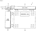
- FIG. 2 is a circuit diagram illustrating a comparative display device.
- the OLED display device 1 may include an OLED display panel 10, a gate driver 20, a data driver 30, and a timing controller 40.
- a plurality of gate lines G1 to Gn and a plurality of data lines D1 to Dm are formed in the OLED display panel.
- the gate lines G1 to Gn and the data lines D1 to Dm intersect one another and define pixel areas.
- the switching transistor N1, the driving transistor N2, the capacitor C and the OLED may be disposed in each pixel area P.
- a red pixel R, a green pixel G and a blue pixel B may be disposed in the pixel area of the OLED display panel 10.
- the pixels may be arranged in the form of a checkerboard or a stripe pattern.
- the gate driver 20 may generate a gate signal based on a gate control signal CNT1 applied from the timing controller 40 and may sequentially apply the gate signal to the plurality of gate lines G1 to Gn of the OLED display panel 10.
- the data driver 30 may generate a data signal voltage based on a data control signal CNT2 and an image data R', G' and B' applied from the timing controller 40 and may apply the data signal voltage to the plurality of data lines D1 to Dm of the OLED display panel 10.
- the timing controller 40 may generate the gate control signal CNT1 and the data control signal CNT2 for controlling the gate driver 20 and the data driver 30, respectively, based on a control signal CNT applied thereto, e.g., a vertical synchronization signal, a horizontal synchronization signal, a clock signal and a data enable signal.
- the gate control signal CNT1 and the data control signal CNT2 may be output to the gate driver 20 and the data driver 30, respectively.
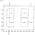
- FIG. 3 is a light-induced deterioration experimental image of a comparative OLED display panel.
- a screen area of the OLED display panel 10 illustrated in FIG. 3 corresponds to a horizontal line 0 to a horizontal line 600 in direction H, and corresponds to a vertical line 600 to a vertical line 1600 in direction V.
- An experimental image includes two red box images in an upper portion of the screen and two green box images located adjacent to and below the two red box images, respectively.
- a peripheral area in which the red box image and the green box image are not displayed is located within a non-light emitting state.
- a red pixel (hereinafter, "a pixel R”) emits light of a gray level 255, e.g. a maximum brightness.
- a green pixel (hereinafter, “a pixel G”) and a blue pixel (hereinafter, “a pixel B”) do not emit light, and have a gray level 0, e.g. a minimum brightness.
- a pixel G emits light of a gray level 255
- a pixel R and a pixel B do not emit light, having a gray level 0.
- the experimental image is input to the OLED display panel 10 as a fixed image without variation (e.g. a still image).
- FIG. 4 illustrates a resultant data image after displaying the experimental image of FIG. 3 .
- an upper portion of the screen in which the red box image is displayed for 5 hours is represented in light gray, and a voltage Vth of a pixel R has a value of about -0.3 V.
- a lower portion of the screen in which the green box image is displayed is represented in dark gray, and a voltage Vth of a pixel R has a value of about -0.4 V or less.
- a peripheral area around the red box image and the green box image in which light has not been emitted for 5 hours is represented in gray, and a voltage Vth of a pixel R in the peripheral area has a value in a range of about -0.25 V to about -0.35 V.
- the voltage Vth of the pixel R in the peripheral area is relatively low in pixels located closer to the red box image and the green box image, and relatively high in pixels spaced farther from the red box image and the green box image.
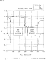
- FIG. 5 is a graph illustrating a voltage Vth from the experimental result of FIG. 3 .
- the graph in FIG. 5 illustrates a voltage Vth of a pixel R located at line A-A' illustrated in FIG. 3 .
- the horizontal axis of the graph represents a position of the pixel R in the OLED display panel, and the vertical axis represents a voltage Vth of the pixel R.
- the voltage Vth of the pixel R varies depending on the position.
- the pixel R maintains the voltage Vth in a range of about -0.3 V to about - 0.32 V, while in an area from a horizontal line 291 to a horizontal line 510 in which the green box image is displayed, the voltage Vth of the pixel R drops to about -0.48 V.
- the voltage Vth of the pixel R varies by about 0.16 V depending on the difference in the experimental image. The difference in the voltage Vth of the pixel R may further increase as the continuous light emission time of the experimental image increases.
- the voltage Vth of the pixel R does not experience a great change with the lapse of the light emission time.
- the voltage Vth of the pixel R is in a range of about -0.8333 V to about -0.787 V.
- a voltage Vth of the pixel R changes largely in accordance with a light emission time.
- a voltage Vth of a pixel R in a reference line 800 varies by about 0.5 V depending on whether the pixel R emits light.
- the graph of FIG. 5 shows that the voltage Vth of the pixel R is affected by whether the pixel R is turned on and by whether the adjacent pixel (e.g., the pixel G or the pixel B) is turned on and a light emission time of the adjacent pixel.
- a voltage Vth of one pixel that does not emit light may be significantly lowered in the case where another pixel in a peripheral area emits light for a long period of time.
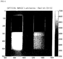
- FIG. 6 is an image illustrating an OLED display panel according to the experiment of FIG.4 .
- FIG. 6 is an image pictured when a pixel R of an OLED display panel emits light with a data signal voltage of a gray level 31 (31G) after the red pixel image and the green box image are continuously displayed for 5 hours as in FIG. 4 .
- a voltage Vth of a pixel R in an area where the red box image is displayed is about -0.32 V.
- a voltage Vth of a pixel R in an area where the green box image is displayed is about -0.48 V, which is lower than the voltage Vth of the pixel R in the area where the red box image is displayed.
- a driving voltage of the pixel R in the area where the green box image is displayed is higher than a driving voltage of the pixel R in the area where the red box image is displayed by about 0.16 V due to the effect of light-induced deterioration.
- a driving voltage applied to a light emitting layer of the pixel R is determined based on a difference between the data signal voltage and a voltage Vth of a driving transistor in the pixel R.
- the driving voltage of the pixel increases, and thus light may be emitted with a higher luminance than an applied gray value. Due to a deviation in the voltage Vth of the pixel arising from light-induced deterioration, the OLED display panel may exhibit uneven luminance.
- Examples of a material forming the oxide semiconductor layer may include an oxide based on a metal such as zinc (Zn), indium (In), gallium (Ga), tin (Sn) and titanium (Ti), or a compound of a metal, such as zinc (Zn), indium (In), gallium (Ga), tin (Sn) and titanium (Ti), and an oxide thereof.
- the oxide semiconductor material may include at least one selected from the group consisting of: zinc oxide (ZnO), zinc-tin oxide (ZTO), zinc-indium oxide (ZIO), indium oxide (InO), titanium oxide (TiO), indium-gallium-zinc oxide (IGZO) and indium-zinc-tin oxide (IZTO).
- FIG. 7 is a configuration view illustrating an OLED display device 1 according to an embodiment of the present invention.
- the timing controller 40 of the OLED display device 1, according to an embodiment of the present invention may further include a light-induced deterioration compensation unit 50.
- the configurations of the OLED display panel 10, the gate driver 20, and the data driver 30 may be the same as or similar to those corresponding elements illustrated in FIG. 2 .
- the timing controller 40 receives the control signal CNT and the image signal R, G and B provided thereto from an external source, determines an image signal that may undergo light-induced deterioration as a light-induced deterioration predictive image signal, and outputs a light-induced deterioration compensated image data R", G" and B" to the data driver 30.
- the data driver 30 may generate a data signal voltage using the data control signal CNT2 and the light-induced deterioration compensated image data R", G" and B" provided thereto from the timing controller 40, and apply the data signal voltage to the plurality of data lines D1 to Dm of the OLED display panel 10.
- FIG. 8 is an internal configuration view illustrating a light-induced deterioration compensation unit according to an embodiment of the present invention.
- the light-induced deterioration compensation unit 50 at the timing controller 40 receives the image signal R, G and B input to the timing controller 40, predicts possible light-induced deterioration that may occur in the OLED display panel 10, and outputs, to the data driver 30, the light-induced deterioration compensated image data R", G" and B" compensated not to cause light-induced deterioration.
- the light-induced deterioration compensation unit 50 may include a light-induced deterioration analysis unit 51, a gray level compensating value calculation unit 52, a gray level compensating value lookup table 53 and a light-induced deterioration compensated image data generation unit 54.
- the light-induced deterioration analysis unit 51 may analyze the input image signal R, G and B to determine an image signal that is expected to undergo light-induced deterioration, and set a light-induced deterioration predictive image signal. To determine the light-induced deterioration, an image signal driving a same pixel with a gray level above a reference gray level value for a plurality of frames is detected, a black image signal driving a pixel located in the periphery of said same pixel is detected, and thereafter the corresponding image signals are set as a light-induced deterioration predictive image signal. The light-induced deterioration analysis unit 51 may determine that the light-induced deterioration may occur when the black image signal continues for 10 frames or more.
- the light-induced deterioration predictive image signal may include both an image signal displaying a substantially same still image over a plurality of frames and an image signal displaying a black gray level (e.g. gray level 0) in the periphery of the still image.
- the black gray level may include a gray level having a gray level value of 0 and a gray level having a value lower than a light-induced deterioration compensating gray level value.
- the black gray level may have a gray level value in a range of a gray level 0 to a gray level 4, and the light-induced deterioration compensating gray level value may be in a range of 2 to 8.
- the light-induced deterioration analysis unit 51 may analyze input image signals in adjacent pixels on the basis of a plurality of frames to set a light-induced deterioration predictive image signal.
- FIG. 9 is a flowchart illustrating an operation of the light-induced deterioration analysis unit 51 according to an embodiment of the present invention.
- the light-induced deterioration analysis unit 51 receives the image signal R, G and B from an external source (S110).
- the light-induced deterioration analysis unit 51 analyzes the input image signal R, G and B of a plurality of successive frames to detect a still image that does not move in a plurality of frames (S120).
- an image signal of a non-moving image is present at a substantially same position and has a substantially constant value over a plurality of frame signals (the number of which may be predetermined).
- the still image may be detected by subtracting image signals of successive frames.
- a pixel or an area of which a result of subtraction operation between two frames is 0 may mean that the position of the image is fixed between at least two frames. In the case where the two frames are extended to frames spanning several seconds, a still image displayed on the screen may be detected.
- the still image may include an image such as a logo of a broadcasting company or a time display, and when the display device is used as a monitor, a partial area of a computer program may correspond to the still image (such as, for example, a menu bar or other stationary user interface elements).
- the light-induced deterioration analysis unit 51 analyzes the image signal of the frame to extract a still image, and analyzes a black image signal applied to a pixel adjacent to the pixel in which the still image is displayed (S130).
- the pixel receiving the black image signal does not emit light or emits light with a significantly low gray level and thus may experience light-induced deterioration by an output light of the still image of an adjacent pixel.
- a pixel adjacent thereto does not receive a black image signal, it is determined that the possibility of light-induced deterioration is low, and the process returns to a step of analyzing an image signal again.
- the light-induced deterioration analysis unit 51 counts a display time of the image signal that is likely to cause deterioration (S140). In this step, both a display time of the still image and duration of a non-light emitting state of an adjacent pixel are taken into account and accumulated.
- the light-induced deterioration analysis unit 51 compares the display time of the light-induced deterioration predicted image with a preset deterioration reference time (S150). Since the condition to cause light-induced deterioration varies depending on the structure of the OLED display panel and the characteristics of a pixel TFT, the deterioration reference time is not particularly fixed and may be set in a range from several seconds to several tens of minutes, as determined by the structure of the OLED display panel and the characteristics of the pixel TFTs).
- the light-induced deterioration analysis unit 51 sets the corresponding image signal as a light-induced deterioration predictive image signal (S160).
- the deterioration reference time may be determined based on the characteristics of the OLED display panel.
- the light-induced deterioration analysis unit 51 transmits the determined light-induced deterioration predictive image signal to the gray level compensating value calculation unit 52.
- the gray level compensating value calculation unit 52 calculates a light-induced deterioration gray level compensating value to compensate for a black image signal which is likely to cause light-induced deterioration with an image signal of a relatively low gray level.
- FIG. 10A is a light-induced predictive image signal according to an embodiment of the present invention
- FIG. 10B is a light-induced deterioration gray level compensating value according to an embodiment of the present invention
- FIG. 10C is light-induced deterioration compensated image data according to an embodiment of the present invention.
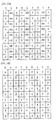
- FIG. 10A illustrates a light-induced deterioration predictive image signal of a 9 X 9 pixel area including pixels R, pixels G and pixels B in the area of the green box image in the experimental image of FIG. 3 .
- the pixel G displays a gray level of 255 (e.g. a substantially maximum luminance), and the pixel R and the pixel B do not emit light (e.g. a substantially minimum luminance).
- TFTs of the pixel R and the pixel B light-induced deterioration in which the voltage Vth of the pixel R and the pixel B is lowered due to a light output from the adjacent pixel G may occur.
- the light-induced deterioration analysis unit 51 detects the light-induced deterioration predictive image signal illustrated in FIG. 10A from an input image signal and transmits the light-induced deterioration predictive image signal to the gray level compensating value calculation unit 52.
- the light-induced deterioration predictive image signal is an image signal having display gray level values corresponding to pixels in a predetermined area. Although described herein with reference to a gray level table, the light-induced deterioration predictive image signal may be configured differently from the examples of the present invention described above.
- the gray level compensating value may be a gray level having a relatively low gray level value ranging from 2 to 8 that may turn on an adjacent pixel displaying an otherwise black gray level predicted to cause light-induced deterioration.
- an adjacent pixel of one pixel refers to a neighboring pixel sharing a boundary with the one pixel and a peripheral pixel of one pixel refers to a pixel in an area affected by a light output from said one pixel (e.g. a pixel that is close to but not necessarily adjacent to the one pixel).
- FIG. 10B is a light-induced deterioration gray level compensating value according to an embodiment of the present invention.
- a light-induced deterioration predictive image signal of FIG. 10A is displayed on the OLED display panel for a relatively long period of time, the voltage Vth of the driving TFTs of the pixel R and the pixel B may be lowered by the light-induced deterioration.
- the gray level compensating value calculation unit 52 assigns a gray level 0 to an image signal of the pixel G of which an input image gray level corresponds to a still image, and assigns a light-induced deterioration compensating value of a gray level 8 to image signals of the pixel R and the pixel B of which an input image gray level corresponds to a black image signal.
- a gray level 8 is selected as a light-induced deterioration compensating value by way of example, the light-induced deterioration gray level compensating value may have a different value that is determined according to a gray level value of a light emitting pixel and a distance with respect to the light emitting pixel.
- the light-induced deterioration gray level compensating value selected based on the gray level value of the light emitting pixel and the distance with respect to the light emitting pixel, as variables, may be separately stored in a gray level compensating value lookup table 53.
- the stored light-induced deterioration gray level compensating value may be referred to by the gray level compensating value calculation unit 52.
- the gray level compensating value calculation unit 52 transmits the selected light-induced deterioration gray level compensating value to the light-induced deterioration compensated image data generation unit 54.
- FIG. 10C illustrates a light-induced deterioration compensated image data compensated by the light-induced deterioration compensated image data generation unit 54.
- the light-induced deterioration compensated image data generation unit 54 compensates the input image signal R, G and B with the light-induced deterioration gray level compensating value transmitted from the gray level compensating value calculation unit 52 to generate the light-induced deterioration compensated image data R", G" and B". Referring to the light-induced deterioration compensated image data of FIG.
- the gray level of pixel R maintains a gray level value of 255 of the input signal
- the gray levels of the pixel G and the pixel B are set as a light-induced deterioration gray level compensating value of 8 generated by the gray level compensating value calculation unit 52.
- FIG. 11A is a light-induced deterioration predictive image signal according to an embodiment of the present invention
- FIG. 11B is a light-induced deterioration gray level compensating value according to an embodiment of the present invention
- FIG. 11C is a light-induced deterioration compensated image data according to an embodiment of the present invention.
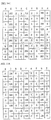
- the gray level of the pixel G is a gray level 128, and the gray levels of the pixel R and the pixel B adjacent to the pixel G has a gray level 0.
- the pixel G has a gray level 128, which is an intermediate value among a set of gray levels ranging from 0 to 255, and compared to the case of displaying a gray level 255, a maximum gray level, the pixel G displaying a gray level 128 may induce less light-induced deterioration in a non-light emitting pixel.
- the gray level compensating value calculation unit 52 assigns a gray level 0 to the gray level of the pixel G which is a light emitting pixel, and assigns a gray level 4 as the light-induced deterioration gray level compensating value to the gray levels of the pixel R and the pixel B which are non-light emitting pixels.
- the gray level compensating value calculation unit 52 may select a gray level 4, lower than a gray level 8, as the light-induced deterioration gray level compensating value, considering that the gray level value of the adjacent pixel G is a gray level 128.
- FIG. 11C is a light-induced deterioration compensated image data generated by the light-induced deterioration compensated image data generation unit 54.
- the light-induced deterioration compensated image data generation unit 54 compensates the light-induced deterioration predictive image signal illustrated in FIG. 11A with the light-induced deterioration gray level compensating value applied from the gray level compensating value calculation unit 52 illustrated in FIG. 11B to generate the light-induced deterioration compensated image data.
- the gray level of the pixel G maintains an input gray level value and the pixel R and the pixel B, which are vulnerable to light-induced deterioration, with the light-induced deterioration gray level compensating value of a gray level 4 generated from the gray level compensating value calculation unit 52.
- the pixel R and the pixel B applied with the light-induced deterioration compensated image data may emit light in a gray level 4, thereby rendering those pixels less influenced by the light-induced deterioration that may occur by the light output from the pixel G.
- FIG. 12 is a flowchart illustrating a method of compensating for light-induced deterioration according to an embodiment of the present invention.
- a light-induced deterioration compensated image data generation unit 54 may selectively output a light-induced deterioration compensated image data and a light-induced deterioration uncompensated image data so that a contrast of the OLED display device is not degraded by the light-induced deterioration compensation.
- the light-induced deterioration compensated image data generation unit 54 may alternately output the light-induced deterioration compensated image data and the light-induced deterioration uncompensated image data at periodic intervals.
- the light-induced deterioration analysis unit 51 receives an image signal to be displayed on the OLED display panel (S210).
- the input image signal is analyzed such that a light-induced deterioration predictive image signal is set (S220).
- the set light-induced deterioration predictive image signal is transmitted to the gray level compensating value calculation unit 52.
- the gray level compensating value calculation unit 52 sets a light-induced deterioration gray level compensating value of the image signal so that non-light emitting pixels that would otherwise be susceptible to light-induced deterioration may be compensated for and may thereby emit light (S230).
- the light-induced deterioration compensated image data generation unit 54 compensates the input light-induced deterioration predictive image signal with the light-induced deterioration gray level compensating value and outputs the light-induced deterioration compensated image data (S240).
- the light-induced deterioration compensated image data generation unit 54 counts light-induced deterioration compensating time during which the light-induced deterioration compensated image data is output (S250).
- the light-induced deterioration compensated image data generation unit 54 compares the light-induced deterioration compensating time with a preset reference time (S260). The light-induced deterioration compensated image data generation unit 54 outputs the light-induced deterioration compensated image data until the light-induced deterioration compensating time exceeds the preset reference time.
- the light-induced deterioration compensated image data generation unit 54 stops outputting the light-induced deterioration compensated image data, and outputs the light-induced deterioration uncompensated image data, generated from the input image signal, of which light-induced deterioration is not compensated (S270).
- the light-induced deterioration compensated image data generation unit 54 counts light-induced deterioration time while outputting the light-induced deterioration uncompensated image data (S280).
- the light-induced deterioration compensated image data generation unit 54 compares the light-induced deterioration time with a preset reference deterioration time (S290). When the light-induced deterioration time does not exceed the preset reference deterioration time, the light-induced deterioration compensated image data generation unit 54 outputs the light-induced deterioration uncompensated image data.
- the light-induced deterioration compensated image data generation unit 54 moves to a step of outputting a light-induced deterioration compensated image data reflecting the light-induced deterioration gray level compensating value.
- the light-induced deterioration compensated image data generation unit 54 alternately displays the light-induced deterioration compensated image data and the light-induced deterioration uncompensated image data periodically, the light-induced deterioration may be substantially prevented while maintaining a desired level of contrast within the screen in an OLED display device according to an embodiment of the present invention.
- FIG. 13A illustrates a first light-induced deterioration gray level compensating value according to an embodiment of the present invention
- FIG. 13B illustrates a second light-induced deterioration gray level compensating value according to an embodiment of the present invention.
- FIGS. 13A and 13B respectively illustrate first and second light-induced deterioration gray level compensating values each configured so that light-induced deterioration gray level compensating values alternate on the basis of horizontal line.
- the first light-induced deterioration gray level compensating value illustrated in FIG. 13A is configured so that the pixels R and the pixels B in odd-numbered horizontal lines are represented with a gray level 0, and the pixels R and the pixels B in even-numbered horizontal lines are represented with a gray level 8.
- the second light-induced deterioration gray level compensating value illustrated in FIG. 13B is configured so that the pixels R and the pixels B in odd-numbered horizontal lines are represented with a gray level 8, and the pixels R and the pixels B in even-numbered horizontal lines are represented with a gray level 0.
- the gray level compensating value calculation unit 52 alternately outputs the first light-induced deterioration gray level compensating value and the second light-induced deterioration gray level compensating value to be used for deterioration compensation in the light-induced deterioration compensated image data generation unit 54.
- the gray level compensating value calculation unit 52 alternately outputs the first light-induced deterioration gray level compensating value and the second light-induced deterioration gray level compensating value to be used for deterioration compensation in the light-induced deterioration compensated image data generation unit 54.
- pixels in upper and lower portions on the display screen alternately emit light with the light-induced deterioration gray level compensating value, light-induced deterioration may be compensated without causing contrast degradation.
- the first and second light-induced deterioration gray level compensating values in FIGS. 13A and 13B may be alternately output on the basis of an image frame.
- the light-induced deterioration gray level compensating value may be converted in synchronization with a time point at which an image configuration displayed on the screen changes through the image signal analysis.
- the image signal analysis may be determined by, for example, analyzing a histogram of an image information. When an amount of change of the histogram information for each color is at or above a predetermined level, it may be determined that conversion of a channel or an image cut occurs.
- a screen of the light-induced deterioration gray level compensating value being changed might not be easily recognized by a user.
- a method of converting the light-induced deterioration image pattern and the light-induced deterioration gray level compensation pattern may vary based on the degree of light-induced deterioration of the particular OLED display device and various other considerations.
- FIG. 14 is an explanatory view illustrating a light-induced deterioration compensation area of an OLED display panel 10 according to an embodiment of the present invention.
- the OLED display panel 10 displays a moving image of a car, and displays a logo of a broadcasting company at a fixed position on an upper right side. Since an image having a motion, like a car, has a mix of a light emitting state and a non-light emitting state of the pixel, a voltage Vth of a certain pixel may be rarely changed due to light-induced deterioration. However, a still image, such as a logo of a broadcasting company, which emits light with a high luminance at a substantially same position may cause light-induced deterioration in a non-emitting pixel in an area adjacent to a light emitting pixel area, such that luminance unevenness may occur in the OLED display panel 10.
- FIG. 15 illustrates an example of a light-induced deterioration predictive image signal of a display screen of FIG. 14 .
- a logo LOGO is displayed as a white character with a relatively high luminance whereby each of a pixel R, a pixel G, and a pixel B has a gray level of 255.
- An image signal of each of a pixel R, a pixel G, and a pixel B in the periphery of a light emitting pixel area in which the logo LOGO is displayed has a black gray level (e.g. a gray level 0).
- the logo LOGO is displayed on the OLED display panel 10 for a relatively long period of time and may be set as a light-induced deterioration predictive image signal.
- FIG. 16 is a light-induced deterioration compensated image data according to an embodiment of the present invention.
- the light-induced deterioration compensation unit 50 assigns a light-induced deterioration gray level compensating value of 8 to a non-light emitting pixel in the periphery of a light emitting pixel in which light-induced deterioration may occur according to the light-induced deterioration predictive image signal to generate a light-induced deterioration compensated image data.
- a light-induced gray level compensating value of 8 may be assigned to a non-light emitting pixel spaced apart from a light emitting pixel by 6 pixels.
- a range of the non-light emitting pixels in the peripheral area corresponds to a distance affected by a light output from the light emitting pixel, and may be experimentally determined based on light emission of the light emitting pixel, the size of the pixel, the distance between pixels, and characteristics of the pixel TFT.
- FIG. 17 illustrates a light-induced deterioration compensated image data according to an embodiment of the present invention.
- the light-induced deterioration compensation unit 50 assigns a light-induced gray level compensating value of 8 or 4 to a black image signal applied to a pixel spaced apart from a light emitting pixel according to the light-induced deterioration predictive image signal to generate a light-induced deterioration compensated image data.
- a degree of light-induced deterioration is proportional to an output light incident to pixels in the peripheral area, as a distance from the light emitting pixel increases, a lower light-induced deterioration gray level compensating value may be applied.
- the display screen of the light-induced deterioration compensated image data might not become rough.
- the light-induced deterioration gray level compensating value of two stages is taken as an example, but more steps may be set.
- a substantially same light-induced deterioration gray level compensating value may be assigned to a pixel R, a pixel G, and a pixel B so that color artifacts might not be visually recognized in a low gray level environment.
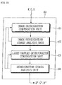
- FIG. 18 is a configuration view illustrating a deterioration compensation unit 60 according to an embodiment of the present invention.
- the deterioration compensation unit 60 may include an image deterioration compensation unit 61, an image deterioration stress analysis unit 62, a light-induced deterioration compensation unit 63, and a deterioration stress analysis unit 64.
- the image deterioration compensation unit 61 may substantially prevent deterioration of an organic light emitting layer of a pixel caused by a same pixel emitting light for a relatively long period of time.
- the image deterioration compensation unit 61 detects a still image and moves the display screen including the still image to an upper or lower and/or left or right direction by one to two unit pixels on the OLED display panel.
- the image deterioration compensation unit 61 may move the entire screen on the pixel basis or may move only a part of the entire screen where image sticking occurs.
- the image deterioration stress analysis unit 62 may analyze image deterioration occurring in the image screen moved by the image deterioration compensation unit 61.
- the image deterioration corresponds to a deterioration occurring in a light emitting pixel, and image sticking that may occur afterwards may be predicted through the image deterioration stress analysis.
- the image deterioration stress analysis unit 62 is configured to separately measure the influence of the image deterioration.
- the light-induced deterioration compensation unit 63 compensates for the light-induced deterioration occurring in a non-light emitting pixel in the periphery of a pixel that emits light for a relatively long period of time.
- the light-induced deterioration compensation unit 63 detects a still image and, when the still image is detected, compensates for an image signal so that the non-light emitting pixel in the peripheral area may emit light with a relatively low gray level.
- the deterioration stress analysis unit 64 analyzes deterioration stress of the image signal compensated by the image deterioration compensation unit 61 and the light-induced deterioration compensation unit 63.
- the image signals compensated for deterioration are accumulated and the accumulated image signals are modeled.
- the image signal modeling may include accumulating output image signals and converting them to a maximum gray level for an accumulation time. With respect to the converted maximum gray level for the accumulation time, a deterioration stress may be analyzed for each panel based on the characteristics of the panel.
- the deterioration stress analysis unit 64 transmits the deterioration stress for each panel to the image deterioration compensation unit 61 and/or the light-induced deterioration compensation unit 63.
- the image deterioration compensation unit 61 and the light-induced deterioration compensation unit 63 may determine whether to compensate for the deterioration and adjust the deterioration compensating value based on the deterioration stress applied thereto.
- FIG. 19 is a display image of an OLED display device according to an embodiment of the present invention.
- a data signal voltage of a gray level 31 31G
- the display image includes two red box images in the upper portion of the screen and two green box images below the two red box images, respectively.
- a pixel R represents a gray level 255 (e.g. a maximum brightness)
- a pixel G and a pixel B represent a gray level 8 (which is a relatively low gray level within the scale of 0 to 255).
- a pixel G represents 255 gray level
- a pixel R and a pixel B represent a gray level 8.
- a change in the voltage Vth due to light-induced deterioration may be suppressed and the luminance unevenness in the panel may be avoided by compensating for an image signal applied to a non-light emitting pixel in the periphery of a light emitting pixel area with the light-induced deterioration gray level compensating value of a relatively low gray level.
- an OLED display may analyze an image signal input to the OLED display device, detect a light-induced deterioration predictive image signal predicting possible light-induced deterioration, and compensate for a black image signal of the light-induced deterioration predictive image signal with a relatively low gray level, such that light-induced deterioration may be avoided.
Landscapes
- Engineering & Computer Science (AREA)
- Physics & Mathematics (AREA)
- Computer Hardware Design (AREA)
- General Physics & Mathematics (AREA)
- Theoretical Computer Science (AREA)
- Control Of El Displays (AREA)
- Electroluminescent Light Sources (AREA)
- Control Of Indicators Other Than Cathode Ray Tubes (AREA)
Claims (10)
- Anzeigevorrichtung vom Aktivmatrixtyp mit organischen Leuchtdioden (OLED), umfassend:eine Anzeigetafel mit organischen Leuchtdioden, die eine Vielzahl von Gate-Leitungen, eine Vielzahl von Datenleitungen, welche die Vielzahl von Gate-Leitungen kreuzen, und eine Vielzahl von Pixeln, die mit der Vielzahl von Gate-Leitungen und der Vielzahl von Datenleitungen verbunden sind, umfasst;eine Zeitsteuerungseinrichtung, die dafür konfiguriert ist, ein Bildsignal aus einer Vielzahl von Einzelbildern zu empfangen und Bilddaten auszugeben, die auf der Vielzahl von Einzelbildern beruhen; undeinen Datentreiber, der dafür konfiguriert ist, eine Datensignalspannung zu erzeugen, die den von der Zeitsteuerungseinrichtung ausgegebenen Bilddaten entspricht,worin eine Ausgleichseinheit für lichtinduzierte Verschlechterung in der Zeitsteuerungseinrichtung enthalten und dafür konfiguriert ist, zu ermitteln, ob das Bildsignal ein Schwarzbildsignal für ein Pixel aus der Vielzahl von Pixeln einschließt, das einen minimalen Graustufenwert aufweist, der für mindestens eine vorbestimmte Vielzahl von Einzelbildern fortbesteht;wobei die Ausgleichseinheit für lichtinduzierte Verschlechterung ferner dafür konfiguriert ist, zu ermitteln, ob das Bildsignal für ein an das eine Pixel angrenzendes Pixel einen Graustufenwert oberhalb eines Referenzgraustufenwertes einschließt, der für die vorbestimmte Vielzahl von Einzelbildern fortbesteht; undwobei die Ausgleichseinheit für lichtinduzierte Verschlechterung ferner dafür konfiguriert ist, als Reaktion auf das Ermitteln, dass beide genannten Bedingungen erfüllt sind, das Schwarzbildsignal durch Ausgeben von ersten Bilddaten an das eine Pixel zu konvertieren, worin die ersten Bilddaten einen ersten Graustufenwert aufweisen, der größer als der minimale Graustufenwert des Schwarzbildsignals ist.
- Anzeigevorrichtung mit organischen Leuchtdioden nach Anspruch 1, worin die vorbestimmte Vielzahl von Einzelbildern mindestens zehn aufeinanderfolgende Einzelbilder umfasst.
- Anzeigevorrichtung mit organischen Leuchtdioden nach Anspruch 1 oder 2, worin, wenn der minimale Graustufenwert des Bildsignals als ein Graustufenwert 0 ist und der maximale Graustufenwert des Bildsignals als ein Graustufenwert 255 definiert ist, das Schwarzbildsignal den Graustufenwert 0 aufweist.
- Anzeigevorrichtung mit organischen Leuchtdioden nach Anspruch 3, worin die ersten Bilddaten einen Graustufenwert im Bereich von 2 bis 8 aufweisen.
- Anzeigevorrichtung mit organischen Leuchtdioden nach einem der vorhergehenden Ansprüche, worin die Zeitsteuerungseinrichtung dafür konfiguriert ist, während der Vielzahl von Einzelbildern abwechselnd die ersten Bilddaten und zweite Bilddaten mit einem zweiten Graustufenwert, der sich vom ersten Graustufenwert unterscheidet, auszugeben.
- Anzeigevorrichtung mit organischen Leuchtdioden nach Anspruch 5, worin der zweite Graustufenwert gleich dem minimalen Graustufenwert des Schwarzbildsignals ist.
- Anzeigevorrichtung mit organischen Leuchtdioden nach Anspruch 1, worin die Ausgleichseinheit für lichtinduzierte Verschlechterung der Zeitsteuerungseinrichtung umfasst:eine Einheit zur Analyse der lichtinduzierten Verschlechterung, die dafür konfiguriert ist, als Reaktion auf das Ermitteln, dass beide Bedingungen erfüllt sind, ein Bildsignal mit Vorhersage der lichtinduzierten Verschlechterung einzustellen;eine Graustufenausgleichswert-Berechnungseinheit, die dafür konfiguriert ist, von der Einheit zur Analyse der lichtinduzierten Verschlechterung das Bildsignal mit Vorhersage der lichtinduzierten Verschlechterung zu empfangen und daraus einen Graustufenwertausgleichswert für die lichtinduzierte Verschlechterung zu berechnen; undeine Erzeugungseinheit für Bilddaten mit Ausgleich der lichtinduzierten Verschlechterung, die dafür konfiguriert ist, das Bildsignal mit Vorhersage der lichtinduzierten Verschlechterung mit dem Graustufenwertausgleichswert für die lichtinduzierte Verschlechterung auszugleichen, um Bilddaten mit Ausgleich der lichtinduzierten Verschlechterung zu erzeugen und auszugeben, die mit den ersten Bilddaten zusammenfallen.
- Anzeigevorrichtung mit organischen Leuchtdioden nach einem der vorhergehenden Ansprüche, worin das Pixel einen Dünnschichttransistor umfasst, der eine Oxidhalbleiterschicht umfasst.
- Anzeigevorrichtung mit organischen Leuchtdioden nach Anspruch 8, worin die Oxidhalbleiterschicht mindestens ein Material umfasst, das aus der Gruppe ausgewählt wird, die aus Folgendem besteht:: Zinkoxid (ZnO), Zink-Zinn-Oxid (ZTO), Zink-IndiumOxid (ZIO), Indiumoxid (InO), Titanoxid (TiO), Indium-Gallium-Zink-Oxid (IGZO) und Indium-Zink-Zinn-Oxid (IZTO).
- Verfahren zum Ausgleichen der lichtinduzierten Verschlechterung der Anzeigevorrichtung mit organischen Leuchtdioden (OLED) nach Anspruch 1, wobei das Verfahren umfasst:Empfangen eines Bildsignals, das Bildinformation umfasst;Ermitteln, ob das Bildsignal ein Schwarzbildsignal für ein Pixel aus der Vielzahl von Pixeln einschließt, das einen minimalen Graustufenwert aufweist, der für mindestens eine vorbestimmte Vielzahl von Einzelbildern fortbesteht;Ermitteln, ob das Bildsignal für ein an das eine Pixel angrenzendes Pixel einen Graustufenwert oberhalb eines Referenzgraustufenwertes einschließt, der für die vorbestimmte Vielzahl von Einzelbildern fortbesteht; undals Reaktion auf das Ermitteln, dass beide Bedingungen erfüllt sind, erfolgendes Konvertieren des Schwarzbildsignals durch Ausgeben von ersten Bilddaten an das eine Pixel, worin die ersten Bilddaten einen ersten Graustufenwert aufweisen, der größer als der minimale Graustufenwert des Schwarzbildsignals ist.
Applications Claiming Priority (1)
| Application Number | Priority Date | Filing Date | Title |
|---|---|---|---|
| KR1020160121537A KR102561188B1 (ko) | 2016-09-22 | 2016-09-22 | 표시장치 |
Publications (2)
| Publication Number | Publication Date |
|---|---|
| EP3300068A1 EP3300068A1 (de) | 2018-03-28 |
| EP3300068B1 true EP3300068B1 (de) | 2019-09-18 |
Family
ID=59955500
Family Applications (1)
| Application Number | Title | Priority Date | Filing Date |
|---|---|---|---|
| EP17192771.8A Active EP3300068B1 (de) | 2016-09-22 | 2017-09-22 | Anzeigevorrichtung mit organischen leuchtdioden |
Country Status (4)
| Country | Link |
|---|---|
| US (1) | US10354575B2 (de) |
| EP (1) | EP3300068B1 (de) |
| KR (1) | KR102561188B1 (de) |
| CN (1) | CN107871475B (de) |
Families Citing this family (23)
| Publication number | Priority date | Publication date | Assignee | Title |
|---|---|---|---|---|
| KR102552299B1 (ko) | 2018-08-31 | 2023-07-10 | 삼성디스플레이 주식회사 | 잔상 보상부, 이를 포함하는 표시 장치, 및 표시 장치의 구동 방법 |
| FR3087582B1 (fr) | 2018-10-22 | 2021-09-03 | Microoled | Dispositif d'affichage jour et nuit |
| KR102582060B1 (ko) * | 2018-11-06 | 2023-09-25 | 삼성디스플레이 주식회사 | 표시 장치 및 이의 구동 방법 |
| KR102740894B1 (ko) * | 2019-06-03 | 2024-12-13 | 삼성디스플레이 주식회사 | 표시 장치 |
| WO2021029469A1 (ko) * | 2019-08-14 | 2021-02-18 | 엘지전자 주식회사 | 디스플레이 장치 및 그의 동작 방법 |
| USD918860S1 (en) * | 2019-10-11 | 2021-05-11 | Vizio, Inc. | Low profile speaker |
| KR102741049B1 (ko) * | 2019-12-27 | 2024-12-09 | 엘지디스플레이 주식회사 | 표시 장치 |
| KR102747304B1 (ko) * | 2020-02-12 | 2025-01-02 | 삼성디스플레이 주식회사 | 표시 장치 및 이의 구동 방법 |
| KR102743326B1 (ko) * | 2020-04-29 | 2024-12-18 | 삼성디스플레이 주식회사 | 표시 장치 및 이의 구동 방법 |
| JP2021196448A (ja) * | 2020-06-11 | 2021-12-27 | レノボ・シンガポール・プライベート・リミテッド | 電子機器及び画面焼き付き補正制御方法 |
| US11250770B1 (en) * | 2020-09-18 | 2022-02-15 | Himax Technologies Limited | De-jaggy processing system and method for OLED display with curved space |
| KR102852267B1 (ko) * | 2020-10-06 | 2025-09-01 | 삼성디스플레이 주식회사 | 데이터 보상 회로, 이를 포함하는 표시 장치 및 이를 이용한 데이터 보상 방법 |
| US12277916B2 (en) * | 2020-10-06 | 2025-04-15 | Samsung Display Co., Ltd. | Data compensating circuit, display device including the same, and method of compensating data using the same |
| US12211434B2 (en) | 2021-08-13 | 2025-01-28 | Samsung Electronics Co., Ltd. | Detecting stationary regions for organic light emitting diode (OLED) television (TV) luminance reduction |
| US12260526B2 (en) | 2021-08-13 | 2025-03-25 | Samsung Electronics Co., Ltd. | Self-emitting display (SED) burn-in prevention based on stationary luminance reduction |
| US12367565B2 (en) | 2021-08-18 | 2025-07-22 | Samsung Electronics Co., Ltd. | Efficient inverse tone mapping network for standard dynamic range (SDR) to high dynamic range (HDR) conversion on HDR display |
| CN116469344B (zh) * | 2022-01-12 | 2026-01-06 | 联咏科技股份有限公司 | 显示设备、面板驱动电路及显示驱动方法 |
| KR20230146160A (ko) * | 2022-04-11 | 2023-10-19 | 삼성디스플레이 주식회사 | 표시 장치 및 그 구동 방법 |
| US12051364B2 (en) * | 2022-05-06 | 2024-07-30 | Samsung Electronics Co., Ltd. | Organic light emitting diode (OLED) burn-in prevention based on stationary pixel and luminance reduction |
| KR20250060677A (ko) * | 2023-10-26 | 2025-05-07 | 엘지디스플레이 주식회사 | 발광표시패널 및 이를 이용한 발광표시장치 |
| KR20250096149A (ko) * | 2023-12-20 | 2025-06-27 | 엘지디스플레이 주식회사 | 디스플레이 장치 |
| CN118401053B (zh) * | 2024-04-19 | 2025-05-02 | 惠科股份有限公司 | 有机发光显示面板、显示装置及其驱动方法 |
| US20260120623A1 (en) * | 2024-10-24 | 2026-04-30 | Samsung Display Co., Ltd. | Display device and electronic device including the same |
Family Cites Families (20)
| Publication number | Priority date | Publication date | Assignee | Title |
|---|---|---|---|---|
| JPS532915A (en) | 1976-06-29 | 1978-01-12 | Asahi Boodo Kougiyou Kk | Tile panel |
| JP2000209506A (ja) * | 1999-01-14 | 2000-07-28 | Toshiba Corp | 撮像装置および撮像方法 |
| CN100386792C (zh) | 2002-03-04 | 2008-05-07 | 三洋电机株式会社 | 有机电致发光显示装置及其应用 |
| US20070109284A1 (en) * | 2005-08-12 | 2007-05-17 | Semiconductor Energy Laboratory Co., Ltd. | Display device |
| JP2008256954A (ja) * | 2007-04-05 | 2008-10-23 | Hitachi Displays Ltd | 表示装置 |
| KR101487548B1 (ko) * | 2007-05-18 | 2015-01-29 | 소니 주식회사 | 표시 장치, 표시 장치의 제어 방법 및 컴퓨터 프로그램이 기록된 기록 매체 |
| JP5213554B2 (ja) * | 2008-07-10 | 2013-06-19 | キヤノン株式会社 | 表示装置及びその駆動方法 |
| JP5484853B2 (ja) * | 2008-10-10 | 2014-05-07 | 株式会社半導体エネルギー研究所 | 半導体装置の作製方法 |
| JP5302915B2 (ja) | 2009-03-18 | 2013-10-02 | パナソニック株式会社 | 有機el表示装置及び制御方法 |
| JP5313066B2 (ja) * | 2009-07-07 | 2013-10-09 | レノボ・シンガポール・プライベート・リミテッド | 画素の焼き付きを防ぐ電子機器 |
| JP5531496B2 (ja) * | 2009-08-18 | 2014-06-25 | セイコーエプソン株式会社 | 画像処理装置、表示システム、電子機器及び画像処理方法 |
| JP2011107410A (ja) * | 2009-11-17 | 2011-06-02 | Sony Corp | 画像表示装置および画像表示方法 |
| US9466240B2 (en) * | 2011-05-26 | 2016-10-11 | Ignis Innovation Inc. | Adaptive feedback system for compensating for aging pixel areas with enhanced estimation speed |
| US8937632B2 (en) * | 2012-02-03 | 2015-01-20 | Ignis Innovation Inc. | Driving system for active-matrix displays |
| KR102122534B1 (ko) | 2013-12-24 | 2020-06-12 | 엘지디스플레이 주식회사 | 유기발광표시장치 및 이의 동작방법 |
| KR102172392B1 (ko) | 2014-06-27 | 2020-11-02 | 엘지디스플레이 주식회사 | 구동 소자의 열화를 보상할 수 있는 유기발광 표시장치 |
| KR102270460B1 (ko) * | 2014-09-19 | 2021-06-29 | 삼성디스플레이 주식회사 | 유기 발광 표시 장치 및 이의 열화 보상 방법 |
| KR102288794B1 (ko) * | 2015-01-27 | 2021-08-12 | 삼성디스플레이 주식회사 | 평균 전류 추출 방법 및 이를 포함하는 영상 정보 보상 방법 |
| CN104795015B (zh) * | 2015-04-21 | 2018-10-02 | 青岛海信电器股份有限公司 | 一种图像显示驱动方法、装置及设备 |
| KR102339647B1 (ko) | 2015-08-18 | 2021-12-15 | 엘지디스플레이 주식회사 | 표시장치 및 그의 데이터 보상방법 |
-
2016
- 2016-09-22 KR KR1020160121537A patent/KR102561188B1/ko active Active
-
2017
- 2017-09-19 US US15/708,976 patent/US10354575B2/en active Active
- 2017-09-22 CN CN201710864556.9A patent/CN107871475B/zh active Active
- 2017-09-22 EP EP17192771.8A patent/EP3300068B1/de active Active
Non-Patent Citations (1)
| Title |
|---|
| None * |
Also Published As
| Publication number | Publication date |
|---|---|
| KR102561188B1 (ko) | 2023-07-28 |
| KR20180032720A (ko) | 2018-04-02 |
| CN107871475A (zh) | 2018-04-03 |
| US10354575B2 (en) | 2019-07-16 |
| EP3300068A1 (de) | 2018-03-28 |
| US20180082625A1 (en) | 2018-03-22 |
| CN107871475B (zh) | 2022-05-13 |
Similar Documents
| Publication | Publication Date | Title |
|---|---|---|
| US10354575B2 (en) | Organic light emitting diode display device | |
| US10643537B2 (en) | Organic light-emitting display device | |
| US9412304B2 (en) | Display device and method for driving the same | |
| US11562692B2 (en) | Display device and a driving method thereof | |
| US8427513B2 (en) | Display device, display device drive method, and computer program | |
| EP1994522B1 (de) | Antriebsvorrichtung und antriebsverfahren für eine anzeigevorrichtung | |
| US8941695B2 (en) | Display device, driving method of display device, and electronic apparatus | |
| KR20160007786A (ko) | 표시장치 | |
| US11170712B2 (en) | Display device for adjusting black insertion for reducing power consumption | |
| US11295675B2 (en) | Display device and method of compensating pixel deterioration thereof | |
| KR20180003790A (ko) | Oled 표시 장치의 화질 보상 장치 및 보상 방법 | |
| KR20160007883A (ko) | 표시장치 | |
| KR20160056234A (ko) | 유기전계 발광표시장치 및 이의 구동방법 | |
| KR102470373B1 (ko) | 유기발광표시장치 | |
| US20170301294A1 (en) | Display device | |
| WO2015029337A1 (ja) | 表示制御装置 | |
| KR102717812B1 (ko) | 발광 표시 장치 및 그 구동 방법 | |
| KR102581863B1 (ko) | 표시장치 및 그의 구동방법 | |
| US12361882B2 (en) | Electroluminescent display apparatus and method of driving the same | |
| US20250329297A1 (en) | Control device, display device, and control method | |
| KR102212458B1 (ko) | 유기 발광 표시 장치 및 그 구동 방법 | |
| KR20110061775A (ko) | 액정표시장치 및 그 구동방법 |
Legal Events
| Date | Code | Title | Description |
|---|---|---|---|
| PUAI | Public reference made under article 153(3) epc to a published international application that has entered the european phase |
Free format text: ORIGINAL CODE: 0009012 |
|
| STAA | Information on the status of an ep patent application or granted ep patent |
Free format text: STATUS: THE APPLICATION HAS BEEN PUBLISHED |
|
| AK | Designated contracting states |
Kind code of ref document: A1 Designated state(s): AL AT BE BG CH CY CZ DE DK EE ES FI FR GB GR HR HU IE IS IT LI LT LU LV MC MK MT NL NO PL PT RO RS SE SI SK SM TR |
|
| AX | Request for extension of the european patent |
Extension state: BA ME |
|
| STAA | Information on the status of an ep patent application or granted ep patent |
Free format text: STATUS: REQUEST FOR EXAMINATION WAS MADE |
|
| 17P | Request for examination filed |
Effective date: 20180927 |
|
| RBV | Designated contracting states (corrected) |
Designated state(s): AL AT BE BG CH CY CZ DE DK EE ES FI FR GB GR HR HU IE IS IT LI LT LU LV MC MK MT NL NO PL PT RO RS SE SI SK SM TR |
|
| GRAP | Despatch of communication of intention to grant a patent |
Free format text: ORIGINAL CODE: EPIDOSNIGR1 |
|
| STAA | Information on the status of an ep patent application or granted ep patent |
Free format text: STATUS: GRANT OF PATENT IS INTENDED |
|
| INTG | Intention to grant announced |
Effective date: 20190328 |
|
| RIN1 | Information on inventor provided before grant (corrected) |
Inventor name: PARK, JINWOO Inventor name: YANG, SUMIN Inventor name: BAE, MINSEOK |
|
| GRAS | Grant fee paid |
Free format text: ORIGINAL CODE: EPIDOSNIGR3 |
|
| GRAA | (expected) grant |
Free format text: ORIGINAL CODE: 0009210 |
|
| STAA | Information on the status of an ep patent application or granted ep patent |
Free format text: STATUS: THE PATENT HAS BEEN GRANTED |
|
| AK | Designated contracting states |
Kind code of ref document: B1 Designated state(s): AL AT BE BG CH CY CZ DE DK EE ES FI FR GB GR HR HU IE IS IT LI LT LU LV MC MK MT NL NO PL PT RO RS SE SI SK SM TR |
|
| REG | Reference to a national code |
Ref country code: GB Ref legal event code: FG4D |
|
| REG | Reference to a national code |
Ref country code: CH Ref legal event code: EP |
|
| REG | Reference to a national code |
Ref country code: DE Ref legal event code: R096 Ref document number: 602017007130 Country of ref document: DE |
|
| REG | Reference to a national code |
Ref country code: AT Ref legal event code: REF Ref document number: 1182236 Country of ref document: AT Kind code of ref document: T Effective date: 20191015 |
|
| REG | Reference to a national code |
Ref country code: IE Ref legal event code: FG4D |
|
| REG | Reference to a national code |
Ref country code: NL Ref legal event code: FP |
|
| PG25 | Lapsed in a contracting state [announced via postgrant information from national office to epo] |
Ref country code: SE Free format text: LAPSE BECAUSE OF FAILURE TO SUBMIT A TRANSLATION OF THE DESCRIPTION OR TO PAY THE FEE WITHIN THE PRESCRIBED TIME-LIMIT Effective date: 20190918 Ref country code: HR Free format text: LAPSE BECAUSE OF FAILURE TO SUBMIT A TRANSLATION OF THE DESCRIPTION OR TO PAY THE FEE WITHIN THE PRESCRIBED TIME-LIMIT Effective date: 20190918 Ref country code: LT Free format text: LAPSE BECAUSE OF FAILURE TO SUBMIT A TRANSLATION OF THE DESCRIPTION OR TO PAY THE FEE WITHIN THE PRESCRIBED TIME-LIMIT Effective date: 20190918 Ref country code: FI Free format text: LAPSE BECAUSE OF FAILURE TO SUBMIT A TRANSLATION OF THE DESCRIPTION OR TO PAY THE FEE WITHIN THE PRESCRIBED TIME-LIMIT Effective date: 20190918 Ref country code: BG Free format text: LAPSE BECAUSE OF FAILURE TO SUBMIT A TRANSLATION OF THE DESCRIPTION OR TO PAY THE FEE WITHIN THE PRESCRIBED TIME-LIMIT Effective date: 20191218 Ref country code: NO Free format text: LAPSE BECAUSE OF FAILURE TO SUBMIT A TRANSLATION OF THE DESCRIPTION OR TO PAY THE FEE WITHIN THE PRESCRIBED TIME-LIMIT Effective date: 20191218 |
|
| REG | Reference to a national code |
Ref country code: LT Ref legal event code: MG4D |
|
| PG25 | Lapsed in a contracting state [announced via postgrant information from national office to epo] |
Ref country code: GR Free format text: LAPSE BECAUSE OF FAILURE TO SUBMIT A TRANSLATION OF THE DESCRIPTION OR TO PAY THE FEE WITHIN THE PRESCRIBED TIME-LIMIT Effective date: 20191219 Ref country code: RS Free format text: LAPSE BECAUSE OF FAILURE TO SUBMIT A TRANSLATION OF THE DESCRIPTION OR TO PAY THE FEE WITHIN THE PRESCRIBED TIME-LIMIT Effective date: 20190918 Ref country code: LV Free format text: LAPSE BECAUSE OF FAILURE TO SUBMIT A TRANSLATION OF THE DESCRIPTION OR TO PAY THE FEE WITHIN THE PRESCRIBED TIME-LIMIT Effective date: 20190918 Ref country code: AL Free format text: LAPSE BECAUSE OF FAILURE TO SUBMIT A TRANSLATION OF THE DESCRIPTION OR TO PAY THE FEE WITHIN THE PRESCRIBED TIME-LIMIT Effective date: 20190918 |
|
| REG | Reference to a national code |
Ref country code: AT Ref legal event code: MK05 Ref document number: 1182236 Country of ref document: AT Kind code of ref document: T Effective date: 20190918 |
|
| PG25 | Lapsed in a contracting state [announced via postgrant information from national office to epo] |
Ref country code: ES Free format text: LAPSE BECAUSE OF FAILURE TO SUBMIT A TRANSLATION OF THE DESCRIPTION OR TO PAY THE FEE WITHIN THE PRESCRIBED TIME-LIMIT Effective date: 20190918 Ref country code: RO Free format text: LAPSE BECAUSE OF FAILURE TO SUBMIT A TRANSLATION OF THE DESCRIPTION OR TO PAY THE FEE WITHIN THE PRESCRIBED TIME-LIMIT Effective date: 20190918 Ref country code: AT Free format text: LAPSE BECAUSE OF FAILURE TO SUBMIT A TRANSLATION OF THE DESCRIPTION OR TO PAY THE FEE WITHIN THE PRESCRIBED TIME-LIMIT Effective date: 20190918 Ref country code: PL Free format text: LAPSE BECAUSE OF FAILURE TO SUBMIT A TRANSLATION OF THE DESCRIPTION OR TO PAY THE FEE WITHIN THE PRESCRIBED TIME-LIMIT Effective date: 20190918 Ref country code: EE Free format text: LAPSE BECAUSE OF FAILURE TO SUBMIT A TRANSLATION OF THE DESCRIPTION OR TO PAY THE FEE WITHIN THE PRESCRIBED TIME-LIMIT Effective date: 20190918 Ref country code: PT Free format text: LAPSE BECAUSE OF FAILURE TO SUBMIT A TRANSLATION OF THE DESCRIPTION OR TO PAY THE FEE WITHIN THE PRESCRIBED TIME-LIMIT Effective date: 20200120 Ref country code: IT Free format text: LAPSE BECAUSE OF FAILURE TO SUBMIT A TRANSLATION OF THE DESCRIPTION OR TO PAY THE FEE WITHIN THE PRESCRIBED TIME-LIMIT Effective date: 20190918 |
|
| PG25 | Lapsed in a contracting state [announced via postgrant information from national office to epo] |
Ref country code: IS Free format text: LAPSE BECAUSE OF FAILURE TO SUBMIT A TRANSLATION OF THE DESCRIPTION OR TO PAY THE FEE WITHIN THE PRESCRIBED TIME-LIMIT Effective date: 20200224 Ref country code: SM Free format text: LAPSE BECAUSE OF FAILURE TO SUBMIT A TRANSLATION OF THE DESCRIPTION OR TO PAY THE FEE WITHIN THE PRESCRIBED TIME-LIMIT Effective date: 20190918 Ref country code: SK Free format text: LAPSE BECAUSE OF FAILURE TO SUBMIT A TRANSLATION OF THE DESCRIPTION OR TO PAY THE FEE WITHIN THE PRESCRIBED TIME-LIMIT Effective date: 20190918 Ref country code: CZ Free format text: LAPSE BECAUSE OF FAILURE TO SUBMIT A TRANSLATION OF THE DESCRIPTION OR TO PAY THE FEE WITHIN THE PRESCRIBED TIME-LIMIT Effective date: 20190918 |
|
| REG | Reference to a national code |
Ref country code: DE Ref legal event code: R097 Ref document number: 602017007130 Country of ref document: DE |
|
| PLBE | No opposition filed within time limit |
Free format text: ORIGINAL CODE: 0009261 |
|
| STAA | Information on the status of an ep patent application or granted ep patent |
Free format text: STATUS: NO OPPOSITION FILED WITHIN TIME LIMIT |
|
| PG2D | Information on lapse in contracting state deleted |
Ref country code: IS |
|
| PG25 | Lapsed in a contracting state [announced via postgrant information from national office to epo] |
Ref country code: IS Free format text: LAPSE BECAUSE OF FAILURE TO SUBMIT A TRANSLATION OF THE DESCRIPTION OR TO PAY THE FEE WITHIN THE PRESCRIBED TIME-LIMIT Effective date: 20200119 Ref country code: LU Free format text: LAPSE BECAUSE OF NON-PAYMENT OF DUE FEES Effective date: 20190922 Ref country code: DK Free format text: LAPSE BECAUSE OF FAILURE TO SUBMIT A TRANSLATION OF THE DESCRIPTION OR TO PAY THE FEE WITHIN THE PRESCRIBED TIME-LIMIT Effective date: 20190918 Ref country code: IE Free format text: LAPSE BECAUSE OF NON-PAYMENT OF DUE FEES Effective date: 20190922 |
|
| REG | Reference to a national code |
Ref country code: BE Ref legal event code: MM Effective date: 20190930 |
|
| 26N | No opposition filed |
Effective date: 20200619 |
|
| PG25 | Lapsed in a contracting state [announced via postgrant information from national office to epo] |
Ref country code: MC Free format text: LAPSE BECAUSE OF FAILURE TO SUBMIT A TRANSLATION OF THE DESCRIPTION OR TO PAY THE FEE WITHIN THE PRESCRIBED TIME-LIMIT Effective date: 20190918 Ref country code: BE Free format text: LAPSE BECAUSE OF NON-PAYMENT OF DUE FEES Effective date: 20190930 Ref country code: SI Free format text: LAPSE BECAUSE OF FAILURE TO SUBMIT A TRANSLATION OF THE DESCRIPTION OR TO PAY THE FEE WITHIN THE PRESCRIBED TIME-LIMIT Effective date: 20190918 |
|
| REG | Reference to a national code |
Ref country code: CH Ref legal event code: PL |
|
| PG25 | Lapsed in a contracting state [announced via postgrant information from national office to epo] |
Ref country code: CY Free format text: LAPSE BECAUSE OF FAILURE TO SUBMIT A TRANSLATION OF THE DESCRIPTION OR TO PAY THE FEE WITHIN THE PRESCRIBED TIME-LIMIT Effective date: 20190918 |
|
| PG25 | Lapsed in a contracting state [announced via postgrant information from national office to epo] |
Ref country code: HU Free format text: LAPSE BECAUSE OF FAILURE TO SUBMIT A TRANSLATION OF THE DESCRIPTION OR TO PAY THE FEE WITHIN THE PRESCRIBED TIME-LIMIT; INVALID AB INITIO Effective date: 20170922 Ref country code: MT Free format text: LAPSE BECAUSE OF FAILURE TO SUBMIT A TRANSLATION OF THE DESCRIPTION OR TO PAY THE FEE WITHIN THE PRESCRIBED TIME-LIMIT Effective date: 20190918 |
|
| PG25 | Lapsed in a contracting state [announced via postgrant information from national office to epo] |
Ref country code: CH Free format text: LAPSE BECAUSE OF NON-PAYMENT OF DUE FEES Effective date: 20200930 Ref country code: LI Free format text: LAPSE BECAUSE OF NON-PAYMENT OF DUE FEES Effective date: 20200930 |
|
| PG25 | Lapsed in a contracting state [announced via postgrant information from national office to epo] |
Ref country code: TR Free format text: LAPSE BECAUSE OF FAILURE TO SUBMIT A TRANSLATION OF THE DESCRIPTION OR TO PAY THE FEE WITHIN THE PRESCRIBED TIME-LIMIT Effective date: 20190918 |
|
| PG25 | Lapsed in a contracting state [announced via postgrant information from national office to epo] |
Ref country code: MK Free format text: LAPSE BECAUSE OF FAILURE TO SUBMIT A TRANSLATION OF THE DESCRIPTION OR TO PAY THE FEE WITHIN THE PRESCRIBED TIME-LIMIT Effective date: 20190918 |
|
| P01 | Opt-out of the competence of the unified patent court (upc) registered |
Effective date: 20230516 |
|
| PGFP | Annual fee paid to national office [announced via postgrant information from national office to epo] |
Ref country code: NL Payment date: 20250821 Year of fee payment: 9 |
|
| PGFP | Annual fee paid to national office [announced via postgrant information from national office to epo] |
Ref country code: DE Payment date: 20250820 Year of fee payment: 9 |
|
| PGFP | Annual fee paid to national office [announced via postgrant information from national office to epo] |
Ref country code: GB Payment date: 20250820 Year of fee payment: 9 |
|
| PGFP | Annual fee paid to national office [announced via postgrant information from national office to epo] |
Ref country code: FR Payment date: 20250821 Year of fee payment: 9 |