EP3299943A1 - Conductor-layer-equipped structure, and touch panel - Google Patents
Conductor-layer-equipped structure, and touch panel Download PDFInfo
- Publication number
- EP3299943A1 EP3299943A1 EP16796510.2A EP16796510A EP3299943A1 EP 3299943 A1 EP3299943 A1 EP 3299943A1 EP 16796510 A EP16796510 A EP 16796510A EP 3299943 A1 EP3299943 A1 EP 3299943A1
- Authority
- EP
- European Patent Office
- Prior art keywords
- layer
- resin layer
- conductor
- resin
- wiring body
- Prior art date
- Legal status (The legal status is an assumption and is not a legal conclusion. Google has not performed a legal analysis and makes no representation as to the accuracy of the status listed.)
- Withdrawn
Links
Images





Classifications
-
- G—PHYSICS
- G06—COMPUTING OR CALCULATING; COUNTING
- G06F—ELECTRIC DIGITAL DATA PROCESSING
- G06F3/00—Input arrangements for transferring data to be processed into a form capable of being handled by the computer; Output arrangements for transferring data from processing unit to output unit, e.g. interface arrangements
- G06F3/01—Input arrangements or combined input and output arrangements for interaction between user and computer
- G06F3/03—Arrangements for converting the position or the displacement of a member into a coded form
- G06F3/041—Digitisers, e.g. for touch screens or touch pads, characterised by the transducing means
- G06F3/044—Digitisers, e.g. for touch screens or touch pads, characterised by the transducing means by capacitive means
- G06F3/0445—Digitisers, e.g. for touch screens or touch pads, characterised by the transducing means by capacitive means using two or more layers of sensing electrodes, e.g. using two layers of electrodes separated by a dielectric layer
-
- B—PERFORMING OPERATIONS; TRANSPORTING
- B32—LAYERED PRODUCTS
- B32B—LAYERED PRODUCTS, i.e. PRODUCTS BUILT-UP OF STRATA OF FLAT OR NON-FLAT, e.g. CELLULAR OR HONEYCOMB, FORM
- B32B27/00—Layered products comprising a layer of synthetic resin
- B32B27/06—Layered products comprising a layer of synthetic resin as the main or only constituent of a layer, which is next to another layer of the same or of a different material
- B32B27/08—Layered products comprising a layer of synthetic resin as the main or only constituent of a layer, which is next to another layer of the same or of a different material of synthetic resin
-
- G—PHYSICS
- G06—COMPUTING OR CALCULATING; COUNTING
- G06F—ELECTRIC DIGITAL DATA PROCESSING
- G06F3/00—Input arrangements for transferring data to be processed into a form capable of being handled by the computer; Output arrangements for transferring data from processing unit to output unit, e.g. interface arrangements
- G06F3/01—Input arrangements or combined input and output arrangements for interaction between user and computer
- G06F3/03—Arrangements for converting the position or the displacement of a member into a coded form
- G06F3/041—Digitisers, e.g. for touch screens or touch pads, characterised by the transducing means
- G06F3/044—Digitisers, e.g. for touch screens or touch pads, characterised by the transducing means by capacitive means
- G06F3/0446—Digitisers, e.g. for touch screens or touch pads, characterised by the transducing means by capacitive means using a grid-like structure of electrodes in at least two directions, e.g. using row and column electrodes
-
- H—ELECTRICITY
- H01—ELECTRIC ELEMENTS
- H01B—CABLES; CONDUCTORS; INSULATORS; SELECTION OF MATERIALS FOR THEIR CONDUCTIVE, INSULATING OR DIELECTRIC PROPERTIES
- H01B13/00—Apparatus or processes specially adapted for manufacturing conductors or cables
-
- H—ELECTRICITY
- H01—ELECTRIC ELEMENTS
- H01B—CABLES; CONDUCTORS; INSULATORS; SELECTION OF MATERIALS FOR THEIR CONDUCTIVE, INSULATING OR DIELECTRIC PROPERTIES
- H01B5/00—Non-insulated conductors or conductive bodies characterised by their form
- H01B5/14—Non-insulated conductors or conductive bodies characterised by their form comprising conductive layers or films on insulating-supports
-
- H—ELECTRICITY
- H01—ELECTRIC ELEMENTS
- H01B—CABLES; CONDUCTORS; INSULATORS; SELECTION OF MATERIALS FOR THEIR CONDUCTIVE, INSULATING OR DIELECTRIC PROPERTIES
- H01B7/00—Insulated conductors or cables characterised by their form
- H01B7/02—Disposition of insulation
-
- H—ELECTRICITY
- H03—ELECTRONIC CIRCUITRY
- H03K—PULSE TECHNIQUE
- H03K17/00—Electronic switching or gating, i.e. not by contact-making and –breaking
- H03K17/94—Electronic switching or gating, i.e. not by contact-making and –breaking characterised by the way in which the control signals are generated
- H03K17/96—Touch switches
- H03K17/962—Capacitive touch switches
-
- B—PERFORMING OPERATIONS; TRANSPORTING
- B32—LAYERED PRODUCTS
- B32B—LAYERED PRODUCTS, i.e. PRODUCTS BUILT-UP OF STRATA OF FLAT OR NON-FLAT, e.g. CELLULAR OR HONEYCOMB, FORM
- B32B2307/00—Properties of the layers or laminate
- B32B2307/20—Properties of the layers or laminate having particular electrical or magnetic properties, e.g. piezoelectric
- B32B2307/202—Conductive
-
- B—PERFORMING OPERATIONS; TRANSPORTING
- B32—LAYERED PRODUCTS
- B32B—LAYERED PRODUCTS, i.e. PRODUCTS BUILT-UP OF STRATA OF FLAT OR NON-FLAT, e.g. CELLULAR OR HONEYCOMB, FORM
- B32B2457/00—Electrical equipment
- B32B2457/20—Displays, e.g. liquid crystal displays, plasma displays
- B32B2457/208—Touch screens
-
- G—PHYSICS
- G02—OPTICS
- G02F—OPTICAL DEVICES OR ARRANGEMENTS FOR THE CONTROL OF LIGHT BY MODIFICATION OF THE OPTICAL PROPERTIES OF THE MEDIA OF THE ELEMENTS INVOLVED THEREIN; NON-LINEAR OPTICS; FREQUENCY-CHANGING OF LIGHT; OPTICAL LOGIC ELEMENTS; OPTICAL ANALOGUE/DIGITAL CONVERTERS
- G02F1/00—Devices or arrangements for the control of the intensity, colour, phase, polarisation or direction of light arriving from an independent light source, e.g. switching, gating or modulating; Non-linear optics
- G02F1/01—Devices or arrangements for the control of the intensity, colour, phase, polarisation or direction of light arriving from an independent light source, e.g. switching, gating or modulating; Non-linear optics for the control of the intensity, phase, polarisation or colour
- G02F1/13—Devices or arrangements for the control of the intensity, colour, phase, polarisation or direction of light arriving from an independent light source, e.g. switching, gating or modulating; Non-linear optics for the control of the intensity, phase, polarisation or colour based on liquid crystals, e.g. single liquid crystal display cells
- G02F1/133—Constructional arrangements; Operation of liquid crystal cells; Circuit arrangements
- G02F1/1333—Constructional arrangements; Manufacturing methods
- G02F1/13338—Input devices, e.g. touch panels
-
- G—PHYSICS
- G06—COMPUTING OR CALCULATING; COUNTING
- G06F—ELECTRIC DIGITAL DATA PROCESSING
- G06F2203/00—Indexing scheme relating to G06F3/00 - G06F3/048
- G06F2203/041—Indexing scheme relating to G06F3/041 - G06F3/045
- G06F2203/04103—Manufacturing, i.e. details related to manufacturing processes specially suited for touch sensitive devices
-
- G—PHYSICS
- G06—COMPUTING OR CALCULATING; COUNTING
- G06F—ELECTRIC DIGITAL DATA PROCESSING
- G06F2203/00—Indexing scheme relating to G06F3/00 - G06F3/048
- G06F2203/041—Indexing scheme relating to G06F3/041 - G06F3/045
- G06F2203/04111—Cross over in capacitive digitiser, i.e. details of structures for connecting electrodes of the sensing pattern where the connections cross each other, e.g. bridge structures comprising an insulating layer, or vias through substrate
-
- G—PHYSICS
- G06—COMPUTING OR CALCULATING; COUNTING
- G06F—ELECTRIC DIGITAL DATA PROCESSING
- G06F2203/00—Indexing scheme relating to G06F3/00 - G06F3/048
- G06F2203/041—Indexing scheme relating to G06F3/041 - G06F3/045
- G06F2203/04112—Electrode mesh in capacitive digitiser: electrode for touch sensing is formed of a mesh of very fine, normally metallic, interconnected lines that are almost invisible to see. This provides a quite large but transparent electrode surface, without need for ITO or similar transparent conductive material
-
- H—ELECTRICITY
- H01—ELECTRIC ELEMENTS
- H01B—CABLES; CONDUCTORS; INSULATORS; SELECTION OF MATERIALS FOR THEIR CONDUCTIVE, INSULATING OR DIELECTRIC PROPERTIES
- H01B13/00—Apparatus or processes specially adapted for manufacturing conductors or cables
- H01B13/0036—Details
Definitions
- the present invention relates to a conductor-layer-equipped structure and a touch panel.
- Patent Application No. 2015-103090 filed with Japan Patent Office on May 20, 2015
- Patent Application No. 2016-18726 filed with Japan Patent Office on February 3, 2016, are incorporated herein by reference in the designated countries in which the incorporation by reference is accepted.
- a sensor film for touch panels which is configured such that a conductor pattern layer is laid on a transparent board having a retardation of 6,000 nm or more (see Patent Document 1, for example).
- the above sensor film uses a transparent board having a retardation value of 6,000 nm or more, that is, having optical anisotropy.
- a transparent board having a large retardation value is an expensive material, which may be problematic.
- Problems to be solved by the present invention include providing a conductor-layer-equipped structure and touch panel that are capable of suppressing the deterioration in visibility while reducing the cost.
- the first resin layer and the second resin layer are composed of materials having optical isotropy.
- the birefringence for light incident on the wiring body is therefore suppressed.
- the material constituting the first resin layer and the material constituting the second resin layer have the same composition.
- the occurrence of scattering or the like of the incident light is therefore suppressed at the interface between the first and second resin layers. This can suppress the deterioration in visibility of the conductor-layer-equipped structure.
- the cost can be reduced because it is not necessary to use an expensive material having optical anisotropy and thus having a high retardation value.
- the first conductor layer is supported by the first resin layer. It is therefore not necessary to use a base material or the like that is provided to directly adhere to the wiring body for supporting the first conductor layer. Thus, the deterioration in visibility of the conductor-layer-equipped structure can be suppressed and the conductor-layer-equipped structure can be made thin.
- FIG. 1 is a transparent perspective view illustrating an input device according to an embodiment of the present invention.
- the input device 1 has a function of detecting the operation position of an operator (position detection function) using a capacitance scheme and, as illustrated in FIG. 1 , includes a conductor-layer-equipped structure 2.
- An image display device (not illustrated) is disposed at one side of the conductor-layer-equipped structure 2.
- the image display device is, for example, a liquid crystal display (LCD) and has a pair of polarization plates and a liquid crystal panel disposed between the polarization plates.
- a color filter is disposed at one side of the liquid crystal panel and a backlight is disposed at the other side.
- a known configuration of the backlight such as an edge-lit-type and direct-lit-type, can be employed.
- the backlight illuminates the back side of the liquid crystal display in a planar fashion and the liquid crystal panel selectively transmits light from the backlight through each pixel.
- the light transmitting through the liquid crystal panel displays various icons for operation, textual information in response to the operation command input by an operator, and other information on the display part of the image display device.
- the conductor-layer-equipped structure 2 includes a wiring body 4.
- the wiring body 4 comprises two sets of mesh-like electrode layers 61 and 81 (described below). The configuration of the wiring body 4 will be described later in detail.
- the first mesh-like electrode layers 61 are a plurality of detection electrodes (three detection electrodes in the present embodiment) that extend in the Y-direction.
- the second mesh-like electrode layers 81 arranged to overlap the first mesh-like electrode layers 61 in the plan view, are a plurality of detection electrodes (four detection electrodes in the present embodiment) that extend in the X-direction.
- the first and second mesh-like electrode layers 61 and 81 are formed at locations corresponding to the display part of the image display device.
- the first mesh-like electrode layers 61 are connected to an external circuit via lead wires 66 and the second mesh-like electrode layers 81 are connected to the external circuit via lead wires 86.
- a predetermined voltage is periodically applied between the first and second mesh-like electrode layers 61 and 81.
- Some information is displayed on the image display device and the operator operates the input device 1 in accordance with the information.
- the capacitance varies at intersections of the two sets of mesh-like electrode layers 61 and 81.
- the input device 1 detects the operator's operation position (touch position) in the input device 1 on the basis of the variation of the capacitance.
- the input device 1 has a configuration in which the liquid crystal display (liquid crystal panel) is incorporated as an image display panel, but the present invention is not particularly limited to this.
- various image display panels such as a plasma display panel (PDP), electroluminescence display (ELD) panel, cathode-ray tube (CRT) display device, and surface-conduction electron-emitter display (SED) panel, can be used as substitute for the liquid crystal display (liquid crystal panel).
- PDP plasma display panel
- ELD electroluminescence display
- CRT cathode-ray tube
- SED surface-conduction electron-emitter display
- the input device having a liquid crystal panel is described, but the present invention is not particularly limited to this.
- the input device has at least a portion that can be visually recognized for input.
- the input device may not have a liquid crystal panel, for example, and may be a touch switch or the like that includes a transparent cover case, on which image information such as numerical characters is printed, and functions as a switch when the image information is touched.
- FIG. 2 is an exploded perspective view illustrating a conductor-layer-equipped structure according to an embodiment of the present invention
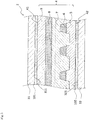
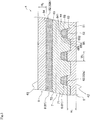
- FIG. 3 is a cross-sectional view illustrating a conductor-layer-equipped structure according to an embodiment of the present invention.
- the conductor-layer-equipped structure 2 comprises a cover glass 31, a liquid crystal panel 32, the wiring body 4, a first adhesion layer 101, and a second adhesion layer 102.
- the "conductor-layer-equipped structure 2" in the present embodiment corresponds to an example of the “conductor-layer-equipped structure” and "touch panel” in the present invention.
- the cover glass 31 is a protection layer that protects components, such as the wiring body 4 and image display device, in the input device 1 from external.
- a cover glass 31 may be, for example, but is not limited to being, composed of appropriate glass, such as soda-lime glass and borosilicate glass.
- the cover glass 31 may be substituted by a transparent resin, such as polymethylmethacrylate (PMMA), which is used as a protection layer that protects the wiring body 4 and the image display device from external.
- PMMA polymethylmethacrylate
- the cover glass 31 is a plate-like member having a uniform thickness.
- the cover glass 31 has a main surface 311 that is formed to be substantially flat.
- the cover glass 31 is provided at the side of one main surface 41 of the wiring body 4 via the first adhesion layer 101.
- the cover glass 31 covers the entire main surface 41 of the wiring body 4, so that the main surface 41 of the wiring body 4 is not exposed to external.
- the first adhesion layer 101 is used to attach the wiring body 4 to the cover glass 31.
- a known adhesive such as an acrylic resin-based adhesive, urethane resin-based adhesive, and polyester resin-based adhesive, can be used for the first adhesion layer 101. From the viewpoint of suppressing the deterioration in visibility of the wiring body 4, it is preferred to use a material having a refractive index of 1.47 or more and 1.52 or less as the material which constitutes the first adhesion layer 101.
- the first adhesion layer 101 is interposed between the cover glass 31 and the wiring body 4.
- the first adhesion layer 101 adheres directly to the main surface 311 of the cover glass 31 and also adheres directly to the main surface 41 of the wiring body 4 (specifically, a third resin layer 9). Only the first adhesion layer 101 is interposed between the cover glass 31 and the wiring body 4 and other configuration, such as a base material, is not interposed therebetween.
- the cover glass 31 and the first adhesion layer 101 are located at the side of a second resin layer 7 with respect to a first resin layer 5.
- relatively smooth surfaces of outer shapes of first and second conductor lines 62 and 82 that constitute the first and second mesh-like electrode layers 61 and 81 are arranged to face the cover glass 31 side. This can suppress the occurrence of scattering or the like of incident light from the cover glass 31 side. Details will be described later.
- the "first adhesion layer 101" in the present embodiment corresponds to an example of the “first adhesion layer” in the present invention.
- the liquid crystal panel 32 is a plate-like member that constitutes the image display device incorporated in the input device 1.
- the liquid crystal panel 32 is provided at the other main surface 42 side of the wiring body 4 via the second adhesion layer 102.
- the liquid crystal panel 32 covers the main surface 42 of the wiring body 4, so that the main surface 42 of the wiring body 4 is not exposed to external.
- the second adhesion layer 102 is used to attach the liquid crystal panel 32 to the wiring body 4.
- the same adhesive as used for the above-described first adhesion layer 101 can be used for the second adhesion layer 102.
- the second adhesion layer 102 is interposed between the liquid crystal panel 32 and the wiring body 4.
- the second adhesion layer 102 adheres directly to a main surface 321 of the liquid crystal panel 32 and also adheres directly to the main surface 42 of the wiring body 4 (specifically, the first resin layer 5). Only the second adhesion layer 102 is interposed between the liquid crystal panel 32 and the wiring body 4 and other configuration, such as a base material, is not interposed therebetween.
- the "second adhesion layer 102" in the present embodiment corresponds to an example of the "second adhesion layer” in the present invention.
- the wiring body 4 is supported by at least one of the cover glass 31 and the liquid crystal panel 32.
- one of the cover glass 31 and the liquid crystal panel 32 is constituted as a support body while the other is constituted as a board.
- both the cover glass 31 and the liquid crystal panel 32 adhere to the wiring body 4 via the adhesion layers, either the cover glass 31 or the liquid crystal panel 32 which adheres to the wiring body 4 via an adhesion layer having larger adhesion strength of the first adhesion layer 101 and the second adhesion layer 102 constitutes the support body.
- the "cover glass 31" in the present embodiment corresponds to an example of one of the “support body” and “board” in the present invention and the “liquid crystal panel 32" in the present embodiment corresponds to an example of the other of the "support body” and "board” in the present invention.
- the present invention is not limited to this, and any component, such as a polarization plate and a color filter, which constitutes the image display device may be used as the support body.
- any component such as a polarization plate and a color filter, which constitutes the image display device may be used as the support body.
- the input device 1 has a hard coat layer, antistatic layer, antidazzle layer, antifouling layer, antireflection layer, high-dielectric layer, and/or electromagnetic shielding layer, any of these may be used as the support body.
- the input device 1 includes an appropriate structure, such as a printed board, heat dissipating plate, and housing, any of these may be used as the support body. That is, the configuration of the support body is not particularly limited, provided that the support body can support the wiring body 4.
- FIG. 4 is a transparent plan view illustrating a wiring body according to an embodiment of the present invention
- FIG. 5 is a cross-sectional view along line V-V of FIG. 4
- FIG. 6 is a cross-sectional view along line VI-VI of FIG. 4
- FIG. 7 is a cross-sectional view for describing a first conductor line according to an embodiment of the present invention.
- FIG. 4 is illustrated with solid lines for a second conductor layer 8 and broken lines for a first conductor layer 6.
- the wiring body 4 comprises the first resin layer 5, the first conductor layer 6, the second resin layer 7, the second conductor layer 8, and the third resin layer 9.
- the wiring body 4 of the present embodiment which is supported by at least one of the cover glass 31 and the liquid crystal panel 32, has a configuration that does not require an additional component, such as a base material, which supports the first and second conductor layers 6 and 8 by direct adhesion.
- the second conductor layer 8 has a similar configuration to that of the first conductor layer 6. In the following description, therefore, detailed description of the second conductor layer 8 (including elements of the second conductor layer 8) will be omitted.
- the "wiring body 4" in the present embodiment corresponds to an example of the "wiring body" in the present invention.
- the first resin layer 5 of the present embodiment is composed of a material having optical isotropy.
- the material which constitutes such a first resin layer 5 include a UV curable resin, such as an epoxy resin, acrylic resin, urethane resin, silicone resin, and phenol resin, and a thermoset resin.
- the material which constitutes the first resin layer 5 has a retardation value Re of 10 nm or less.
- the retardation value Re is preferably 5 nm or less and more preferably 1 nm or less.
- a material having optical isotropy refers to a material of which the retardation value Re is 10 nm or less.
- retardation is a phenomenon in which light incident on an anisotropic substance such as a crystal is split into two light waves having directions of vibration orthogonal to each other. That is, when unpolarized light is incident on a birefringent material, the incident light is split into two light rays: an ordinary ray and an extraordinary ray, and their directions of vibration are orthogonal to each other.
- the extraordinary ray is a light ray of which the propagation speed differs depending on the propagation direction while the ordinary ray is a light ray of which the propagation speed is independent of the propagation direction.
- nx represents a refractive index in a direction (slow axis direction) in which the refractive index is largest in the plane of a resin layer (i.e. extraordinary refractive index)
- ny represents a refractive index in a direction (fast axis direction) that is orthogonal to the slow axis direction (i.e. ordinary refractive index)
- d represents a thickness of the resin layer.
- Such a retardation value can be measured in accordance with a JIS method (JIS K7142).
- the retardation value Re is measured using a known measurement apparatus as a retardation value to light of a wavelength of 550 nm, but the wavelength for measurement is not particularly limited to this.
- the retardation value Re preferably satisfies the above-described condition across the entire wavelength range of visible light.
- N 1 represents a refractive index of the material which constitutes the first resin layer 5.
- Such a refractive index can be measured in accordance with a JIS method (JIS K7142).
- the refractive index N 1 is more preferably 1.47 or more and 1.52 or less (1.47 ⁇ N 1 ⁇ 1.52).
- T 1 represents a total light transmittance of the material which constitutes the first resin layer 5.
- Such a total light transmittance can be measured in accordance with a JIS method (JIS K7375).
- the total light transmittance T 1 is more preferably 99% or more (99% ⁇ T 1 ).
- the material which constitutes the first resin layer 5 is preferably a material having a small volume contraction in the process of forming the first resin layer 5.
- the material which constitutes the first resin layer 5 is preferably a UV-curable resin that does not require a solvent during the process of coating with the material.
- the first resin layer 5 is constituted of a flat part 51 that is provided to have an approximately constant thickness and support parts 52 that are formed on the flat part 51.
- the support parts 52 are formed between the flat part 51 and the first conductor layer 6 so as to protrude toward a direction departing from the flat part 51 (upward direction in FIG. 5 ).
- the first resin layer 5 is in contact with the first conductor layer 6 at upper surfaces of the support parts 52 (surfaces of the support parts 52 at the upper side in FIG. 5 ).
- Each support part 52 has two linear side surfaces that incline so as to come close to each other in a transverse cross-sectional view as departing from the flat part 51.
- the transverse cross-sectional view refers to a cross section along the transverse direction of a first conductor line 62 (described later) that constitutes each first mesh-like electrode layer 61 in contact with the support parts 52.
- Boundaries between the support parts 52 and the first conductor layer 6 are in uneven (irregular) shapes that correspond to uneven shapes of contact surfaces of the first conductor layer 6 (such as contact surfaces 63 of first conductor lines 62 (which will be described later)). Such uneven shapes are formed due to the surface roughness of the contact surfaces of the first conductor layer 6. As illustrated in FIG. 6 , boundaries between the support parts 52 and the first conductor layer 6 in a cross-section along the extending direction of the first conductor layer 6 are also in uneven shapes that correspond to the uneven shapes of adhesion surfaces of the first conductor layer 6. The surface roughness of contact surfaces of the first conductor layer 6 will be described later in detail with reference to an example of the surface roughness of contact surfaces 63 of first conductor lines 62. For easy understanding of the wiring body 4 in the present embodiment, FIG. 5 and FIG. 6 illustrate the uneven shapes of boundaries between the support parts 52 and the first conductor layer 6 in an exaggerated manner.
- H 1 represents a height of the first resin layer 5.
- the height H 1 of the first resin layer 5 refers to a total thickness (height) obtained by summing up the thickness (height) of the flat part 51 which constitutes the first resin layer 5 and the thickness (height) of the support parts.
- the material which constitutes the first resin layer 5 of the present embodiment is a crosslinked resin material.
- the coefficient of thermal expansion of the first resin layer 5 can therefore be reduced as compared with a state before crosslinking the material which constitutes the first resin layer 5.
- the strength and hardness of the first resin layer 5 can be enhanced as compared with the state before crosslinking the material which constitutes the first resin layer 5.
- the shape of the first resin layer 5 can easily be maintained because the first resin layer 5 becomes difficult to dissolve in an organic solvent.
- Such a crosslinked resin material has a characteristic that the modulus of elasticity decreases below a certain temperature as the temperature increases, but under a relatively higher temperature than the certain temperature, the modulus of elasticity rather increases. As is known in the art, the modulus of a material that is not crosslinked continues to decrease monotonically as the temperature increases.
- the crosslink density of the resin material can be expressed using a molecular weight between crosslinks of the resin material.
- Mc represents a molecular weight between crosslinks
- ⁇ represents a Poisson's ratio
- ⁇ represents a density
- R represents a gas constant
- T represents an absolute temperature
- E represents a modulus of elasticity.
- the molecular weight between crosslinks of the material which constitutes the first resin layer 5 is preferably less than 10,000 g/mol and more preferably less than 3,000 g/mol.
- the molecular weight between crosslinks of the material which constitutes the first resin layer 5 is preferably less than 250 times and more preferably less than 80 times the monomer molecular weight.
- the molecular weight between crosslinks of the material which constitutes the first resin layer 5 is preferably 1,000 g/mol or more.
- the "first resin layer 5" in the present embodiment corresponds to an example of the "first resin layer” in the present invention.
- the first conductor layer 6 includes the first mesh-like electrode layers 61 and the lead wires 66.
- the first mesh-like electrode layers 61 are detection electrodes of the input device 1, which extend in the Y-direction as illustrated in FIG. 4 .
- the first mesh-like electrode layers 61 are laid on the support parts 52 of the first resin layer 5 and formed so as to protrude toward the +Z-direction (see FIG. 5 and FIG. 6 ).
- the "first conductor layer 6" in the present embodiment corresponds to an example of the "first conductor layer” in the present invention.
- the first mesh-like electrode layers 61 are constituted of a conductive powder and a binder resin.
- the conductive powder exists to be approximately uniformly dispersed in the binder resin, and particles of the conductive power are in contact with one another thereby to allow the first mesh-like electrode layers 61 to have conductivity.
- Such first mesh-like electrode layers 61 are formed by applying a conductive paste and curing it.
- a conductive paste include a conductive paste that is constituted by mixing water or a solvent and various additives to the above-described conductive powder and binder resin.
- Examples of a material of the conductive powder include a metal material, such as silver, copper, nickel, tin, bismuth, zinc, indium, and palladium, and a carbon-based material, such as graphite, carbon black (furnace black, acetylene black, Ketjen black), carbon nanotube, and carbon nanofiber.
- a metal material such as silver, copper, nickel, tin, bismuth, zinc, indium, and palladium
- a carbon-based material such as graphite, carbon black (furnace black, acetylene black, Ketjen black), carbon nanotube, and carbon nanofiber.
- Metal salts that are salts of the above-described metal materials may also be used, other than the conductive powder.
- Conductive powder that can be used as the conductive powder may have a size ⁇ of 0.5 ⁇ m or more and 2 ⁇ m or less (0.5 ⁇ 2), for example, in accordance with the widths of the first mesh-like electrode layers 61 to be formed (e.g. first conductor lines 62). From the viewpoint of stabilizing the electric resistance value of the first mesh-like electrode layers 61, it is preferred to use conductive powder having an average size ⁇ that is not larger than half the widths of the first mesh-like electrode layers 61 to be formed. When a carbon-based material is used as the conductive powder, it is preferred to use particles of which the specific surface area as measured by the BET method is 20 m 2 /g or more.
- the first mesh-like electrode layers 61 are required to have a relatively small electric resistance value that is not larger than a certain level, it is preferred to use a metal material as the conductive material, while when the first mesh-like electrode layers 61 are accepted to have a relatively large electric resistance value that is not smaller than a certain level, a carbon-based material can be used as the conductive material. From the viewpoint of improving the haze and total light reflectance of a mesh film, it is preferred to use a carbon-based material as the conductive powder.
- binder examples include acrylic resin, polyester resin, epoxy resin, vinyl resin, urethane resin, phenol resin, and polyimide resin.
- solvent examples include ⁇ -terpineol, butyl carbitol acetate, butyl carbitol, 1-decanol, butyl cellosolve, diethylene glycol monoethyl ether acetate, and tetradecane.
- the binder resin may be omitted from the material which constitutes the first mesh-like electrode layers 61.
- each of the first mesh-like electrode layers 61 is configured such that a plurality of first conductor lines 62a and 62b having conductivity intersects with one another, and has a shape as a whole in which a plurality of quadrangle-shaped meshes is arranged to repeat.
- the "first conductor lines 62a and 62b" in the present embodiment correspond to an example of the "first conductor line” in the present invention.
- the "first conductor lines 62a" and the “first conductor lines 62b" may be collectively referred to as “first conductor lines 62," as necessary.
- each outer shape of the first conductor lines 62 of the present embodiment is constituted of a contact surface 63, a top surface 64, and two side surfaces 65 and 65.
- the contact surface 63 is a surface that is in contact with the first resin layer 5.
- the first mesh-like electrode layers 61 of the present embodiment are supported by the first resin layer 5, in which case the contact surface 63 is a surface that is located at the first resin layer 5 side with respect to the top surface 64.
- the contact surface 63 is an uneven surface with fine irregularities in the transverse cross section.
- the top surface 64 is a surface opposite to the contact surface 63 and is substantially in parallel to the lower surface (surface at the lower side in FIG. 5 ) of the first resin layer 5.
- the top surface 64 includes a flat part 641 in the cross-section of the first conductor line 62 in its width direction.
- the flat part 641 is a linear portion (i.e. portion with a considerably large radius of curvature) that exists on the top surface 64 in the cross-section of the first conductor line 62 in its width direction, and the flatness of the flat part 641 is 0.5 ⁇ m or less.
- the flatness can be measured in accordance with a JIS method (JIS B0621 (1984)).
- the flatness of the flat part 641 is obtained using a contactless-type measurement method with laser light.
- a measuring object (the top surface 64 in the present embodiment) is irradiated with strip-like laser light and the reflected light is focused on an imaging element (e.g. two-dimensional CMOS) to measure the flatness.
- the method of calculating the flatness may be a method that includes setting flat surfaces on an object surface so as to pass through three points separate from one another as much as possible and calculating the maximum value of deviation as the flatness (maximum deviation-type flatness).
- the methods of measuring and calculating the flatness are not particularly limited to the above.
- the method of measuring the flatness may be a contact-type measurement method using a dial gauge or other appropriate gauge.
- the method of calculating the flatness may also be a method that includes interposing an object surface between parallel flat surfaces and calculating a value of space generated due to the interposition as the flatness (maximum slope-type flatness).
- the flat part 641 of the present embodiment is formed at approximately the entire area of the top surface 64.
- the location at which the flat part 641 is formed is not particularly limited to the above and the flat part 641 may be formed at a part of the top surface 64.
- the flat part may be formed at a region that does not include both ends of the top surface.
- the width of the flat part may be at least 1/2 or more of the width of the top surface.
- the side surfaces 65 and 65 are linear surfaces that incline so as to come close to each other in the transverse cross-sectional view as departing from the first resin layer 5.
- the side surfaces 65 and 65 are continuous with the support part 52 to be contacted of the first resin layer 5 in the transverse cross-sectional view.
- Each side surface 65 is located between the top surface 64 and the contact surface 63.
- the side surface 65 connects to the top surface 64 at a first portion 651 and connects to the contact surface 63 at a second portion 652.
- the first conductor line 62 of the present embodiment has a tapered shape that narrows toward the second conductor layer 8 side and, therefore, the second portion 652 is located outside the first portion 651.
- the side surface 65 of the present embodiment represents a linear surface that extends on a virtual straight line (not illustrated) passing through the first and second portions 651 and 652.
- the shape of the side surface 65 is not particularly limited to the above.
- the side surface 65 may protrude outside the virtual straight line passing through the first and second portions 651 and 652.
- the side surface 65 is preferably in a shape that is not depressed inside the virtual straight line passing through the first and second portions 651 and 652 in the cross-section of the first conductor line 62 in its width direction (i.e. in a shape in which the lower part of the conductor pattern does not widen in a divergent fashion).
- the side surface 65 of the present embodiment includes a flat part 653 in the cross-section of the first conductor line 62 in its width direction.
- the flat part 653 is a linear portion (i.e. portion with a considerably large radius of curvature) that exists on the side surface 65 in the cross-section of the first conductor line 62 in its width direction, and the flatness of the flat part 653 is 0.5 ⁇ m or less.
- the flat part 653 is formed at approximately the entire area of the side surface 65.
- the shape of the flat part 653 is not particularly limited to the above and the flat part 653 may be formed at a part of the side surface 65.
- an angle ⁇ 1 between the side surface 65 and the top surface 64 is preferably 90° to 170° (90° ⁇ 1 ⁇ 170°) and more preferably 90° to 120° (90° ⁇ 1 ⁇ 120°).
- the angle between one side surface 65 and the top surface 64 is substantially the same as the angle between the other side surface 65 and the top surface 64.
- the surface roughness of the contact surface 63 of the first mesh-like electrode layer 61 in the present embodiment is preferably relatively rougher than the surface roughness of the top surface 64. Since the top surface 64 includes the flat surface 641 in the present embodiment, the above relative relationship of the surface roughness in the first conductor line 62 (relationship that the surface roughness of the contact surface 63 is relatively rougher than the surface roughness of the top surface 64) is established. Specifically, the surface roughness Ra of the contact surface 63 is preferably about 0.1 ⁇ m to 3.0 ⁇ m while the surface roughness Ra of the top surface 64 is preferably about 0.001 ⁇ m to 1.0 ⁇ m.
- the surface roughness Ra of the contact surface 63 of the first conductor line 62 is more preferably 0.1 ⁇ m to 0.5 ⁇ m and the surface roughness Ra of the top surface 64 is furthermore preferably 0.001 ⁇ m to 0.3 ⁇ m.
- the ratio of the surface roughness of the top surface 64 and the surface roughness of the contact surface 63 is preferably 0.01 or more and less than 1 and more preferably 0.1 or more and less than 1.
- the surface roughness of the top surface 64 is preferably 1/5 or less of the width (maximum width) of the first conductor line 62. Such surface roughness can be measured in accordance with a JIS method (JIS B0601 (revised on March 21, 2013)).
- the “surface roughness Ra” refers to "arithmetic average roughness Ra” as described in the JIS method (JIS B0601 (revised on March 21, 2013)).
- the “calculated average roughness Ra” represents a roughness parameter that is obtained by filtering out long-wavelength components (waviness components) from a profile curve. Separation of the waviness components from the profile curve may be performed on the basis of the measurement condition which is necessary for obtaining a form (such as the size of an object, for example).
- the side surface 65 includes the flat part 653.
- the surface roughness of the contact surface 63 is therefore relatively rougher than that of the side surface 65.
- the surface roughness Ra of the contact surface 63 of the first conductor line 62 is preferably 0.1 ⁇ m to 3 ⁇ m while the surface roughness Ra of the side surface 65 is preferably 0.001 ⁇ m to 1.0 ⁇ m.
- the surface roughness of the contact surface 63 is relatively rougher than the surface roughness of the top surface 64 and side surfaces 65 and, therefore, the diffuse reflectance of the wiring body 4 at other surfaces than the contact surface 63 (i.e. at the top surface 64 and side surfaces 65) is relatively smaller than the diffuse reflectance of the wiring body 4 at the contact surface 63.
- the ratio of the diffuse reflectance of the wiring body 4 at other surfaces than the contact surface 63 and the diffuse reflectance of the wiring body 4 at the contact surface 63 is preferably 0.1 or more and less than 1 and more preferably 0.3 or more and less than 1.
- first conductor line 62B having the above-described relative relationship of the surface roughness between the contact surface and other surfaces than the contact surface will be described with reference to FIG. 7 .
- the first electrode line 62B which is constituted by conductive powder particles M and a binder resin B, a number of the conductive powder particles M are dispersed in the binder resin B.
- the first conductor line 62B is formed with a contact surface 63B having an uneven shape in which a part of the conductive powder particles M protrudes from the binder resin B in the cross-section in the width direction and a top surface 64B and side surfaces 65B each having a smooth shape in which the binder resin B gets into spaces between the conductive powder particles M to cover the conductive powder particles M.
- the conductive powder particles M are covered with the binder resin B, so that the electric insulation is improved between adjacent first conductor lines 62B and the occurrence of migration is suppressed.
- the surface roughness of the contact surface 63B is relatively large because a part of the conductive powder particles M protrudes from the binder resin B.
- the surface roughness of the top surface 64B is relatively small because the conductive powder particles M are covered by the binder resin B at the top surface 64B.
- the surface roughness of the contact surface 63B is relatively rougher than the surface roughness of the top surface 64B.
- the surface roughness of the side surface 65B is relatively small because the conductive powder particles M are covered by the binder resin B at the side surface 65B.
- the surface roughness of the contact surface 63B is relatively rougher than the surface roughness of the side surface 65B.
- the "contact surface 63" in the present embodiment corresponds to an example of the "first surface” in the present invention
- the “top surface 64" in the present embodiment corresponds to an example of the “second surface” in the present invention
- the "side surfaces 65 and 65” in the present embodiment correspond to an example of the "side surface” in the present invention.
- each first conductor line 62a extends linearly along a direction inclined by +45° with respect to the X-direction (this direction will be also simply referred to as a "first direction,” hereinafter), and the plurality of the first conductor lines 62a is arranged at a regular pitch P 1 in a direction that is substantially orthogonal to the first direction (this direction will be also simply referred to as a "second direction,” hereinafter).
- each first conductor line 62b extends linearly along the second direction, and the plurality of the first conductor lines 62b is arranged at a regular pitch P 2 in the first direction.
- the first conductor lines 62a and 62b are orthogonal to one another and the first mesh-like electrode layers 61 are thereby formed in which quadrangle-shaped meshes (rhombus-shaped meshes) are arranged to repeat.
- the pitch refers to a center-to-center distance.
- the structure of the first mesh-like electrode layers 61 is not particularly limited to the above.
- the first direction, along which the first conductor lines 62a extend, is a direction inclined by +45° with respect to the X-direction while the second direction, along which the first conductor lines 62b extend, is a direction that is substantially orthogonal to the first direction, but the extending directions of the first and second directions (i.e. an angle of the first direction with respect to the X-axis and an angle of the second direction with respect to the X-axis) can be freely set.
- the mesh shape of the first mesh-like electrode layers 61 may have a certain geometrical pattern. That is, the mesh shape may be a triangle, such as a regular triangle, isosceles triangle and right triangle, and may also be a quadrangle, such as a rectangle, square, rhombus, parallelogram and trapezoid.
- the mesh shape may also be an n-sided polygon, such as a hexagon, octagon, dodecagon and icosagon, circle, ellipsoid, and star-shape.
- the first conductor lines 62 are in a linear form, but the present invention is not particularly limited to this, and they may be in a specific form, such as a curved form, horseshoe-like form and zigzag form.
- the first conductor lines 62a and 62b have approximately the same line width, but may also have different line widths.
- the width W 1 (see FIG. 5 ) of the first conductor lines 62a and 62b is preferably 50 nm to 1,000 ⁇ m, more preferably 500 nm to 150 ⁇ m, further preferably 1 ⁇ m to 10 ⁇ m, and furthermore preferably 1 ⁇ m to 5 ⁇ m.
- the lead wires 66 are provided to correspond to the first mesh-like electrode layers 61.
- three lead wires 66 are formed for the three first mesh-like electrode layers 61.
- the lead wires 66 are led out from the -Y-direction side in the figure of the first mesh-like electrode layers 61 via lead parts 67.
- the lead wires 66 are formed integrally with respective first mesh-like electrode layers 61 using the same material as that of the first mesh-like electrode layers 61 described above.
- the term "integrally with” refers to a situation in which a member and another member are not separated from each other and they are formed as a one-body structure using the same material (such as using conductive powder of the same particle size and the same binder resin).
- locations at which the lead wires 66 are provided are not particularly limited.
- the lead wires 66 are connected to the first mesh-like electrode layers 61 via the lead parts 67, but the present invention is not particularly limited to this, and the lead wires 66 and the first mesh-like electrode layers 61 may also be directly connected.
- the second resin layer 7 is formed on the first resin layer 5 so as to cover the first conductor layer 6.
- the second conductor layer 8 is formed on the second resin layer 7.
- the second resin layer 7 is interposed between the first conductor layer 6 and the second conductor layer 8 and serves to ensure the insulation therebetween.
- the wiring body 4 including the first and second conductor layers 6 and 8 is supported by at least one of the cover glass 31 and the liquid crystal panel 32.
- the second resin layer 7 is merely an insulating material (dielectric material) that is interposed between the first and second conductor layers 6 and 8 (i.e. two electrodes).
- the second resin layer 7 is not required to have rigidity enough to function as a support body that supports electrode layers, which would be necessary in the prior art. It is therefore possible to reduce the thickness (height) of the second resin layer 7, and the wiring body 4 can be made thin accordingly.
- the first resin layer 5 and the second resin layer 7 adhere directly to each other by chemical bond.
- the first and second resin layers 5 and 7 may be bonded to each other due to intermolecular force and/or anchor effect between the resin layers 5 and 7 in addition to the chemical bond.
- the adhesion strength between the first resin layer 5 and the second resin layer 7 in such cases is preferably at least 10 N/cm or more.
- the adhesion strength between the first resin layer 5 and the second resin layer 7 is preferably larger than the breaking strength of the first and second resin layers 5 and 7.
- Examples of the material which constitutes the second resin layer 7 include the same materials as those for constituting the first resin layer 5.
- the wiring body 4 is constituted by selecting the same composition for both the material which constitutes the first resin layer 5 and the material which constitutes the second resin layer 7.
- the second resin layer 7 of the present embodiment is constituted by a material having optical isotropy, thereby to suppress the birefringence for light incident on the wiring body 4.
- the retardation value Re of the material which constitutes the second resin layer 7 is 10 nm or less, preferably 5 nm or less, and more preferably 1 nm or less.
- the material which constitutes the second resin layer 7 is preferably a material having a small volume contraction in the process of forming the second resin layer 7.
- the material which constitutes the second resin layer 7 is preferably a UV-curable resin that does not require a solvent during the process of coating with the material.
- this case is a case in which one or more unit structures that constitute a main chain of the material which constitutes one resin layer (e.g. the first resin layer 5) are all included in a main chain of the material which constitutes the other resin layer (e.g. the second resin layer 7) and one or more unit structures that constitute the main chain of the material which constitutes the other resin layer are all included in the main chain of the material which constitutes the one resin layer.
- one or more substituent groups or functional groups that constitute a side chain of the material which constitutes one resin layer be all included in a side chain of the material which constitutes the other resin layer and one or more substituent groups or functional groups that constitute the side chain of the material which constitutes the other resin layer be all included in the side chain of the material which constitutes the one resin layer.
- the average molecular weight of the material which constitutes one resin layer and the average molecular weight of the material which constitutes the other resin layer be substantially the same.
- one or more substituent groups or functional groups that constitute a side chain of the material which constitutes one resin layer be all included in a side chain of the material which constitutes the other resin layer
- one or more substituent groups or functional groups that constitute the side chain of the material which constitutes the other resin layer be all included in the side chain of the material which constitutes the one resin layer
- the average molecular weight of the material which constitutes one resin layer and the average molecular weight of the material which constitutes the other resin layer be substantially the same.
- the infrared absorption spectrum obtained by infrared spectroscopic analysis for one resin layer and the infrared absorption spectrum obtained by infrared spectroscopic analysis for the other resin layer may be substantially identical.
- N 2 represents a refractive index of the material which constitutes the second resin layer 7 and T 2 represents a total light transmittance of the material which constitutes the second resin layer 7.
- the refractive index N 1 of the material which constitutes the first resin layer 5 and the refractive index N 2 of the material which constitutes the second resin layer 7 are substantially the same because the materials which constitute the first and second resin layers 5 and 7 have the same composition. This can suppress the occurrence of scattering or the like of light incident on the wiring body 4 at the interface between the first and second resin layers 5 and 7. Moreover, the deterioration in visibility of the wiring body 4 can be further suppressed by establishing the above Expressions (12) and (13).
- the situation that the refractive index N 1 of the material which constitutes the first resin layer 5 and the refractive index N 2 of the material which constitutes the second resin layer 7 are substantially the same refers to a case in which the absolute value of the difference between these refractive indices N 1 and N 2 is 0.01 or less.
- the refractive index N 2 is more preferably 1.47 or more and 1.52 or less (1.47 ⁇ N 2 ⁇ 1.52) and the total light transmittance T 2 is more preferably 99% or more (99% ⁇ T 2 ).
- the material which constitutes the second resin layer 7 of the present embodiment is a crosslinked resin material.
- the coefficient of thermal expansion of the second resin layer 7 can therefore be reduced as compared with a state before crosslinking the material which constitutes the second resin layer 7.
- the strength and hardness of the second resin layer 7 can be enhanced as compared with the state before crosslinking the material which constitutes the second resin layer 7.
- the shape of the second resin layer 7 can easily be maintained because the second resin layer 7 becomes difficult to dissolve in an organic solvent.
- the molecular weight between crosslinks of the material which constitutes the second resin layer 7 is preferably less than 10,000 g/mol and more preferably less than 3,000 g/mol.
- the molecular weight between crosslinks of the material which constitutes the second resin layer 7 is preferably less than 250 times and more preferably less than 80 times the monomer molecular weight. From the viewpoint of preventing the second resin layer 7 from being brittle, the molecular weight between crosslinks of the material which constitutes the second resin layer 7 is preferably 1,000 g/mol or more.
- the second resin layer 7 is constituted of a main part 71 that covers the first conductor layer 6 and support parts 72 that are formed on the main part 71.
- the support parts 72 are formed between the main part 71 and the second conductor layer 8 so as to protrude toward a direction departing from the first resin layer 5 (upward direction in FIG. 6 ).
- the rigidity of the second resin layer 7 is enhanced at portions supporting the second conductor layer 8 by forming the support parts 72. Boundaries between the support parts 72 and the second conductor layer 8 are in uneven shapes that correspond to uneven shapes of contact surfaces of the second conductor layer 8 (such as contact surfaces 83 of second conductor lines 82).
- Such uneven shapes are formed due to the surface roughness of the contact surfaces of the second conductor layer 8.
- boundaries between the support parts 72 and the second conductor layer 8 in a cross-section along the extending direction of the second conductor layer 8 are also in uneven shapes that correspond to the uneven shapes of the contact surfaces of the second conductor layer 8.
- the surface roughness of the second conductor layer 8 will be described later in detail with reference to an example of the surface roughness of contact surfaces 83 of second conductor lines 82.
- FIG. 5 and FIG. 6 illustrate the uneven shapes of boundaries between the support parts 72 and the second conductor layer 8 in an exaggerated manner.
- the second resin layer 7 is in contact with the second conductor layer 8 at upper surfaces of the support parts 72 (surfaces of the support parts 72 at the upper side in FIG. 6 ).
- Each support part 72 has two linear side surfaces that incline so as to come close to each other in a transverse cross-sectional view as departing from the first resin layer 5.
- the transverse cross-sectional view refers to a cross section along the transverse direction of a second conductor line 82 (see FIG. 6 ) that constitutes each second mesh-like electrode layer 81 in contact with the support parts 72.
- H 2 represents a height of the second resin layer 7.
- the height H 2 of the second resin layer 7 refers to a thickness (height) of portions of the second resin layer 7 which are interposed between the top surfaces 64 of the first conductor lines 62 and the contact surfaces 83 of the second conductor lines 82.
- the "second resin layer 7" in the present embodiment corresponds to an example of the “second resin layer” in the present invention.
- the second conductor layer 8 like the first conductor layer 6, includes the second mesh-like electrode layers 81 and the lead wires 86.
- the second mesh-like electrode layers 81 are detection electrodes of the input device 1, which extend in the X-direction as illustrated in FIG. 4 .
- the "second conductor layer 8" in the present embodiment corresponds to an example of the "second conductor layer” in the present invention.
- each of the second mesh-like electrode layers 81 is configured such that a plurality of second conductor lines 82a and 82b having conductivity intersects with one another, and has a shape as a whole in which a plurality of quadrangle-shaped meshes is arranged to repeat.
- the "second conductor lines 82a and 82b" in the present embodiment correspond to an example of the "second conductor line” in the present invention.
- the "second conductor lines 82a" and the “second conductor lines 82b” may be collectively referred to as “second conductor lines 82," as necessary.
- each outer shape of the second conductor lines 82 of the present embodiment is constituted of a contact surface 83, a top surface 84, and two side surfaces 85 and 85, as in the first conductor lines 62.
- the contact surface 83 is a surface that is in contact with the second resin layer 7.
- the top surface 84 is a surface opposite to the contact surface 83.
- the side surfaces 85 and 85 are linear surfaces that incline so as to come close to each other in the transverse cross-sectional view as departing from the second resin layer 7.
- the top surface 84 includes a flat part 841 in the cross-section of the second conductor line 82 its width direction.
- the flat part 841 is a linear portion (i.e. portion with a considerably large radius of curvature) that exists on the top surface 84 in the cross-section of the second conductor line 82 in its width direction, and the flatness of the flat part 841 is 0.5 ⁇ m or less.
- the flat part 841 of the present embodiment is formed at approximately the entire area of the top surface 84.
- the location at which the flat part 841 is formed is not particularly limited to the above and the flat part 841 may be formed at a part of the top surface 84.
- the flat part may be formed at a region that does not include both ends of the top surface.
- the width of the flat part may be at least 1/2 or more of the width of the top surface.
- Each side surface 85 is located between the top surface 84 and the contact surface 83.
- the side surface 85 connects to the top surface 84 at a first portion 851 and connects to the contact surface 83 at a second portion 852.
- the second conductor line 82 of the present embodiment has a tapered shape that narrows toward the side departing from the first conductor layer 6 and, therefore, the second portion 852 is located outside the first portion 851.
- the side surface 85 represents a linear surface that extends on a virtual straight line (not illustrated) passing through the first and second portions 851 and 852.
- the shape of the side surface 85 is not particularly limited to the above.
- the side surface 85 may protrude outside the virtual straight line passing through the first and second portions 851 and 852.
- the side surface 85 is preferably in a shape that is not depressed inside the virtual straight line passing through the first and second portions 851 and 852 in the cross-section of the second conductor line 82 in its width direction (i.e. in a shape in which the lower part of the second conductor line 82 does not widen in a divergent fashion).
- the side surface 85 of the present embodiment includes a flat part 853 in the cross-section of the second conductor line 82 in its width direction.
- the flat part 853 is a linear portion (i.e. portion with a considerably large radius of curvature) that exists on the side surface 85 in the cross-section of the second conductor line 82 in its width direction, and the flatness of the flat part 853 is 0.5 ⁇ m or less.
- the flat part 853 is formed at approximately the entire area of the side surface 85.
- the shape of the flat part 853 is not particularly limited to the above and the flat part 853 may be formed at a part of the side surface 85.
- an angle ⁇ 2 between the side surface 85 and the top surface 84 is preferably 90° to 170° (90° ⁇ 2 ⁇ 170°) and more preferably 90° to 120° (90° ⁇ 2 ⁇ 120°).
- the angle between one side surface 85 and the top surface 84 is substantially the same as the angle between the other side surface 85 and the top surface 84.
- the surface roughness of the contact surface 83 of the second mesh-like electrode layer 81 in the present embodiment is preferably relatively rougher than the surface roughness of the top surface 84. Since the top surface 84 includes the flat surface 841 in the present embodiment, the above relative relationship of the surface roughness in the second conductor line 82 (relationship that the surface roughness of the contact surface 83 is relatively rougher than the surface roughness of the top surface 84) is established. Specific values of the surface roughness of the contact surface 83 and the surface roughness of the top surface 84 are preferably similar to the above-described values of the surface roughness of the contact surface 63 and the surface roughness of the top surface 64.
- the surface roughness Ra of the contact surface 83 of the second conductor line 82 is preferably about 0.1 ⁇ m to 3.0 ⁇ m while the surface roughness Ra of the top surface 84 is preferably about 0.001 ⁇ m to 1.0 ⁇ m.
- the surface roughness Ra of the contact surface 83 of the second conductor line 82 is more preferably 0.1 ⁇ m to 0.5 ⁇ m and the surface roughness Ra of the top surface 84 is furthermore preferably 0.001 ⁇ m to 0.3 ⁇ m.
- the ratio of the surface roughness of the top surface 84 and the surface roughness of the contact surface 83 is preferably 0.01 or more and less than 1 and more preferably 0.1 or more and less than 1.
- the surface roughness of the top surface 84 is preferably 1/5 or less of the width (maximum width) of the second conductor line 82. Measurement of the surface roughness of the upper surface 84 and the contact surface 83 may be performed along the width direction of the second conductor line 82 and may also be performed along the extending direction of the second conductor line 82.
- the side surface 85 includes the flat part 853.
- the surface roughness of the contact surface 83 is therefore relatively rougher than that of the side surface 85.
- the surface roughness Ra of the contact surface 83 of the second conductor line 82 is preferably 0.1 ⁇ m to 3 ⁇ m while the surface roughness Ra of the side surface 85 is preferably 0.001 ⁇ m to 1.0 ⁇ m.
- the surface roughness of the contact surface 83 is relatively rougher than the surface roughness of the top surface 84 and side surfaces 85 and, therefore, the diffuse reflectance of the wiring body 4 at other surfaces than the contact surface 83 (i.e. at the top surface 84 and side surfaces 85) is relatively smaller than the diffuse reflectance of the wiring body 4 at the contact surface 83.
- the ratio of the diffuse reflectance of the wiring body 4 at other surfaces than the contact surface 83 and the diffuse reflectance of the wiring body 4 at the contact surface 83 is preferably 0.1 or more and less than 1 and more preferably 0.3 or more and less than 1 from the viewpoint of improving the visibility of the wiring body 4.
- the shape of the second conductor line having the above-described relative relationship of the surface roughness between the contact surface and other surfaces than the contact surface may be the same as the shape of the first conductor lines 62B illustrated in FIG. 7 .
- the second conductor line is formed with the contact surface having an uneven shape in which a part of the conductive powder particles protrudes from the binder resin in the cross-section in the width direction and the top surface and side surfaces each having a smooth shape in which the binder resin gets into spaces between the conductive powder particles to cover the conductive powder particles.
- the surface roughness of the contact surface is relatively rougher than the surface roughness of the top surface.
- the surface roughness of the contact surface is relatively rougher than the surface roughness of the side surfaces.
- the width and height of the second conductor line 82 can be set within the above-described ranges of the width and height of the first conductor line 62.
- the third resin layer 9 is formed on the second resin layer 7 so as to cover the second conductor layer 8.
- the third resin layer 9 serves as a protection layer that protects the second conductor layer 8 from external. Moreover, when the third resin layer 9 covers the second conductor layer 8, the occurrence of scattering or the like of light at the surface of the wiring body 4 is suppressed and the deterioration in visibility of the wiring body 4 can be further suppressed.
- the material which constitutes the third resin layer 9 has the same composition as that of the material which constitutes the first and second resin layers 5 and 7.
- the third resin layer 9 is constituted by the material having optical isotropy as in the first and second resin layers 5 and 7 and the birefringence for light incident on the wiring body 4 is therefore suppressed.
- the refractive index of the material which constitutes the second resin layer 7 and the refractive index of the material which constitutes the third resin layer 9 are substantially the same and the occurrence of scattering or the like of light incident on the wiring body 4 can thereby be suppressed at the interface between the second and third resin layers 7 and 9.
- H 3 represents a height of the third resin layer 9.
- the height H 3 of the third resin layer 9 refers to a thickness (height) of portions of the third resin layer 9 which are interposed between the top surfaces 84 of the second conductor lines 82 and the surface of the third resin layer 9 opposite to the surface located at the second resin layer 7 side.
- the height H 3 of the third resin layer 9 is preferably 1 ⁇ m or more and 180 ⁇ m or less (1 ⁇ m ⁇ H 3 ⁇ 180 ⁇ m).
- the "third resin layer 9" in the present embodiment corresponds to an example of the "third resin layer” in the present invention.
- FIG. 8(a) to FIG. 8(e) and FIG. 9(a) to FIG. 9(k) are cross-sectional views illustrating a method of manufacturing a conductor-layer-equipped structure according to an embodiment of the present invention.
- a recessed plate 11 is prepared as illustrated in FIG. 8(a) .
- the recessed plate 11 is formed with recesses 111 having shapes that correspond to the shape of the first conductor layer 6.
- Examples of a material that constitutes the recessed plate 11 include nickel, silicon, glasses such as silicon dioxide, organic silicas, glassy carbon, thermoplastic resin, and photo-curable resin.
- the depth of portions of the recesses 111 corresponding to the first mesh-like electrode layers 61 is preferably 100 nm to 100 ⁇ m, further preferably 500 nm to 10 ⁇ m, and furthermore preferably 500 nm to 5 ⁇ m.
- the width of the portions is preferably 100 nm to 100 ⁇ m, further preferably 500 nm to 10 ⁇ m, and furthermore preferably 500 nm to 5 ⁇ m.
- the depth of portions of the recesses 111 corresponding to the lead wires 66 is preferably the same or deeper than that for the first mesh-like electrode layers 61, that is, preferably 100 nm to 500 ⁇ m, further preferably 500 nm to 100 ⁇ m, and furthermore preferably 500 nm to 30 ⁇ m.
- the width of the portions is preferably wider than that for the first mesh-like electrode layers 61, that is, preferably 1 ⁇ m to 500 ⁇ m, further preferably 1 ⁇ m to 100 ⁇ m, and furthermore preferably 1 ⁇ m to 30 ⁇ m.
- the cross-sectional shapes of the recesses 111 are each formed in a tapered shape that narrows toward the bottom part.
- the surfaces of the recesses 111 preliminarily formed with release layers (not illustrated) constituted of an appropriate material, such as a black lead-based material, silicone-based material, fluorine-based material, ceramic-based material, and aluminum-based material.
- the recesses 111 of the above recessed plate 11 are filled with a conductive material 12.
- the conductive paste as described above may be used as such a conductive material 12.
- Examples of a method of filling the recesses 111 of the recessed plate 11 with the conductive material 12 include a dispensing method, ink-jet method, and screen printing method.
- Another possible method may include coating with a conductive material, such as by a slit-coating method, bar-coating method, blade-coating method, dip-coating method, spray-coating method and spin-coating method, and then wiping, scratching, suctioning, peeling, washing, or blowing away the conductive material applied to other parts than the recesses 111.
- An appropriate method can be selected in accordance with the composition or the like of the conductive material and the shape or the like of the recessed plate.
- the conductive material 12 which fills the recesses 111 of the recessed plate 11 is heated to form the first conductor layer 6.
- a heating condition for the conductive material 12 can be appropriately set in accordance with the composition or the like of the conductive material. Due to this heat treatment, the conductive material 12 undergoes volume contraction to slightly form uneven shapes on surfaces 121 of the conductive material 12. During this treatment, outer surfaces other than the upper surfaces of the conductive material 12 are formed into shapes that follow the recesses 111.
- the treatment method for the conductive material 12 is not limited to heating.
- the conductive material 12 may be irradiated with energy rays, such as infrared rays, ultraviolet rays and laser light, or may be simply dried. Two or more treatment methods as the above may be employed in combination.
- the uneven shapes of the surfaces 121 increase the contact area between the first conductor layer 6 and the first resin layer 5 and the first conductor layer 6 can be more tightly fixed to the first resin layer 5.
- a resin material 13 is applied onto the recessed plate 11 formed with the first conductor layer 6 (recessed plate 11 in the state illustrated in FIG. 8(b) ).
- the above-described material which constitutes the first resin layer 5 can be used as such a resin material 13.
- Examples of a method of applying the resin material 13 onto the recessed plate 11 include a screen printing method, spray-coating method, bar-coating method, dip method, ink-jet method, and casting method.
- the viscosity of the resin material 13 may be adjusted and/or various additives may be mixed.
- the resin material 13 may be mixed with some agent, such as a solvent and curing initiator, which is suitable for the curing treatment for the resin material 13.
- some agent such as a solvent and curing initiator, which is suitable for the curing treatment for the resin material 13.
- the characteristics of the first resin layer 5 include the thickness, resistance to ion migration, resistance to ultraviolet, and releasability of the first resin layer 5.
- Adjustment of the viscosity of the resin material 13 may be performed, such as by adjusting the content of a solvent to be mixed and adjusting the molecular weight in the raw material state of a unit structure that constitutes the main chain of the material which constitutes the resin material 13.
- a UV-curable resin that does not require a solvent may preferably be used as the resin material 13 because the volume contraction is small during the process of forming the first resin layer 5.
- a support base material 14 is disposed above the recessed plate 11 and pressed against the recessed plate 11 so that the resin material 13 gets into the recesses 111 of the recessed plate 11, and the resin material 13 is cured.
- the curing treatment for the resin material 13 is performed by generating a chemical reaction (such as a polymerization reaction and crosslinking reaction) in the resin material 13.
- a chemical reaction such as a polymerization reaction and crosslinking reaction
- Examples of the method of curing the resin material 13 include irradiation with energy rays, such as ultraviolet rays, infrared rays and laser light, heating, heating and cooling, and drying.
- the heating method or irradiation method for the resin material 13 is appropriately set in accordance with the characteristics of the first resin layer 5 to be formed.
- the quantity of heat applied to the resin material 13 is appropriately set in accordance with the characteristics of the first resin layer 5 to be formed. The first resin layer 5 is thus formed.
- the support base material 14 is to provisionally support the wiring body 4, such as when conveying the wiring body 4, until the wiring body 4 is supported by at least one of the cover glass 31 and the liquid crystal panel 32.
- An appropriate material such as polyethylene terephthalate (PET), polyolefin film, polyvinyl chloride (PVC), polyethylene (PE), polypropylene (PP), and polystyrene (PS), can be used as the material which constitutes the support base material 14. It suffices that the material which constitutes the support base material 14 has rigidity enough to provisionally support the wiring body 4.
- the material is not particularly limited to the above and it may be possible to employ a more inexpensive material.
- the function of supporting the wiring body 4 (specifically, the first and second conductor layers 6 and 8) is separated from the configuration of the wiring body 4 and it is thus possible to reduce the thickness of the wiring body 4 and suppress the deterioration in visibility due to the retardation value Re of the member which supports the electrode layers (i.e. the support base material 14 in the present embodiment).
- the production cost for the wiring body 4 can be reduced because an inexpensive material can be employed as the material which constitutes the support base material 14.
- N 1 represents peel strength between the first resin layer 5 and the support base material 14.
- the peel strength in the present description can be measured in accordance with a JIS method (JIS Z0237).
- N 1 is preferably 0.2 N/cm or less (0.01 N/cm ⁇ N 1 ⁇ 0.2 N/cm).
- the support base material 14 of the present embodiment is subjected to surface treatment such that a main surface of the support base material 14 at the side facing the main surface 42 of the wiring body 4 can be smooth.
- the surface roughness Ra of the main surface of such a support base material 14 is preferably 0.1 ⁇ m or less and more preferably 0.05 ⁇ m or less.
- the above surface roughness of the support base material 14 can be achieved by removing an additive and/or filler contained in the material which constitutes the support base material 14 and/or by reducing the size of the filler (filler diameter).
- the scheme of achieving the above Expression (19) is not particularly limited to the above and another surface treatment may also be employed, such as performing a coating process of forming a coating layer on the main surface of the support base material 14.
- the material which constitutes the coating layer include a silicone-based material, fluorine-based material, black lead-based material, ceramic-based material, and aluminum-based material.
- the thickness of such a coating layer is preferably 1 ⁇ m or less.
- Examples of a method of forming the coating layer on the main surface of the support base material 14 include a method of applying a coating liquid that contains the above-described material to the main surface of the support base material 14, then drying the coating liquid to cure it, and performing other steps if necessary.
- the method of surface treatment for the support base material 14 is not limited to the above, provided that the above Expression (19) can be achieved. Any known method can be employed.
- the first resin layer 5 can be formed through adding various additives or the like to the resin material 13 to improve the flowability, performing flow casting using the above method, and then heating the resin material 13 thereby to generate a chemical reaction in the resin material 13.
- the method of forming the first resin layer 5 is not limited to the above.
- the first resin layer 5 may be formed through preparing the support base material 14 on which the resin material 13 for forming the first resin layer 5 is approximately uniformly applied and curing the resin material 13 in a state in which the support base material 14 is pressed against the recessed plate 11 so that the resin material 13 gets into the recesses 111 of the recessed plate 11.
- a recessed plate 16 is prepared as illustrated in FIG. 9(a) .
- the recessed plate 16 is formed with recesses 161 having shapes that correspond to the shape of the second conductor layer 8.
- the same material as that for constituting the recessed plate 11 can be exemplified as a material that constitutes the recessed plate 16.
- the shapes of the recesses 161 formed in the recessed plate 16 correspond to the second conductor layer 8, but the depths and widths of the recesses 161 have the same values as those of the above-described recesses 111 because the second conductor layer 8 has a similar configuration to that of the first conductor layer 6.
- the surfaces of the recesses 161, like the recesses 111 to be preliminarily formed with release layers (not illustrated) constituted of an appropriate material, such as a black lead-based material, silicone-based material, fluorine-based material, ceramic-based material, and aluminum-based material.
- the recesses 161 of the above recessed plate 16 are filled with a conductive material 17.
- the same material as that for the conductive material 12 can be exemplified as such a conductive material 17.
- the same method as that for filling the recesses 111 of the recessed plate 11 with the conductive material 12 can be used as a method for filling the recesses 161 of the recessed plate 16 with the conductive material 17.
- the conductive material 17 which fills the recesses 161 of the recessed plate 16 is heated to form the second conductor layer 8.
- a heating condition for the conductive material 17 can be appropriately set in accordance with the composition or the like of the conductive material. Due to this heat treatment, the conductive material 17 undergoes volume contraction to slightly form uneven shapes on surfaces 171 of the conductive material 17. During this treatment, outer surfaces other than the upper surfaces of the conductive material 17 are formed into shapes that follow the recesses 161.
- the uneven shapes of the surfaces 171 increase the contact area between the second conductor layer 8 and the second resin layer 7 and the second conductor layer 8 can be more tightly fixed to the second resin layer 7.
- the treatment method for the conductive material 17 is not limited to heating.
- a resin material 18 is applied onto the first intermediate body 15.
- the above-described material which constitutes the second resin layer 7 can be used as such a resin material 18, but in the present embodiment, a material having the same composition as that of the above-described material selected for the resin material 13 is used.
- the viscosity of the resin material 18 may be adjusted and/or various additives may be mixed.
- the resin material 18 may be mixed with some agent, such as a solvent and curing initiator, which is suitable for the curing treatment for the resin material 18.
- the characteristics of the second resin layer 7 may be the same as those of the first resin layer 5.
- the same method as that of adjusting the viscosity of the resin material 13 can be used as the method of adjusting the viscosity of the resin material 18.
- a UV-curable resin that does not require a solvent may preferably be used as the resin material 18 because the volume contraction is small during the process of forming the second resin layer 7.
- an additive, solvent, and curing initiator mixed in the resin material 13 may be different from an additive, solvent, and curing initiator mixed in the resin material 18.
- the situation that the material which constitutes the first resin layer 5 and the material which constitutes the second resin layer 7 have the same composition is determined in accordance with a state after the first and second resin layers 5 and 7 are formed, regardless of whether the composition of the resin material 13 and the composition of the resin material 18 are different.
- the viscosity of the material which constitutes the second resin layer 7 is preferably 1 mPa ⁇ s to 10,000 mPa ⁇ s.
- the storage elastic modulus of the resin after curing is preferably 10 6 Pa or more and 10 9 Pa or less.
- Examples of a method of applying the resin material 18 onto the first intermediate body 15 include a screen printing method, spray-coating method, bar-coating method, dip method, ink-jet method, and casting method.
- the first resin layer 5 which constitutes the first intermediate body 15 is cured by generating a chemical reaction in the resin material 13.
- the resin material 13 and the material which constitutes the first resin layer 5 therefore have different main skeletons.
- the molecular weight of the resin material 13 and the molecular weight of the material which constitutes the first resin layer 5 are different.
- the first resin layer 5 is not eroded by the solvent and the like contained in the resin material 18.
- the first resin layer 5 does not deform by heat due to the quantity of heat of the resin material 18.
- the first intermediate body 15 and the recessed plate 16 are disposed on the recessed plate 16 so that the resin material 18 gets into the recesses 161 of the recessed plate 16, the first intermediate body 15 is pressed against the recessed plate 16, and the resin material 18 is cured.
- the pressing pressure when pressing the first intermediate body 15 against the recessed plate 16 is preferably 0.001 MPa to 100 MPa and more preferably 0.01 MPa to 10 MPa.
- the pressing can be performed, such as using pressure rollers.
- the second resin layer 7 is formed, and the first intermediate body 15 and the second conductor layer 8 adhere to and are fixed to each other via the second resin layer 7.
- the curing treatment for the resin material 18 is performed by generating a chemical reaction in the resin material 18.
- Examples of the method of curing the resin material 18 include irradiation with energy rays, such as ultraviolet rays, infrared rays and laser light, heating, heating and cooling, and drying.
- the second resin layer 7 is thus formed.
- orientation of molecules does not occur because physical pressure is not applied to the second resin layer 7 when forming it. This allows the second resin layer 7 to have optical isotropy, and the deterioration in visibility of the wiring body 4 including the second resin layer 7 is suppressed.
- a chemical reaction occurs between the resin material 18 and functional groups of the material which constitutes the first resin layer 5 during the process of pressing the first intermediate body 15 against the resin material 18 and curing the resin material 18.
- the first resin layer 5 and the second resin layer 7 are therefore brought into a state of being chemically bonded together.
- the first resin layer 5 and the second resin layer 7 may also be bonded to each other due to intermolecular force and/or anchor effect between the resin layers 5 and 7 in addition to the above-described chemical bond.
- a resin material 20 is applied onto the second intermediate body 19.
- the above-described material which constitutes the third resin layer 9 can be used as such a resin material 20, but in the present embodiment, a material having the same composition as that of the above-described material selected for the resin materials 13 and 18 is used.
- the viscosity of the resin material 20 may be adjusted and/or various additives may be mixed.
- the resin material 20 may be mixed with some agent, such as a solvent and curing initiator, which is suitable for the curing treatment for the resin material 20.
- the characteristics of the third resin layer 9 may be the same as those of the first resin layer 5.
- the same method as that of adjusting the viscosity of the resin material 13 can be used as the method of adjusting the viscosity of the resin material 20.
- a UV-curable resin that does not require a solvent may preferably be used as the resin material 20 because the volume contraction is small during the process of forming the third resin layer 9.
- Additives, solvents, curing initiators, and the like to be mixed may be different between the resin materials 13 and 18 and the resin material 20.
- the situation that the material which constitutes the first resin layer 5 or the material which constitutes the second resin layer 7 and the material which constitutes the third resin layer 9 have the same composition is determined in accordance with a state after the first to third resin layers 5, 7, and 9 are formed, regardless of whether the composition of the resin materials 13 and 18 and the composition of the resin material 20 are different.
- the viscosity of the material which constitutes the third resin layer 9 is preferably 1 mPa ⁇ s to 10,000 mPa ⁇ s.
- the storage elastic modulus of the resin after curing is preferably 10 6 Pa or more and 10 9 Pa or less.
- Examples of a method of applying the resin material 20 onto the second intermediate body 19 include a screen printing method, spray-coating method, bar-coating method, dip method, ink-jet method, and casting method.
- the second resin layer 7 which constitutes the second intermediate body 19 is cured by generating a chemical reaction in the resin material 18.
- the resin material 18 and the material which constitutes the second resin layer 7 therefore have different main skeletons.
- the molecular weight of the resin material 18 and the molecular weight of the material which constitutes the second resin layer 7 are different.
- the second resin layer 7 is not eroded by the solvent and the like contained in the resin material 20.
- the second resin layer 7 does not deform by heat due to the quantity of heat of the resin material 20.
- the resin material 20 is cured to form the third resin layer 9.
- the curing treatment for the resin material 20 is performed by generating a chemical reaction in the resin material 20.
- the method of curing the resin material 20 include irradiation with energy rays, such as ultraviolet rays, infrared rays and laser light, heating, heating and cooling, and drying.
- energy rays such as ultraviolet rays, infrared rays and laser light
- heating, heating and cooling, and drying orientation of molecules does not occur because physical pressure is not applied to the third resin layer 9 when forming it. This allows the third resin layer 9 to have optical isotropy, and the deterioration in visibility of the wiring body 4 including the third resin layer 9 is suppressed.
- an adhesive material 21 that constitutes the first adhesion layer 101 is applied onto the cover glass 31.
- an adhesive material 21 include an acrylic resin, urethane resin, and polyester resin.
- Examples of a method of applying the adhesive material 21 onto the cover glass 31 include a screen printing method, spray-coating method, bar-coating method, dip method, ink-jet method, and casting method.
- the second intermediate body 19 is pressed against the cover glass 31 in a state in which the adhesive material 21 is interposed between the second intermediate body 19 and the cover glass 31, and the adhesive material 21 is cured.
- the method of curing the adhesive material 21 include irradiation with energy rays, such as ultraviolet rays, infrared rays and laser light, heating, heating and cooling, and drying.
- the first adhesion layer 101 is thus formed.
- the cover glass 31 adheres to the main surface 41 of the wiring body 4 via the first adhesion layer 101.
- the wiring body 4 is supported by the cover glass 31 from the main surface 41 side.
- the support base material 14 is removed to expose the main surface 42 of the wiring body 4 (first resin layer 5). Even when the support base material 14 is removed from the wiring body 4, the possibility of damage of the wiring body 4 is low because the wiring body 4 is supported by the cover glass 31 via the first adhesion layer 101.
- the timing of removing the support base material 14 is not particularly limited to the above.
- the support base material 14 may be removed after the third resin layer 9 is formed ( FIG. 9(f) ). In this case, the support base material 14 is removed before the cover glass 31 is provided on the main surface 41 of the wiring body 4.
- an adhesive material 22 that constitutes the second adhesion layer 102 is applied onto the main surface 321 of the liquid crystal panel 32.
- the same material as the above-described adhesive material 21 may be used as such an adhesive material 22.
- the same method as that of applying the above-described adhesive material 21 onto the cover glass 31 may be used as the method of applying the adhesive material 22 onto the liquid crystal panel 32.
- the second intermediate body 19 is pressed against the liquid crystal panel 32 in a state in which the adhesive material 22 is interposed between the second intermediate body 19 and the liquid crystal panel 32, and the adhesive material 22 is cured.
- the same method as that of curing the above-described adhesive material 21 may be used as the method of curing the adhesive material 22.
- the second adhesion layer 102 is thus formed.
- the liquid crystal panel 32 is provided on the main surface 42 of the wiring body 4 via the second adhesion layer 102.
- the conductor-layer-equipped structure 2 can be obtained in the above manner.
- the conductor-layer-equipped structure 2 of the present embodiment has the following effects.
- a touch position detecting mechanism using a capacitance scheme which is constituted of a base material and two electrode layers formed on both main surfaces of the base material.
- the material which constitutes the base material has to be selected so as to ensure the rigidity enough to support the two electrode layers. It is therefore difficult to reduce the thickness (height) of the base material because the base material has to support the two electrode layers. As a result, the touch panel cannot be made thin.
- a material formed by stretching a resin material and thus having birefringence is generally used as such a base material.
- interference color and the like occur on the image display surface of the touch panel due to the phase difference of light transmitting through the base material, and the visibility of the touch panel may deteriorate. It can be considered to suppress the above-described deterioration in visibility by employing a material having optical isotropy and thus having a small retardation value or by employing a material having optical anisotropy and thus having a large retardation value (i.e. a material with large birefringence). When such a material having a small or large retardation value is used, however, the production cost may increase.
- Conventionally-used materials having optical isotropy include cellulose triacetate, polycarbonate, and cycloolefin.
- the two electrode layers which constitute the touch position detecting mechanism are each constituted of an electrode and a resin layer that supports the electrode.
- these materials are preliminarily formed into film-like shapes and the two resin layers have to be bonded together using an adhesive material.
- the materials which constitute the resin layers and the adhesive material therefore have different compositions, and the difference of refractive index between the materials which constitute the resin layers and the adhesive material may cause scattering or the like of incident light to deteriorate the visibility of the tough position detecting mechanism.
- the above-described conventional materials having optical isotropy are not crosslinked and thus have a relatively large coefficient of thermal expansion, and the dimensional accuracy against a temperature change is poor. Moreover, since the above-described conventional materials having optical isotropy are not crosslinked, the strength and hardness of the resin layers constituted of such materials are relatively poor. Furthermore, the above-described conventional materials having optical isotropy are soluble in an organic solvent and, therefore, the material which constitutes one resin layer may erode and/or thermally deform the other resin layer. Thus, the two resin layers cannot be laid on each other.
- the birefringence for light incident on the wiring body 4 is suppressed because the material which constitutes the first resin layer 5 and the material which constitutes the second resin layer 7 have the same composition and thus have optical isotropy. This can suppress the deterioration in visibility of the conductor-layer-equipped structure 2. Moreover, the use of expensive materials is not necessary for the first and second resin layers 5 and 7 and the cost can be reduced.
- the first conductor layer 6 is supported by the first resin layer 5, and a base material or the like for supporting the first conductor layer 6 is therefore not necessary.
- the deterioration in visibility of the conductor-layer-equipped structure 2 can thus be suppressed and the conductor-layer-equipped structure 2 can be made thin.
- the cover glass 31 is provided at one main surface 41 side of the wiring body 4
- the liquid crystal panel 32 is provided at the other main surface 42 side of the wiring body 4
- the wiring body 4 is supported by at least one of the cover glass 31 and the liquid crystal panel 32.
- Only the first adhesion layer 101 is interposed between the cover glass 31 and the one main surface 41 of the wiring body 4, and other configuration such as a base material is not present there.
- only the second adhesion layer 102 is interposed between the liquid crystal panel 32 and the other main surface 42 of the wiring body 4, and other configuration such as a base material is not present there.
- the deterioration in visibility of the conductor-layer-equipped structure 2 can be suppressed and the conductor-layer-equipped structure 2 can be made thin because a base material or the like that adheres directly to the wiring body 4 to support it is not used.
- JP2014-191717A discloses a touch panel in which conductor layers such as a primer layer and sensor electrode are formed on a printing base material (support base material).
- the touch panel cannot be made thin because of having the printing base material.
- the base material having optical isotropy is expensive and disadvantageous in reducing the cost.
- such a printing material is not used in the present embodiment.
- the touch panel can therefore be made thin and the visibility can be improved.
- conductive compositions for obtaining sensor electrodes and the like are cured on the support base material.
- the support base material therefore cannot be cleanly removed from the wiring body because the support base material and the insulating resin are burnt in and/or the support base material deforms.
- the conductor-layer-equipped structure 2 (wiring body 4) cannot be obtained without using the support base material 14.
- the refractive index N1 of the material which constitutes the first resin layer 5 and the refractive index N2 of the material which constitutes the second resin layer 7 are substantially the same because the material which constitutes the first resin layer 5 and the material which constitutes the second resin layer 7 have the same composition. This can suppress the occurrence of scattering or the like of light incident on the wiring body 4 at the interface between the first and second resin layers 5 and 7, and the deterioration in visibility of the conductor-layer-equipped structure 2 can be suppressed.
- the material which constitutes the first resin layer 5 and the material which constitutes the second resin layer 7 have the same composition, and the coefficient of thermal expansion can thereby be substantially the same between these resin layers 5 and 7.
- the degree of change in dimension e.g. amount of change and direction of change
- This can therefore be substantially the same between the first and second resin layers 5 and 7. This can prevent the occurrence of misalignment between the first mesh-like electrode layers 61 located on the first resin layer 5 and the second mesh-like electrode layers 81 located on the second resin layer 7. It is thus possible to suppress the deterioration in visibility of the conductor-layer-equipped structure 2 due to unevenness of overlapping portions between the first and second mesh-like electrode layers 61 and 81 in the plan view.
- the material which constitutes the first resin layer 5 and the material which constitutes the second resin layer 7 have the same composition, when one or more substituent groups or functional groups that constitute a side chain of the material which constitutes the first resin layer 5 are all included in a side chain of the material which constitutes the second resin layer 7 and one or more substituent groups or functional groups that constitute the side chain of the material which constitutes the second resin layer 7 are all included in the side chain of the material which constitutes the first resin layer 5, the refractive index N1 of the material which constitutes the first resin layer 5 and the refractive index N2 of the material which constitutes the second resin layer 7 can be more identical with each other, and the coefficient of thermal expansion of the material which constitutes the first resin layer 5 and the coefficient of thermal expansion of the material which constitutes the second resin layer 7 can also be more identical with each other.
- This can further suppress the occurrence of scattering or the like of light incident on the wiring body 4 at the interface between the first and second resin layers 5 and 7 and can also further suppress the occurrence of unevenness of overlapping portions between the first and second mesh-like electrode layers 61 and 81. As a result, the deterioration in visibility of the conductor-layer-equipped structure 2 can be further suppressed.
- the material which constitutes the first resin layer 5 and the material which constitutes the second resin layer 7 have the same composition, when the average molecular weight of the material which constitutes the first resin layer 5 and the average molecular weight of the material which constitutes the second resin layer 7 are substantially the same, the refractive index N1 of the material which constitutes the first resin layer 5 and the refractive index N2 of the material which constitutes the second resin layer 7 can be more identical with each other, and the coefficient of thermal expansion of the material which constitutes the first resin layer 5 and the coefficient of thermal expansion of the material which constitutes the second resin layer 7 can also be more identical with each other.
- This can further suppress the occurrence of scattering or the like of light incident on the wiring body 4 at the interface between the first and second resin layers 5 and 7 and can also further suppress the occurrence of unevenness of overlapping portions between the first and second mesh-like electrode layers 61 and 81. As a result, the deterioration in visibility of the conductor-layer-equipped structure 2 can be further suppressed.
- curing treatment is performed by generating a chemical reaction in the resin material 13 to form the first resin layer 5.
- the resin material 13 and the material which constitutes the first resin layer 5 have different main skeletons, and the molecular weight of the resin material 13 and the molecular weight of the material which constitutes the first resin layer 5 are different. Accordingly, even though the resin material 18 having the same composition as that of the resin material 13 is applied onto the first intermediate body 15, the first resin layer 5 is not eroded by the solvent and the like contained in the resin material 18. Moreover, the first resin layer 5 does not deform by heat due to the quantity of heat of the resin material 18.
- the above Expressions (8) and (12) are established and it is thus possible to reduce the difference between the refractive index of the material which constitutes the above-described cover glass 31 and the refractive indices of the first and second resin layers 5 and 7.
- the occurrence of scattering or the like of light incident on the conductor-layer-equipped structure 2 can therefore be suppressed. This can suppress the deterioration in visibility of the conductor-layer-equipped structure 2.
- the surface roughness of the contact surfaces 63 and 83 are relatively rougher than the surface roughness of the top surfaces 64 and 84.
- the first mesh-like electrode layers 61 and the first resin layer 5, or the second mesh-like electrode layers 81 and the second resin layer 7, can thus be tightly fixed to each other.
- the material which constitutes the third resin layer 9 has the same composition as that of the material which constitutes the first and second resin layers 5 and 7, and the third resin layer 9 is thus constituted of the material having optical isotropy.
- the birefringence for light incident on the wiring body 4 is therefore suppressed. This can further suppress the deterioration in visibility of the conductor-layer-equipped structure 2.
- the refractive index of the material which constitutes the second resin layer 7 and the refractive index of the material which constitutes the third resin layer 9 are substantially the same, and the occurrence of scattering or the like of light incident on the wiring body 4 can therefore be suppressed at the interface between the second and third resin layers 7 and 9. It is thus possible to suppress the deterioration in visibility of the conductor-layer-equipped structure 2.
- the wiring body 4 satisfies the above Expression (15) and the distance between the first conductor lines 62 and the second conductor lines 82 is thus long.
- the electric characteristics can therefore be prevented from deteriorating and the wiring body 4 can normally function as a wiring body having two or more conductive layers.
- the film thickness of the entire wiring body 4 (input device or wiring board 1) can be thin because the first resin layer 5 is thicker than the second resin layer 7.
- contact with a contact body such as a finger allows the touch sensor to appropriately react to the contact body because the lines of electric force released can be prevented from being closed between the first conductor lines 62 and the second conductor lines 82. This results in improved ability of detection.
- a reduced film thickness of the conductor-layer-equipped structure 2 as a whole can improve the optical transparency.
- the wiring body 4 satisfies the above Expression (16) and the thickness H 2 of the second resin layer 7 can thus be prevented from being unduly thick beyond necessity.
- the film thickness of the conductor-layer-equipped structure 2 as a whole can therefore by made thin.
- the wiring body 4 satisfies the above Expression (17) and the entire film thickness can thus be made thin even when the third resin layer 9 is provided.
- the optical transparency can also be improved.
- the surface roughness i.e. the roughness parameter obtained by shutting off the waviness components
- the surface roughness Ra of the contact surface 63 of the first conductor line 62 is relatively rougher than the surface roughness of other surfaces (surfaces including the top surface 64 and side surfaces 65 of the first conductor line 62). This can suppress the diffuse reflection of incident light from external while allowing the first conductor line 62 and the first resin layer 5 to tightly adhere to each other.
- the width of the conductor line 62 is 1 ⁇ m to 5 ⁇ m, a remarkable effect can be obtained that the relative relationship of the surface roughness between the adhesion surface and other surfaces can satisfy the above-described relationship thereby to suppress the diffuse reflection of incident light from external while allowing the first resin layer 5 and the first conductor line 62 to tightly adhere to each other.
- the side surface 65 extends so as to substantially coincide with the virtual line passing through the first and second portions 651 and 652.
- the side surface is not in a shape that is depressed inside the virtual straight line in the cross-section of the constitutional element of the first conductor layer in its width direction (i.e. not in a shape in which the lower part of the conductor pattern widens in a divergent fashion).
- the diffuse reflection of incident light from external of the conductor-layer-equipped structure 2 is therefore suppressed.
- the visibility of the touch panel or the like can be further improved.
- the surface roughness Ra of the contact surface 63 is relatively rougher than the surface roughness Ra of other surfaces than the contact surface 63 and, accordingly, the diffuse reflectance of the wiring body 4 at the other surfaces is relatively smaller than the diffuse reflectance of the wiring body 4 at the contact surface 63.
- the diffuse reflectance of the wiring body 4 is small, the first conductor line 62 can be avoided from being reflected to be white and the contrast degradation can be suppressed in a region in which the first conductor line 62 is visible. It is thus possible to further improve the visibility of a touch panel or the like equipped with the wiring body 4 of the present embodiment.
- the above action and effect in the present embodiment can also be obtained in the second conductor layer 8 because the contact surface 83 in the second conductor layer 8 is relatively rougher as compared with the surface roughness of other surfaces than the contact surface 83.
- the adhesion layer 101 is interposed between the cover glass 31 and the third resin layer 9. That is, the wiring body 4 is disposed such that the second resin layer 7 is located at the side approaching the cover glass 31 with respect to the first resin layer 5. Accordingly, relatively smooth surfaces of outer shapes of the first and second conductor lines 62 and 82 which constitute the first and second mesh-like electrode layers 61 and 81 are arranged to face the cover glass 31 side, and the occurrence of scattering or the like of incident light from the cover glass 31 side can thus be suppressed.
- FIG. 10 is a cross-sectional view illustrating a conductor-layer-equipped structure according to another embodiment of the present invention. Similar elements to those of the above-described embodiment are denoted by the same reference numerals and the description in the above-described embodiment will be borrowed herein to omit repetition of the description.
- the conductor-layer-equipped structure 2A comprises a cover glass 31, a wiring body 4, and a first adhesion layer 101.
- the cover glass 31 supports the wiring body 4 from the side of one main surface 41 of the wiring body 4 via the first adhesion layer 101.
- the cover glass 31 covers the entire main surface 41 of the wiring body 4, and the main surface 41 of the wiring body 4 is not exposed to external.
- the first adhesion layer 101 is interposed between the cover glass 31 and the wiring body 4.
- the first adhesion layer 101 adheres directly to a main surface 311 of the cover glass 31 and also adheres directly to the main surface 41 of the wiring body 4 (specifically, third resin layer 9). Only the first adhesion layer 101 is interposed between the cover glass 31 and the wiring body 4 and other configuration such as a base material is not present there.
- the other main surface 42 of the wiring body 4 is exposed to external of the conductor-layer-equipped structure 2A.
- the possibility of damage of the wiring body 4 is low because it is supported by the cover glass 31.
- the other main surface 42 of the wiring body 4 can therefore remain exposed without using a base material. This can suppress the deterioration in visibility of the conductor-layer-equipped structure 2, and the conductor-layer-equipped structure 2 can be made thin.
- FIG. 11 is a cross-sectional view illustrating a conductor-layer-equipped structure according to still another embodiment of the present invention. Similar elements to those of the above-described embodiments are denoted by the same reference numerals and the description in the above-described embodiments will be borrowed herein to omit repetition of the description.
- the conductor-layer-equipped structure 2B of the present embodiment comprises a support body 31B and a wiring body 4B.
- the wiring body 4B comprises a first resin layer 5, a first conductor layer 6, and a second resin layer 7.
- One main surface 41 of the wiring body 4B is constituted by the second resin layer 7.
- the other main surface 42 of the wiring body 4B is constituted by the first resin layer 5.
- the support body 31B is, for example, a plate-like member that constitutes the bottom surface of a housing (not illustrated) storing the wiring body 4B. It suffices that the support body 31B has rigidity enough to support the wiring body 4B.
- the support body 31B is constituted by a print wiring board, heat dissipating plate, housing, or the like.
- the support body 31B is provided with a plurality of positioning pins 312 for holding the position of the wiring body 4B without misalignment.
- the positioning pins 312 are provided to stand along the Z-direction from a main surface 311B of the support body 31B.
- a plurality of positioning holes 43 is formed in the vicinity of the outer edge of the wiring body 4B.
- the positioning pins 312 are inserted in the positioning holes 43.
- the positioning holes 43 are opened at both main surfaces 41 and 42 of the wiring body 4B and pass through the wiring body 4B along the Z-direction.
- the wiring body 4B is placed on the support body 31B in a state in which the positioning pins 312 are disposed in the positioning holes 43.
- the main surface 311B of the support body 31B and the main surface 42 of the wiring body 4B are merely in direct contact with each other and do not adhere to each other.
- the situation that a support body and a wiring body are in contact with each other refers to a state in which the support body and the wiring body do not adhere to each other and are separable if not being fixed.
- the main surface 41 of the wiring body 4B is exposed to external of the conductor-layer-equipped structure 2B.
- Other configuration such as a base material is not provided on the main surface 41 of the wiring body 4B.
- the "support body 31B" in the present embodiment corresponds to an example of the "support body” in the present invention.
- the possibility of damage of the wiring body 4B is low because it is supported by the support body 31B.
- the deterioration in visibility of the conductor-layer-equipped structure 2B can be suppressed and the conductor-layer-equipped structure 2B can be made thin because the use of a base material or the like that adheres directly to the wiring body 4B to support it is not necessary.
- FIG. 12 is a cross-sectional view illustrating a conductor-layer-equipped structure according to yet another embodiment of the present invention. Similar elements to those of the above-described embodiments are denoted by the same reference numerals and the description in the above-described embodiments will be borrowed herein to omit repetition of the description.
- the conductor-layer-equipped structure 2C of the present embodiment comprises a support body 31B, a board 32B, and a wiring body 4B.
- the board 32B is a plate-like member placed on the wiring body 4B.
- a board 32B is constituted by a print wiring board, heat dissipating plate, housing, cover member, or the like.
- At least one of the support body 31B and the board 32B has a portion having translucency.
- the wiring body 4B is interposed between the support body 31B and the board 32B.
- a main surface 311B of the support body 31B and a main surface 42 of the wiring body 4B are merely in direct contact with each other and do not adhere to each other.
- a main surface 321B of the board 32B and a main surface 41 of the wiring body 4B are merely in direct contact with each other and do not adhere to each other.
- the "board 32B" in the present embodiment corresponds to an example of the "board” in the present invention.
- the side located at the lower side in the vertical direction with reference to the wiring body 4B constitutes the support body while the side located at the upper side in the vertical direction with reference to the wiring body 4B constitutes the board.
- the possibility of damage of the wiring body 4B is low because it is interposed between the support body 31B and the board 32B.
- the deterioration in visibility of the conductor-layer-equipped structure 2C can be suppressed and the conductor-layer-equipped structure 2C can be made thin because the use of a base material or the like that adheres directly to the wiring body 4B to support it is not necessary.
- the conductor-layer-equipped structure 2 includes: the first adhesion layer 101 which is interposed between the wiring body 4 and the cover glass 31 and makes the wiring body 4 adhere to the cover glass 31; and the second adhesion layer 102 which is interposed between the wiring body 4 and the liquid crystal panel 32 and makes the wiring body 4 adhere to the liquid crystal panel 32, but the present invention is not particularly limited to the above.
- the first adhesion layer 101 may be omitted, and the main surface 311 of the cover glass 31 and the main surface 41 of the wiring body 4 may be merely in direct contact with each other so that the cover glass 31 does not adhere to the wiring body 4.
- the second adhesion layer 102 may be omitted, and the main surface 321 of the liquid crystal panel 32 and the main surface 42 of the wiring body 4 may be merely in direct contact with each other so that the liquid crystal panel 32 does not adhere to the wiring body 4.
- a metal material or a carbon-based material is used as the conductive powder which constitutes the first and second conductor layers, but the present invention is not particularly limited to this, and a mixture of a metal material and a carbon-based material may also be used.
- the carbon-based material may be disposed at the top surface 64 side of the first conductor line 62 and the metal-based material may be disposed at the contact surface 63 side.
- the metal-based material may be disposed at the top surface 64 side of the first conductor line 62 and the carbon-based material may be disposed at the contact surface 63 side.
- the wiring body 4 of the present embodiments includes two conductor layers 6 and 8, but the present invention is not particularly limited to this, and the wiring body 4 may include only the first conductor layer 6.
- the second resin layer in this example corresponds to an example of the "second resin layer" in the present invention.
- the conductor-layer-equipped structure has been described as being used in an input device, but the use of the conductor-layer-equipped structure is not particularly limited to this.
- the conductor-layer-equipped structure may be used as a heater by flowing current through the wiring body to generate heat, such as by resistance heating.
- the conductor-layer-equipped structure may be used as an electromagnetic shield by grounding a part of the conductor part of the wiring body.
- the conductor-layer-equipped structure may be used as an antenna.
- the conductor-layer-equipped structure of the present invention can be applied to various structures if the structures need transparency (translucency), and the conductor-layer-equipped structure can be used, for example, in a simple switch and the like.
- an object in which the wiring body is equipped corresponds to an example of the "support body" of the present invention
- the heater, electromagnetic shield, and antenna each including the wiring body and the support body correspond to an example of the "conductor-layer-equipped structure" in the present invention.
Landscapes
- Engineering & Computer Science (AREA)
- General Engineering & Computer Science (AREA)
- Theoretical Computer Science (AREA)
- Human Computer Interaction (AREA)
- Physics & Mathematics (AREA)
- General Physics & Mathematics (AREA)
- Manufacturing & Machinery (AREA)
- Laminated Bodies (AREA)
Abstract
Description
- The present invention relates to a conductor-layer-equipped structure and a touch panel.
- The contents of Patent Application No.
2015-103090 2016-18726 - A sensor film for touch panels is known which is configured such that a conductor pattern layer is laid on a transparent board having a retardation of 6,000 nm or more (see
Patent Document 1, for example). -
- [Patent Document 1]
JP2013-257855A - [Patent Document 2]
JP2014-191717A - [Patent Document 3]
JP2014-191726A - [Patent Document 4]
JP2015-074147A - [Patent Document 5]
JP2006-302930A - To suppress the deterioration in visibility, the above sensor film uses a transparent board having a retardation value of 6,000 nm or more, that is, having optical anisotropy. However, this may lead to increase in the production cost because a transparent board having a large retardation value is an expensive material, which may be problematic.
- Problems to be solved by the present invention include providing a conductor-layer-equipped structure and touch panel that are capable of suppressing the deterioration in visibility while reducing the cost.
-
- <1> The conductor-layer-equipped structure according to the present invention comprises: a wiring body including a first resin layer; a first conductor layer provided on the first resin layer; and a second resin layer provided on the first resin layer so as to cover the first conductor layer; a support body being in direct contact with one main surface of the wiring body or adheres to the one main surface of the wiring body via a first adhesion layer; and a board being in direct contact with the other main surface of the wiring body or adheres to the other main surface of the wiring body via a second adhesion layer. The first resin layer is composed of a material having optical isotropy. The second resin layer is composed of a material having optical isotropy. The material of which the first resin layer is composed and the material of which the second resin layer is composed have the same composition.
- <2> In another aspect, the conductor-layer-equipped structure according to the present invention comprises: a wiring body including a first resin layer; a first conductor layer provided on the first resin layer; a second resin layer provided on the first resin layer so as to cover the first conductor layer; and a support body being in direct contact with one main surface of the wiring body or adheres to the one main surface of the wiring body via a first adhesion layer. The other main surface of the wiring body is exposed to external. The first resin layer is composed of a material having optical isotropy. The second resin layer is composed of a material having optical isotropy. The material of which the first resin layer is composed and the material of which the second resin layer is composed have the same composition.
- <3> In the above invention, a following Expressions (1) and (2) may be satisfied :


In the above Expressions (1) and (2), N1 represents a refractive index of the material of which the first resin layer is composed and N2 represents a refractive index of the material of which the second resin layer is composed. - <4> In the above invention, following Expressions (3) and (4) may be satisfied :


In the above Expression (3) and (4), T1 represents a total light (luminous) transmittance of the material of which the first resin layer is composed and T2 represents a total light transmittance of the material of which the second resin layer is composed. - <5> In the above invention, a following Expression (5) may be satisfied:

In the above Expression (5), H1 represents a height of the first resin layer. - <6> In the above invention, the first conductor layer may be composed of a first conductor line, the first conductor line may include a first surface that is located at the first resin layer side, a second surface that faces the first surface, and two side surfaces that incline so as to come close to each other in a transverse cross-section of the first conductor line as departing from the first resin layer, and the surface roughness of the first surface may be rougher than the surface roughness of the second surface.
- <7> In the above invention, the wiring body may further comprise a second conductor layer provided on the second resin layer so as to face the first conductor layer via the second resin layer.
- <8> In the above invention, Expression (6)may be satisfied:

In the above Expression (6), H1 represents a height of the first resin layer and H2 represents a height of the second resin layer. - <9> In the above invention, the wiring body may further comprise a third resin layer provided on the second resin layer so as to cover the second conductor layer and a material of which the third resin layer is composed may have the same composition as compositions of the materials of which the first and second resin layers are composed.
- <10> In the above invention, the first adhesion layer may be located at the second resin layer side with respect to the first resin layer.
- <11> In another aspect, the touch panel according to the present invention comprises the above conductor-layer-equipped structure.
- According to the present invention, the first resin layer and the second resin layer are composed of materials having optical isotropy. The birefringence for light incident on the wiring body is therefore suppressed. Moreover, the material constituting the first resin layer and the material constituting the second resin layer have the same composition. The occurrence of scattering or the like of the incident light is therefore suppressed at the interface between the first and second resin layers. This can suppress the deterioration in visibility of the conductor-layer-equipped structure.
- Furthermore, according to the present invention, the cost can be reduced because it is not necessary to use an expensive material having optical anisotropy and thus having a high retardation value. In addition, the first conductor layer is supported by the first resin layer. It is therefore not necessary to use a base material or the like that is provided to directly adhere to the wiring body for supporting the first conductor layer. Thus, the deterioration in visibility of the conductor-layer-equipped structure can be suppressed and the conductor-layer-equipped structure can be made thin.
-
-
FIG. 1 is a transparent perspective view illustrating an input device according to an embodiment of the present invention. -
FIG. 2 is an exploded perspective view illustrating a conductor-layer-equipped structure according to an embodiment of the present invention. -
FIG. 3 is a cross-sectional view illustrating a conductor-layer-equipped structure according to an embodiment of the present invention. -
FIG. 4 is a transparent plan view illustrating a wiring body according to an embodiment of the present invention. -
FIG. 5 is a cross-sectional view along line V-V ofFIG. 4 . -
FIG. 6 is a cross-sectional view along line VI-VI ofFIG. 4 . -
FIG. 7 is a cross-sectional view for describing a first conductor line according to an embodiment of the present invention. -
FIG. 8(a) to FIG. 8(e) are cross-sectional views illustrating a method (part 1) of manufacturing a conductor-layer-equipped structure according to an embodiment of the present invention. -
FIG. 9(a) to FIG. 9(k) are cross-sectional views illustrating a method (part 2) of manufacturing a conductor-layer-equipped structure according to an embodiment of the present invention. -
FIG. 10 is a cross-sectional view illustrating a conductor-layer-equipped structure according to another embodiment of the present invention. -
FIG. 11 is a cross-sectional view illustrating a conductor-layer-equipped structure according to still another embodiment of the present invention. -
FIG. 12 is a cross-sectional view illustrating a conductor-layer-equipped structure according to yet another embodiment of the present invention. - Hereinafter, embodiments of the present invention will be described with reference to the drawings.
-
FIG. 1 is a transparent perspective view illustrating an input device according to an embodiment of the present invention. - The
input device 1 according to the present embodiment has a function of detecting the operation position of an operator (position detection function) using a capacitance scheme and, as illustrated inFIG. 1 , includes a conductor-layer-equippedstructure 2. - First, the configuration of the
input device 1 according to the present embodiment will be described in brief. - An image display device (not illustrated) is disposed at one side of the conductor-layer-equipped
structure 2. The image display device is, for example, a liquid crystal display (LCD) and has a pair of polarization plates and a liquid crystal panel disposed between the polarization plates. In addition, a color filter is disposed at one side of the liquid crystal panel and a backlight is disposed at the other side. A known configuration of the backlight, such as an edge-lit-type and direct-lit-type, can be employed. - In the image display device of the present embodiment, the backlight illuminates the back side of the liquid crystal display in a planar fashion and the liquid crystal panel selectively transmits light from the backlight through each pixel. The light transmitting through the liquid crystal panel displays various icons for operation, textual information in response to the operation command input by an operator, and other information on the display part of the image display device.
- The conductor-layer-equipped
structure 2 includes awiring body 4. Thewiring body 4 comprises two sets of mesh-like electrode layers 61 and 81 (described below). The configuration of thewiring body 4 will be described later in detail. - The first mesh-like electrode layers 61 are a plurality of detection electrodes (three detection electrodes in the present embodiment) that extend in the Y-direction. The second mesh-like electrode layers 81, arranged to overlap the first mesh-like electrode layers 61 in the plan view, are a plurality of detection electrodes (four detection electrodes in the present embodiment) that extend in the X-direction. The first and second mesh-like electrode layers 61 and 81 are formed at locations corresponding to the display part of the image display device.
- In the
input device 1, the first mesh-like electrode layers 61 are connected to an external circuit vialead wires 66 and the second mesh-like electrode layers 81 are connected to the external circuit vialead wires 86. A predetermined voltage is periodically applied between the first and second mesh-like electrode layers 61 and 81. - Some information is displayed on the image display device and the operator operates the
input device 1 in accordance with the information. When the operator touches theinput device 1, the capacitance varies at intersections of the two sets of mesh-like electrode layers 61 and 81. Theinput device 1 according to the present embodiment detects the operator's operation position (touch position) in theinput device 1 on the basis of the variation of the capacitance. - The
input device 1 has a configuration in which the liquid crystal display (liquid crystal panel) is incorporated as an image display panel, but the present invention is not particularly limited to this. For example, various image display panels, such as a plasma display panel (PDP), electroluminescence display (ELD) panel, cathode-ray tube (CRT) display device, and surface-conduction electron-emitter display (SED) panel, can be used as substitute for the liquid crystal display (liquid crystal panel). - In the above, the input device having a liquid crystal panel is described, but the present invention is not particularly limited to this. For example, it suffices that the input device has at least a portion that can be visually recognized for input. The input device may not have a liquid crystal panel, for example, and may be a touch switch or the like that includes a transparent cover case, on which image information such as numerical characters is printed, and functions as a switch when the image information is touched.
- The conductor-layer-equipped
structure 2 will then be described in detail with reference toFIG. 2 andFIG. 3 .FIG. 2 is an exploded perspective view illustrating a conductor-layer-equipped structure according to an embodiment of the present invention andFIG. 3 is a cross-sectional view illustrating a conductor-layer-equipped structure according to an embodiment of the present invention. - The conductor-layer-equipped
structure 2 comprises acover glass 31, aliquid crystal panel 32, thewiring body 4, afirst adhesion layer 101, and asecond adhesion layer 102. The "conductor-layer-equippedstructure 2" in the present embodiment corresponds to an example of the "conductor-layer-equipped structure" and "touch panel" in the present invention. - As illustrated in
FIG. 1 , thecover glass 31 is a protection layer that protects components, such as thewiring body 4 and image display device, in theinput device 1 from external. Such acover glass 31 may be, for example, but is not limited to being, composed of appropriate glass, such as soda-lime glass and borosilicate glass. - In an alternative embodiment, the
cover glass 31 may be substituted by a transparent resin, such as polymethylmethacrylate (PMMA), which is used as a protection layer that protects thewiring body 4 and the image display device from external. - The
cover glass 31 is a plate-like member having a uniform thickness. Thecover glass 31 has amain surface 311 that is formed to be substantially flat. Thecover glass 31 is provided at the side of onemain surface 41 of thewiring body 4 via thefirst adhesion layer 101. Thecover glass 31 covers the entiremain surface 41 of thewiring body 4, so that themain surface 41 of thewiring body 4 is not exposed to external. - As illustrated in
FIG. 2 andFIG. 3 , thefirst adhesion layer 101 is used to attach thewiring body 4 to thecover glass 31. A known adhesive, such as an acrylic resin-based adhesive, urethane resin-based adhesive, and polyester resin-based adhesive, can be used for thefirst adhesion layer 101. From the viewpoint of suppressing the deterioration in visibility of thewiring body 4, it is preferred to use a material having a refractive index of 1.47 or more and 1.52 or less as the material which constitutes thefirst adhesion layer 101. - This can reduce the difference between the refractive index of the material which constitutes the
cover glass 31 and the refractive index of the material which constitutes thefirst adhesion layer 101. At the interface between thecover glass 31 and thefirst adhesion layer 101, therefore, the occurrence of scattering or the like of light incident on the conductor-layer-equippedstructure 2 can be suppressed. - The
first adhesion layer 101 is interposed between thecover glass 31 and thewiring body 4. Thefirst adhesion layer 101 adheres directly to themain surface 311 of thecover glass 31 and also adheres directly to themain surface 41 of the wiring body 4 (specifically, a third resin layer 9). Only thefirst adhesion layer 101 is interposed between thecover glass 31 and thewiring body 4 and other configuration, such as a base material, is not interposed therebetween. - The
cover glass 31 and thefirst adhesion layer 101 are located at the side of asecond resin layer 7 with respect to afirst resin layer 5. In this case, relatively smooth surfaces of outer shapes of first andsecond conductor lines cover glass 31 side. This can suppress the occurrence of scattering or the like of incident light from thecover glass 31 side. Details will be described later. - The "
first adhesion layer 101" in the present embodiment corresponds to an example of the "first adhesion layer" in the present invention. - The
liquid crystal panel 32 is a plate-like member that constitutes the image display device incorporated in theinput device 1. Theliquid crystal panel 32 is provided at the othermain surface 42 side of thewiring body 4 via thesecond adhesion layer 102. Theliquid crystal panel 32 covers themain surface 42 of thewiring body 4, so that themain surface 42 of thewiring body 4 is not exposed to external. - As illustrated in
FIG. 2 andFIG. 3 , thesecond adhesion layer 102 is used to attach theliquid crystal panel 32 to thewiring body 4. The same adhesive as used for the above-describedfirst adhesion layer 101 can be used for thesecond adhesion layer 102. - The
second adhesion layer 102 is interposed between theliquid crystal panel 32 and thewiring body 4. Thesecond adhesion layer 102 adheres directly to amain surface 321 of theliquid crystal panel 32 and also adheres directly to themain surface 42 of the wiring body 4 (specifically, the first resin layer 5). Only thesecond adhesion layer 102 is interposed between theliquid crystal panel 32 and thewiring body 4 and other configuration, such as a base material, is not interposed therebetween. The "second adhesion layer 102" in the present embodiment corresponds to an example of the "second adhesion layer" in the present invention. - The
wiring body 4 is supported by at least one of thecover glass 31 and theliquid crystal panel 32. In the present embodiment, one of thecover glass 31 and theliquid crystal panel 32 is constituted as a support body while the other is constituted as a board. When both thecover glass 31 and theliquid crystal panel 32 adhere to thewiring body 4 via the adhesion layers, either thecover glass 31 or theliquid crystal panel 32 which adheres to thewiring body 4 via an adhesion layer having larger adhesion strength of thefirst adhesion layer 101 and thesecond adhesion layer 102 constitutes the support body. The "cover glass 31" in the present embodiment corresponds to an example of one of the "support body" and "board" in the present invention and the "liquid crystal panel 32" in the present embodiment corresponds to an example of the other of the "support body" and "board" in the present invention. - In the above, at least one of the
cover glass 31 and theliquid crystal panel 32 is used as the support body, but the present invention is not limited to this, and any component, such as a polarization plate and a color filter, which constitutes the image display device may be used as the support body. When theinput device 1 has a hard coat layer, antistatic layer, antidazzle layer, antifouling layer, antireflection layer, high-dielectric layer, and/or electromagnetic shielding layer, any of these may be used as the support body. When theinput device 1 includes an appropriate structure, such as a printed board, heat dissipating plate, and housing, any of these may be used as the support body. That is, the configuration of the support body is not particularly limited, provided that the support body can support thewiring body 4. -
FIG. 4 is a transparent plan view illustrating a wiring body according to an embodiment of the present invention,FIG. 5 is a cross-sectional view along line V-V ofFIG. 4 ,FIG. 6 is a cross-sectional view along line VI-VI ofFIG. 4 , andFIG. 7 is a cross-sectional view for describing a first conductor line according to an embodiment of the present invention. For easy understanding of the structure of the wiring body,FIG. 4 is illustrated with solid lines for asecond conductor layer 8 and broken lines for afirst conductor layer 6. - As illustrated in
FIG. 5 , thewiring body 4 comprises thefirst resin layer 5, thefirst conductor layer 6, thesecond resin layer 7, thesecond conductor layer 8, and thethird resin layer 9. Thewiring body 4 of the present embodiment, which is supported by at least one of thecover glass 31 and theliquid crystal panel 32, has a configuration that does not require an additional component, such as a base material, which supports the first and second conductor layers 6 and 8 by direct adhesion. - In the present embodiment, the
second conductor layer 8 has a similar configuration to that of thefirst conductor layer 6. In the following description, therefore, detailed description of the second conductor layer 8 (including elements of the second conductor layer 8) will be omitted. The "wiring body 4" in the present embodiment corresponds to an example of the "wiring body" in the present invention. - The
first resin layer 5 of the present embodiment is composed of a material having optical isotropy. Examples of the material which constitutes such afirst resin layer 5 include a UV curable resin, such as an epoxy resin, acrylic resin, urethane resin, silicone resin, and phenol resin, and a thermoset resin. - The material which constitutes the
first resin layer 5 has a retardation value Re of 10 nm or less. The retardation value Re is preferably 5 nm or less and more preferably 1 nm or less. In the present description, a material having optical isotropy refers to a material of which the retardation value Re is 10 nm or less. When thefirst resin layer 5 is composed of a material having optical isotropy, the birefringence for light incident on thewiring body 4 is suppressed. This can suppress the deterioration in visibility of the conductor-layer-equippedstructure 2. - As is known in the art, retardation is a phenomenon in which light incident on an anisotropic substance such as a crystal is split into two light waves having directions of vibration orthogonal to each other. That is, when unpolarized light is incident on a birefringent material, the incident light is split into two light rays: an ordinary ray and an extraordinary ray, and their directions of vibration are orthogonal to each other. The extraordinary ray is a light ray of which the propagation speed differs depending on the propagation direction while the ordinary ray is a light ray of which the propagation speed is independent of the propagation direction.
- The retardation value Re is represented by a following Expression (7):

- Such a retardation value can be measured in accordance with a JIS method (JIS K7142). In the present embodiment, the retardation value Re is measured using a known measurement apparatus as a retardation value to light of a wavelength of 550 nm, but the wavelength for measurement is not particularly limited to this. The retardation value Re preferably satisfies the above-described condition across the entire wavelength range of visible light.
- In the present embodiment, from the viewpoint of suppressing the deterioration in visibility of the conductor-layer-equipped
structure 2, it is preferred that a following Expression (8) be established:
- In the above Expression (8), N1 represents a refractive index of the material which constitutes the
first resin layer 5. Such a refractive index can be measured in accordance with a JIS method (JIS K7142). - What are exemplified as materials that constitute the above-described
cover glass 31 andliquid crystal panel 32 have a refractive index of 1.47 or more and 1.52 or less, which satisfies the above Expression (8). This can reduce the difference of refractive index (absolute refractive index) between thecover glass 31 and thefirst resin layer 5 and suppress the occurrence of scattering or the like of light incident on thewiring body 4. The deterioration in visibility of the conductor-layer-equippedstructure 2 can thus be suppressed. - The refractive index N1 is more preferably 1.47 or more and 1.52 or less (1.47≤N1≤1.52).
- In the present embodiment, from the viewpoint of further suppressing the deterioration in visibility of the conductor-layer-equipped
structure 2, it is preferred that a following Expression (9) be established:
- In the above Expression (9), T1 represents a total light transmittance of the material which constitutes the
first resin layer 5. Such a total light transmittance can be measured in accordance with a JIS method (JIS K7375). - The total light transmittance T1 is more preferably 99% or more (99%≤T1).
- From the viewpoint of suppressing misalignment between the first and second conductor layers 6 and 8 (in particular, between the first and second mesh-like electrode layers 61 and 81), the material which constitutes the
first resin layer 5 is preferably a material having a small volume contraction in the process of forming thefirst resin layer 5. Specifically, the material which constitutes thefirst resin layer 5 is preferably a UV-curable resin that does not require a solvent during the process of coating with the material. - As illustrated in
FIG. 5 andFIG. 6 , thefirst resin layer 5 is constituted of aflat part 51 that is provided to have an approximately constant thickness andsupport parts 52 that are formed on theflat part 51. Thesupport parts 52 are formed between theflat part 51 and thefirst conductor layer 6 so as to protrude toward a direction departing from the flat part 51 (upward direction inFIG. 5 ). - The
first resin layer 5 is in contact with thefirst conductor layer 6 at upper surfaces of the support parts 52 (surfaces of thesupport parts 52 at the upper side inFIG. 5 ). Eachsupport part 52 has two linear side surfaces that incline so as to come close to each other in a transverse cross-sectional view as departing from theflat part 51. As used herein, the transverse cross-sectional view refers to a cross section along the transverse direction of a first conductor line 62 (described later) that constitutes each first mesh-like electrode layer 61 in contact with thesupport parts 52. - Boundaries between the
support parts 52 and thefirst conductor layer 6 are in uneven (irregular) shapes that correspond to uneven shapes of contact surfaces of the first conductor layer 6 (such as contact surfaces 63 of first conductor lines 62 (which will be described later)). Such uneven shapes are formed due to the surface roughness of the contact surfaces of thefirst conductor layer 6. As illustrated inFIG. 6 , boundaries between thesupport parts 52 and thefirst conductor layer 6 in a cross-section along the extending direction of thefirst conductor layer 6 are also in uneven shapes that correspond to the uneven shapes of adhesion surfaces of thefirst conductor layer 6. The surface roughness of contact surfaces of thefirst conductor layer 6 will be described later in detail with reference to an example of the surface roughness of contact surfaces 63 of first conductor lines 62. For easy understanding of thewiring body 4 in the present embodiment,FIG. 5 andFIG. 6 illustrate the uneven shapes of boundaries between thesupport parts 52 and thefirst conductor layer 6 in an exaggerated manner. - In the present embodiment, from the viewpoint of reducing the thickness of the conductor-layer-equipped
structure 2, it is preferred that a following Expression (10) be established:
- In the above Expression (10), H1 represents a height of the
first resin layer 5. The height H1 of thefirst resin layer 5 refers to a total thickness (height) obtained by summing up the thickness (height) of theflat part 51 which constitutes thefirst resin layer 5 and the thickness (height) of the support parts. - The material which constitutes the
first resin layer 5 of the present embodiment is a crosslinked resin material. The coefficient of thermal expansion of thefirst resin layer 5 can therefore be reduced as compared with a state before crosslinking the material which constitutes thefirst resin layer 5. Moreover, the strength and hardness of thefirst resin layer 5 can be enhanced as compared with the state before crosslinking the material which constitutes thefirst resin layer 5. Furthermore, the shape of thefirst resin layer 5 can easily be maintained because thefirst resin layer 5 becomes difficult to dissolve in an organic solvent. Such a crosslinked resin material has a characteristic that the modulus of elasticity decreases below a certain temperature as the temperature increases, but under a relatively higher temperature than the certain temperature, the modulus of elasticity rather increases. As is known in the art, the modulus of a material that is not crosslinked continues to decrease monotonically as the temperature increases. - It is preferred to use a resin material having a relatively high crosslink density as the material which constitutes the
first resin layer 5. The crosslink density of the resin material can be expressed using a molecular weight between crosslinks of the resin material. The molecular weight between crosslinks of the resin material can be represented by a following Expression (11):
- In the above Expression (11), Mc represents a molecular weight between crosslinks, µ represents a Poisson's ratio, ρ represents a density, R represents a gas constant, T represents an absolute temperature, and E represents a modulus of elasticity.
- In the present embodiment, from the viewpoint of increasing the crosslink density of the material which constitutes the
first resin layer 5, the molecular weight between crosslinks of the material which constitutes thefirst resin layer 5 is preferably less than 10,000 g/mol and more preferably less than 3,000 g/mol. The molecular weight between crosslinks of the material which constitutes thefirst resin layer 5 is preferably less than 250 times and more preferably less than 80 times the monomer molecular weight. From the viewpoint of preventing thefirst resin layer 5 from being brittle, the molecular weight between crosslinks of the material which constitutes thefirst resin layer 5 is preferably 1,000 g/mol or more. - The "
first resin layer 5" in the present embodiment corresponds to an example of the "first resin layer" in the present invention. - As illustrated in
FIG. 4 , thefirst conductor layer 6 includes the first mesh-like electrode layers 61 and thelead wires 66. The first mesh-like electrode layers 61 are detection electrodes of theinput device 1, which extend in the Y-direction as illustrated inFIG. 4 . The first mesh-like electrode layers 61 are laid on thesupport parts 52 of thefirst resin layer 5 and formed so as to protrude toward the +Z-direction (seeFIG. 5 andFIG. 6 ). The "first conductor layer 6" in the present embodiment corresponds to an example of the "first conductor layer" in the present invention. - The first mesh-like electrode layers 61 are constituted of a conductive powder and a binder resin. In the first mesh-like electrode layers 61, the conductive powder exists to be approximately uniformly dispersed in the binder resin, and particles of the conductive power are in contact with one another thereby to allow the first mesh-like electrode layers 61 to have conductivity.
- Such first mesh-like electrode layers 61 are formed by applying a conductive paste and curing it. Specific examples of such a conductive paste include a conductive paste that is constituted by mixing water or a solvent and various additives to the above-described conductive powder and binder resin.
- Examples of a material of the conductive powder include a metal material, such as silver, copper, nickel, tin, bismuth, zinc, indium, and palladium, and a carbon-based material, such as graphite, carbon black (furnace black, acetylene black, Ketjen black), carbon nanotube, and carbon nanofiber. Metal salts that are salts of the above-described metal materials may also be used, other than the conductive powder.
- Conductive powder that can be used as the conductive powder may have a size ϕ of 0.5 µm or more and 2 µm or less (0.5≤ϕ≤2), for example, in accordance with the widths of the first mesh-like electrode layers 61 to be formed (e.g. first conductor lines 62). From the viewpoint of stabilizing the electric resistance value of the first mesh-like electrode layers 61, it is preferred to use conductive powder having an average size ϕ that is not larger than half the widths of the first mesh-like electrode layers 61 to be formed. When a carbon-based material is used as the conductive powder, it is preferred to use particles of which the specific surface area as measured by the BET method is 20 m2/g or more.
- When the first mesh-like electrode layers 61 are required to have a relatively small electric resistance value that is not larger than a certain level, it is preferred to use a metal material as the conductive material, while when the first mesh-like electrode layers 61 are accepted to have a relatively large electric resistance value that is not smaller than a certain level, a carbon-based material can be used as the conductive material. From the viewpoint of improving the haze and total light reflectance of a mesh film, it is preferred to use a carbon-based material as the conductive powder.
- Examples of the binder include acrylic resin, polyester resin, epoxy resin, vinyl resin, urethane resin, phenol resin, and polyimide resin. Examples of the solvent include α-terpineol, butyl carbitol acetate, butyl carbitol, 1-decanol, butyl cellosolve, diethylene glycol monoethyl ether acetate, and tetradecane. The binder resin may be omitted from the material which constitutes the first mesh-like electrode layers 61.
- As illustrated in
FIG. 4 , each of the first mesh-like electrode layers 61 is configured such that a plurality offirst conductor lines first conductor lines first conductor lines 62a" and the "first conductor lines 62b" may be collectively referred to as "first conductor lines 62," as necessary. - As illustrated in
FIG. 5 andFIG. 6 , each outer shape of thefirst conductor lines 62 of the present embodiment is constituted of acontact surface 63, atop surface 64, and twoside surfaces contact surface 63 is a surface that is in contact with thefirst resin layer 5. The first mesh-like electrode layers 61 of the present embodiment are supported by thefirst resin layer 5, in which case thecontact surface 63 is a surface that is located at thefirst resin layer 5 side with respect to thetop surface 64. Thecontact surface 63 is an uneven surface with fine irregularities in the transverse cross section. - On the other hand, the
top surface 64 is a surface opposite to thecontact surface 63 and is substantially in parallel to the lower surface (surface at the lower side inFIG. 5 ) of thefirst resin layer 5. Thetop surface 64 includes aflat part 641 in the cross-section of thefirst conductor line 62 in its width direction. Theflat part 641 is a linear portion (i.e. portion with a considerably large radius of curvature) that exists on thetop surface 64 in the cross-section of thefirst conductor line 62 in its width direction, and the flatness of theflat part 641 is 0.5 µm or less. The flatness can be measured in accordance with a JIS method (JIS B0621 (1984)). - In the present embodiment, the flatness of the
flat part 641 is obtained using a contactless-type measurement method with laser light. Specifically, a measuring object (thetop surface 64 in the present embodiment) is irradiated with strip-like laser light and the reflected light is focused on an imaging element (e.g. two-dimensional CMOS) to measure the flatness. The method of calculating the flatness may be a method that includes setting flat surfaces on an object surface so as to pass through three points separate from one another as much as possible and calculating the maximum value of deviation as the flatness (maximum deviation-type flatness). The methods of measuring and calculating the flatness are not particularly limited to the above. For example, the method of measuring the flatness may be a contact-type measurement method using a dial gauge or other appropriate gauge. The method of calculating the flatness may also be a method that includes interposing an object surface between parallel flat surfaces and calculating a value of space generated due to the interposition as the flatness (maximum slope-type flatness). - The
flat part 641 of the present embodiment is formed at approximately the entire area of thetop surface 64. The location at which theflat part 641 is formed is not particularly limited to the above and theflat part 641 may be formed at a part of thetop surface 64. In this case, for example, the flat part may be formed at a region that does not include both ends of the top surface. When the flat part is formed at a part of the top surface, the width of the flat part may be at least 1/2 or more of the width of the top surface. - The side surfaces 65 and 65 are linear surfaces that incline so as to come close to each other in the transverse cross-sectional view as departing from the
first resin layer 5. In the present embodiment, the side surfaces 65 and 65 are continuous with thesupport part 52 to be contacted of thefirst resin layer 5 in the transverse cross-sectional view. - Each
side surface 65 is located between thetop surface 64 and thecontact surface 63. Theside surface 65 connects to thetop surface 64 at afirst portion 651 and connects to thecontact surface 63 at asecond portion 652. Thefirst conductor line 62 of the present embodiment has a tapered shape that narrows toward thesecond conductor layer 8 side and, therefore, thesecond portion 652 is located outside thefirst portion 651. In the cross-section of thefirst conductor line 62 in its width direction, theside surface 65 of the present embodiment represents a linear surface that extends on a virtual straight line (not illustrated) passing through the first andsecond portions - The shape of the
side surface 65 is not particularly limited to the above. For example, in the cross-section of thefirst conductor line 62 in its width direction, theside surface 65 may protrude outside the virtual straight line passing through the first andsecond portions side surface 65 is preferably in a shape that is not depressed inside the virtual straight line passing through the first andsecond portions first conductor line 62 in its width direction (i.e. in a shape in which the lower part of the conductor pattern does not widen in a divergent fashion). - The
side surface 65 of the present embodiment includes aflat part 653 in the cross-section of thefirst conductor line 62 in its width direction. Theflat part 653 is a linear portion (i.e. portion with a considerably large radius of curvature) that exists on theside surface 65 in the cross-section of thefirst conductor line 62 in its width direction, and the flatness of theflat part 653 is 0.5 µm or less. In the present embodiment, theflat part 653 is formed at approximately the entire area of theside surface 65. The shape of theflat part 653 is not particularly limited to the above and theflat part 653 may be formed at a part of theside surface 65. - From the viewpoint of suppressing the diffuse reflection of light at the
side surface 65, an angle θ1 between theside surface 65 and thetop surface 64 is preferably 90° to 170° (90°≤θ1≤170°) and more preferably 90° to 120° (90°≤θ1≤120°). In the present embodiment, in onefirst conductor line 62, the angle between oneside surface 65 and thetop surface 64 is substantially the same as the angle between theother side surface 65 and thetop surface 64. - From the viewpoint of tightly fixing the first mesh-
like electrode layer 61 and thefirst resin layer 5 to each other, the surface roughness of thecontact surface 63 of the first mesh-like electrode layer 61 in the present embodiment is preferably relatively rougher than the surface roughness of thetop surface 64. Since thetop surface 64 includes theflat surface 641 in the present embodiment, the above relative relationship of the surface roughness in the first conductor line 62 (relationship that the surface roughness of thecontact surface 63 is relatively rougher than the surface roughness of the top surface 64) is established. Specifically, the surface roughness Ra of thecontact surface 63 is preferably about 0.1 µm to 3.0 µm while the surface roughness Ra of thetop surface 64 is preferably about 0.001 µm to 1.0 µm. The surface roughness Ra of thecontact surface 63 of thefirst conductor line 62 is more preferably 0.1 µm to 0.5 µm and the surface roughness Ra of thetop surface 64 is furthermore preferably 0.001 µm to 0.3 µm. The ratio of the surface roughness of thetop surface 64 and the surface roughness of the contact surface 63 (ratio of the surface roughness of thetop surface 64 to the surface roughness of the contact surface 63) is preferably 0.01 or more and less than 1 and more preferably 0.1 or more and less than 1. The surface roughness of thetop surface 64 is preferably 1/5 or less of the width (maximum width) of thefirst conductor line 62. Such surface roughness can be measured in accordance with a JIS method (JIS B0601 (revised on March 21, 2013)). - As used herein, the "surface roughness Ra" refers to "arithmetic average roughness Ra" as described in the JIS method (JIS B0601 (revised on March 21, 2013)). The "calculated average roughness Ra" represents a roughness parameter that is obtained by filtering out long-wavelength components (waviness components) from a profile curve. Separation of the waviness components from the profile curve may be performed on the basis of the measurement condition which is necessary for obtaining a form (such as the size of an object, for example).
- In the present embodiment, the
side surface 65 includes theflat part 653. The surface roughness of thecontact surface 63 is therefore relatively rougher than that of theside surface 65. Specifically, the surface roughness Ra of thecontact surface 63 of thefirst conductor line 62 is preferably 0.1 µm to 3 µm while the surface roughness Ra of theside surface 65 is preferably 0.001 µm to 1.0 µm. - In the present embodiment, the surface roughness of the
contact surface 63 is relatively rougher than the surface roughness of thetop surface 64 and side surfaces 65 and, therefore, the diffuse reflectance of thewiring body 4 at other surfaces than the contact surface 63 (i.e. at thetop surface 64 and side surfaces 65) is relatively smaller than the diffuse reflectance of thewiring body 4 at thecontact surface 63. From the viewpoint of improving the visibility of thewiring body 4, the ratio of the diffuse reflectance of thewiring body 4 at other surfaces than thecontact surface 63 and the diffuse reflectance of thewiring body 4 at the contact surface 63 (ratio of the diffuse reflectance of thewiring body 4 at other surfaces than thecontact surface 63 to the diffuse reflectance of thewiring body 4 at the contact surface 63) is preferably 0.1 or more and less than 1 and more preferably 0.3 or more and less than 1. - An example of the shape of a
first conductor line 62B having the above-described relative relationship of the surface roughness between the contact surface and other surfaces than the contact surface will be described with reference toFIG. 7 . As illustrated inFIG. 7 , in thefirst electrode line 62B which is constituted by conductive powder particles M and a binder resin B, a number of the conductive powder particles M are dispersed in the binder resin B. Thefirst conductor line 62B is formed with acontact surface 63B having an uneven shape in which a part of the conductive powder particles M protrudes from the binder resin B in the cross-section in the width direction and atop surface 64B and side surfaces 65B each having a smooth shape in which the binder resin B gets into spaces between the conductive powder particles M to cover the conductive powder particles M. Thus, in thetop surface 64B and the side surfaces 65B, the conductive powder particles M are covered with the binder resin B, so that the electric insulation is improved between adjacentfirst conductor lines 62B and the occurrence of migration is suppressed. - In the form illustrated in
FIG. 7 , the surface roughness of thecontact surface 63B is relatively large because a part of the conductive powder particles M protrudes from the binder resin B. On the other hand, the surface roughness of thetop surface 64B is relatively small because the conductive powder particles M are covered by the binder resin B at thetop surface 64B. Thus, the surface roughness of thecontact surface 63B is relatively rougher than the surface roughness of thetop surface 64B. - In addition, the surface roughness of the
side surface 65B is relatively small because the conductive powder particles M are covered by the binder resin B at theside surface 65B. Thus, the surface roughness of thecontact surface 63B is relatively rougher than the surface roughness of theside surface 65B. - The "
contact surface 63" in the present embodiment corresponds to an example of the "first surface" in the present invention, the "top surface 64" in the present embodiment corresponds to an example of the "second surface" in the present invention, and the "side surfaces 65 and 65" in the present embodiment correspond to an example of the "side surface" in the present invention. - Referring again to
FIG. 4 , in the first mesh-like electrode layers 61 of the present embodiment, thefirst conductor lines 62 are arranged as below. That is, eachfirst conductor line 62a extends linearly along a direction inclined by +45° with respect to the X-direction (this direction will be also simply referred to as a "first direction," hereinafter), and the plurality of thefirst conductor lines 62a is arranged at a regular pitch P1 in a direction that is substantially orthogonal to the first direction (this direction will be also simply referred to as a "second direction," hereinafter). - On the other hand, each
first conductor line 62b extends linearly along the second direction, and the plurality of thefirst conductor lines 62b is arranged at a regular pitch P2 in the first direction. Thefirst conductor lines - The structure of the first mesh-like electrode layers 61 is not particularly limited to the above. For example, the pitch P1 of the
first conductor lines 62a is substantially the same as the pitch P2 of thefirst conductor lines 62b in the present embodiment (P1=P2), but the present invention is not limited to this, and the pitch P1 of thefirst conductor lines 62a may be different from the pitch P2 of thefirst conductor lines 62b (P1≠P2). - In the present embodiment, the first direction, along which the
first conductor lines 62a extend, is a direction inclined by +45° with respect to the X-direction while the second direction, along which thefirst conductor lines 62b extend, is a direction that is substantially orthogonal to the first direction, but the extending directions of the first and second directions (i.e. an angle of the first direction with respect to the X-axis and an angle of the second direction with respect to the X-axis) can be freely set. - The mesh shape of the first mesh-like electrode layers 61 may have a certain geometrical pattern. That is, the mesh shape may be a triangle, such as a regular triangle, isosceles triangle and right triangle, and may also be a quadrangle, such as a rectangle, square, rhombus, parallelogram and trapezoid. The mesh shape may also be an n-sided polygon, such as a hexagon, octagon, dodecagon and icosagon, circle, ellipsoid, and star-shape.
- Thus, in the first mesh-like electrode layers 61, a geometrical pattern obtained by repeating any of various figure units can be used as the mesh shape. In the present embodiment, the
first conductor lines 62 are in a linear form, but the present invention is not particularly limited to this, and they may be in a specific form, such as a curved form, horseshoe-like form and zigzag form. - In the present embodiment, the
first conductor lines FIG. 5 ) of thefirst conductor lines - As illustrated in
FIG. 4 , thelead wires 66 are provided to correspond to the first mesh-like electrode layers 61. In the present embodiment, threelead wires 66 are formed for the three first mesh-like electrode layers 61. Thelead wires 66 are led out from the -Y-direction side in the figure of the first mesh-like electrode layers 61 vialead parts 67. Thelead wires 66 are formed integrally with respective first mesh-like electrode layers 61 using the same material as that of the first mesh-like electrode layers 61 described above. - As used herein, the term "integrally with" refers to a situation in which a member and another member are not separated from each other and they are formed as a one-body structure using the same material (such as using conductive powder of the same particle size and the same binder resin). In the outer edges of the first mesh-like electrode layers 61, locations at which the
lead wires 66 are provided are not particularly limited. In the present embodiment, thelead wires 66 are connected to the first mesh-like electrode layers 61 via thelead parts 67, but the present invention is not particularly limited to this, and thelead wires 66 and the first mesh-like electrode layers 61 may also be directly connected. - As illustrated in
FIG. 5 andFIG. 6 , thesecond resin layer 7 is formed on thefirst resin layer 5 so as to cover thefirst conductor layer 6. In addition, thesecond conductor layer 8 is formed on thesecond resin layer 7. As a result, thesecond resin layer 7 is interposed between thefirst conductor layer 6 and thesecond conductor layer 8 and serves to ensure the insulation therebetween. - In the present embodiment, the
wiring body 4 including the first and second conductor layers 6 and 8 is supported by at least one of thecover glass 31 and theliquid crystal panel 32. In this case, it suffices that thesecond resin layer 7 is merely an insulating material (dielectric material) that is interposed between the first and second conductor layers 6 and 8 (i.e. two electrodes). Thus, thesecond resin layer 7 is not required to have rigidity enough to function as a support body that supports electrode layers, which would be necessary in the prior art. It is therefore possible to reduce the thickness (height) of thesecond resin layer 7, and thewiring body 4 can be made thin accordingly. - In the present embodiment, the
first resin layer 5 and thesecond resin layer 7 adhere directly to each other by chemical bond. The first andsecond resin layers first resin layer 5 and thesecond resin layer 7 in such cases is preferably at least 10 N/cm or more. The adhesion strength between thefirst resin layer 5 and thesecond resin layer 7 is preferably larger than the breaking strength of the first andsecond resin layers - Examples of the material which constitutes the
second resin layer 7 include the same materials as those for constituting thefirst resin layer 5. In the present embodiment, thewiring body 4 is constituted by selecting the same composition for both the material which constitutes thefirst resin layer 5 and the material which constitutes thesecond resin layer 7. - In other words, like the
first resin layer 5, thesecond resin layer 7 of the present embodiment is constituted by a material having optical isotropy, thereby to suppress the birefringence for light incident on thewiring body 4. As in thefirst resin layer 5, the retardation value Re of the material which constitutes thesecond resin layer 7 is 10 nm or less, preferably 5 nm or less, and more preferably 1 nm or less. - From the viewpoint of suppressing misalignment between the first and second conductor layers 6 and 8 (in particular, between the first and second mesh-like electrode layers 61 and 81), the material which constitutes the
second resin layer 7 is preferably a material having a small volume contraction in the process of forming thesecond resin layer 7. Specifically, the material which constitutes thesecond resin layer 7 is preferably a UV-curable resin that does not require a solvent during the process of coating with the material. - In the present description, the situation that the materials which constitute two resin layers have the same composition refers to the following case. That is, this case is a case in which one or more unit structures that constitute a main chain of the material which constitutes one resin layer (e.g. the first resin layer 5) are all included in a main chain of the material which constitutes the other resin layer (e.g. the second resin layer 7) and one or more unit structures that constitute the main chain of the material which constitutes the other resin layer are all included in the main chain of the material which constitutes the one resin layer.
- When the materials which constitute two resin layers have the same composition, it is preferred that one or more substituent groups or functional groups that constitute a side chain of the material which constitutes one resin layer be all included in a side chain of the material which constitutes the other resin layer and one or more substituent groups or functional groups that constitute the side chain of the material which constitutes the other resin layer be all included in the side chain of the material which constitutes the one resin layer.
- In addition or alternatively, when the materials which constitute two resin layers have the same composition, it is preferred that the average molecular weight of the material which constitutes one resin layer and the average molecular weight of the material which constitutes the other resin layer be substantially the same.
- In an embodiment, when the materials which constitute two resin layers have the same composition, it is more preferred that one or more substituent groups or functional groups that constitute a side chain of the material which constitutes one resin layer be all included in a side chain of the material which constitutes the other resin layer, one or more substituent groups or functional groups that constitute the side chain of the material which constitutes the other resin layer be all included in the side chain of the material which constitutes the one resin layer, and the average molecular weight of the material which constitutes one resin layer and the average molecular weight of the material which constitutes the other resin layer be substantially the same.
- In addition or alternatively, when the materials which constitute the two resin layers have the same composition, the infrared absorption spectrum obtained by infrared spectroscopic analysis for one resin layer and the infrared absorption spectrum obtained by infrared spectroscopic analysis for the other resin layer may be substantially identical.
- In the present embodiment, from the viewpoint of suppressing the deterioration in visibility of the
wiring body 4, it is preferred that following Expressions (12) and/or (13) be established as in the first resin layer 5:

- In the above Expressions (12) and (13), N2 represents a refractive index of the material which constitutes the
second resin layer 7 and T2 represents a total light transmittance of the material which constitutes thesecond resin layer 7. - In the present embodiment, the refractive index N1 of the material which constitutes the
first resin layer 5 and the refractive index N2 of the material which constitutes thesecond resin layer 7 are substantially the same because the materials which constitute the first andsecond resin layers wiring body 4 at the interface between the first andsecond resin layers wiring body 4 can be further suppressed by establishing the above Expressions (12) and (13). - In the present description, the situation that the refractive index N1 of the material which constitutes the
first resin layer 5 and the refractive index N2 of the material which constitutes thesecond resin layer 7 are substantially the same refers to a case in which the absolute value of the difference between these refractive indices N1 and N2 is 0.01 or less. - The refractive index N2 is more preferably 1.47 or more and 1.52 or less (1.47≤N2≤1.52) and the total light transmittance T2 is more preferably 99% or more (99%≤T2).
- Like the material which constitutes the
first resin layer 5, the material which constitutes thesecond resin layer 7 of the present embodiment is a crosslinked resin material. The coefficient of thermal expansion of thesecond resin layer 7 can therefore be reduced as compared with a state before crosslinking the material which constitutes thesecond resin layer 7. Moreover, the strength and hardness of thesecond resin layer 7 can be enhanced as compared with the state before crosslinking the material which constitutes thesecond resin layer 7. Furthermore, the shape of thesecond resin layer 7 can easily be maintained because thesecond resin layer 7 becomes difficult to dissolve in an organic solvent. - It is preferred to use a resin material having a relatively high crosslink density as the material which constitutes the
second resin layer 7. Specifically, as represented by a molecular weight between crosslinks of the material which constitutes thesecond resin layer 7, the molecular weight between crosslinks of the material which constitutes thesecond resin layer 7 is preferably less than 10,000 g/mol and more preferably less than 3,000 g/mol. The molecular weight between crosslinks of the material which constitutes thesecond resin layer 7 is preferably less than 250 times and more preferably less than 80 times the monomer molecular weight. From the viewpoint of preventing thesecond resin layer 7 from being brittle, the molecular weight between crosslinks of the material which constitutes thesecond resin layer 7 is preferably 1,000 g/mol or more. - As illustrated in
FIG. 5 andFIG. 6 , thesecond resin layer 7 is constituted of amain part 71 that covers thefirst conductor layer 6 and supportparts 72 that are formed on themain part 71. Thesupport parts 72 are formed between themain part 71 and thesecond conductor layer 8 so as to protrude toward a direction departing from the first resin layer 5 (upward direction inFIG. 6 ). The rigidity of thesecond resin layer 7 is enhanced at portions supporting thesecond conductor layer 8 by forming thesupport parts 72. Boundaries between thesupport parts 72 and thesecond conductor layer 8 are in uneven shapes that correspond to uneven shapes of contact surfaces of the second conductor layer 8 (such as contact surfaces 83 of second conductor lines 82). Such uneven shapes are formed due to the surface roughness of the contact surfaces of thesecond conductor layer 8. As illustrated inFIG. 5 , boundaries between thesupport parts 72 and thesecond conductor layer 8 in a cross-section along the extending direction of thesecond conductor layer 8 are also in uneven shapes that correspond to the uneven shapes of the contact surfaces of thesecond conductor layer 8. The surface roughness of thesecond conductor layer 8 will be described later in detail with reference to an example of the surface roughness of contact surfaces 83 of second conductor lines 82. For easy understanding of thewiring body 4 in the present embodiment,FIG. 5 andFIG. 6 illustrate the uneven shapes of boundaries between thesupport parts 72 and thesecond conductor layer 8 in an exaggerated manner. - The
second resin layer 7 is in contact with thesecond conductor layer 8 at upper surfaces of the support parts 72 (surfaces of thesupport parts 72 at the upper side inFIG. 6 ). Eachsupport part 72 has two linear side surfaces that incline so as to come close to each other in a transverse cross-sectional view as departing from thefirst resin layer 5. As used herein, the transverse cross-sectional view refers to a cross section along the transverse direction of a second conductor line 82 (seeFIG. 6 ) that constitutes each second mesh-like electrode layer 81 in contact with thesupport parts 72. - In the present embodiment, from the viewpoint of reducing the thickness of the
wiring body 4, it is preferred that a following Expression (14) be established:
- In the above Expression (14), H2 represents a height of the
second resin layer 7. The height H2 of thesecond resin layer 7 refers to a thickness (height) of portions of thesecond resin layer 7 which are interposed between thetop surfaces 64 of thefirst conductor lines 62 and the contact surfaces 83 of the second conductor lines 82. - In the present embodiment, it is preferred that a following Expression (15) be established and it is more preferred that a following Expression (16) be established.


- The "
second resin layer 7" in the present embodiment corresponds to an example of the "second resin layer" in the present invention. - As illustrated in
FIG. 4 , thesecond conductor layer 8, like thefirst conductor layer 6, includes the second mesh-like electrode layers 81 and thelead wires 86. The second mesh-like electrode layers 81 are detection electrodes of theinput device 1, which extend in the X-direction as illustrated inFIG. 4 . The "second conductor layer 8" in the present embodiment corresponds to an example of the "second conductor layer" in the present invention. - Like the first mesh-like electrode layers 61, each of the second mesh-like electrode layers 81 is configured such that a plurality of
second conductor lines second conductor lines second conductor lines 82a" and the "second conductor lines 82b" may be collectively referred to as "second conductor lines 82," as necessary. - As illustrated in
FIG. 5 andFIG. 6 , each outer shape of thesecond conductor lines 82 of the present embodiment is constituted of acontact surface 83, atop surface 84, and twoside surfaces contact surface 83 is a surface that is in contact with thesecond resin layer 7. On the other hand, thetop surface 84 is a surface opposite to thecontact surface 83. The side surfaces 85 and 85 are linear surfaces that incline so as to come close to each other in the transverse cross-sectional view as departing from thesecond resin layer 7. - The
top surface 84 includes aflat part 841 in the cross-section of thesecond conductor line 82 its width direction. Theflat part 841 is a linear portion (i.e. portion with a considerably large radius of curvature) that exists on thetop surface 84 in the cross-section of thesecond conductor line 82 in its width direction, and the flatness of theflat part 841 is 0.5 µm or less. - The
flat part 841 of the present embodiment is formed at approximately the entire area of thetop surface 84. The location at which theflat part 841 is formed is not particularly limited to the above and theflat part 841 may be formed at a part of thetop surface 84. In this case, for example, the flat part may be formed at a region that does not include both ends of the top surface. When the flat part is formed at a part of the top surface, the width of the flat part may be at least 1/2 or more of the width of the top surface. - Each
side surface 85 is located between thetop surface 84 and thecontact surface 83. Theside surface 85 connects to thetop surface 84 at afirst portion 851 and connects to thecontact surface 83 at asecond portion 852. Thesecond conductor line 82 of the present embodiment has a tapered shape that narrows toward the side departing from thefirst conductor layer 6 and, therefore, thesecond portion 852 is located outside thefirst portion 851. In the cross-section of thesecond conductor line 82 in its width direction, theside surface 85 represents a linear surface that extends on a virtual straight line (not illustrated) passing through the first andsecond portions - The shape of the
side surface 85 is not particularly limited to the above. For example, in the cross-section of thesecond conductor line 82 in its width direction, theside surface 85 may protrude outside the virtual straight line passing through the first andsecond portions side surface 85 is preferably in a shape that is not depressed inside the virtual straight line passing through the first andsecond portions second conductor line 82 in its width direction (i.e. in a shape in which the lower part of thesecond conductor line 82 does not widen in a divergent fashion). - The
side surface 85 of the present embodiment includes aflat part 853 in the cross-section of thesecond conductor line 82 in its width direction. Theflat part 853 is a linear portion (i.e. portion with a considerably large radius of curvature) that exists on theside surface 85 in the cross-section of thesecond conductor line 82 in its width direction, and the flatness of theflat part 853 is 0.5 µm or less. In the present embodiment, theflat part 853 is formed at approximately the entire area of theside surface 85. The shape of theflat part 853 is not particularly limited to the above and theflat part 853 may be formed at a part of theside surface 85. - From the viewpoint of suppressing the diffuse reflection of light at the
side surface 85, an angle θ2 between theside surface 85 and thetop surface 84 is preferably 90° to 170° (90°≤θ2≤170°) and more preferably 90° to 120° (90°≤θ2≤120°). In the present embodiment, in onesecond conductor line 82, the angle between oneside surface 85 and thetop surface 84 is substantially the same as the angle between theother side surface 85 and thetop surface 84. - From the viewpoint of tightly fixing the second mesh-
like electrode layer 81 and thesecond resin layer 7 to each other, the surface roughness of thecontact surface 83 of the second mesh-like electrode layer 81 in the present embodiment is preferably relatively rougher than the surface roughness of thetop surface 84. Since thetop surface 84 includes theflat surface 841 in the present embodiment, the above relative relationship of the surface roughness in the second conductor line 82 (relationship that the surface roughness of thecontact surface 83 is relatively rougher than the surface roughness of the top surface 84) is established. Specific values of the surface roughness of thecontact surface 83 and the surface roughness of thetop surface 84 are preferably similar to the above-described values of the surface roughness of thecontact surface 63 and the surface roughness of thetop surface 64. Specifically, the surface roughness Ra of thecontact surface 83 of thesecond conductor line 82 is preferably about 0.1 µm to 3.0 µm while the surface roughness Ra of thetop surface 84 is preferably about 0.001 µm to 1.0 µm. The surface roughness Ra of thecontact surface 83 of thesecond conductor line 82 is more preferably 0.1 µm to 0.5 µm and the surface roughness Ra of thetop surface 84 is furthermore preferably 0.001 µm to 0.3 µm. The ratio of the surface roughness of thetop surface 84 and the surface roughness of the contact surface 83 (ratio of the surface roughness of thetop surface 84 to the surface roughness of the contact surface 83) is preferably 0.01 or more and less than 1 and more preferably 0.1 or more and less than 1. The surface roughness of thetop surface 84 is preferably 1/5 or less of the width (maximum width) of thesecond conductor line 82. Measurement of the surface roughness of theupper surface 84 and thecontact surface 83 may be performed along the width direction of thesecond conductor line 82 and may also be performed along the extending direction of thesecond conductor line 82. - In the present embodiment, the
side surface 85 includes theflat part 853. The surface roughness of thecontact surface 83 is therefore relatively rougher than that of theside surface 85. Specifically, the surface roughness Ra of thecontact surface 83 of thesecond conductor line 82 is preferably 0.1 µm to 3 µm while the surface roughness Ra of theside surface 85 is preferably 0.001 µm to 1.0 µm. - In the present embodiment, the surface roughness of the
contact surface 83 is relatively rougher than the surface roughness of thetop surface 84 and side surfaces 85 and, therefore, the diffuse reflectance of thewiring body 4 at other surfaces than the contact surface 83 (i.e. at thetop surface 84 and side surfaces 85) is relatively smaller than the diffuse reflectance of thewiring body 4 at thecontact surface 83. The ratio of the diffuse reflectance of thewiring body 4 at other surfaces than thecontact surface 83 and the diffuse reflectance of thewiring body 4 at the contact surface 83 (ratio of the diffuse reflectance of thewiring body 4 at other surfaces than thecontact surface 83 to the diffuse reflectance of thewiring body 4 at the contact surface 83) is preferably 0.1 or more and less than 1 and more preferably 0.3 or more and less than 1 from the viewpoint of improving the visibility of thewiring body 4. - An example of the shape of the second conductor line having the above-described relative relationship of the surface roughness between the contact surface and other surfaces than the contact surface may be the same as the shape of the
first conductor lines 62B illustrated inFIG. 7 . Although the illustration is omitted, the second conductor line is formed with the contact surface having an uneven shape in which a part of the conductive powder particles protrudes from the binder resin in the cross-section in the width direction and the top surface and side surfaces each having a smooth shape in which the binder resin gets into spaces between the conductive powder particles to cover the conductive powder particles. Thus, the surface roughness of the contact surface is relatively rougher than the surface roughness of the top surface. In addition, the surface roughness of the contact surface is relatively rougher than the surface roughness of the side surfaces. - The width and height of the
second conductor line 82 can be set within the above-described ranges of the width and height of thefirst conductor line 62. - As illustrated in
FIG. 5 andFIG. 6 , thethird resin layer 9 is formed on thesecond resin layer 7 so as to cover thesecond conductor layer 8. Thethird resin layer 9 serves as a protection layer that protects thesecond conductor layer 8 from external. Moreover, when thethird resin layer 9 covers thesecond conductor layer 8, the occurrence of scattering or the like of light at the surface of thewiring body 4 is suppressed and the deterioration in visibility of thewiring body 4 can be further suppressed. - In the present embodiment, the material which constitutes the
third resin layer 9 has the same composition as that of the material which constitutes the first andsecond resin layers third resin layer 9 is constituted by the material having optical isotropy as in the first andsecond resin layers wiring body 4 is therefore suppressed. Moreover, the refractive index of the material which constitutes thesecond resin layer 7 and the refractive index of the material which constitutes thethird resin layer 9 are substantially the same and the occurrence of scattering or the like of light incident on thewiring body 4 can thereby be suppressed at the interface between the second andthird resin layers - In the present embodiment, it is preferred that a following Expression (17) be established and it is more preferred that a following Expression (18) be established:


- In the above Expressions (17) and (18), H3 represents a height of the
third resin layer 9. The height H3 of thethird resin layer 9 refers to a thickness (height) of portions of thethird resin layer 9 which are interposed between thetop surfaces 84 of thesecond conductor lines 82 and the surface of thethird resin layer 9 opposite to the surface located at thesecond resin layer 7 side. - Specifically, the height H3 of the
third resin layer 9 is preferably 1 µm or more and 180 µm or less (1 µm≤H3≤180 µm). - The "
third resin layer 9" in the present embodiment corresponds to an example of the "third resin layer" in the present invention. - A method of manufacturing a wiring board in the present embodiment will then be described.
FIG. 8(a) to FIG. 8(e) andFIG. 9(a) to FIG. 9(k) are cross-sectional views illustrating a method of manufacturing a conductor-layer-equipped structure according to an embodiment of the present invention. - First, a recessed
plate 11 is prepared as illustrated inFIG. 8(a) . The recessedplate 11 is formed withrecesses 111 having shapes that correspond to the shape of thefirst conductor layer 6. Examples of a material that constitutes the recessedplate 11 include nickel, silicon, glasses such as silicon dioxide, organic silicas, glassy carbon, thermoplastic resin, and photo-curable resin. - The depth of portions of the
recesses 111 corresponding to the first mesh-like electrode layers 61 is preferably 100 nm to 100 µm, further preferably 500 nm to 10 µm, and furthermore preferably 500 nm to 5 µm. The width of the portions is preferably 100 nm to 100 µm, further preferably 500 nm to 10 µm, and furthermore preferably 500 nm to 5 µm. - The depth of portions of the
recesses 111 corresponding to thelead wires 66 is preferably the same or deeper than that for the first mesh-like electrode layers 61, that is, preferably 100 nm to 500 µm, further preferably 500 nm to 100 µm, and furthermore preferably 500 nm to 30 µm. The width of the portions is preferably wider than that for the first mesh-like electrode layers 61, that is, preferably 1 µm to 500 µm, further preferably 1 µm to 100 µm, and furthermore preferably 1 µm to 30 µm. In the present embodiment, the cross-sectional shapes of therecesses 111 are each formed in a tapered shape that narrows toward the bottom part. - To improve releasability, it is preferred for the surfaces of the
recesses 111 to be preliminarily formed with release layers (not illustrated) constituted of an appropriate material, such as a black lead-based material, silicone-based material, fluorine-based material, ceramic-based material, and aluminum-based material. - The
recesses 111 of the above recessedplate 11 are filled with aconductive material 12. The conductive paste as described above may be used as such aconductive material 12. - Examples of a method of filling the
recesses 111 of the recessedplate 11 with theconductive material 12 include a dispensing method, ink-jet method, and screen printing method. Another possible method may include coating with a conductive material, such as by a slit-coating method, bar-coating method, blade-coating method, dip-coating method, spray-coating method and spin-coating method, and then wiping, scratching, suctioning, peeling, washing, or blowing away the conductive material applied to other parts than therecesses 111. An appropriate method can be selected in accordance with the composition or the like of the conductive material and the shape or the like of the recessed plate. - Then, as illustrated in
FIG. 8(b) , theconductive material 12 which fills therecesses 111 of the recessedplate 11 is heated to form thefirst conductor layer 6. A heating condition for theconductive material 12 can be appropriately set in accordance with the composition or the like of the conductive material. Due to this heat treatment, theconductive material 12 undergoes volume contraction to slightly form uneven shapes onsurfaces 121 of theconductive material 12. During this treatment, outer surfaces other than the upper surfaces of theconductive material 12 are formed into shapes that follow therecesses 111. - The treatment method for the
conductive material 12 is not limited to heating. Theconductive material 12 may be irradiated with energy rays, such as infrared rays, ultraviolet rays and laser light, or may be simply dried. Two or more treatment methods as the above may be employed in combination. The uneven shapes of thesurfaces 121 increase the contact area between thefirst conductor layer 6 and thefirst resin layer 5 and thefirst conductor layer 6 can be more tightly fixed to thefirst resin layer 5. - Subsequently, to form the
first resin layer 5 as illustrated inFIG. 8(c) , aresin material 13 is applied onto the recessedplate 11 formed with the first conductor layer 6 (recessedplate 11 in the state illustrated inFIG. 8(b) ). The above-described material which constitutes thefirst resin layer 5 can be used as such aresin material 13. Examples of a method of applying theresin material 13 onto the recessedplate 11 include a screen printing method, spray-coating method, bar-coating method, dip method, ink-jet method, and casting method. - In accordance with the characteristics of the
first resin layer 5 to be formed, the viscosity of theresin material 13 may be adjusted and/or various additives may be mixed. In accordance with the characteristics of thefirst resin layer 5 to be formed, theresin material 13 may be mixed with some agent, such as a solvent and curing initiator, which is suitable for the curing treatment for theresin material 13. Examples of the characteristics of thefirst resin layer 5 include the thickness, resistance to ion migration, resistance to ultraviolet, and releasability of thefirst resin layer 5. Adjustment of the viscosity of theresin material 13 may be performed, such as by adjusting the content of a solvent to be mixed and adjusting the molecular weight in the raw material state of a unit structure that constitutes the main chain of the material which constitutes theresin material 13. A UV-curable resin that does not require a solvent may preferably be used as theresin material 13 because the volume contraction is small during the process of forming thefirst resin layer 5. - Then, as illustrated in
FIG. 8(d) , asupport base material 14 is disposed above the recessedplate 11 and pressed against the recessedplate 11 so that theresin material 13 gets into therecesses 111 of the recessedplate 11, and theresin material 13 is cured. In the present embodiment, the curing treatment for theresin material 13 is performed by generating a chemical reaction (such as a polymerization reaction and crosslinking reaction) in theresin material 13. Examples of the method of curing theresin material 13 include irradiation with energy rays, such as ultraviolet rays, infrared rays and laser light, heating, heating and cooling, and drying. When performing the heating or irradiation with energy rays for curing theresin material 13, the heating method or irradiation method for theresin material 13 is appropriately set in accordance with the characteristics of thefirst resin layer 5 to be formed. The quantity of heat applied to theresin material 13 is appropriately set in accordance with the characteristics of thefirst resin layer 5 to be formed. Thefirst resin layer 5 is thus formed. - Here, the
support base material 14 is to provisionally support thewiring body 4, such as when conveying thewiring body 4, until thewiring body 4 is supported by at least one of thecover glass 31 and theliquid crystal panel 32. An appropriate material, such as polyethylene terephthalate (PET), polyolefin film, polyvinyl chloride (PVC), polyethylene (PE), polypropylene (PP), and polystyrene (PS), can be used as the material which constitutes thesupport base material 14. It suffices that the material which constitutes thesupport base material 14 has rigidity enough to provisionally support thewiring body 4. The material is not particularly limited to the above and it may be possible to employ a more inexpensive material. - Thus, in the present embodiment, the function of supporting the wiring body 4 (specifically, the first and second conductor layers 6 and 8) is separated from the configuration of the
wiring body 4 and it is thus possible to reduce the thickness of thewiring body 4 and suppress the deterioration in visibility due to the retardation value Re of the member which supports the electrode layers (i.e. thesupport base material 14 in the present embodiment). Moreover, the production cost for thewiring body 4 can be reduced because an inexpensive material can be employed as the material which constitutes thesupport base material 14. - In the present embodiment, from the viewpoint of suppressing the deterioration in visibility of the
wiring body 4 and preventing the damage of thewiring body 4, it is preferred that a following Expression (19) be established:
- In the above Expression (19), N1 represents peel strength between the
first resin layer 5 and thesupport base material 14. The peel strength in the present description can be measured in accordance with a JIS method (JIS Z0237). - When N1 is less than the lower limit of the above Expression (19), the
first resin layer 5 may unintentionally peel from thesupport base material 14 in the production process for thewiring body 4. When N1 exceeds the upper limit of the above Expression (19), unduly large force has to be applied when thesupport base material 14 is removed from thesupport base material 14, and thesupport base material 14 may possibly be damaged. From the viewpoint of improving the removability of the support base material from thefirst resin layer 5, N1 is preferably 0.2 N/cm or less (0.01 N/cm≤N1≤0.2 N/cm). - To achieve the above Expression (19), the
support base material 14 of the present embodiment is subjected to surface treatment such that a main surface of thesupport base material 14 at the side facing themain surface 42 of thewiring body 4 can be smooth. Specifically, the surface roughness Ra of the main surface of such asupport base material 14 is preferably 0.1 µm or less and more preferably 0.05 µm or less. The above surface roughness of thesupport base material 14 can be achieved by removing an additive and/or filler contained in the material which constitutes thesupport base material 14 and/or by reducing the size of the filler (filler diameter). - The scheme of achieving the above Expression (19) is not particularly limited to the above and another surface treatment may also be employed, such as performing a coating process of forming a coating layer on the main surface of the
support base material 14. Examples of the material which constitutes the coating layer include a silicone-based material, fluorine-based material, black lead-based material, ceramic-based material, and aluminum-based material. The thickness of such a coating layer is preferably 1 µm or less. Examples of a method of forming the coating layer on the main surface of thesupport base material 14 include a method of applying a coating liquid that contains the above-described material to the main surface of thesupport base material 14, then drying the coating liquid to cure it, and performing other steps if necessary. - The method of surface treatment for the
support base material 14 is not limited to the above, provided that the above Expression (19) can be achieved. Any known method can be employed. - When a thermoset material is used as the
resin material 13, thefirst resin layer 5 can be formed through adding various additives or the like to theresin material 13 to improve the flowability, performing flow casting using the above method, and then heating theresin material 13 thereby to generate a chemical reaction in theresin material 13. - Thus, in the present embodiment, physical pressure is not applied (i.e., stretching is not performed) when the
first resin layer 5 is formed and, therefore, orientation of molecules due to stretching does not occur. This allows thefirst resin layer 5 to have optical isotropy, and the deterioration in visibility of thewiring body 4 including thefirst resin layer 5 can be suppressed. - As will be understood, the method of forming the
first resin layer 5 is not limited to the above. For example, thefirst resin layer 5 may be formed through preparing thesupport base material 14 on which theresin material 13 for forming thefirst resin layer 5 is approximately uniformly applied and curing theresin material 13 in a state in which thesupport base material 14 is pressed against the recessedplate 11 so that theresin material 13 gets into therecesses 111 of the recessedplate 11. - Subsequently, as illustrated in
FIG. 8(e) , thesupport base material 14, thefirst resin layer 5, and thefirst conductor layer 6 are released from the recessed plate and a firstintermediate body 1 is thus obtained. - Next, a recessed
plate 16 is prepared as illustrated inFIG. 9(a) . The recessedplate 16 is formed withrecesses 161 having shapes that correspond to the shape of thesecond conductor layer 8. The same material as that for constituting the recessedplate 11 can be exemplified as a material that constitutes the recessedplate 16. The shapes of therecesses 161 formed in the recessedplate 16 correspond to thesecond conductor layer 8, but the depths and widths of therecesses 161 have the same values as those of the above-describedrecesses 111 because thesecond conductor layer 8 has a similar configuration to that of thefirst conductor layer 6. - To improve releasability, it is preferred for the surfaces of the
recesses 161, like therecesses 111, to be preliminarily formed with release layers (not illustrated) constituted of an appropriate material, such as a black lead-based material, silicone-based material, fluorine-based material, ceramic-based material, and aluminum-based material. - The
recesses 161 of the above recessedplate 16 are filled with aconductive material 17. The same material as that for theconductive material 12 can be exemplified as such aconductive material 17. The same method as that for filling therecesses 111 of the recessedplate 11 with theconductive material 12 can be used as a method for filling therecesses 161 of the recessedplate 16 with theconductive material 17. - Then, as illustrated in
FIG. 9(b) , theconductive material 17 which fills therecesses 161 of the recessedplate 16 is heated to form thesecond conductor layer 8. A heating condition for theconductive material 17 can be appropriately set in accordance with the composition or the like of the conductive material. Due to this heat treatment, theconductive material 17 undergoes volume contraction to slightly form uneven shapes onsurfaces 171 of theconductive material 17. During this treatment, outer surfaces other than the upper surfaces of theconductive material 17 are formed into shapes that follow therecesses 161. - The uneven shapes of the
surfaces 171 increase the contact area between thesecond conductor layer 8 and thesecond resin layer 7 and thesecond conductor layer 8 can be more tightly fixed to thesecond resin layer 7. As in the case of theconductive material 12, the treatment method for theconductive material 17 is not limited to heating. - Subsequently, to form the
second resin layer 7 as illustrated inFIG. 9(c) , aresin material 18 is applied onto the firstintermediate body 15. The above-described material which constitutes thesecond resin layer 7 can be used as such aresin material 18, but in the present embodiment, a material having the same composition as that of the above-described material selected for theresin material 13 is used. - In accordance with the characteristics of the
second resin layer 7 to be formed, the viscosity of theresin material 18 may be adjusted and/or various additives may be mixed. In accordance with the characteristics of thesecond resin layer 7 to be formed, theresin material 18 may be mixed with some agent, such as a solvent and curing initiator, which is suitable for the curing treatment for theresin material 18. The characteristics of thesecond resin layer 7 may be the same as those of thefirst resin layer 5. The same method as that of adjusting the viscosity of theresin material 13 can be used as the method of adjusting the viscosity of theresin material 18. A UV-curable resin that does not require a solvent may preferably be used as theresin material 18 because the volume contraction is small during the process of forming thesecond resin layer 7. - In the present embodiment, an additive, solvent, and curing initiator mixed in the
resin material 13 may be different from an additive, solvent, and curing initiator mixed in theresin material 18. In the present description, the situation that the material which constitutes thefirst resin layer 5 and the material which constitutes thesecond resin layer 7 have the same composition is determined in accordance with a state after the first andsecond resin layers resin material 13 and the composition of theresin material 18 are different. - From the viewpoint of ensuring sufficient flowability during the application, the viscosity of the material which constitutes the
second resin layer 7 is preferably 1 mPa·s to 10,000 mPa·s. From the viewpoint of durability of thefirst conductor layer 6 and thesecond conductor layer 8, the storage elastic modulus of the resin after curing is preferably 106 Pa or more and 109 Pa or less. Examples of a method of applying theresin material 18 onto the firstintermediate body 15 include a screen printing method, spray-coating method, bar-coating method, dip method, ink-jet method, and casting method. - Here, in the present embodiment, the
first resin layer 5 which constitutes the firstintermediate body 15 is cured by generating a chemical reaction in theresin material 13. Theresin material 13 and the material which constitutes thefirst resin layer 5 therefore have different main skeletons. In addition, the molecular weight of theresin material 13 and the molecular weight of the material which constitutes thefirst resin layer 5 are different. In this case, even though theresin material 18 having the same composition as that of theresin material 13 is applied onto the first intermediate body 15 (specifically, the first resin layer 5), thefirst resin layer 5 is not eroded by the solvent and the like contained in theresin material 18. Moreover, thefirst resin layer 5 does not deform by heat due to the quantity of heat of theresin material 18. - Then, as illustrated in
FIG. 9(d) , the firstintermediate body 15 and the recessedplate 16 are disposed on the recessedplate 16 so that theresin material 18 gets into therecesses 161 of the recessedplate 16, the firstintermediate body 15 is pressed against the recessedplate 16, and theresin material 18 is cured. The pressing pressure when pressing the firstintermediate body 15 against the recessedplate 16 is preferably 0.001 MPa to 100 MPa and more preferably 0.01 MPa to 10 MPa. The pressing can be performed, such as using pressure rollers. Thus, thesecond resin layer 7 is formed, and the firstintermediate body 15 and thesecond conductor layer 8 adhere to and are fixed to each other via thesecond resin layer 7. - In the present embodiment, the curing treatment for the
resin material 18 is performed by generating a chemical reaction in theresin material 18. Examples of the method of curing theresin material 18 include irradiation with energy rays, such as ultraviolet rays, infrared rays and laser light, heating, heating and cooling, and drying. Thesecond resin layer 7 is thus formed. As in thefirst resin layer 5, orientation of molecules does not occur because physical pressure is not applied to thesecond resin layer 7 when forming it. This allows thesecond resin layer 7 to have optical isotropy, and the deterioration in visibility of thewiring body 4 including thesecond resin layer 7 is suppressed. - In the present embodiment, a chemical reaction (crosslinking reaction) occurs between the
resin material 18 and functional groups of the material which constitutes thefirst resin layer 5 during the process of pressing the firstintermediate body 15 against theresin material 18 and curing theresin material 18. Thefirst resin layer 5 and thesecond resin layer 7 are therefore brought into a state of being chemically bonded together. Thefirst resin layer 5 and thesecond resin layer 7 may also be bonded to each other due to intermolecular force and/or anchor effect between the resin layers 5 and 7 in addition to the above-described chemical bond. - Then, as illustrated in
FIG. 9(e) , the firstintermediate body 15, thesecond resin layer 7, and thesecond conductor layer 8 are released from the recessedplate 16 and a secondintermediate body 19 is thus obtained. - Subsequently, to form the
third resin layer 9 as illustrated inFIG. 9(f) , aresin material 20 is applied onto the secondintermediate body 19. The above-described material which constitutes thethird resin layer 9 can be used as such aresin material 20, but in the present embodiment, a material having the same composition as that of the above-described material selected for theresin materials - In accordance with the characteristics of the
third resin layer 9 to be formed, the viscosity of theresin material 20 may be adjusted and/or various additives may be mixed. In accordance with the characteristics of thethird resin layer 9 to be formed, theresin material 20 may be mixed with some agent, such as a solvent and curing initiator, which is suitable for the curing treatment for theresin material 20. The characteristics of thethird resin layer 9 may be the same as those of thefirst resin layer 5. The same method as that of adjusting the viscosity of theresin material 13 can be used as the method of adjusting the viscosity of theresin material 20. A UV-curable resin that does not require a solvent may preferably be used as theresin material 20 because the volume contraction is small during the process of forming thethird resin layer 9. - Additives, solvents, curing initiators, and the like to be mixed may be different between the
resin materials resin material 20. In the present description, the situation that the material which constitutes thefirst resin layer 5 or the material which constitutes thesecond resin layer 7 and the material which constitutes thethird resin layer 9 have the same composition is determined in accordance with a state after the first tothird resin layers resin materials resin material 20 are different. - From the viewpoint of ensuring sufficient flowability during the application, the viscosity of the material which constitutes the
third resin layer 9 is preferably 1 mPa·s to 10,000 mPa·s. From the viewpoint of durability of thesecond conductor layer 8, the storage elastic modulus of the resin after curing is preferably 106 Pa or more and 109 Pa or less. Examples of a method of applying theresin material 20 onto the secondintermediate body 19 include a screen printing method, spray-coating method, bar-coating method, dip method, ink-jet method, and casting method. - Here, in the present embodiment, the
second resin layer 7 which constitutes the secondintermediate body 19 is cured by generating a chemical reaction in theresin material 18. Theresin material 18 and the material which constitutes thesecond resin layer 7 therefore have different main skeletons. In addition, the molecular weight of theresin material 18 and the molecular weight of the material which constitutes thesecond resin layer 7 are different. In this case, even though theresin material 20 having the same composition as that of theresin material 18 is applied onto the second intermediate body 19 (specifically, the second resin layer 7), thesecond resin layer 7 is not eroded by the solvent and the like contained in theresin material 20. Moreover, thesecond resin layer 7 does not deform by heat due to the quantity of heat of theresin material 20. - Then, the
resin material 20 is cured to form thethird resin layer 9. In the present embodiment, the curing treatment for theresin material 20 is performed by generating a chemical reaction in theresin material 20. Examples of the method of curing theresin material 20 include irradiation with energy rays, such as ultraviolet rays, infrared rays and laser light, heating, heating and cooling, and drying. As in the first andsecond resin layers third resin layer 9 when forming it. This allows thethird resin layer 9 to have optical isotropy, and the deterioration in visibility of thewiring body 4 including thethird resin layer 9 is suppressed. - Subsequently, as illustrated in
FIG. 9(g) , anadhesive material 21 that constitutes thefirst adhesion layer 101 is applied onto thecover glass 31. Examples of such anadhesive material 21 include an acrylic resin, urethane resin, and polyester resin. Examples of a method of applying theadhesive material 21 onto thecover glass 31 include a screen printing method, spray-coating method, bar-coating method, dip method, ink-jet method, and casting method. - Then, as illustrated in
FIG. 9(h) , the secondintermediate body 19 is pressed against thecover glass 31 in a state in which theadhesive material 21 is interposed between the secondintermediate body 19 and thecover glass 31, and theadhesive material 21 is cured. Examples of the method of curing theadhesive material 21 include irradiation with energy rays, such as ultraviolet rays, infrared rays and laser light, heating, heating and cooling, and drying. Thefirst adhesion layer 101 is thus formed. Thecover glass 31 adheres to themain surface 41 of thewiring body 4 via thefirst adhesion layer 101. Thewiring body 4 is supported by thecover glass 31 from themain surface 41 side. - Then, as illustrated in
FIG. 9(i) , thesupport base material 14 is removed to expose themain surface 42 of the wiring body 4 (first resin layer 5). Even when thesupport base material 14 is removed from thewiring body 4, the possibility of damage of thewiring body 4 is low because thewiring body 4 is supported by thecover glass 31 via thefirst adhesion layer 101. As will be understood, the timing of removing thesupport base material 14 is not particularly limited to the above. For example, thesupport base material 14 may be removed after thethird resin layer 9 is formed (FIG. 9(f) ). In this case, thesupport base material 14 is removed before thecover glass 31 is provided on themain surface 41 of thewiring body 4. - Then, as illustrated in
FIG. 9(j) , anadhesive material 22 that constitutes thesecond adhesion layer 102 is applied onto themain surface 321 of theliquid crystal panel 32. The same material as the above-describedadhesive material 21 may be used as such anadhesive material 22. The same method as that of applying the above-describedadhesive material 21 onto thecover glass 31 may be used as the method of applying theadhesive material 22 onto theliquid crystal panel 32. - Then, as illustrated in
FIG. 9(k) , the secondintermediate body 19 is pressed against theliquid crystal panel 32 in a state in which theadhesive material 22 is interposed between the secondintermediate body 19 and theliquid crystal panel 32, and theadhesive material 22 is cured. The same method as that of curing the above-describedadhesive material 21 may be used as the method of curing theadhesive material 22. Thesecond adhesion layer 102 is thus formed. Theliquid crystal panel 32 is provided on themain surface 42 of thewiring body 4 via thesecond adhesion layer 102. The conductor-layer-equippedstructure 2 can be obtained in the above manner. - The conductor-layer-equipped
structure 2 of the present embodiment has the following effects. - Conventionally, a touch position detecting mechanism using a capacitance scheme is used which is constituted of a base material and two electrode layers formed on both main surfaces of the base material. When such a touch position detecting mechanism is employed to manufacture a touch panel, the material which constitutes the base material has to be selected so as to ensure the rigidity enough to support the two electrode layers. It is therefore difficult to reduce the thickness (height) of the base material because the base material has to support the two electrode layers. As a result, the touch panel cannot be made thin. In addition, a material formed by stretching a resin material and thus having birefringence is generally used as such a base material. In this case, interference color and the like occur on the image display surface of the touch panel due to the phase difference of light transmitting through the base material, and the visibility of the touch panel may deteriorate. It can be considered to suppress the above-described deterioration in visibility by employing a material having optical isotropy and thus having a small retardation value or by employing a material having optical anisotropy and thus having a large retardation value (i.e. a material with large birefringence). When such a material having a small or large retardation value is used, however, the production cost may increase.
- Conventionally-used materials having optical isotropy include cellulose triacetate, polycarbonate, and cycloolefin. The two electrode layers which constitute the touch position detecting mechanism are each constituted of an electrode and a resin layer that supports the electrode. When the conventional material having optical isotropy is employed as each resin layer and the two resin layers are laid, these materials are preliminarily formed into film-like shapes and the two resin layers have to be bonded together using an adhesive material. The materials which constitute the resin layers and the adhesive material therefore have different compositions, and the difference of refractive index between the materials which constitute the resin layers and the adhesive material may cause scattering or the like of incident light to deteriorate the visibility of the tough position detecting mechanism. In addition, the above-described conventional materials having optical isotropy are not crosslinked and thus have a relatively large coefficient of thermal expansion, and the dimensional accuracy against a temperature change is poor. Moreover, since the above-described conventional materials having optical isotropy are not crosslinked, the strength and hardness of the resin layers constituted of such materials are relatively poor. Furthermore, the above-described conventional materials having optical isotropy are soluble in an organic solvent and, therefore, the material which constitutes one resin layer may erode and/or thermally deform the other resin layer. Thus, the two resin layers cannot be laid on each other.
- In contrast, in the present embodiment, the birefringence for light incident on the
wiring body 4 is suppressed because the material which constitutes thefirst resin layer 5 and the material which constitutes thesecond resin layer 7 have the same composition and thus have optical isotropy. This can suppress the deterioration in visibility of the conductor-layer-equippedstructure 2. Moreover, the use of expensive materials is not necessary for the first andsecond resin layers - In the present embodiment, the
first conductor layer 6 is supported by thefirst resin layer 5, and a base material or the like for supporting thefirst conductor layer 6 is therefore not necessary. The deterioration in visibility of the conductor-layer-equippedstructure 2 can thus be suppressed and the conductor-layer-equippedstructure 2 can be made thin. - In the conductor-layer-equipped
structure 2 of the present embodiment, thecover glass 31 is provided at onemain surface 41 side of thewiring body 4, theliquid crystal panel 32 is provided at the othermain surface 42 side of thewiring body 4, and thewiring body 4 is supported by at least one of thecover glass 31 and theliquid crystal panel 32. Only thefirst adhesion layer 101 is interposed between thecover glass 31 and the onemain surface 41 of thewiring body 4, and other configuration such as a base material is not present there. In addition, only thesecond adhesion layer 102 is interposed between theliquid crystal panel 32 and the othermain surface 42 of thewiring body 4, and other configuration such as a base material is not present there. Thus, in the present embodiment, the deterioration in visibility of the conductor-layer-equippedstructure 2 can be suppressed and the conductor-layer-equippedstructure 2 can be made thin because a base material or the like that adheres directly to thewiring body 4 to support it is not used. -
JP2014-191717A - In a conventional wiring body, conductive compositions for obtaining sensor electrodes and the like are cured on the support base material. The support base material therefore cannot be cleanly removed from the wiring body because the support base material and the insulating resin are burnt in and/or the support base material deforms. Thus, the conductor-layer-equipped structure 2 (wiring body 4) cannot be obtained without using the
support base material 14. - In the present embodiment, the refractive index N1 of the material which constitutes the
first resin layer 5 and the refractive index N2 of the material which constitutes thesecond resin layer 7 are substantially the same because the material which constitutes thefirst resin layer 5 and the material which constitutes thesecond resin layer 7 have the same composition. This can suppress the occurrence of scattering or the like of light incident on thewiring body 4 at the interface between the first andsecond resin layers structure 2 can be suppressed. - In the present embodiment, the material which constitutes the
first resin layer 5 and the material which constitutes thesecond resin layer 7 have the same composition, and the coefficient of thermal expansion can thereby be substantially the same between theseresin layers second resin layers first resin layer 5 and the second mesh-like electrode layers 81 located on thesecond resin layer 7. It is thus possible to suppress the deterioration in visibility of the conductor-layer-equippedstructure 2 due to unevenness of overlapping portions between the first and second mesh-like electrode layers 61 and 81 in the plan view. - Provided that the material which constitutes the
first resin layer 5 and the material which constitutes thesecond resin layer 7 have the same composition, when one or more substituent groups or functional groups that constitute a side chain of the material which constitutes thefirst resin layer 5 are all included in a side chain of the material which constitutes thesecond resin layer 7 and one or more substituent groups or functional groups that constitute the side chain of the material which constitutes thesecond resin layer 7 are all included in the side chain of the material which constitutes thefirst resin layer 5, the refractive index N1 of the material which constitutes thefirst resin layer 5 and the refractive index N2 of the material which constitutes thesecond resin layer 7 can be more identical with each other, and the coefficient of thermal expansion of the material which constitutes thefirst resin layer 5 and the coefficient of thermal expansion of the material which constitutes thesecond resin layer 7 can also be more identical with each other. This can further suppress the occurrence of scattering or the like of light incident on thewiring body 4 at the interface between the first andsecond resin layers structure 2 can be further suppressed. - Provided that the material which constitutes the
first resin layer 5 and the material which constitutes thesecond resin layer 7 have the same composition, when the average molecular weight of the material which constitutes thefirst resin layer 5 and the average molecular weight of the material which constitutes thesecond resin layer 7 are substantially the same, the refractive index N1 of the material which constitutes thefirst resin layer 5 and the refractive index N2 of the material which constitutes thesecond resin layer 7 can be more identical with each other, and the coefficient of thermal expansion of the material which constitutes thefirst resin layer 5 and the coefficient of thermal expansion of the material which constitutes thesecond resin layer 7 can also be more identical with each other. This can further suppress the occurrence of scattering or the like of light incident on thewiring body 4 at the interface between the first andsecond resin layers structure 2 can be further suppressed. - In the present embodiment, curing treatment is performed by generating a chemical reaction in the
resin material 13 to form thefirst resin layer 5. In this case, theresin material 13 and the material which constitutes thefirst resin layer 5 have different main skeletons, and the molecular weight of theresin material 13 and the molecular weight of the material which constitutes thefirst resin layer 5 are different. Accordingly, even though theresin material 18 having the same composition as that of theresin material 13 is applied onto the firstintermediate body 15, thefirst resin layer 5 is not eroded by the solvent and the like contained in theresin material 18. Moreover, thefirst resin layer 5 does not deform by heat due to the quantity of heat of theresin material 18. - In the present embodiment, the above Expressions (8) and (12) are established and it is thus possible to reduce the difference between the refractive index of the material which constitutes the above-described
cover glass 31 and the refractive indices of the first andsecond resin layers structure 2 can therefore be suppressed. This can suppress the deterioration in visibility of the conductor-layer-equippedstructure 2. - In the present embodiment, the above Expressions (9) and (13) are established and the light incident on the
wiring body 4 is thus unlikely to reduce its amount of transmitted light. This can further suppress the deterioration in visibility of the conductor-layer-equippedstructure 2. - In the present embodiment, the above Expression (10) is established and the conductor-layer-equipped
structure 2 can thus be made thin. - In the present embodiment, the surface roughness of the contact surfaces 63 and 83 are relatively rougher than the surface roughness of the
top surfaces first resin layer 5, or the second mesh-like electrode layers 81 and thesecond resin layer 7, can thus be tightly fixed to each other. - In the present embodiment, the material which constitutes the
third resin layer 9 has the same composition as that of the material which constitutes the first andsecond resin layers third resin layer 9 is thus constituted of the material having optical isotropy. The birefringence for light incident on thewiring body 4 is therefore suppressed. This can further suppress the deterioration in visibility of the conductor-layer-equippedstructure 2. - Moreover, the refractive index of the material which constitutes the
second resin layer 7 and the refractive index of the material which constitutes thethird resin layer 9 are substantially the same, and the occurrence of scattering or the like of light incident on thewiring body 4 can therefore be suppressed at the interface between the second andthird resin layers structure 2. - In the present embodiment, the
wiring body 4 satisfies the above Expression (15) and the distance between thefirst conductor lines 62 and the second conductor lines 82 is thus long. The electric characteristics can therefore be prevented from deteriorating and thewiring body 4 can normally function as a wiring body having two or more conductive layers. Moreover, the film thickness of the entire wiring body 4 (input device or wiring board 1) can be thin because thefirst resin layer 5 is thicker than thesecond resin layer 7. In particular, when thewiring body 4 of the present embodiment is used in a touch sensor, contact with a contact body such as a finger allows the touch sensor to appropriately react to the contact body because the lines of electric force released can be prevented from being closed between thefirst conductor lines 62 and the second conductor lines 82. This results in improved ability of detection. Furthermore, a reduced film thickness of the conductor-layer-equippedstructure 2 as a whole can improve the optical transparency. - In the present embodiment, the
wiring body 4 satisfies the above Expression (16) and the thickness H2 of thesecond resin layer 7 can thus be prevented from being unduly thick beyond necessity. The film thickness of the conductor-layer-equippedstructure 2 as a whole can therefore by made thin. - In the present embodiment, the
wiring body 4 satisfies the above Expression (17) and the entire film thickness can thus be made thin even when thethird resin layer 9 is provided. In particular, when the conductor-layer-equippedstructure 2 is used in a touch panel, the optical transparency can also be improved. - In the
wiring body 4 of the present embodiment, attention is also focused on the relative relationship of the surface roughness (i.e. the roughness parameter obtained by shutting off the waviness components) between the adhesion surfaces in thefirst conductor layer 6 and other surfaces than the adhesion surfaces. This will be described with reference to eachfirst conductor line 62 as an example. In the present embodiment, the surface roughness Ra of thecontact surface 63 of thefirst conductor line 62 is relatively rougher than the surface roughness of other surfaces (surfaces including thetop surface 64 and side surfaces 65 of the first conductor line 62). This can suppress the diffuse reflection of incident light from external while allowing thefirst conductor line 62 and thefirst resin layer 5 to tightly adhere to each other. In particular, when the width of theconductor line 62 is 1 µm to 5 µm, a remarkable effect can be obtained that the relative relationship of the surface roughness between the adhesion surface and other surfaces can satisfy the above-described relationship thereby to suppress the diffuse reflection of incident light from external while allowing thefirst resin layer 5 and thefirst conductor line 62 to tightly adhere to each other. - In the present embodiment, the
side surface 65 extends so as to substantially coincide with the virtual line passing through the first andsecond portions structure 2 is therefore suppressed. When such awiring body 4 is equipped in a touch panel or the like, the visibility of the touch panel or the like can be further improved. - In the present embodiment, the surface roughness Ra of the
contact surface 63 is relatively rougher than the surface roughness Ra of other surfaces than thecontact surface 63 and, accordingly, the diffuse reflectance of thewiring body 4 at the other surfaces is relatively smaller than the diffuse reflectance of thewiring body 4 at thecontact surface 63. Here, when the diffuse reflectance of thewiring body 4 is small, thefirst conductor line 62 can be avoided from being reflected to be white and the contrast degradation can be suppressed in a region in which thefirst conductor line 62 is visible. It is thus possible to further improve the visibility of a touch panel or the like equipped with thewiring body 4 of the present embodiment. As will be understood, the above action and effect in the present embodiment can also be obtained in thesecond conductor layer 8 because thecontact surface 83 in thesecond conductor layer 8 is relatively rougher as compared with the surface roughness of other surfaces than thecontact surface 83. - In the conductor-layer-equipped
structure 2 of the present embodiment, theadhesion layer 101 is interposed between thecover glass 31 and thethird resin layer 9. That is, thewiring body 4 is disposed such that thesecond resin layer 7 is located at the side approaching thecover glass 31 with respect to thefirst resin layer 5. Accordingly, relatively smooth surfaces of outer shapes of the first andsecond conductor lines cover glass 31 side, and the occurrence of scattering or the like of incident light from thecover glass 31 side can thus be suppressed. -
FIG. 10 is a cross-sectional view illustrating a conductor-layer-equipped structure according to another embodiment of the present invention. Similar elements to those of the above-described embodiment are denoted by the same reference numerals and the description in the above-described embodiment will be borrowed herein to omit repetition of the description. - As illustrated in
FIG. 10 , the conductor-layer-equippedstructure 2A according to the present embodiment comprises acover glass 31, awiring body 4, and afirst adhesion layer 101. - The
cover glass 31 supports thewiring body 4 from the side of onemain surface 41 of thewiring body 4 via thefirst adhesion layer 101. Thecover glass 31 covers the entiremain surface 41 of thewiring body 4, and themain surface 41 of thewiring body 4 is not exposed to external. - The
first adhesion layer 101 is interposed between thecover glass 31 and thewiring body 4. Thefirst adhesion layer 101 adheres directly to amain surface 311 of thecover glass 31 and also adheres directly to themain surface 41 of the wiring body 4 (specifically, third resin layer 9). Only thefirst adhesion layer 101 is interposed between thecover glass 31 and thewiring body 4 and other configuration such as a base material is not present there. The othermain surface 42 of thewiring body 4 is exposed to external of the conductor-layer-equippedstructure 2A. - In the conductor-layer-equipped
structure 2A of the present embodiment, the possibility of damage of thewiring body 4 is low because it is supported by thecover glass 31. The othermain surface 42 of thewiring body 4 can therefore remain exposed without using a base material. This can suppress the deterioration in visibility of the conductor-layer-equippedstructure 2, and the conductor-layer-equippedstructure 2 can be made thin. -
FIG. 11 is a cross-sectional view illustrating a conductor-layer-equipped structure according to still another embodiment of the present invention. Similar elements to those of the above-described embodiments are denoted by the same reference numerals and the description in the above-described embodiments will be borrowed herein to omit repetition of the description. - As illustrated in
FIG. 11 , the conductor-layer-equippedstructure 2B of the present embodiment comprises asupport body 31B and awiring body 4B. Thewiring body 4B comprises afirst resin layer 5, afirst conductor layer 6, and asecond resin layer 7. Onemain surface 41 of thewiring body 4B is constituted by thesecond resin layer 7. The othermain surface 42 of thewiring body 4B is constituted by thefirst resin layer 5. - The
support body 31B is, for example, a plate-like member that constitutes the bottom surface of a housing (not illustrated) storing thewiring body 4B. It suffices that thesupport body 31B has rigidity enough to support thewiring body 4B. Although not particularly limited, thesupport body 31B is constituted by a print wiring board, heat dissipating plate, housing, or the like. Thesupport body 31B is provided with a plurality of positioning pins 312 for holding the position of thewiring body 4B without misalignment. The positioning pins 312 are provided to stand along the Z-direction from a main surface 311B of thesupport body 31B. - A plurality of positioning holes 43 is formed in the vicinity of the outer edge of the
wiring body 4B. The positioning pins 312 are inserted in the positioning holes 43. The positioning holes 43 are opened at bothmain surfaces wiring body 4B and pass through thewiring body 4B along the Z-direction. In the conductor-layer-equippedstructure 2B of the present embodiment, thewiring body 4B is placed on thesupport body 31B in a state in which the positioning pins 312 are disposed in the positioning holes 43. The main surface 311B of thesupport body 31B and themain surface 42 of thewiring body 4B are merely in direct contact with each other and do not adhere to each other. In the present description, the situation that a support body and a wiring body are in contact with each other refers to a state in which the support body and the wiring body do not adhere to each other and are separable if not being fixed. Themain surface 41 of thewiring body 4B is exposed to external of the conductor-layer-equippedstructure 2B. Other configuration such as a base material is not provided on themain surface 41 of thewiring body 4B. The "support body 31B" in the present embodiment corresponds to an example of the "support body" in the present invention. - In the conductor-layer-equipped
structure 2B of the present embodiment, the possibility of damage of thewiring body 4B is low because it is supported by thesupport body 31B. Thus, in the present embodiment, the deterioration in visibility of the conductor-layer-equippedstructure 2B can be suppressed and the conductor-layer-equippedstructure 2B can be made thin because the use of a base material or the like that adheres directly to thewiring body 4B to support it is not necessary. -
FIG. 12 is a cross-sectional view illustrating a conductor-layer-equipped structure according to yet another embodiment of the present invention. Similar elements to those of the above-described embodiments are denoted by the same reference numerals and the description in the above-described embodiments will be borrowed herein to omit repetition of the description. - As illustrated in
FIG. 12 , the conductor-layer-equipped structure 2C of the present embodiment comprises asupport body 31B, aboard 32B, and awiring body 4B. - The
board 32B is a plate-like member placed on thewiring body 4B. Although not particularly limited, such aboard 32B is constituted by a print wiring board, heat dissipating plate, housing, cover member, or the like. At least one of thesupport body 31B and theboard 32B has a portion having translucency. - In the conductor-layer-equipped structure 2C of the present embodiment, the
wiring body 4B is interposed between thesupport body 31B and theboard 32B. A main surface 311B of thesupport body 31B and amain surface 42 of thewiring body 4B are merely in direct contact with each other and do not adhere to each other. A main surface 321B of theboard 32B and amain surface 41 of thewiring body 4B are merely in direct contact with each other and do not adhere to each other. The "board 32B" in the present embodiment corresponds to an example of the "board" in the present invention. - When the
wiring body 4B and thesupport body 31B are merely in direct contact with each other and do not adhere to each other and thewiring body 4B and theboard 32B are merely in direct contact with each other and do not adhere to each other, the side located at the lower side in the vertical direction with reference to thewiring body 4B constitutes the support body while the side located at the upper side in the vertical direction with reference to thewiring body 4B constitutes the board. - In the conductor-layer-equipped structure 2C of the present embodiment, the possibility of damage of the
wiring body 4B is low because it is interposed between thesupport body 31B and theboard 32B. Thus, in the present embodiment, the deterioration in visibility of the conductor-layer-equipped structure 2C can be suppressed and the conductor-layer-equipped structure 2C can be made thin because the use of a base material or the like that adheres directly to thewiring body 4B to support it is not necessary. - Embodiments heretofore explained are described to facilitate understanding of the present invention and are not described to limit the present invention. It is therefore intended that the elements disclosed in the above embodiments include all design changes and equivalents to fall within the technical scope of the present invention.
- For example, in the above-described embodiments, the conductor-layer-equipped
structure 2 includes: thefirst adhesion layer 101 which is interposed between thewiring body 4 and thecover glass 31 and makes thewiring body 4 adhere to thecover glass 31; and thesecond adhesion layer 102 which is interposed between thewiring body 4 and theliquid crystal panel 32 and makes thewiring body 4 adhere to theliquid crystal panel 32, but the present invention is not particularly limited to the above. For example, thefirst adhesion layer 101 may be omitted, and themain surface 311 of thecover glass 31 and themain surface 41 of thewiring body 4 may be merely in direct contact with each other so that thecover glass 31 does not adhere to thewiring body 4. In addition or alternatively, thesecond adhesion layer 102 may be omitted, and themain surface 321 of theliquid crystal panel 32 and themain surface 42 of thewiring body 4 may be merely in direct contact with each other so that theliquid crystal panel 32 does not adhere to thewiring body 4. - For example, in the above-described embodiments, a metal material or a carbon-based material is used as the conductive powder which constitutes the first and second conductor layers, but the present invention is not particularly limited to this, and a mixture of a metal material and a carbon-based material may also be used. In this case, in an example of the
first conductor line 62, for example, the carbon-based material may be disposed at thetop surface 64 side of thefirst conductor line 62 and the metal-based material may be disposed at thecontact surface 63 side. Conversely, the metal-based material may be disposed at thetop surface 64 side of thefirst conductor line 62 and the carbon-based material may be disposed at thecontact surface 63 side. - The
wiring body 4 of the present embodiments includes twoconductor layers wiring body 4 may include only thefirst conductor layer 6. The second resin layer in this example corresponds to an example of the "second resin layer" in the present invention. - In the above-described embodiments, the conductor-layer-equipped structure has been described as being used in an input device, but the use of the conductor-layer-equipped structure is not particularly limited to this. For example, the conductor-layer-equipped structure may be used as a heater by flowing current through the wiring body to generate heat, such as by resistance heating. In this case, it is preferred to use a carbon-based material having a relatively high electric resistance value as the conductive powder which constitutes the conductor layer. In an embodiment, the conductor-layer-equipped structure may be used as an electromagnetic shield by grounding a part of the conductor part of the wiring body. In an embodiment, the conductor-layer-equipped structure may be used as an antenna. The conductor-layer-equipped structure of the present invention can be applied to various structures if the structures need transparency (translucency), and the conductor-layer-equipped structure can be used, for example, in a simple switch and the like. In such cases, an object in which the wiring body is equipped corresponds to an example of the "support body" of the present invention, and the heater, electromagnetic shield, and antenna each including the wiring body and the support body correspond to an example of the "conductor-layer-equipped structure" in the present invention.
-
- 1
- Input device
2 Conductor-layer-equipped structure
31 Cover glass
311 Main surface
312 Positioning pin
32 Liquid crystal panel
321 Main surface - 4
- Wiring body
41, 42 Main surface - 5
- First resin layer
51 Flat part
52 Support part - 6
- First conductor layer
61 First mesh-like electrode layer
62a, 62b First conductor line
63 Contact surface
64 Top surface
641 Flat part
65 Side surface
651 First portion
652 Second portion
653 Flat part
66 Lead wires
67 Lead part - 7
- Second resin layer
71 Main part
72 Support part - 8
- Second conductor layer
81 Second mesh-like electrode layer
82a, 82b Second conductor line
83 Contact surface
84 Top surface
841 Flat part
85 Side surface
851 First portion
852 Second portion
853 Flat part
86 Lead wires
87 Lead part
9 Third resin layer
101 First adhesion layer
102 Second adhesion layer - 11
- Recessed plate
111 Recess - 12
- Conductive material
121 Surface - 13
- Resin material
- 14
- Support base material
- 15
- First intermediate body
- 16
- Recessed plate
161 Recess - 17
- Conductive material
171 Surface - 18
- Resin material
- 19
- Second intermediate body
- 20
- Resin material
- 21
- Adhesive material
- 22
- Adhesive material
Claims (11)
- A conductor-layer-equipped structure comprising:a wiring body including a first resin layer, a first conductor layer provided on the first resin layer, and a second resin layer provided on the first resin layer so as to cover the first conductor layer;a support body being in direct contact with one main surface of the wiring body or adheres to the one main surface of the wiring body via a first adhesion layer; anda board being in direct contact with other main surface of the wiring body or adheres to the other main surface of the wiring body via a second adhesion layer, whereinthe first resin layer is composed of a material having optical isotropy,the second resin layer is composed of a material having optical isotropy, andthe material of which the first resin layer is composed and the material of which the second resin layer is composed have same composition.
- A conductor-layer-equipped structure comprising:a wiring body including a first resin layer, a first conductor layer provided on the first resin layer, and a second resin layer provided on the first resin layer so as to cover the first conductor layer; anda support body being in direct contact with one main surface of the wiring body or adheres to the one main surface of the wiring body via a first adhesion layer, whereinother main surface of the wiring body is exposed to external,the first resin layer is composed of a material having optical isotropy,the second resin layer is composed of a material having optical isotropy, andthe material of which the first resin layer is composed and the material of which the second resin layer is composed have same composition.
- The conductor-layer-equipped structure according to claim 1 or 2, wherein
following Expressions (1) and (2) are satisfied:

- The conductor-layer-equipped structure according to any one of claims 1 to 3, wherein
following Expressions (3) and (4) are satisfied:

- The conductor-layer-equipped structure according to any one of claims 1 to 4, wherein
a following Expression (5) is satisfied:
- The conductor-layer-equipped structure according to any one of claims 1 to 5, wherein
the first conductor layer is composed of a first conductor line,
the first conductor line includes:a first surface that is located at the first resin layer side;a second surface that faces the first surface; andtwo side surfaces that incline so as to come close to each other in a transverse cross-section of the first conductor line as departing from the first resin layer, anda surface roughness of the first surface is rougher than a surface roughness of the second surface. - The conductor-layer-equipped structure according to any one of claims 1 to 6, wherein
the wiring body further comprises a second conductor layer provided on the second resin layer so as to face the first conductor layer via the second resin layer. - The conductor-layer-equipped structure according to claim 7, wherein
a following Expression (6) is satisfied:
- The conductor-layer-equipped structure according to claim 7 or 8, wherein
the wiring body further comprises a third resin layer provided on the second resin layer so as to cover the second conductor layer, and
a material of which the third resin layer is composed has same composition as compositions of the materials of which the first and second resin layers are composed. - The conductor-layer-equipped structure according to any one of claims 1 to 9, wherein
the first adhesion layer is located at the second resin layer side with respect to the first resin layer. - A touch panel comprising the conductor-layer-equipped structure according to any one of claims 1 to 10.
Applications Claiming Priority (3)
| Application Number | Priority Date | Filing Date | Title |
|---|---|---|---|
| JP2015103090 | 2015-05-20 | ||
| JP2016018726 | 2016-02-03 | ||
| PCT/JP2016/064654 WO2016186117A1 (en) | 2015-05-20 | 2016-05-17 | Conductor-layer-equipped structure, and touch panel |
Publications (2)
| Publication Number | Publication Date |
|---|---|
| EP3299943A1 true EP3299943A1 (en) | 2018-03-28 |
| EP3299943A4 EP3299943A4 (en) | 2018-11-07 |
Family
ID=57319914
Family Applications (1)
| Application Number | Title | Priority Date | Filing Date |
|---|---|---|---|
| EP16796510.2A Withdrawn EP3299943A4 (en) | 2015-05-20 | 2016-05-17 | Conductor-layer-equipped structure, and touch panel |
Country Status (6)
| Country | Link |
|---|---|
| US (1) | US10486398B2 (en) |
| EP (1) | EP3299943A4 (en) |
| JP (2) | JP6435406B2 (en) |
| CN (1) | CN107533400A (en) |
| TW (1) | TWI611925B (en) |
| WO (1) | WO2016186117A1 (en) |
Families Citing this family (8)
| Publication number | Priority date | Publication date | Assignee | Title |
|---|---|---|---|---|
| WO2018123976A1 (en) * | 2016-12-28 | 2018-07-05 | 株式会社フジクラ | Wiring body assembly, wiring substrate, and touch sensor |
| JP2021002072A (en) * | 2017-09-04 | 2021-01-07 | アルプスアルパイン株式会社 | Input apparatus |
| US10539864B2 (en) * | 2018-02-08 | 2020-01-21 | Guardian Glass, LLC | Capacitive touch panel having diffuser and patterned electrode |
| KR20210093348A (en) * | 2018-12-27 | 2021-07-27 | 캄브리오스 필름 솔루션스 코포레이션 | Silver Nanowire Transparent Conductive Film |
| WO2021257342A1 (en) * | 2020-06-20 | 2021-12-23 | Daikin Industries, Ltd. | System and method for forming wire and cable |
| JP7689858B2 (en) * | 2021-04-06 | 2025-06-09 | Fclコンポーネント株式会社 | Touch Panel |
| TWI863634B (en) * | 2023-10-18 | 2024-11-21 | 信紘科技股份有限公司 | Sturcture of good conductor and its manufacturing method |
| JP7853492B1 (en) * | 2025-06-10 | 2026-04-28 | artience株式会社 | Resin sheets, optoelectronic devices, and electronic equipment |
Family Cites Families (19)
| Publication number | Priority date | Publication date | Assignee | Title |
|---|---|---|---|---|
| KR100376300B1 (en) * | 1998-01-09 | 2003-03-17 | 니폰샤신인사츠가부시키가이샤 | Liquid crystal display of touch input type, and method of manufacture |
| JP4617978B2 (en) | 2005-04-15 | 2011-01-26 | パナソニック株式会社 | Wiring board manufacturing method |
| US8033016B2 (en) * | 2005-04-15 | 2011-10-11 | Panasonic Corporation | Method for manufacturing an electrode and electrode component mounted body |
| JP4436441B2 (en) * | 2007-06-08 | 2010-03-24 | 大日本印刷株式会社 | Electromagnetic wave shielding material and manufacturing method thereof |
| JP5239378B2 (en) * | 2008-02-15 | 2013-07-17 | 大日本印刷株式会社 | Filter for image display device and image display device using the same |
| KR101648221B1 (en) * | 2009-04-14 | 2016-08-12 | 린텍 가부시키가이샤 | Uneveness follow-up property laminated member and display device attached with touch pannel using the same |
| JP2012018590A (en) | 2010-07-09 | 2012-01-26 | Alps Electric Co Ltd | Input device and electro-optical device using the same |
| JP2013020530A (en) | 2011-07-13 | 2013-01-31 | Dainippon Printing Co Ltd | Touch sensor panel member, display device with touch sensor panel member, and method of manufacturing touch sensor panel member |
| JP2013045261A (en) | 2011-08-23 | 2013-03-04 | Dainippon Printing Co Ltd | Touch panel sensor with color filter, liquid-crystal display, and coordinate detector |
| JP2013142941A (en) | 2012-01-06 | 2013-07-22 | Dainippon Printing Co Ltd | Touch panel member and display device having touch panel member |
| JP5673615B2 (en) | 2012-05-18 | 2015-02-18 | 大日本印刷株式会社 | Sensor film for touch panel and display device using the same |
| WO2014038466A1 (en) * | 2012-09-06 | 2014-03-13 | コニカミノルタ株式会社 | Display device with touch panel |
| JP5613276B2 (en) * | 2013-03-01 | 2014-10-22 | 日東電工株式会社 | Laminated body |
| JP2014191726A (en) * | 2013-03-28 | 2014-10-06 | Nitto Denko Corp | Manufacturing method of transparent conductive film, transparent conductive film and input device |
| JP2014191717A (en) | 2013-03-28 | 2014-10-06 | Dainippon Printing Co Ltd | Method for manufacturing touch panel |
| JP6108941B2 (en) | 2013-04-26 | 2017-04-05 | 三菱電機株式会社 | Conductive laminated film and touch panel |
| JP6361106B2 (en) * | 2013-10-08 | 2018-07-25 | 大日本印刷株式会社 | Substrate with transparent conductive film, touch panel substrate, touch panel integrated front protective plate for display device, and display device |
| JP5447728B1 (en) | 2013-10-28 | 2014-03-19 | 大日本印刷株式会社 | Intermediate base film and touch panel sensor |
| JP2015099748A (en) | 2013-11-20 | 2015-05-28 | デクセリアルズ株式会社 | Transparent conductor and method for manufacturing transparent conductor |
-
2016
- 2016-05-17 US US15/575,623 patent/US10486398B2/en not_active Expired - Fee Related
- 2016-05-17 TW TW105115284A patent/TWI611925B/en not_active IP Right Cessation
- 2016-05-17 WO PCT/JP2016/064654 patent/WO2016186117A1/en not_active Ceased
- 2016-05-17 JP JP2017519373A patent/JP6435406B2/en not_active Expired - Fee Related
- 2016-05-17 CN CN201680022764.8A patent/CN107533400A/en active Pending
- 2016-05-17 EP EP16796510.2A patent/EP3299943A4/en not_active Withdrawn
-
2018
- 2018-08-10 JP JP2018151773A patent/JP2018195341A/en active Pending
Also Published As
| Publication number | Publication date |
|---|---|
| TWI611925B (en) | 2018-01-21 |
| JP2018195341A (en) | 2018-12-06 |
| CN107533400A (en) | 2018-01-02 |
| US20180154616A1 (en) | 2018-06-07 |
| EP3299943A4 (en) | 2018-11-07 |
| JPWO2016186117A1 (en) | 2017-07-27 |
| JP6435406B2 (en) | 2018-12-05 |
| US10486398B2 (en) | 2019-11-26 |
| WO2016186117A1 (en) | 2016-11-24 |
| TW201711857A (en) | 2017-04-01 |
Similar Documents
| Publication | Publication Date | Title |
|---|---|---|
| US10486398B2 (en) | Conductor-layer-equipped structure and touch panel | |
| JP6735212B2 (en) | Wiring body, wiring board, touch sensor, and wiring body manufacturing method | |
| EP3264234A1 (en) | Wiring body, wiring substrate, and touch sensor | |
| EP3451132A1 (en) | Wiring body, wiring body assembly, wiring substrate, and touch sensor | |
| US10345936B2 (en) | Method for producing conductor-layer-provided structure, substrate-provided wiring body, substrate-provided structure, and touch sensor | |
| TWI629619B (en) | Touching the wiring harness for the detector, the brush the wiring board for the detector, and the detector | |
| EP3176683A1 (en) | Wiring body, wiring substrate, wiring structure, and touch sensor | |
| EP1046946A1 (en) | Liquid crystal display of touch input type, and method of manufacture | |
| WO2017022398A1 (en) | Wiring member assembly, structure having conductor layer, and touch sensor | |
| EP3264235A1 (en) | Wiring body, wiring substrate, touch sensor, and method for producing wiring body | |
| EP3176682A1 (en) | Wiring body, wiring substrate, touch sensor, and wiring body manufacturing method | |
| EP3438800A1 (en) | Wiring body, circuit board, and touch sensor | |
| JP6143909B1 (en) | Wiring body, wiring board, touch sensor, and manufacturing method of wiring body | |
| JP6062135B1 (en) | Wiring body, wiring board, wiring structure, and touch sensor |
Legal Events
| Date | Code | Title | Description |
|---|---|---|---|
| PUAI | Public reference made under article 153(3) epc to a published international application that has entered the european phase |
Free format text: ORIGINAL CODE: 0009012 |
|
| 17P | Request for examination filed |
Effective date: 20171127 |
|
| AK | Designated contracting states |
Kind code of ref document: A1 Designated state(s): AL AT BE BG CH CY CZ DE DK EE ES FI FR GB GR HR HU IE IS IT LI LT LU LV MC MK MT NL NO PL PT RO RS SE SI SK SM TR |
|
| AX | Request for extension of the european patent |
Extension state: BA ME |
|
| DAV | Request for validation of the european patent (deleted) | ||
| DAX | Request for extension of the european patent (deleted) | ||
| A4 | Supplementary search report drawn up and despatched |
Effective date: 20181010 |
|
| RIC1 | Information provided on ipc code assigned before grant |
Ipc: H01B 13/00 20060101ALI20180929BHEP Ipc: H01B 5/14 20060101ALI20180929BHEP Ipc: G06F 3/044 20060101ALI20180929BHEP Ipc: G06F 3/041 20060101AFI20180929BHEP Ipc: B32B 7/02 20060101ALI20180929BHEP |
|
| 17Q | First examination report despatched |
Effective date: 20200211 |
|
| STAA | Information on the status of an ep patent application or granted ep patent |
Free format text: STATUS: THE APPLICATION IS DEEMED TO BE WITHDRAWN |
|
| 18D | Application deemed to be withdrawn |
Effective date: 20200623 |