EP3293527A2 - Mèthode et appareil de mesure de propriètè èlectrique utilisant un afm fonctionnant en mode contact intermittent à maximum de force - Google Patents
Mèthode et appareil de mesure de propriètè èlectrique utilisant un afm fonctionnant en mode contact intermittent à maximum de force Download PDFInfo
- Publication number
- EP3293527A2 EP3293527A2 EP17197571.7A EP17197571A EP3293527A2 EP 3293527 A2 EP3293527 A2 EP 3293527A2 EP 17197571 A EP17197571 A EP 17197571A EP 3293527 A2 EP3293527 A2 EP 3293527A2
- Authority
- EP
- European Patent Office
- Prior art keywords
- probe
- sample
- kpfm
- pass
- tip
- Prior art date
- Legal status (The legal status is an assumption and is not a legal conclusion. Google has not performed a legal analysis and makes no representation as to the accuracy of the status listed.)
- Pending
Links
Images


Classifications
-
- G—PHYSICS
- G01—MEASURING; TESTING
- G01Q—SCANNING-PROBE TECHNIQUES OR APPARATUS; APPLICATIONS OF SCANNING-PROBE TECHNIQUES, e.g. SCANNING PROBE MICROSCOPY [SPM]
- G01Q60/00—Particular types of SPM [Scanning Probe Microscopy] or microscopes; Essential components thereof
- G01Q60/24—AFM [Atomic Force Microscopy] or apparatus therefor, e.g. AFM probes
- G01Q60/32—AC mode
- G01Q60/34—Tapping mode
-
- G—PHYSICS
- G01—MEASURING; TESTING
- G01Q—SCANNING-PROBE TECHNIQUES OR APPARATUS; APPLICATIONS OF SCANNING-PROBE TECHNIQUES, e.g. SCANNING PROBE MICROSCOPY [SPM]
- G01Q60/00—Particular types of SPM [Scanning Probe Microscopy] or microscopes; Essential components thereof
- G01Q60/24—AFM [Atomic Force Microscopy] or apparatus therefor, e.g. AFM probes
- G01Q60/30—Scanning potential microscopy
-
- G—PHYSICS
- G01—MEASURING; TESTING
- G01Q—SCANNING-PROBE TECHNIQUES OR APPARATUS; APPLICATIONS OF SCANNING-PROBE TECHNIQUES, e.g. SCANNING PROBE MICROSCOPY [SPM]
- G01Q60/00—Particular types of SPM [Scanning Probe Microscopy] or microscopes; Essential components thereof
- G01Q60/24—AFM [Atomic Force Microscopy] or apparatus therefor, e.g. AFM probes
- G01Q60/38—Probes, their manufacture, or their related instrumentation, e.g. holders
- G01Q60/40—Conductive probes
Definitions
- the preferred embodiments are directed to scanning probe microscopy methods and apparatus, and more particularly, using an atomic force microscope (AFM) to collect topography, mechanical and electrical sample property data, preferably using peak force tapping mode (PFT mode) AFM and Kelvin Probe Force Microscopy (KPFM), respectively.
- AFM atomic force microscope
- PFT mode peak force tapping mode
- KPFM Kelvin Probe Force Microscopy
- Scanning probe microscopes such as the atomic force microscope (AFM) are devices which typically employ a probe having a tip and which cause the tip to interact with the surface of a sample with low forces to characterize the surface down to atomic dimensions.
- the probe is introduced to a surface of a sample to detect changes in the characteristics of a sample.
- surface characteristic data can be acquired over a particular region of the sample, and a corresponding map of the sample can be generated.
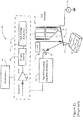
- a typical AFM system is shown schematically in Figure 11 .
- An AFM 10 employs a probe device 12 including a probe 17 having a cantilever 15.
- a scanner 24 generates relative motion between the probe 17 and a sample 22 while the probe-sample interaction is measured. In this way, images or other measurements of the sample can be obtained.
- Scanner 24 is typically comprised of one or more actuators that usually generate motion in three mutually orthogonal directions (XYZ).
- scanner 24 is a single integrated unit that includes one or more actuators to move either the sample or the probe in all three axes, for example, a piezoelectric tube actuator.
- the scanner may be a conceptual or physical combination of multiple separate actuators.
- Some AFMs separate the scanner into multiple components, for example an XY actuator that moves the sample and a separate Z-actuator that moves the probe.
- the instrument is thus capable of creating relative motion between the probe and the sample while measuring the topography or some other property of the sample as described, e.g., in Hansma et al. U.S. Pat. No. RE 34,489 ; Elings et al. U.S. Pat. No. 5,266,801 ; and Elings et al. U.S. Pat. No. 5,412,980 .
- probe 17 is often coupled to an oscillating actuator or drive 16 that is used to drive probe 17 to oscillate at or near a resonant frequency of cantilever 15.
- Alternative arrangements measure the deflection, torsion, or other characteristic of cantilever 15.
- Probe 17 is often a microfabricated cantilever with an integrated tip 17.
- an electronic signal is applied from an AC signal source 18 under control of an SPM controller 20 to cause actuator 16 (or alternatively scanner 24) to drive the probe 17 to oscillate.
- actuator 16 or alternatively scanner 24
- the probe-sample interaction is typically controlled via feedback by controller 20.
- the actuator 16 may be coupled to the scanner 24 and probe 17 but may be formed integrally with the cantilever 15 of probe 17 as part of a self-actuated cantilever/probe.
- a deflection detection apparatus 25 is typically employed to direct a beam towards the backside of probe 17, the beam then being reflected towards a detector 26, such as a four quadrant photodetector.
- the deflection detector is often an optical lever system such as described in Hansma et al. U.S. Pat. No. RE 34,489 , but may be some other deflection detector such as strain gauges, capacitance sensors, etc.
- the sensing light source of apparatus 25 is typically a laser, often a visible or infrared laser diode.
- controller 20 determines an error at Block 30, then generates control signals (e.g., using a PI gain control Block 32) to maintain a relatively constant interaction between the tip and sample (or deflection of the lever 15), typically to maintain a setpoint characteristic of the oscillation of probe 17.
- the control signals are typically amplified by a high voltage amplifier 34 prior to, for example, driving scanner 24.
- controller 20 is often used to maintain the oscillation amplitude at a setpoint value, A S , to insure a generally constant force between the tip and sample.
- a setpoint phase or frequency may be used.
- Controller 20 is also referred to generally as feedback where the control effort is to maintain a constant target value defined by the setpoint.
- a workstation 40 is also provided, in the controller 20 and/or in a separate controller or system of connected or stand-alone controllers, that receives the collected data from the controller 20 and manipulates the data obtained during scanning to perform data manipulation operating such as point selection, curve fitting, and distance determining operations.
- the workstation can store the resulting information in memory, use it for additional calculations, and/or display it on a suitable monitor.
- AFMs may be designed to operate in a variety of modes, including contact mode and oscillating mode. Operation is accomplished by moving the sample and/or the probe assembly up and down relatively perpendicular to the surface of the sample in response to a deflection of the cantilever of the probe assembly as it is scanned across the surface. Scanning typically occurs in an "x-y" plane that is at least generally parallel to the surface of the sample, and the vertical movement occurs in the "z" direction that is perpendicular to the x-y plane.
- TappingModeTM AFM is a trademark of the present assignee
- the tip is oscillated at or near a resonant frequency of the associated cantilever of the probe, or harmonic thereof.
- a feedback loop attempts to keep the amplitude of this oscillation constant to minimize the "tracking force," i.e., the force resulting from tip/sample interaction, typically by controlling tip-sample separation.
- Alternative feedback arrangements keep the phase or oscillation frequency constant. As in contact mode, these feedback signals are then collected, stored and used as data to characterize the sample.
- AFMs can obtain resolution down to the atomic level on a wide variety of insulating or conductive surfaces in air, liquid or vacuum by using piezoelectric scanners, optical lever deflection detectors, and very small cantilevers fabricated using photolithographic techniques. Because of their resolution and versatility, AFMs are important measurement devices in many diverse fields ranging from semiconductor manufacturing to biological research. Note that "SPM" and the acronyms for the specific types of SPMs, may be used herein to refer to either the microscope apparatus or the associated technique, e.g., "atomic force microscopy.”
- KPFM Kelvin-Probe Force Microscopy
- SPoM Surface Potential Microscopy
- SEPM Surface Electric Potential Microscopy
- SPMs scanning probe microscopes
- KPFM is a combination of atomic force microscopy (AFM) and Kelvin probe technique.
- Kelvin probe technique was designed to measure the contact potential difference (CPD) between an AFM probe and a sample surface when the two are brought close to one another.
- the CPD depends largely on the work function difference between the two materials.
- the work function of a sample under test can be deduced if the work function of the probe is calibrated against a sample having a well-defined work function.
- Traditional Kelvin probe technique has a high sensitivity for potential measurements but offers poor spatial resolution.
- the invention of atomic force microscope (AFM) by Binnig et al. in 1986 (U.S.
- Patent 4,724,318 opened the door to imaging solid sample surfaces of all kinds with nanometer to atomic resolution.
- Weaver et al. adapted Kelvin probe technique and combined it with AFM in 1991 (" High Resolution Atomic Force Microscopy Potentiometry ", Weaver et al., J. Vac. Sci. Technol. B Vol. 9, No. 3, May/Jun 1991, pp. 1559-1561 );
- Nonnenmacher et al. coined the term Kelvin probe force microscopy shortly after (“ Kelvin Probe Force Microscopy", Nonnenmacher et al., Appl. Phys. Lett. Vol. 58, No. 25, June 1991, pp. 2921-2923 ).
- Kelvin Probe Force Microscopy Nonnenmacher et al.
- Appl. Phys. Lett. Vol. 58, No. 25, June 1991, pp. 2921-2923 Thereafter, different AFM modes and KPFM detection schemes have appeared, and the various combinations of them have flourished the
- KPFM is based on force measurement, employing the sensitive force detection capability in an AFM.
- Frequency-modulation KPFM Frequency-modulation KPFM (FM-KPFM) was introduced in 1991 by Nonnenmacher et al, and was perfected under ultrahigh vacuum in 1998 by Kitamura et al. (" High-resolution Imaging of Contact Potential Difference with Ultrahigh Vacuum Noncontact Atomic Force Microscope", Kitamura et al., Appl. Phys. Lett. Vol. 72, No. 24, June 1998, pp. 3154-3156 ; and U.S. Patent 6,073,485 ).
- the cantilever is mechanically driven by a tapping piezo at or near the resonance frequency of the cantilever f , and an AC bias is applied between the probe and the sample with a frequency f m usually much lower than the fundamental probe resonant frequency.
- the AC bias modulates the electric force gradient between the probe and the sample, thus periodically changing the effective spring constant of the cantilever; this causes the resonance frequency to shift periodically, that is, to modulate, at f m and 2 f m .
- an FM-KPFM 100 includes a) an AFM control block 102 configured to operate the AFM in either intermittent contact mode (AM-AFM) or non-contact mode (FM-AFM), and b) a KPFM control block 104.
- AFM 102 includes a probe 106 having a lever 108 supporting a tip 110 that is caused to interact with a sample 112 (note the charge distribution shown on the sample indicating electrical properties to be measured).
- AM-AFM intermittent contact mode
- FM-AFM non-contact mode
- KPFM control block 104 includes a probe 106 having a lever 108 supporting a tip 110 that is caused to interact with a sample 112 (note the charge distribution shown on the sample indicating electrical properties to be measured).
- AM-AFM mode an AC voltage is applied to the tapping piezo 114 by source 113 to cause the AFM cantilever to oscillate at or near its resonance frequency f 1 .
- Deflection of probe 106 during operation is measured by directing a laser beam from source 115 toward the backside of lever 108 and toward detector 117.
- the deflection signal from detector 117 is transmitted to signal processing block 118 of AFM control block 102 to determine an appropriate control signal to maintain probe-sample interaction at a setpoint.
- This feedback control signal (together with a scanning control signal provided in block 120) is transmitted to an actuator 116 (e.g., an X-Y-Z piezoelectric tube) to appropriately position the probe supported thereby.
- FM-KPFM control block 104 includes a source 128 that provides an AC bias at frequency f 2 , usually a few kHz, applied between the probe and the sample, giving rise to an alternating electric force gradient between probe 106 and sample 112. This force gradient will cause the probe resonant frequency to modulate, manifested as sidebands at f 1 ⁇ n f 2 which are used for KPFM feedback.
- the sideband frequencies are known (Block 124) and input to lock-in amplifier 122 for comparison to the output signal of detector 117.
- a KPFM feedback block 126 operates to continuously adjust the DC bias (which is added to the AC bias at block 130) so that the probe response at the side bands ( f 1 ⁇ f 2 ) drops to 0. When doing so, the V dc equals the contact potential difference (CPD) between sample 112 and probe 106 providing one of the electrical properties of the sample at that location.
- CPD contact potential difference
- TappingMode requires use of probes having relatively high spring constants for reliable operation; and not too high a Q value to attain a bandwidth that allows a reasonably fast scan rate. KPFM sensitivity is thereby necessarily limited.
- Contact mode permits the use of levers having lower spring constants but is generally known to be one of the most destructive SPM techniques and is therefore limited with respect to which the types of samples with which it can be used.
- KPFM accuracy and resolution can also be limited by any one or more of the following: tip wear, tip contamination (need stable tip work function), metal degradation particularly over the apex, parasitic capacitance (compromise lateral resolution), parasitic electrochemistry, unintentional charge dissipation from the sample, etc.
- tip wear tip contamination (need stable tip work function)
- metal degradation particularly over the apex metal degradation particularly over the apex
- parasitic capacitance thus yield parasitic electrochemistry
- unintentional charge dissipation from the sample etc.
- KPFM is integrated with Tapping Mode (or intermittent contact mode or AC mode). Stability of the tapping mode critically depends on the spring constant of the cantilever probe k, where the common value of k is about 40 N/m and can be reduced to 5 N/m with marginal performance.
- the sensitivity factor of the KPFM detection is defined by Q / k , where Q is the mechanical quality factor of the cantilever. Given a typical "Q" of 200 on surface, normal KPFM usually have a sensitivity factor from 5-40. Using probes having a much lower spring constant is therefore desirable; however, low spring constant probes are incompatible with the requirements of Tapping Mode feedback stability.
- conventional AFM has been known for its inability to simultaneously acquire both high-resolution images and quantitative mechanical property information (e.g., elasticity, plasticity, and adhesion). Measuring mechanical properties with an AFM experimental setup is possible, but most known methods and systems rely on collecting force curves corresponding to the local tip-sample interaction, an extremely slow process.
- KPFM measurement systems are subject to large variations in the surface potential value, due primarily to changes at the probe apex during imaging.
- the surface potential of gold (Au) is around 800 mV.
- a first concern is drift during measurement. Drift can be substantial, often exceeding hundreds of mV, thereby making accurate measurements using AFM impractical.
- the measured surface potential varies when a probe is replaced or used for an extended period of time, and can also vary from system to system. These changes are typically caused by uncertainty and variation of the conductive coating on the AFM probe; in particular, the crystal structure of the apex of the tip is poorly defined and changes from probe to probe.
- an AFM probe 600 consists of two parts, a cantilever 602 which is sensitive to the forces between the tip and the sample, and a tip 604.
- the tip 604 includes a body 606 having a base 608 that connects to or is otherwise support by cantilever 602 and an apex 610 having a radius in nanometer range.
- Apex 610 is the part of the probe that interacts with the sample, with the resolution of the AFM substantially defined by the radii of the apex.
- KPFM measurement apparatus and methods utilize either i) a coated probe (conducting), where the conducting material at apex 610 is poorly defined due primarily to inherent imperfections in the coating process, or ii) an etched metal wire, the mechanical properties of which are poorly controlled during fabrication, as understood in the art. In either case, the KPFM measurement is compromised.
- the microscopy field has been left wanting a more comprehensive instrument capable of fast, high sensitivity electrical, topography, and mechanical sample property measurement.
- the tool would be capable of associating the measured electrical properties with the corresponding mechanical properties of the sample at each data acquisition location.
- the preferred embodiments are directed to high performance KPFM. More particularly, the invention is directed to an AFM that combines mechanical property measurement of a sample, e.g., on the nanoscale, with the capability to characterize electrical properties using a Kelvin probe configuration.
- the preferred embodiments make it possible to measure mechanical properties and electrical properties of a sample at the same time, with improved accuracy/resolution, at the nanometer scale, and associate that electrical property data with more credible topography and mechanical property information concerning the sample.
- the exemplary embodiments are able to achieve higher sensitivity factor as well as accuracy/repeatability improvements over known systems, primarily due to PFT mode's ability to support probes having higher sensitivity factor.
- the exemplary embodiments combine the mechanical and electrical capabilities of AFM to substantially fully characterize samples on, e.g., the nanometer scale. While PFT methods and apparatus operate to gather data concerning mechanical properties of a sample and KPFM methods and apparatus operate to gather data concerning electrical properties of a sample, the preferred embodiments make AFM more powerful by integrating the two together. Not only does the result improve user efficiency, but also allows in situ correlation of mechanical properties and electrical properties for very small features (i.e., high resolution), thus providing new information regarding a material's characteristics and performance.
- the probe of the exemplary embodiments has a tip including a body made of a homogeneous material (conducting) from its base to its apex.
- Homogeneous material means the same chemical composition, physical properties (including conductivity), crystalline orientation and surface potential.
- the tip is made of a homogeneous conducting material, with an insulating layer between the cantilever and tip base. The insulating layer can be optional but the homogeneous material of the tip (base to apex) must always be present.
- the tip and the cantilever are made of one homogeneous material that is conducting. Using either of these embodiments of the probe, the accuracy of the present KPFM measurement is substantially improved.
- a method for measuring multiple properties of a sample includes providing an atomic force microscope (AFM) including a probe having a cantilever and a tip. The method also includes operating the AFM to cause the probe to interact with the sample in a two pass procedure. During a first pass of the two pass procedure, a surface of the sample is detected by operating the AFM in PFT Mode. Then, during a second pass of the two pass procedure, electrical property data corresponding to the sample is collected.
- AFM atomic force microscope
- the method includes acquiring at least one of topography and mechanical property data during the detecting step.
- the acquiring step may include collecting mechanical property data and the mechanical property data includes at least one of elasticity, stiffness, plasticity, viscoelasticity and hardness.
- the probe has a sensitivity factor ( Q / k ) greater than 40.
- the second pass of the collecting step includes using at least one of FM-KPFM and AM-KPFM.
- a DC bias employed in the second pass is set to zero in the first pass, and an AC bias is preferably set to equal half the fundamental cantilever resonant frequency in the second pass.
- the probe in another aspect of the preferred embodiments, includes a cantilever and a tip, and the tip includes a body having a base and an apex, and wherein the body of the tip is made of a homogeneous material.
- an insulating layer may be disposed between the cantilever and the tip.
- a combination of the cantilever and the tip may be made of a single homogeneous material, with no insulating layer.
- a SPM configured in accordance with another preferred embodiment includes providing an atomic force microscope (AFM) having a probe defining a tip. The material of the entire tip is homogeneous.
- the method also includes providing relative scanning motion between the probe and a sample causing the probe to interact with the sample.
- the AFM is operated to collect topography data, mechanical property data and electrical property data with the probe in one of a group including a single pass procedure and a two pass procedure.
- the operating step includes using PFT mode to collect the topography data and the mechanical property data. More specifically, the operating step may be performed as a two pass procedure using LiftModeTM, and the topography data collected in a first pass of the two pass procedure is used in the second pass.
- the second pass includes using FM-KPFM and wherein the FM modulation step includes providing first and second lock-in amplifiers in a cascade configuration.
- the probe has a spring constant less than 1 N/m.
- a method of operating a SPM includes a second pass of a two pass procedure using a high voltage detection circuit to measure a surface potential of the sample greater than ⁇ 12 volts.
- the second pass includes applying an AC bias voltage between the probe and the sample.
- the AC bias voltage has a frequency lower than one-half the resonant frequency of the probe.
- the method includes performing a thermal tuning step to determine the fundamental resonant frequency of the probe.
- a method for measuring multiple properties of a sample includes providing an atomic force microscope (AFM) including a probe having a tip, and operating the AFM to cause the probe to interact with the sample in a one pass procedure.
- the method also includes collecting topographic and mechanical property data corresponding to the sample using PFT mode, and collecting electrical property data corresponding to the sample with the probe using KPFM.
- AFM atomic force microscope
- the probe has an insulating cantilever with a conductive tip made of a single material on one side, and a conductive coating on the other side made of a pure metal
- a method of operating an atomic force microscope (AFM) to measure a sample includes providing an AFM including a probe having a tip, wherein the entire tip is made of a homogeneous material.
- the AFM is opened in peak force tapping (PFT) mode, and the method includes collecting KPFM data during said operating step.
- PFT peak force tapping
- the method includes performing a thermal tuning step to determine the fundamental resonant frequency of the probe.
- PFT mode AFM The benefits of PFT mode AFM are numerous. Most noteworthy is its capability of simultaneous quantitative mechanical property mapping and topographical imaging. Moreover, its ability to use cantilevers having properties (spring constant, resonant frequency and quality factor) over a wide range allows for probe selection most suited to KPFM operation. It is the object of this invention to combine PFT mode AFM with KPFM, preferably FM-KPFM, and AM-KPFM as an alternative. This will offer simultaneous surface topography, mechanical properties, and surface potential (electrical property) mapping with enhanced sensitivity. Ease-of-use operation also benefits beginner users for getting high quality data without intensive learning and practicing. The implementation and benefits will be outlined below.
- Peak Force Tapping Mode provides a solution to the quantitative mechanical property mapping.
- the tip With the tip driven in and out of the contact with the surface at multi-kilohertz frequency, the tip's position and mechanical response (bending and thus reflection) are recorded. The recorded data resembles conventional force curve data and are thus analyzed based on a well-defined model. Mechanical properties, such as elasticity, plasticity, adhesion, etc., can be derived for the localized area under the probe's apex. It is notable that the process to capture data and do the analysis is done at very high speed (sub-milliseconds) and therefore quantitative mapping with high special resolution is achieved.
- AFM Peak Force Tapping (PFT) mode is described in U.S. Ser. No. 12/618,641 filed Nov. 13, 2009 , entitled Method and Apparatus of Operating a Scanning Probe Microscope and US Ser. No 13/306,867, filed November 29, 2011 , and entitled Method and Apparatus of Using Peak Force Tapping Mode to Measure Physical Properties of a Sample.
- PFT Mode the AFM drives the cantilever at a frequency far lower than the resonant frequency, contrary to TappingMode, allowing essentially instantaneous force monitoring and control.
- Sample imaging and mechanical property mapping are achieved with improved resolution and high sample throughput, with operation suitable in air, fluid and vacuum environments.
- PFT mode facilitates ease-of-use operation, where an algorithm may be employed to automatically adjust the AFM imaging feedback gain, force setpoint and scan rate based on a predetermined noise threshold.
- PFT mode provides substantial advantages regarding mechanical property characterization on the nanometer scale, it is unable to provide all data some users need. For instance, characterization of electrical properties of the sample may be desired, including associating one or more electrical properties with one or more corresponding mechanical property characteristics (along with topography) at each data collection point.
- Kelvin Probe Force Microscopy is an established method using AFM to measure some electrical properties such as work function, electrical potential, local charge, dielectric constant, and so on. It uses the same principle as the traditional Kelvin probe.
- the probe of the AFM serves as the reference electrode which forms a capacitor with the surface under test.
- Traditional feedback or LiftModeTM is used to keep the distance between the probe and the sample surface constant.
- An alternating current (AC) voltage is applied to the probe. When the potential between the probe and the sample surface are different, the applied AC voltage will cause the cantilever to vibrate. By detecting this vibration and providing an additional DC offset to minimize it, the potential of the sample surface can be accurately measured.
- traditional KPFM does not give information about a material's mechanical properties.
- KPFM techniques using periodic excitations can benefit from operating the AFM so that the response of interest occurs at or near a cantilever resonance.
- F and x are the amplitudes of the sinusoidal force on the cantilever and the resulting displacement, respectively.
- the cantilever's spring constant is k and Q is the quality factor of its assumed resonance.
- the frequency shift corresponds to a phase shift, which is commonly used in FM-KPFM detection.
- Q / k of the cantilever leads to a bigger phase change, and thus higher measurement sensitivity for FM-KPFM.
- FM-KPFM under vacuum enjoys high sensitivity thanks to the high Q (usually 2 ⁇ 3 orders of magnitude higher than in air).
- Q usually 2 ⁇ 3 orders of magnitude higher than in air.
- SPM operation in air which is one of the major advantages of SPM over other high-resolution microscopes such as SEM, potential Q values are limited.
- the lowest possible spring constant is important for sensitive KPFM in air.
- standard TappingMode SPM operation requires using probes having relatively high spring constants for reliable operation (e.g., the probe tip may stick to the surface of the sample), and not too high a Q value to attain a bandwidth that allows a reasonably fast scan rate. Therefore, KPFM sensitivity is necessarily limited.
- PFT mode AFM lifts the restrictions associated with intermittent-contact mode (TappingMode).
- probes having a wide range of characteristics can be used to enhance KPFM detection sensitivity.
- typical KPFM probes have a sensitivity factor Q / k of around 40.
- probes having a corresponding Q / k ratio above 40, as well as above 100 and even 200, can be employed with the present preferred embodiments.
- the probe tip is not homogeneous; rather, it may be, for example, a silicon tip with a metal coating to make the tip conductive. It has been discovered that performing KPFM using a probe having an inhomogeneous tip can severely limit the accuracy of the acquired KPFM data.
- the probe is made to be homogeneous. "Homogeneous" in the context of the present application means that the probe is made of a single material with the same crystalline structure throughout its volume.
- the tip which includes a body defining a base (the base being coupled to the cantilever, either directly, or indirectly with an intermediate insulating layer (described further immediately below)), and an apex (the distal end of the probe tip which interacts with the sample during PF-KPFM operation).
- Probe 400 includes a cantilever 402 made of, for example, a silicon nitride insulating lever 406 with a tip made of a single homogeneous material (doped silicon, or pure metal) 404 extending therefrom.
- a pure metal e.g., aluminum
- cantilever 402 made of, for example, a silicon nitride insulating lever 406 with a tip made of a single homogeneous material (doped silicon, or pure metal) 404 extending therefrom.
- a pure metal e.g., aluminum
- a pure metal can be deposited on the backside or top surface of lever 402 to form a capacitor with tip 404.
- probe 400 operates to minimize current flow between the tip and sample. As a result, the chance that an electrochemical reaction occurs at the sample surface is minimized, and thus stability is improved. Moreover, when using probe 400, shifts in measured potential due to tip wear are lessened given that the work function of the probe is dictated by the back side coating material. When employing probe 400, KPFM with 20 mV accuracy/repeatability, or better, can be achieved. This probe will also limit charge dissipation of the sample.
- probe 400 does not require insulating layer 406 (and thus is shown as optional in Figure 7 ).
- the entire probe 400 is made of a single homogeneous material.
- the entire probe could be made of a metal or it could be made of an appropriately doped silicon, with no insulating layer, with a metal (such as aluminum) deposited on its backside for optical detection of probe deflection.
- the tip remains homogeneous and thus the work function of the probe material remains constant and accurate KPFM data (e.g., to 50 mV) can be obtained.
- a capacitor 410 may be added in series to a regular conductive probe to achieve similar effect, though care must be taken with capacitor selection or compromised data (e.g., streaks) may result due to static charge hang-over in capacitor 410.
- a combination of peak force tapping technology and Kelvin probe measurement is shown as a KPFM instrument 150 including a control block 160 and a data collection unit 162.
- the integration of these two state-of-the-art techniques is realized through LiftModeTM operation, i.e., a two pass procedure.
- LiftModeTM operation i.e., a two pass procedure.
- single pass procedure and two (or dual) pass are used. These terms refer to the relative scanning motion between the probe and the sample (in XY) during AFM operation being performed either once or twice on the same scan line in a raster scan (e.g., LiftModeTM).
- KPFM 150 includes a probe 152 defining a cantilever 154 supporting a tip 156 at its distal end. Probe 152 is scanned across the surface of a sample 158 while the probe is oscillated generally at a multi-kilohertz off-resonance frequency. The deflection of the lever 154 is monitored and sent to a PFT mode control block 164 which operates to keep the tip sample force at the PFT setpoint. As understood, it is the control provided by PFT mode that may yield signals indicative of mechanical properties of the sample surface, as well as topography. This data is stored in data collection unit 162 depicted in Figure 1 as blocks 166 and 168, respectively.
- the tip preferably is lifted up some constant distance "Z" from the surface to follow the surface profile on a second pass/scan of sample surface 158 during which a Kelvin probe measurement is made using a KPFM algorithm 170.
- a simple lift at a user-selected distance may be employed in the second pass of the scan, i.e., topography data, though preferred, need not be collected and used in the second pass; rather, the lift and second pass may be performed regardless of whether the topography is known from the first pass.
- the electrical property, mechanical property and topography information can then be combined to render a composite view of different surface features of sample 158.
- Implementations of the KPFM including a PF-FM-KPFM ( Figure 2 ) and a PF-AM-KPFM ( Figure 3 ) are described below.
- a PF-FM-KPFM 180 includes PFT mode AFM hardware including a probe 182 defining a cantilever 184 supporting a tip 186.
- an AC bias is applied to an actuator 192 coupled to probe 182 to oscillate probe 182 at a multi-kilohertz frequency during a first pass (governed by control block 198; control block 206 is the KPFM control block).
- Tip 186 of PF-FM-KPFM 180 is thereby caused to interact with the surface of a sample 188.
- the deflection of probe 182 is monitored by directing a laser beam from a source 194 toward the backside of lever 184, which is then reflected to a detector 196, such as a quadrant photo detector 196.
- Detector 196 transmits this deflection signal to a peak force algorithm block 200.
- Peak force algorithm block 200 generates a signal indicative of the force corresponding to the detected deflection, and that force signal is compared to a force setpoint at block 202.
- a PFT mode controller 204 determines an appropriate control signal "S" based on the detected force which is transmitted to an actuator 192 (e.g., a piezoelectric XYZ tube) to appropriately position probe 182 in "Z.” At each X-Y location of the sample, the interaction is captured to generate a force curve from which several mechanical properties of the sample can be derived. Note that KPFM block 206 is not operational during the first pass in which the DC bias (between the probe and the sample is maintained (e.g., set) at zero.
- PFT mode can be performed automatically, in which at least one of the feedback gain, scan rate, and peak force setpoint can be set by the system software. Moreover, though preferred, mechanical property mapping need not be included. When it is, PF-KPFM provides simultaneous (with topography imaging) property mapping of at least one of adhesion, elasticity, hardness, plasticity, surface deformation and energy dissipation, for example.
- probe 182 is "lifted” a fixed distance "z" (usually a few nanometers, up to a few hundred nanometers) from the surface.
- An AC signal at frequency f 1 is applied to the tapping piezoelectric actuator 190 which oscillates the probe at or near its mechanical resonance frequency f 1 .
- a second AC bias signal at frequency f 2 is applied to the sample which produces an AC electric field between the probe and the sample.
- the overall effect is a probe response with side bands at f 1 ⁇ nf 2 frequencies.
- the KPFM feedback scheme continues to adjust the DC bias so that the side bands at f 1 ⁇ f 2 vanishes manifesting that the electric force gradient is nullified.
- the potential at the surface of sample 188 at that XY location is therefore quantified / measured, i.e., the applied DC voltage equals the CPD.
- a dual frequency AC bias can be used: with the first frequency at half the resonance frequency of the cantilever, which replaces the mechanical drive to cause the probe to vibrate at its resonant frequency; and the second frequency again at a few kilohertz.
- a PF-AM-KPFM 220 is employed as shown in Figure 3 .
- PF-AM-KPFM 220 includes PFT mode AFM hardware including a probe 222 defining a cantilever 224 supporting a tip 226.
- tip 226 interacts with a surface of a sample 228, the deflection is monitored, for example, by providing a laser source 234 which directs light toward the backside of cantilever 224 for reflection to a detector 236.
- the Z-position of probe 222 is controlled by PFT feedback to follow the sample surface.
- Probe 222 is made to oscillate in the "Z" direction to periodically touch the surface of sample 228.
- PFT feedback is implemented using PFT algorithm at block 240 which generates a force signal in response to the deflection signal, the force signal being compared to a force setpoint at block 242.
- a controller 244 determines an appropriate PFT control signal "S" to be applied to an actuator 232 (XYZ piezoelectric tube, for example) to adjust the Z-position of probe 222 coupled thereto to maintain the tip-sample force at the setpoint.
- KPFM block 246 is not operational during the first pass in which the DC bias (between the probe and the sample is maintained (e.g., set) at zero.
- the cantilever is lifted a fixed distance "z" from the sample 228.
- An AC bias signal at frequency f 1 from source 250 is applied between the probe and the sample at frequency f 1 .
- a KPFM feedback algorithm 248 determines a DC bias based on the detected deflection of probe 222, the DC bias being combined with the AC bias at block 252 to continuously adjust the DC bias so that the probe's oscillation at f 1 is minimized.
- f 1 is minimized, there is no DC electrical field between the probe and the sample.
- the potential at the sample surface at that XY location is therefore quantified / measured, i.e., the applied DC voltage equals the CPD.
- KPFM including both PF-FM-KPFM and PF-AM-KPFM can operate with feedback off thereby essentially reducing KPFM to an electric force microscope (EFM), where phase or amplitude will be measured instead of potential.
- EFM electric force microscope
- FIG. 4 the FM modulation/demodulation in the PF-FM-KPFM embodiment shown in Figure 2 is shown.
- Two lock-in amplifiers 278, 280 in cascade are used to implement the FM demodulation (block 208, Figure 2 ), and related feedback.
- AC signal 1 (f 1 ) is generated by source 276 and applied to a piezoelectric actuator 268 (tapping piezo) supporting a probe 262 defining a lever 264 having a tip 266 at its distal end. Deflection of the probe is monitored by an optical detection scheme including a laser 272 which directs a light beam at the backside of lever 264 so it is reflected toward a detector 274.
- An actuator 268 (e.g., a tapping piezoelectric actuator) oscillates probe 262 at the probe's resonant frequency.
- a second AC signal at frequency f 2 generated by a source 282 is applied to a sample 270. This causes the frequency at which probe 262 oscillates to vary, which is reflected in the phase change of the f 1 component and can be detected by Lock-in Amplifier (LIA) one 278.
- LIA Lock-in Amplifier
- the output of LIA 278 can be phase, amplitude, in-phase and quadrature, but preferably phase.
- the output of LIA 278 is then fed to Lock-in amplifier two 280 to determine its amplitude (A phase ) at the f 2 frequency, which is essentially the amplitude at sidebands f 1 ⁇ f 2 .
- This is used by the feedback algorithm of controller 284 to determine an appropriate DC bias to be applied to sample 270 (combined with AC Signal 2 at block 286) to nullify A phase .
- the potential of sample 270 is quantified / measured with reference to probe 262.
- two LIAs in cascade are shown and described, alternatives are contemplated. For instance, a combination of a filter and a lock-in amplifier could be used, as well as a combination of a frequency-voltage converter and a lock-in amplifier.
- a method 290 of operating the KPFM according to a preferred embodiment is shown in Figure 5 .
- the laser for the optical detection set-up is aligned with the probe and the method auto adjusts the PF-KPFM (FM or AM) operating parameters in Block 293.
- a fast thermal tune algorithm is also employed to determine the thermal peak frequency (fundamental resonant frequency of the probe) which is used as the AC bias drive frequency (f 1 ) by either a) drive 214 of PF-FM-KPFM of Figure 2 , or b) drive 250 of PF-AM-KPFM of Figure 3 .
- the fast thermal tune algorithm is described in US Prov. Pat. Appl.
- the preferred embodiments are capable of collecting absolute value KPFM electrical data with 20 mV accuracy.
- the KPFM apparatus and methods of the preferred embodiments are completely instrument and probe independent, facilitating significant improvements in operator ease of use.
- Method 290 then operates to engage surface at Block 294, for example, using a rapid engage algorithm such as that shown and described in US Pat. No. 7,665,349 .
- Relative scanning motion between the probe and sample is initiated and AFM is operated in PFT mode as part of a first pass in Block 298.
- the bias voltage is set to zero.
- the KPFM is operated as part of a second pass of relative motion between the sample and probe in Block 302.
- the bias voltage is applied. KPFM data can then be collected and stored according to the above described techniques in Block 304.
- Figure 6 illustrates a preferred embodiment in which a single pass is employed to collect topography, mechanical and electrical property data concerning the sample surface.
- a method 310 includes a start up and initialization step at block 312. Thereafter, the probe and sample are engaged with one another in block 314.
- both the KPFM algorithm and the PFT algorithm are operated substantially simultaneously to acquire topography, mechanical property and electrical property data in a single pass.
- the data acquired in block 316 is then collected and stored for each XY position in block 318.
- the method 290 illustrated in Figure 5 may in some cases be preferred to minimize adverse effects due to crosstalk.
- KPFM-HV 500 A high voltage KPFM instrument (KPFM-HV) 500 is shown in Figure 8 and described below.
- KPFM-HV 500 is preferably configured to operate as a two-pass method employing PFT mode AFM; however, as an alternative, AM-AFM or FM-AFM may be used.
- the first pass uses feedback control as part of an AFM configuration 501 to determine physical properties of the sample, including topography, while the second pass employs a high voltage detection circuit 502 to collect KPFM data.
- a probe 504 including a cantilever 505 supporting a tip 506 is caused to interact with a sample 508 by driving it in to oscillation using a tapping piezo 516 or other piezoelectric actuator.
- Deflection of probe 504 is detected by detector 512 and transmitted to a signal processing block 518 that outputs a force control signal (PFT mode) that together with the scan control signal from position control block 520 appropriately positions the probe relative to the sample via appropriate signals sent to XYZ actuator 514.
- PFT mode force control signal
- an AC bias at a frequency lower than half of the cantilever resonant frequency is applied between the probe and the sample via source 527. This AC bias causes the relative motion between the probe and sample to oscillate at a frequency f , as well as at its 2nd harmonic.
- the amplitude at these frequencies is determined using a pair of lock-in amplifiers, Lock-In Amplifier one 522 (AC bias frequency (FM) 1-20 kHz, phase: +90°) and Lock-In Amplifier two 524, respectively.
- the electric potential between the tip and sample can be calculated at Block 526 based on the oscillation amplitude at frequencies f and 2 f .
- potential Pontential sign Phase 1 * 1 4 V ac Af A 2 f
- v dc 0 and the voltage/potential data is stored at block 528.
- KPFM feedback is not employed in this high voltage detection regime.
- Figure 9 is directed to a method 530 associated with the high voltage KPFM-HV shown in Figure 8 , using a two-pass approach (LiftModeTM).
- method 530 engages the probe on the sample surface in Block 534.
- Relative scanning motion between the probe and the sample is provided in Block 536 (raster scan, e.g.) while PFT mode feedback is provided in Block 538.
- Block 536 raster scan, e.g.
- PFT mode feedback is provided in Block 538.
- surface topography and mechanical property data is collected.
- Block 540 the probe is lifted a certain amount "z" and a second pass is initiated.
- the amplitude response of the probe is determined at frequencies f and 2 f using lock-in amplifiers ( Figure 8 ).
- Method 530 then calculates potential in Block 542.
- the data is then compiled to generate a 3D topography map and a 2D mechanical property map from the PFT mode control signals, and a corresponding 2D potential map from the 2 nd pass data, in Block 544.
- Figure 10 is directed to a method 550 associated with the KPFM-HV shown in Figure 8 , using a single pass approach.
- method 550 provides relative scanning motion between the probe and the sample in Block 554.
- both PFT mode feedback and KPFM-HV detection circuitry are operated simultaneously in Blocks 558 and 562, respectively.
- the potential is calculated in Block 564 and the data is then compiled in Block 560 to generate a 3D topography map and a 2D mechanical property map from the PFT mode control signals, and a corresponding 2D potential map from the KPFM-HV detection branch.
- the preferred embodiments offer simultaneous acquisition of surface topography, mechanical properties, and surface potential (electrical property) mapping.
- PFT mode AFM's ability to use cantilevers having properties (spring constant, resonant frequency and quality factor) over a wide range can be used to the advantage of KPFM measurement. For instance, probes with low spring constant and high quality factors that are restricted for Tapping mode operation, now can be used to enhance KPFM detection sensitivity.
- the preferred embodiments also improve the KPFM measurement repeatability by extending the lifetime of the probes.
- the force exerted to the tip and sample can be much smaller in peak force tapping mode than in tapping mode or contact mode. Tip wear and tear is therefore greatly reduced, which benefits KPFM spatial resolution (tip remains sharp over long scan time) and measurement consistency.
- Ease-of-use is another advantage.
- Traditional KPFM uses TappingMode or contact mode to acquire the surface profile data.
- Tapping Mode is complicated by (a) indirect force control, (b) cantilever resonance dynamics of multiple harmonics, and (c) amplitude or phase of the probe oscillation during data acquisition can be affected by many factors other than the tip-sample interaction force. Due to these complications, subjective judgment must be employed, most often requiring much knowledge and experience. Even in contact mode AFM, constant drift of the cantilever deflection due to thermal or other system factors makes accurate force control generally impossible.
- PFT mode is used to acquire topographic data. PFT mode eliminates many of the complications discussed above. The criteria used to judge optimal imaging parameters become simple and objective. As a result, the measurement procedure can be automated.
- the resonant frequency of the probe may be readily determined using thermal tuning (automatically).
- the phase can be set automatically.
- the mechanical drive amplitude is preferably automatically set to drive probe oscillation at optimal amplitude to enhance operational consistency.
Landscapes
- Physics & Mathematics (AREA)
- Health & Medical Sciences (AREA)
- General Health & Medical Sciences (AREA)
- General Physics & Mathematics (AREA)
- Nuclear Medicine, Radiotherapy & Molecular Imaging (AREA)
- Radiology & Medical Imaging (AREA)
- Engineering & Computer Science (AREA)
- Power Engineering (AREA)
- Length Measuring Devices With Unspecified Measuring Means (AREA)
- Investigating Strength Of Materials By Application Of Mechanical Stress (AREA)
Applications Claiming Priority (3)
| Application Number | Priority Date | Filing Date | Title |
|---|---|---|---|
| US201261663528P | 2012-06-22 | 2012-06-22 | |
| PCT/US2013/047372 WO2013192617A1 (fr) | 2012-06-22 | 2013-06-24 | Méthode et appareil de mesure de propriété électrique utilisant un afm fonctionnant en mode contact intermittent à maximum de force |
| EP13806671.7A EP2864798B1 (fr) | 2012-06-22 | 2013-06-24 | Méthode et appareil de mesure de propriété électrique utilisant un afm fonctionnant en mode contact intermittent à maximum de force |
Related Parent Applications (2)
| Application Number | Title | Priority Date | Filing Date |
|---|---|---|---|
| EP13806671.7A Division EP2864798B1 (fr) | 2012-06-22 | 2013-06-24 | Méthode et appareil de mesure de propriété électrique utilisant un afm fonctionnant en mode contact intermittent à maximum de force |
| EP13806671.7A Division-Into EP2864798B1 (fr) | 2012-06-22 | 2013-06-24 | Méthode et appareil de mesure de propriété électrique utilisant un afm fonctionnant en mode contact intermittent à maximum de force |
Publications (2)
| Publication Number | Publication Date |
|---|---|
| EP3293527A2 true EP3293527A2 (fr) | 2018-03-14 |
| EP3293527A3 EP3293527A3 (fr) | 2018-08-29 |
Family
ID=52697083
Family Applications (2)
| Application Number | Title | Priority Date | Filing Date |
|---|---|---|---|
| EP13806671.7A Active EP2864798B1 (fr) | 2012-06-22 | 2013-06-24 | Méthode et appareil de mesure de propriété électrique utilisant un afm fonctionnant en mode contact intermittent à maximum de force |
| EP17197571.7A Pending EP3293527A3 (fr) | 2012-06-22 | 2013-06-24 | Mèthode et appareil de mesure de propriètè èlectrique utilisant un afm fonctionnant en mode contact intermittent à maximum de force |
Family Applications Before (1)
| Application Number | Title | Priority Date | Filing Date |
|---|---|---|---|
| EP13806671.7A Active EP2864798B1 (fr) | 2012-06-22 | 2013-06-24 | Méthode et appareil de mesure de propriété électrique utilisant un afm fonctionnant en mode contact intermittent à maximum de force |
Country Status (3)
| Country | Link |
|---|---|
| EP (2) | EP2864798B1 (fr) |
| KR (2) | KR101655051B1 (fr) |
| WO (1) | WO2013192617A1 (fr) |
Families Citing this family (11)
| Publication number | Priority date | Publication date | Assignee | Title |
|---|---|---|---|---|
| KR101630392B1 (ko) * | 2014-10-24 | 2016-06-15 | 파크시스템스 주식회사 | 토포그래피 신호 및 옵션 신호 획득 방법, 장치 및 이를 구비하는 원자 현미경 |
| KR102102637B1 (ko) * | 2016-04-28 | 2020-04-22 | 파크시스템스 주식회사 | 토포그래피 신호 및 옵션 신호 획득 방법, 장치 및 이를 구비하는 원자 현미경 |
| EP3285075A1 (fr) * | 2016-08-19 | 2018-02-21 | Consejo Superior De Investigaciones Cientificas | Dispositif et procédé de mappage d'échantillons piézoélectriques et/ou ferroélectriques |
| CN106645808B (zh) * | 2017-02-21 | 2019-07-02 | 哈尔滨工业大学 | 一种多参数同步测量的开尔文探针力显微镜 |
| EP3432007B1 (fr) * | 2017-07-18 | 2020-02-26 | IMEC vzw | Dispositif et procédé de profilage bidimensionnel de porteur active de composants à semi-conducteurs |
| KR102186234B1 (ko) | 2020-04-23 | 2020-12-03 | 정동진 | 카드 소독기 |
| CN111965391B (zh) * | 2020-08-17 | 2023-07-14 | 中国科学院宁波材料技术与工程研究所 | 一种表征纳米材料稳定性的方法 |
| CN112666369A (zh) * | 2020-12-24 | 2021-04-16 | 广州中源仪器技术有限公司 | 原子力显微镜系统 |
| CN113092826B (zh) * | 2021-03-05 | 2023-04-07 | 中山大学 | 扫描探针显微镜系统及其测量方法 |
| WO2022258084A1 (fr) | 2021-07-13 | 2022-12-15 | Ceske Vysoke Uceni Technicke V Praze | Procédé d'examen d'un échantillon dans un microscope à force atomique |
| AT525244B1 (de) * | 2021-10-12 | 2023-02-15 | Univ Wien Tech | Verfahren zum betrieb eines rasterkraftmikroskops und regel- und steuereinheit hierfür |
Citations (6)
| Publication number | Priority date | Publication date | Assignee | Title |
|---|---|---|---|---|
| US4724318A (en) | 1985-11-26 | 1988-02-09 | International Business Machines Corporation | Atomic force microscope and method for imaging surfaces with atomic resolution |
| US5266801A (en) | 1989-06-05 | 1993-11-30 | Digital Instruments, Inc. | Jumping probe microscope |
| USRE34489E (en) | 1989-03-13 | 1993-12-28 | The Regents Of The University Of California | Atomic force microscope with optional replaceable fluid cell |
| US5412980A (en) | 1992-08-07 | 1995-05-09 | Digital Instruments, Inc. | Tapping atomic force microscope |
| US6073485A (en) | 1997-07-11 | 2000-06-13 | Jeol Ltd. | Scanning microscope for image topography and surface potential |
| US7665349B2 (en) | 2005-04-12 | 2010-02-23 | Veeco Instruments Inc. | Method and apparatus for rapid automatic engagement of a probe |
Family Cites Families (10)
| Publication number | Priority date | Publication date | Assignee | Title |
|---|---|---|---|---|
| US5267471A (en) * | 1992-04-30 | 1993-12-07 | Ibm Corporation | Double cantilever sensor for atomic force microscope |
| JPH07120482A (ja) * | 1993-10-25 | 1995-05-12 | Nikon Corp | 原子間力と電気容量とを同時に検出するための原子間力顕微鏡用プローブおよびその製造方法 |
| JPH08201400A (ja) * | 1995-01-30 | 1996-08-09 | Nikon Corp | 表面形状ならびに局所的静電容量同時計測用 カンチレバー |
| JPH08320325A (ja) * | 1995-03-20 | 1996-12-03 | Ricoh Co Ltd | 物理量測定装置 |
| JP3925991B2 (ja) * | 1997-07-08 | 2007-06-06 | 日本電子株式会社 | 走査プローブ顕微鏡 |
| US7473887B2 (en) * | 2002-07-04 | 2009-01-06 | University Of Bristol Of Senate House | Resonant scanning probe microscope |
| US6975129B2 (en) * | 2003-06-17 | 2005-12-13 | National Applied Research Labratories | Electrical scanning probe microscope apparatus |
| US7415868B2 (en) * | 2005-03-21 | 2008-08-26 | Multiprobe, Inc. | Deconvolving tip artifacts using multiple scanning probes |
| US8650660B2 (en) * | 2008-11-13 | 2014-02-11 | Bruker Nano, Inc. | Method and apparatus of using peak force tapping mode to measure physical properties of a sample |
| US8342867B2 (en) | 2009-12-01 | 2013-01-01 | Raytheon Company | Free floating connector engagement and retention system and method for establishing a temporary electrical connection |
-
2013
- 2013-06-24 KR KR1020157001820A patent/KR101655051B1/ko not_active Application Discontinuation
- 2013-06-24 WO PCT/US2013/047372 patent/WO2013192617A1/fr unknown
- 2013-06-24 EP EP13806671.7A patent/EP2864798B1/fr active Active
- 2013-06-24 EP EP17197571.7A patent/EP3293527A3/fr active Pending
- 2013-06-24 KR KR1020167023920A patent/KR101991556B1/ko active IP Right Grant
Patent Citations (7)
| Publication number | Priority date | Publication date | Assignee | Title |
|---|---|---|---|---|
| US4724318A (en) | 1985-11-26 | 1988-02-09 | International Business Machines Corporation | Atomic force microscope and method for imaging surfaces with atomic resolution |
| USRE34489E (en) | 1989-03-13 | 1993-12-28 | The Regents Of The University Of California | Atomic force microscope with optional replaceable fluid cell |
| USRE34489F1 (en) | 1989-03-13 | 1999-12-14 | Univ California | Atomic force microscope with optimal replacement fluid cell |
| US5266801A (en) | 1989-06-05 | 1993-11-30 | Digital Instruments, Inc. | Jumping probe microscope |
| US5412980A (en) | 1992-08-07 | 1995-05-09 | Digital Instruments, Inc. | Tapping atomic force microscope |
| US6073485A (en) | 1997-07-11 | 2000-06-13 | Jeol Ltd. | Scanning microscope for image topography and surface potential |
| US7665349B2 (en) | 2005-04-12 | 2010-02-23 | Veeco Instruments Inc. | Method and apparatus for rapid automatic engagement of a probe |
Non-Patent Citations (3)
| Title |
|---|
| KITAMURA ET AL.: "High-resolution Imaging of Contact Potential Difference with Ultrahigh Vacuum Noncontact Atomic Force Microscope", APPL. PHYS. LETT., vol. 72, no. 24, June 1998 (1998-06-01), pages 3154 - 3156, XP012020431, DOI: doi:10.1063/1.121577 |
| NONNENMACHER ET AL.: "Kelvin Probe Force Microscopy", APPL. PHYS. LETT., vol. 58, no. 25, June 1991 (1991-06-01), pages 2921 - 2923, XP000232731, DOI: doi:10.1063/1.105227 |
| WEAVER ET AL.: "High Resolution Atomic Force Microscopy Potentiometry", J. VAC. SCI. TECHNOL. B, vol. 9, no. 3, pages 1559 - 1561, XP000222582, DOI: doi:10.1116/1.585423 |
Also Published As
| Publication number | Publication date |
|---|---|
| KR101655051B1 (ko) | 2016-09-06 |
| WO2013192617A1 (fr) | 2013-12-27 |
| EP2864798A1 (fr) | 2015-04-29 |
| KR101991556B1 (ko) | 2019-06-20 |
| KR20150033673A (ko) | 2015-04-01 |
| EP2864798B1 (fr) | 2021-11-03 |
| EP3293527A3 (fr) | 2018-08-29 |
| KR20160106204A (ko) | 2016-09-09 |
| EP2864798A4 (fr) | 2016-03-30 |
Similar Documents
| Publication | Publication Date | Title |
|---|---|---|
| US9869694B2 (en) | Method and apparatus of electrical property measurement using an AFM operating in peak force tapping mode | |
| EP2864798B1 (fr) | Méthode et appareil de mesure de propriété électrique utilisant un afm fonctionnant en mode contact intermittent à maximum de force | |
| US7155964B2 (en) | Method and apparatus for measuring electrical properties in torsional resonance mode | |
| US9995765B2 (en) | Method and apparatus of using peak force tapping mode to measure physical properties of a sample | |
| US8646109B2 (en) | Method and apparatus of operating a scanning probe microscope | |
| US9274139B2 (en) | Method and apparatus of operating a scanning probe microscope | |
| US6945099B1 (en) | Torsional resonance mode probe-based instrument and method | |
| KR101298782B1 (ko) | 비틀림 공진 모드에서 전기적 성질을 측정하기 위한 방법 및 장치 | |
| US8869311B2 (en) | Displacement detection mechanism and scanning probe microscope using the same |
Legal Events
| Date | Code | Title | Description |
|---|---|---|---|
| PUAI | Public reference made under article 153(3) epc to a published international application that has entered the european phase |
Free format text: ORIGINAL CODE: 0009012 |
|
| STAA | Information on the status of an ep patent application or granted ep patent |
Free format text: STATUS: REQUEST FOR EXAMINATION WAS MADE |
|
| 17P | Request for examination filed |
Effective date: 20171020 |
|
| AC | Divisional application: reference to earlier application |
Ref document number: 2864798 Country of ref document: EP Kind code of ref document: P |
|
| AK | Designated contracting states |
Kind code of ref document: A2 Designated state(s): AL AT BE BG CH CY CZ DE DK EE ES FI FR GB GR HR HU IE IS IT LI LT LU LV MC MK MT NL NO PL PT RO RS SE SI SK SM TR |
|
| RIN1 | Information on inventor provided before grant (corrected) |
Inventor name: MITTEL, HENRY Inventor name: SU, CHANMIN Inventor name: HE, JIANLI Inventor name: WANG, WEIJE Inventor name: HU, YAN Inventor name: MINNE, STEPHEN, C. Inventor name: LI, CHUNZENG Inventor name: HU, SHUIQING Inventor name: MA, JI Inventor name: HUANG, LIN |
|
| PUAL | Search report despatched |
Free format text: ORIGINAL CODE: 0009013 |
|
| AK | Designated contracting states |
Kind code of ref document: A3 Designated state(s): AL AT BE BG CH CY CZ DE DK EE ES FI FR GB GR HR HU IE IS IT LI LT LU LV MC MK MT NL NO PL PT RO RS SE SI SK SM TR |
|
| RIC1 | Information provided on ipc code assigned before grant |
Ipc: G01Q 60/30 20100101AFI20180720BHEP Ipc: G01Q 60/40 20100101ALI20180720BHEP Ipc: G01Q 60/34 20100101ALI20180720BHEP |
|
| STAA | Information on the status of an ep patent application or granted ep patent |
Free format text: STATUS: EXAMINATION IS IN PROGRESS |
|
| 17Q | First examination report despatched |
Effective date: 20210423 |
|
| STAA | Information on the status of an ep patent application or granted ep patent |
Free format text: STATUS: EXAMINATION IS IN PROGRESS |