EP3290784A1 - Lichtemittierendes modul und anzeigevorrichtung mit dem lichtemittierenden modul - Google Patents
Lichtemittierendes modul und anzeigevorrichtung mit dem lichtemittierenden modul Download PDFInfo
- Publication number
- EP3290784A1 EP3290784A1 EP17188664.1A EP17188664A EP3290784A1 EP 3290784 A1 EP3290784 A1 EP 3290784A1 EP 17188664 A EP17188664 A EP 17188664A EP 3290784 A1 EP3290784 A1 EP 3290784A1
- Authority
- EP
- European Patent Office
- Prior art keywords
- light
- face
- light source
- distance
- emitting module
- Prior art date
- Legal status (The legal status is an assumption and is not a legal conclusion. Google has not performed a legal analysis and makes no representation as to the accuracy of the status listed.)
- Pending
Links
Images







Classifications
-
- G—PHYSICS
- G02—OPTICS
- G02B—OPTICAL ELEMENTS, SYSTEMS OR APPARATUS
- G02B6/00—Light guides; Structural details of arrangements comprising light guides and other optical elements, e.g. couplings
- G02B6/0001—Light guides; Structural details of arrangements comprising light guides and other optical elements, e.g. couplings specially adapted for lighting devices or systems
- G02B6/0011—Light guides; Structural details of arrangements comprising light guides and other optical elements, e.g. couplings specially adapted for lighting devices or systems the light guides being planar or of plate-like form
- G02B6/0033—Means for improving the coupling-out of light from the light guide
- G02B6/0063—Means for improving the coupling-out of light from the light guide for extracting light out both the major surfaces of the light guide
-
- G—PHYSICS
- G02—OPTICS
- G02B—OPTICAL ELEMENTS, SYSTEMS OR APPARATUS
- G02B6/00—Light guides; Structural details of arrangements comprising light guides and other optical elements, e.g. couplings
- G02B6/0001—Light guides; Structural details of arrangements comprising light guides and other optical elements, e.g. couplings specially adapted for lighting devices or systems
- G02B6/0011—Light guides; Structural details of arrangements comprising light guides and other optical elements, e.g. couplings specially adapted for lighting devices or systems the light guides being planar or of plate-like form
- G02B6/0066—Light guides; Structural details of arrangements comprising light guides and other optical elements, e.g. couplings specially adapted for lighting devices or systems the light guides being planar or of plate-like form characterised by the light source being coupled to the light guide
- G02B6/0068—Arrangements of plural sources, e.g. multi-colour light sources
-
- G—PHYSICS
- G02—OPTICS
- G02F—OPTICAL DEVICES OR ARRANGEMENTS FOR THE CONTROL OF LIGHT BY MODIFICATION OF THE OPTICAL PROPERTIES OF THE MEDIA OF THE ELEMENTS INVOLVED THEREIN; NON-LINEAR OPTICS; FREQUENCY-CHANGING OF LIGHT; OPTICAL LOGIC ELEMENTS; OPTICAL ANALOGUE/DIGITAL CONVERTERS
- G02F1/00—Devices or arrangements for the control of the intensity, colour, phase, polarisation or direction of light arriving from an independent light source, e.g. switching, gating or modulating; Non-linear optics
- G02F1/01—Devices or arrangements for the control of the intensity, colour, phase, polarisation or direction of light arriving from an independent light source, e.g. switching, gating or modulating; Non-linear optics for the control of the intensity, phase, polarisation or colour
- G02F1/13—Devices or arrangements for the control of the intensity, colour, phase, polarisation or direction of light arriving from an independent light source, e.g. switching, gating or modulating; Non-linear optics for the control of the intensity, phase, polarisation or colour based on liquid crystals, e.g. single liquid crystal display cells
- G02F1/133—Constructional arrangements; Operation of liquid crystal cells; Circuit arrangements
- G02F1/1333—Constructional arrangements; Manufacturing methods
- G02F1/1335—Structural association of cells with optical devices, e.g. polarisers or reflectors
- G02F1/1336—Illuminating devices
- G02F1/133615—Edge-illuminating devices, i.e. illuminating from the side
-
- G—PHYSICS
- G02—OPTICS
- G02B—OPTICAL ELEMENTS, SYSTEMS OR APPARATUS
- G02B6/00—Light guides; Structural details of arrangements comprising light guides and other optical elements, e.g. couplings
- G02B6/0001—Light guides; Structural details of arrangements comprising light guides and other optical elements, e.g. couplings specially adapted for lighting devices or systems
- G02B6/0011—Light guides; Structural details of arrangements comprising light guides and other optical elements, e.g. couplings specially adapted for lighting devices or systems the light guides being planar or of plate-like form
- G02B6/0013—Means for improving the coupling-in of light from the light source into the light guide
- G02B6/0015—Means for improving the coupling-in of light from the light source into the light guide provided on the surface of the light guide or in the bulk of it
- G02B6/002—Means for improving the coupling-in of light from the light source into the light guide provided on the surface of the light guide or in the bulk of it by shaping at least a portion of the light guide, e.g. with collimating, focussing or diverging surfaces
-
- G—PHYSICS
- G02—OPTICS
- G02B—OPTICAL ELEMENTS, SYSTEMS OR APPARATUS
- G02B6/00—Light guides; Structural details of arrangements comprising light guides and other optical elements, e.g. couplings
- G02B6/0001—Light guides; Structural details of arrangements comprising light guides and other optical elements, e.g. couplings specially adapted for lighting devices or systems
- G02B6/0011—Light guides; Structural details of arrangements comprising light guides and other optical elements, e.g. couplings specially adapted for lighting devices or systems the light guides being planar or of plate-like form
- G02B6/0066—Light guides; Structural details of arrangements comprising light guides and other optical elements, e.g. couplings specially adapted for lighting devices or systems the light guides being planar or of plate-like form characterised by the light source being coupled to the light guide
- G02B6/0073—Light emitting diode [LED]
-
- G—PHYSICS
- G02—OPTICS
- G02B—OPTICAL ELEMENTS, SYSTEMS OR APPARATUS
- G02B6/00—Light guides; Structural details of arrangements comprising light guides and other optical elements, e.g. couplings
- G02B6/0001—Light guides; Structural details of arrangements comprising light guides and other optical elements, e.g. couplings specially adapted for lighting devices or systems
- G02B6/0011—Light guides; Structural details of arrangements comprising light guides and other optical elements, e.g. couplings specially adapted for lighting devices or systems the light guides being planar or of plate-like form
- G02B6/0081—Mechanical or electrical aspects of the light guide and light source in the lighting device peculiar to the adaptation to planar light guides, e.g. concerning packaging
- G02B6/0086—Positioning aspects
- G02B6/0091—Positioning aspects of the light source relative to the light guide
-
- G—PHYSICS
- G02—OPTICS
- G02B—OPTICAL ELEMENTS, SYSTEMS OR APPARATUS
- G02B6/00—Light guides; Structural details of arrangements comprising light guides and other optical elements, e.g. couplings
- G02B6/0001—Light guides; Structural details of arrangements comprising light guides and other optical elements, e.g. couplings specially adapted for lighting devices or systems
- G02B6/0011—Light guides; Structural details of arrangements comprising light guides and other optical elements, e.g. couplings specially adapted for lighting devices or systems the light guides being planar or of plate-like form
- G02B6/0081—Mechanical or electrical aspects of the light guide and light source in the lighting device peculiar to the adaptation to planar light guides, e.g. concerning packaging
- G02B6/0095—Light guides as housings, housing portions, shelves, doors, tiles, windows, or the like
-
- G—PHYSICS
- G02—OPTICS
- G02F—OPTICAL DEVICES OR ARRANGEMENTS FOR THE CONTROL OF LIGHT BY MODIFICATION OF THE OPTICAL PROPERTIES OF THE MEDIA OF THE ELEMENTS INVOLVED THEREIN; NON-LINEAR OPTICS; FREQUENCY-CHANGING OF LIGHT; OPTICAL LOGIC ELEMENTS; OPTICAL ANALOGUE/DIGITAL CONVERTERS
- G02F1/00—Devices or arrangements for the control of the intensity, colour, phase, polarisation or direction of light arriving from an independent light source, e.g. switching, gating or modulating; Non-linear optics
- G02F1/01—Devices or arrangements for the control of the intensity, colour, phase, polarisation or direction of light arriving from an independent light source, e.g. switching, gating or modulating; Non-linear optics for the control of the intensity, phase, polarisation or colour
- G02F1/13—Devices or arrangements for the control of the intensity, colour, phase, polarisation or direction of light arriving from an independent light source, e.g. switching, gating or modulating; Non-linear optics for the control of the intensity, phase, polarisation or colour based on liquid crystals, e.g. single liquid crystal display cells
- G02F1/133—Constructional arrangements; Operation of liquid crystal cells; Circuit arrangements
- G02F1/1333—Constructional arrangements; Manufacturing methods
- G02F1/13338—Input devices, e.g. touch panels
-
- G—PHYSICS
- G06—COMPUTING OR CALCULATING; COUNTING
- G06F—ELECTRIC DIGITAL DATA PROCESSING
- G06F3/00—Input arrangements for transferring data to be processed into a form capable of being handled by the computer; Output arrangements for transferring data from processing unit to output unit, e.g. interface arrangements
- G06F3/01—Input arrangements or combined input and output arrangements for interaction between user and computer
- G06F3/03—Arrangements for converting the position or the displacement of a member into a coded form
- G06F3/041—Digitisers, e.g. for touch screens or touch pads, characterised by the transducing means
- G06F3/042—Digitisers, e.g. for touch screens or touch pads, characterised by the transducing means by opto-electronic means
- G06F3/0428—Digitisers, e.g. for touch screens or touch pads, characterised by the transducing means by opto-electronic means by sensing at the edges of the touch surface the interruption of optical paths, e.g. an illumination plane, parallel to the touch surface which may be virtual
-
- G—PHYSICS
- G02—OPTICS
- G02B—OPTICAL ELEMENTS, SYSTEMS OR APPARATUS
- G02B6/00—Light guides; Structural details of arrangements comprising light guides and other optical elements, e.g. couplings
- G02B6/0001—Light guides; Structural details of arrangements comprising light guides and other optical elements, e.g. couplings specially adapted for lighting devices or systems
- G02B6/0011—Light guides; Structural details of arrangements comprising light guides and other optical elements, e.g. couplings specially adapted for lighting devices or systems the light guides being planar or of plate-like form
- G02B6/0033—Means for improving the coupling-out of light from the light guide
- G02B6/0035—Means for improving the coupling-out of light from the light guide provided on the surface of the light guide or in the bulk of it
- G02B6/0045—Means for improving the coupling-out of light from the light guide provided on the surface of the light guide or in the bulk of it by shaping at least a portion of the light guide
- G02B6/0046—Tapered light guide, e.g. wedge-shaped light guide
-
- G—PHYSICS
- G02—OPTICS
- G02B—OPTICAL ELEMENTS, SYSTEMS OR APPARATUS
- G02B6/00—Light guides; Structural details of arrangements comprising light guides and other optical elements, e.g. couplings
- G02B6/0001—Light guides; Structural details of arrangements comprising light guides and other optical elements, e.g. couplings specially adapted for lighting devices or systems
- G02B6/0011—Light guides; Structural details of arrangements comprising light guides and other optical elements, e.g. couplings specially adapted for lighting devices or systems the light guides being planar or of plate-like form
- G02B6/0075—Arrangements of multiple light guides
- G02B6/0076—Stacked arrangements of multiple light guides of the same or different cross-sectional area
-
- G—PHYSICS
- G02—OPTICS
- G02B—OPTICAL ELEMENTS, SYSTEMS OR APPARATUS
- G02B6/00—Light guides; Structural details of arrangements comprising light guides and other optical elements, e.g. couplings
- G02B6/0001—Light guides; Structural details of arrangements comprising light guides and other optical elements, e.g. couplings specially adapted for lighting devices or systems
- G02B6/0011—Light guides; Structural details of arrangements comprising light guides and other optical elements, e.g. couplings specially adapted for lighting devices or systems the light guides being planar or of plate-like form
- G02B6/0081—Mechanical or electrical aspects of the light guide and light source in the lighting device peculiar to the adaptation to planar light guides, e.g. concerning packaging
- G02B6/0086—Positioning aspects
- G02B6/009—Positioning aspects of the light source in the package
Definitions
- the technical field relates to a light emitting module and a display device including a light emitting module.
- a display device may include a display panel for displaying an image according to received data.
- a liquid crystal display may include a liquid crystal panel for displaying an image by controlling an arrangement of liquid crystal molecules to adjust transmittance of light according to received data.
- the display panel e.g., the liquid crystal panel, itself may be of a non-emissive type. Therefore, the display device, e.g., the liquid crystal display, may include a light emitting module, e.g., a backlight unit, for providing light to the display panel.
- the backlight unit may include one or more of a light guide, a light source unit, a bottom chassis, a reflective sheet disposed in the bottom chassis to reflect light transmitted from the light guide toward the display panel, and a casing in which the light source unit is mounted.
- a dark region may be formed in the light guide depending on a position at which the light source is disposed.
- Embodiments may be related to a light emitting module and a display device having advantages of uniform light luminance distribution.
- An embodiment may be related to a light emitting module comprising a light guide, which includes a light-emitting surface, an opposite surface, a first face, a second face, and a third face, wherein the opposite surface is opposite the light-emitting surface, wherein each of the first face, the second face, and the third face is connected between the light-emitting surface and the opposite surface and is smaller than each of the light-emitting surface and the opposite surface, and wherein the second face is oriented angular or perpendicular to the first face and is connected through the third face to the first face; at least a first light source which faces the first face and is positioned with a center of a light-emitting surface thereof at a first distance from the third face; at least a second light source which faces the third face and is positioned with a center of a light-emitting surface thereof at a second distance from the first face, and wherein the second distance is greater than the first distance.
- coplanar refers to the orientation of two faces or surfaces relative to each other which are in a cross-sectional view parallel to each other.
- the light emitting module may comprise a plurality of first light sources and a plurality of second light sources, wherein a distance between the centers of the light-emitting surfaces of two of the second light sources is greater than a distance between the centers of the light-emitting surfaces of two of the first light sources.
- the third face may be oriented angular to the first face and the second face or may be rounded with a tangent that forms an obtuse angle with respect to the first face.
- the third face may include at least a first sub-face and at least a second sub-face connected angular or perpendicular to each other.
- the first sub-face may be oriented coplanar (parallel) to the first face.
- At least a second light source is positioned on the first sub-face and at least a second light source is positioned on the second sub-face.
- a distance between the center of the light-emitting surface of the second light source on the first sub-face and the center of the light-emitting surface of the second light source on the second sub-face is greater than a distance between the centers of the light-emitting surfaces of two of the first light sources.
- the second sub-face may be oriented at an obtuse angle or perpendicular with respect to at least one of the first face and the first sub-face.
- the second sub-face may be oriented coplanar (parallel) to the second face.
- the light emitting module may further comprise a substrate on or in which the at least first light source and the at least one second light source are mounted, wherein the substrate includes:
- the third substrate surface may be planar or curved.
- the light-emitting surface of the at least one first light source and the light-emitting surface of the at least one second light source are perpendicular to a mounting surface of the substrate in which the at least one first light source and the at least one second light source are mounted.
- the light-emitting surface of the at least one first light source and the light-emitting surface of the at least one second light source are coplanar (parallel) to a mounting surface of the substrate in which the at least one first light source and the at least one second light source are mounted.
- the light guide includes a pair of first faces facing away from each other and oriented coplanar to each other.
- the one of the first faces is shorter than the other of the first faces in a direction perpendicular to the light-emitting surface.
- An embodiment may be related to a light emitting module that includes the following elements: a light guide including a pair of light-emitting surfaces overlapping each other, a first surface formed in parallel (or coplanar) with a first direction to connect the light-emitting surfaces, a second surface formed in parallel with a second direction that is different from the first direction to connect the light-emitting surfaces, a third surface formed to connect the first surface with the second surface, and a boundary formed at a portion of the light guide at which the first surface and the third surface are connected with each other; and a light source unit configured to include a first light source disposed at the first surface, a second light source disposed at the third surface, and a substrate in which the first light source and the second light source are mounted, wherein a distance from a center of a light-emitting surface of the second light source to the boundary is greater than a distance from a center of a light-emitting surface of the first light source to the boundary.
- first light source there may be provided a plurality of first light sources
- second light source there may be provided a plurality of second light sources
- a distance between a center of one of the second light sources that is disposed nearest to the boundary and the boundary may be greater than a distance between a center of one of the first light sources that is disposed nearest to the boundary and the boundary.
- a distance between the second light sources may be greater than a distance between the first light sources.
- the third surface may include a plurality of faces.
- the third surface may include a first face set parallel to the first direction, and at least one second light source may be positioned on the first face.
- the first face set may include a plurality of first faces, and at least one second light source may be disposed on each of the first faces.
- the third surface may further include a second face set parallel to the second direction, and at least one second light source may be positioned on the first face.
- the second face set may include a plurality of second faces, and at least one second light source may be disposed on each of the second faces.
- the third surface may include a first face and a second face, the first face may be parallel to the first direction and a third direction that is different from the second direction, and the second face may be parallel to the first direction, the second direction, and a fourth direction that is different from the third direction.
- the third surface may include at least one curved surface.
- the substrate may include: a first substrate surface parallel to the first direction; a second substrate surface parallel to the second direction; and a third substrate surface configured to connect the first substrate surface with the second substrate surface.
- the third substrate surface may be planar or curved.
- the light-emitting surface of the first light source and the light-emitting surface of the second light source may be perpendicular to a mounting surface of the substrate in which the first light source and the second light source are mounted.
- the light-emitting surface of the first light source and the light-emitting surface of the second light source may be parallel to a mounting surface of the substrate in which the first light source and the second light source are mounted.
- the first surface may include a pair of first surfaces formed to face each other in the first direction.
- a width of a first one of the pair of first surfaces according to the first direction and a direction perpendicular to the second direction may be thicker than that of a second one of the pair of first surfaces according to the first direction and a direction perpendicular to the second direction.
- the pair of first surfaces may be symmetrical to each other.
- An embodiment may be related to a display device that includes the following elements: a display panel; and a light emitting module disposed in a first surface of the display panel, wherein the light emitting module includes: a light guide including a pair of light-emitting surfaces overlapping each other, a first surface formed in parallel with a first direction to connect the light-emitting surfaces, a second surface formed in parallel with a second direction that is different from the first direction to connect the light-emitting surfaces, a third surface formed to connect the first surface with the second surface, and a boundary formed at a portion of the light guide at which the first surface and the third surface are connected with each other; and a light source unit configured to include a first light source disposed at the first surface, a second light source disposed at the third surface, and a substrate in which the first light source and the second light source are mounted, wherein a distance from a center of a light-emitting surface of the second light source to the boundary is greater than a distance from a center of a light
- the display device may further include a touch portion disposed on a second surface of the display panel which faces the first surface, to include a plurality of infrared sensors, wherein the touch portion may include a first area formed to correspond to the first surface, a second area formed to correspond to the third surface, and a boundary area which serves as a boundary between the first area and the second area, and wherein a distance from a center of an infrared light-emitting surface of a second infrared sensor disposed in the second area to the boundary area may be greater than a distance from a center of an infrared light-emitting surface of a first infrared sensor disposed in the first area to the boundary area.
- the first infrared sensor may include a plurality of first infrared sensors and the second infrared sensor includes a plurality of second infrared sensors, and a distance between a center of an infrared light-emitting surface of one of the second infrared sensors that may be nearest to the boundary area and the boundary area is greater than a distance between a center of an infrared light-emitting surface of one of the first infrared sensors that is nearest to the boundary area and the boundary area.
- An embodiment may be related to a light emitting module.
- the light emitting module may include a light guide, a first light source set, and a second light source set.
- the light guide may include a light-emitting surface, an opposite surface, a first face, a second face, and a third face.
- the opposite surface may be opposite the light-emitting surface.
- Each of the first face, the second face, and the third face may be connected between the light-emitting surface and the opposite surface, may abut each of the light-emitting surface and the opposite surface, may be oriented not parallel to each of the light-emitting surface and the opposite surface, and may be smaller than each of the light-emitting surface and the opposite surface.
- the second face may be oriented not parallel to the first face and may be connected through the third face to the first face.
- the first light source set may face (and may directly contact) the first face for emitting first light toward the first face and may include a first first-set light source. No light source may be positioned between the first first-set light source and an edge of the first face.
- the second light source set may face (and may directly contact) the third face for emitting second light toward the third face and may include a first second-set light source. No light source may be positioned between the first second-set light source and an edge of the third face.
- a distance from a center of a light-emitting face of the first second-set light source to the edge of the third face may be greater than a distance from a center of a light-emitting face of the first first-set light source to the edge of the first face.
- a tangent to the third face may be oriented at an obtuse angle or a right angle with respect to the first face.
- the third face may be oriented at an obtuse angle with respect to the first face.
- the third face may be oriented at a right angle with respect to the first face.
- the third face may be oriented parallel to the first face.
- the third face may be a curved face.
- the edge of the first face coincides with the edge of the third face.
- the first light source set may include a second first-set light source. No light source may be positioned between the first first-set light source and the second first-set light source.
- the second light source set may include a second second-set light source. No light source may be positioned between the first second-set light source and the second second-set light source. A distance between (a center of) the first second-set light source and (a center of) the second second-set light source may be greater than a distance between (a center of) the first first-set light source and (a center of) the second first-set light source.
- the light guide may include a fourth face.
- Each of the second face and the third face may be connected through the fourth face to the first face.
- the third face may be oriented parallel to the first face.
- the light emitting module may include a third light source set, which may face the fourth face for emitting third light toward the fourth face and may include a first third-set light source.
- the first light source set may include a second first-set light source. No light source may be positioned between the first first-set light source and the second first-set light source. A distance between the first third-set light source and the first second-set light source in a direction parallel to the first face may be greater than a distance between the first first-set light source and the second first-set light source in the direction parallel to the first face.
- the fourth face may be oriented at an obtuse angle with respect to at least one of the first face and the third face.
- the fourth face may be oriented parallel to the second face.
- the light emitting module may include a substrate, which may include a curved substrate section that supports the second light source set.
- a total quantity of light sources of the first light source set may be greater than a total quantity of light sources of the second light source set.
- the first face may be longer than the third face.
- the light guide may include a fourth face, which may face the first face, may be oriented parallel to the first face, and may be shorter than the first face in a direction perpendicular to the light-emitting surface.
- the opposite surface may be oriented at an acute angle with respect to the light-emitting surface.
- the light guide may include a fourth face, which may be connected between the first face and the second face and may be connected between the light-emitting surface and the opposite surface. No light source may directly contact the fourth face.
- An embodiment may be related to a display device.
- the display device may include a display panel, a light guide, a first light source set, and a second light source set.
- the light guide may overlap the display panel and may include a first face, a second face oriented not parallel to the first face, a third face shorter than the first face and connected between the first face and the second face, and a light-emitting surface larger than each of the first face, the second face, and the third face.
- the first light source set may be disposed at the first face.
- the second light source may be disposed at the third face. A distance between two closest light sources of the second light source set may be greater than a distance between two closest light sources of the first light source.
- the display device may include a touch portion, a first infrared sensor set, and a second infrared sensor set.
- the touch portion may include a first area corresponding to the first surface and may include a second area corresponding to the third surface.
- the first infrared sensor set may be disposed at the first area and may include a first first-set infrared sensor. No infrared sensor may be positioned between the first first-set infrared sensor and an edge of the first area.
- the second infrared sensor set may be disposed at the second area and may include a first second-set infrared sensor. No infrared sensor may be positioned between the first second-set infrared sensor and an edge of the second area.
- a distance from a center of an infrared light-emitting surface of the first second-set infrared sensor to the edge of the second area may be greater than a distance from a center of an infrared light-emitting surface of the first first-set infrared sensor to the edge of the first area.
- a distance between two closet infrared sensors of the second infrared sensor set may be greater than a distance between two closest infrared sensors of the first infrared sensor set.
- a light emitting module and a display device may have substantially uniform light luminance distribution.
- first”, “second”, etc. may be used herein to describe various elements, these elements, should not be limited by these terms. These terms may be used to distinguish one element from another element. Thus, a first element discussed below may be termed a second element without departing from teachings of one or more embodiments. The description of an element as a “first” element may not require or imply the presence of a second element or other elements.
- the terms “first”, “second”, etc. may also be used herein to differentiate different categories or sets of elements. For conciseness, the terms “first”, “second”, etc. may represent “first-category (or first-set)", “second-category (or second-set)", etc., respectively.
- first element when referred to as being "on" a second element, the first element can be directly on the second element, or one or more intervening elements may also be present.
- FIG. 1 is a top plan view schematically illustrating a display device 1000
- FIG. 2 is an exploded perspective view schematically illustrating the display device 1000 according to an embodiment.
- the display device 1000 illustrated in FIG. 2 includes a light emitting module 100 including a light source unit 120 in which a light-emitting surface of first light sources 121 (see FIG. 3 ) and a light-emitting surface of second light sources 123 are substantially perpendicular to a mounting surface 125d of a substrate 125 on which the first light sources 121 and the second light sources 123 are mounted.
- the light emitting module 100 includes a display area DA and a peripheral area PA, and is used for the display device 1000 having a quadrangular shape with rounded corners.
- the light emitting module 100 is disposed in a surface of a display panel 200 to supply light to the display panel 200, and includes a light guide 110 and the light source unit 120.
- the display panel 200 serves to display a screen by using light supplied from the light emitting module 100.
- the light guide 110 serves to substantially uniformly supply light to the display panel 200 by diffusing the light supplied from the light source unit 120 by total reflection, and has a plate-like shape including a pair of light-emitting surfaces 111 or including a light-emitting surface 111 and an opposite surface opposite the light-emitting surface 111.
- the light-emitting surfaces 111 (or the light-emitting surface 111 and the opposite surface) are connected with each other by/through side faces 113, 115, and 117 including a face 113, a face 115, and a face 117.
- the face 113 is parallel to a first direction, and the face 115 is parallel to a second direction that is different from the first direction, especially perpendicular to the first direction.
- the first direction indicates an x-axis and the second direction indicates a y-axis.
- the face 113 may indicate a side surface formed at a long side of the light guide 110, and the face 115 may indicate a side surface at a short side of the light guide 110.
- the light emitting module 100 is used for the display device 1000 having the quadrangular shape with the rounded corners, and the light guide 110 included in the light emitting module 100 includes the face 117 formed at a position corresponding to one or more of the rounded corners of the display device 1000.
- the face 117 may have various shapes in various directions, and various examples of the face 117 will be described.
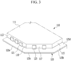
- FIG. 3 is an enlarged view illustrating a portion of a light emitting module 100 corresponding to an area A of the display device illustrated in FIG. 2
- FIG. 4 is a top plan view illustrating the light emitting module 100 of FIG. 3 .
- the light guide 110 includes the face 117 which connects the face 113 to the face 115.
- the face 117 is parallel to a third direction that is different from the first direction and the second direction, especially with a same angle to the first and second directions.
- the light guide 110 includes a boundary 119 (which may coincide with an edge of the face 113 and/or an edge of the face 117) formed at a position at which the face 113 is connected with the face 117.
- the face 113 and the face 117 may be divided from each other by the boundary 119, and the boundary 119 may be defined as an edge formed where the face 113 and the face 117 are connected with each other, or may be defined as a point where a direction changes while it is extended from the face 113 parallel to the first direction toward the face 117.
- the light source unit 120 includes the plurality of first light sources 121, the plurality of second light sources 123, and the substrate 125 (see FIG. 2 ).
- the first light sources 121 are disposed on the face 113 of the light guide 110 to supply light to the face 113
- the second light sources 123 are disposed on the face 117 of the light guide 110 to supply light to the face 117.
- the first light sources 121 and the second light sources 123 may be formed of light emitting diodes (LEDs).
- the substrate 125 includes the mounting surface 125d on which the first light sources 121 and the second light sources 123 are mounted, and a circuit (not illustrated) for driving the first light sources 121 and the second light sources 123.
- the substrate 125 similar to the light guide 110, includes a first substrate surface 125a parallel to the first direction, a second substrate surface 125b parallel to the second direction, and a third substrate surface 125c which connects the first substrate surface 125a with the second substrate surface 125b.
- the third substrate surface 125c may have a planar or curved shape to correspond to the shape of the face 117 of the light guide 110, but the shape of the third substrate surface 125c may not correspond to the shape of the face 117. This will be described later in detail when numerous modifications of the light guide 110 are described.
- a distance a2 from a center of a light-emitting surface of a second light source 123 disposed in the face 117 to the boundary 119 between the face 113 and the face 117 (or the edge of the face 113) is greater than a distance a1 from a center of a light-emitting surface of a first light source 121 disposed in the face 113 to the boundary 119 between the face 113 and the face 117 (or the edge of the face 117).
- the distance a2 to the center of the light-emitting surface of the second light source 123 disposed in the face 117 is greater than the distance a1 to the center of the light-emitting surface of the first light source 121 disposed in the face 113.
- the distance a2 may also be defined as distance between the center of a light-emitting surface of a second light source 123 disposed on the face 117 and the face 113, as the face 113 terminates at the boundary 119.
- the distance a1 may also be defined as distance between the center of a light-emitting surface of a first light source 121 disposed on the face 113 and the face 117, as the face 117 also terminates at the boundary 119.
- FIG. 5 and FIG. 6 are views for describing a difference depending on a variation of the distances from the boundary 119 to the first light sources 121 and second light sources 123 disposed in the face 113 and the face 117.
- FIG. 5 illustrates a first case that a distance a1' from the boundary 119 to the center of the light-emitting surface of the first light sources 121 is equal to a distance a2' from the boundary 119 to the center of the light-emitting surface of the second light sources 123
- FIG. 5 illustrates a first case that a distance a1' from the boundary 119 to the center of the light-emitting surface of the first light sources 121 is equal to a distance a2' from the boundary 119 to the center of the light-emitting surface of the second light sources 123
- FIG. 5 illustrates a first case that a distance a1' from the boundary 119 to the center of the light-emitting surface of the first light sources 121 is equal to a distance
- FIG. 6 illustrates a second case that the distance a2 from the boundary 119 to the center of the light-emitting surface of the second light sources 123 is greater than the distance a1 from the boundary 119 to the center of the light-emitting surface of the first light sources 121 as in the embodiment of FIG. 3 and FIG. 4 .
- the distance (a1', a1) between one of the first light sources 121 that is disposed nearest to the boundary 119 and the boundary 119 and the distance (a2', a2) between one of the second light sources 123 that is disposed nearest to the boundary 119 and the boundary 119 are measured for comparison.
- reference points of the first light sources 121 and the second light sources 123 are the centers of the light-emitting surfaces thereof.
- the distance a1' from the center of the light-emitting surface of the first light sources 121 to the boundary 119 is equal to the distance a2' from the center of the light-emitting surface of the second light sources 123 to the boundary 119.
- the distance a2 from the center of the light-emitting surface of the second light sources 123 to the boundary 119 is greater than the distance a1 from the center of the light-emitting surface of the first light sources 121 to the boundary 119.
- a distance b2 between the second light sources 123 may be greater than a distance b1 between the first light sources 121.
- the distance b1 between the first light sources 121 indicates a distance between centers of light-emitting surfaces of two first light sources 121 disposed (e.g., closest) adjacent to each other.
- the distance b2 between the second light sources 123 indicates a distance between centers of light-emitting surfaces of two second light sources 123 disposed (e.g., closet) adjacent to each other.
- This may be applied to a case that the distance b1 between the first light sources 121 and the distance b2 between the second light sources 123 are constant, but may also be applied to a case that the distance b1 between the first light sources 121 and the distance b2 between the second light sources 123 are not constant.
- a maximum or minimum of the distance b2 between the second light sources 123 may be greater than that of the distance b1 between the first light sources 121.
- the light guide 110 includes a face 117 including a plurality of faces 118, 118a, which also may be called face sections or sub-faces 118, 118a. In the following the sub-faces are called faces.
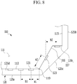
- FIG. 7 is an enlarged view illustrating a corner portion of the light emitting module 100 including the light guide 110 according to a first modification of the light guide 110 illustrated in FIG. 3
- FIG. 8 is a top plan view of the light emitting module 100 illustrated in FIG. 7 .
- the face 117 of the light guide 110 includes a face 118a parallel to the first direction.
- at least one second light source 123 may be disposed in the face 118a.
- one second light source 123 may be disposed in/on the face 118a, and one second light source 123 may be disposed in/on a face 118 of the face 117.
- a plurality of second light sources 123 may be disposed in/on the face 118a and/or a face 118 of the face 117, or only one second light source 123 may be disposed in/on the face 118a.
- the distance a2 from the center of the light-emitting surface of the second light sources 123 to the boundary 119 is greater than the distance a1 from the center of the light-emitting surface of the first light sources 121 to the boundary 119. Accordingly, similar to the light guide 110 illustrated in FIG 3 , an overlapped amount of light emitted from the first light sources 121 and the second light sources 123 may be reduced. Thus, it is easy to adjust light luminance.
- the distance b2 between the second light sources 123 may be greater than the distance b1 between the first light sources 121.
- the distance b1 between the first light sources 121 indicates a distance between (e.g., closest) two first light sources 121 disposed adjacent to each other, according to the first direction.
- the distance b2 between the second light sources 123 indicates a distance between (e.g. closest) two second light sources 123 disposed adjacent to each other, according to the first direction.
- FIG. 9 is an enlarged view illustrating a corner portion of the light emitting module 100 including the light guide 110 according to a second modification of the light guide 110 illustrated in FIG. 3
- FIG. 10 is a top plan view of the light emitting module 100 illustrated in FIG. 9 .
- the face 117 of the light guide 110 includes a plurality of faces 118a parallel to the face 113 and/or parallel to the first direction.
- at least one second light source 123 may be disposed in/on each of the faces 118a.
- FIG. 9 and FIG. 10 illustrate an example in which one second light source 123 is disposed in/on each of the faces 118a.
- the face 117 may further include a face 118b parallel to the second direction. At least one second light source 123 may be disposed in/on the face 118b.
- FIG. 9 and FIG. 10 illustrate an example in which the face 117 includes a plurality of faces 118b. Referring to FIG. 9 and FIG. 10 , in an embodiment, at least one second light source 123 may be disposed in each of the faces 118b.
- the distance a2 from the center of the light-emitting surface of a second light source 123 to the boundary 119 (or an edge of the face 118b) is greater than the distance a1 from the center of the light-emitting surface of the first light sources 121 to the boundary 119 (or an edge of the face 113). Accordingly, similar to the light guide 110 illustrated in FIG 3 , an overlapped amount of light emitted from the first light sources 121 and the second light sources 123 may be reduced. Thus, it is easy to adjust light luminance.
- the distance b2 between (e.g., two closest of) the second light sources 123 may be greater than the distance b1 between (e.g., two closest of) the first light sources 121.
- the distance b1 between the first light sources 121 indicates a distance between (e.g., closest) two first light sources 121 disposed adjacent to each other.
- the distance b2 between the second light sources 123 indicates a distance between (e.g., closest) two second light sources 123 disposed adjacent to each other.
- FIG. 11 is an enlarged view illustrating a corner portion of the light emitting module 100 including the light guide 110 according to a third modification of the light guide 110 illustrated in FIG. 3
- FIG. 12 is a top plan view of the light emitting module 100 illustrated in FIG. 11 .
- the face 117 of the light guide 110 includes a face 118a and a face 118b.
- each of the face 118a and the face 118b is disposed in parallel to a direction that is different from the first direction and the second direction.
- each of the face 118a which may be again called sub-face 118a
- the face 118b which might be called sub-face 118b
- the face 118a is disposed in parallel to a third direction that is different from the first direction and the second direction
- the face 118b is disposed in parallel to a fourth direction that is different from the first direction, the second direction, and the third direction.
- FIG. 11 and FIG. 12 illustrate an example in which the second light source 123 is disposed only in/on the face 118a.
- at least one second light source 123 may be disposed in/on the face 118a and/or the face 118b.
- the distance a2 from the center of the light-emitting surface of an edge second light source 123 to the boundary 119 is greater than the distance a1 from the center of the light-emitting surface of an edge first light source 121 to the boundary 119. Accordingly, similar to the light guide 110 illustrated in FIG 3 , an overlapped amount of light emitted from the first light sources 121 and the second light sources 123 may be reduced. Thus, it is easy to adjust light luminance.
- the distance b2 between the second light sources 123 may be greater than the distance b1 between the first light sources 121.
- the distance b1 between the first light sources 121 indicates a distance between (e.g., closest) two first light sources 121 disposed adjacent to each other.
- the distance b2 between the second light sources 123 indicates a distance between (e.g., closest) two second light sources 123 disposed adjacent to each other.
- the face 117 of the light guide 110 may include a plurality of faces or surfaces.
- the substrate 125 (see FIG. 2 ) of the light source unit 120 may include only one third substrate surface 125c which connects the first substrate surface 125a to the second substrate surface 125b.
- the third substrate surface 125c may include a plurality of faces which correspond to the faces of the face 117 of the light guide 110.
- FIG. 13 is an enlarged view illustrating a corner portion of the light emitting module 100 including the light guide 110 according to a fourth modification of the light guide 110 illustrated in FIG. 3
- FIG. 14 is a top plan view of the light emitting module 100 illustrated in FIG. 13 .
- the light guide 110 includes a face 117 formed as one curved surface.
- the second light sources 123 disposed in the face 117 may be disposed along the curved face 117.
- a tangent to the curved face 117 in a center portion thereof may be oriented at an obtuse angle with respect to the face 113.
- the substrate 125 (see FIG. 125) of the light source module includes a third substrate surface 125c which connects the first substrate surface 125a to the second substrate surface 125b and has at least one curved surface corresponding to the shape of the face 117 of the light guide 110.
- the third substrate surface 125c of the substrate 125 may include substantially flat faces regardless of the curved structure of the face 117 of the light guide 110.
- the distance a2 from the center of the light-emitting surface of an edge second light source 123 to the boundary 119 is greater than the distance a1 from the center of the light-emitting surface of an edge first light source 121 to the boundary 119 (which may coincide with an end of the face 113 at which the curvature of the face 117 begins). Accordingly, similar to the light guide 110 illustrated in FIG 3 , an overlapped amount of light emitted from the first light sources 121 and the second light sources 123 may be reduced. Thus, it is easy to adjust light luminance.
- the distance b2 between the second light sources 123 may be greater than the distance b1 between the first light sources 121.
- the distance b1 between the first light sources 121 indicates a distance between (e.g., closest) two first light sources 121 disposed adjacent to each other in the first direction.
- the distance b2 between the second light sources 123 indicates a distance between (e.g., closest) two second light sources 123 disposed adjacent to each other in the first direction.
- FIG. 13 and FIG. 14 illustrate an example in which the face 117 of the light guide 110 connects the face 113 to the face 115 and includes only one curved face.
- the face 117 may include a plurality of curved faces having different curvature radii or curvatures.
- the light emitting module 100 includes the light source unit 120 in which the light-emitting surfaces of the first light sources 121 and the second light sources 123 are perpendicular to the mounting surface 125d of the substrate 125 onto which the first light sources 121 and the second light sources 123 are mounted. This is referred to as a side-view type of light source unit 120.
- FIG. 15 and FIG. 16 illustrate the light emitting module 100 including the light source unit 120 in which the light-emitting surfaces of the first light sources 121 and the second light sources 123 are parallel to the mounting surface of the substrate 125 in which or onto which the first light sources 121 and the second light sources 123 are mounted according to an embodiment.
- This is referred to as a top-view type of light source unit 120.
- FIG. 16 is an enlarged view illustrating a portion of the light emitting module 100 corresponding to an area B of the display device 1000 illustrated in FIG. 15
- FIG. 17 is a top plan view illustrating the light emitting module 100 of FIG. 16 .
- FIG. 16 and FIG. 17 illustrate the light guide 110 including the face 117 which connects the face 113 to the face 115.
- the distance a2 from the center of the light-emitting surface of an edge second light source 123 to the boundary 119 is greater than the distance a1 from the center of the light-emitting surface of an edge first light source 121 to the boundary 119 (which may coincide an edge of the face 113), analogous to the embodiment of FIG. 3 and the first modification to the fourth modification of FIG. 3 .
- the distance a2 from the center of the light-emitting surface of the second light source 123 to the boundary 119 is greater than the distance a1 from the center of the light-emitting surface of the first light source 121 to the boundary 119. Accordingly, similar to the light guide 110 illustrated in FIG 3 , an overlapped amount of light emitted from the first light sources 121 and the second light sources 123 may be reduced. Thus, it is easy to adjust light luminance.
- the distance b2 between the second light sources 123 may be greater than the distance b1 between the first light sources 121.
- the distance b1 between the first light sources 121 indicates a distance between (e.g., closest) two first light sources 121 disposed adjacent to each other.
- the distance b2 between the second light sources 123 indicates a distance between (e.g., closest) two second light sources 123 disposed adjacent to each other.
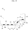
- FIG. 18 is an enlarged view illustrating a corner portion of the light emitting module 100 including the light guide 110 according to a first modification of FIG. 16
- FIG. 19 is a top plan view illustrating the light emitting module 100 illustrated in FIG. 18 .
- the light guide 110 illustrated in FIG. 18 and FIG. 19 according to the first modification of FIG. 16 includes a face 117 formed of a plurality of faces 118 and 118a, similar to the aforementioned light guide 110 illustrated in FIG. 7 .
- a face 118a may be oriented parallel to the face 113 and/or parallel to the first direction, and a face 118 may be oriented at an obtuse angle or a right angle with respect to the face 113.
- the distance a2 from the center of the light-emitting surface of an edge second light source 123 to the boundary 119 is greater than the distance a1 from the center of the light-emitting surface of an edge first light source 121 to the boundary 119. Therefore, similar to the aforementioned embodiment and the aforementioned modification, it is easier to adjust light luminance.
- the distance b2 between the second light sources 123 may be greater than the distance b1 between the first light sources 121.
- the distance b1 between the first light sources 121 indicates a distance between two first light sources 121 disposed adjacent/closest to each other.
- the distance b2 between the second light sources 123 indicates a distance between two second light sources 123 disposed adjacent/closest to each other.
- the light guide 110 may include a pair of faces 113 disposed in parallel.
- the pair of faces 113 may face away from each other.
- a width of a first one of the pair of faces 113 may be greater than that of a second one of the pair of faces 113 in a direction perpendicular to the light-emitting surface 111 of the light guide 110.
- FIG. 20 illustrates that light guides 110, including first light guides I and second light guides II, are alternately stacked.
- a width h1 of a first one of the pair of faces 113 is larger than a width h2 of a second one of the pair of faces 113.
- a light guide II may be equivalent to a reoriented/flipped light guide I.
- the face 113 having the larger width h1 in the first light guide I is stacked on (and may be coplanar with) the face 113 having the smaller width h2 in the second light guide II, and the ace 113 having the smaller width h2 in first light guide I is stacked on (and may be coplanar with) the face 113 having the larger width h1 in the second light guide II.
- the width h1 of one surface is larger than the width h2 of the other surface. If surfaces having the same widths are stacked on a same side, the stack may be inclined, such that manufacturing and/or storage of the light guides I and II may be difficult. Therefore, it is advantageous to form a stable stacked structure by alternately stacking aces of the light guides 110 (including light guides I and light guides II) having different thicknesses at a same side.
- light guides I and light guides II are alternately stacked. Accordingly, referring to FIG. 20 and FIG. 21 , it is possible to obtain a combined light guide stack that includes the first light guides I and the second light guides II and has a pair of opposite faces having substantially equal widths.
- FIG. 1 is a top plan view illustrating the display device 1000 according to an embodiment
- FIG. 2 is an exploded perspective view schematically illustrating the display device 1000 according to an embodiment
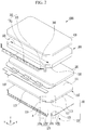
- FIG. 15 is an exploded perspective view illustrating constituent elements of the display device 1000 according to an embodiment.
- the display device 1000 may include the display panel 200 and the light emitting module 100 Referring to FIG. 2 and FIG. 15 .
- the display panel 200 which serves to display a screen by using light supplied from the light emitting module 100 may have rounded corners for the application to the display device 1000 with the rounded corners Referring to FIG. 1 .
- the light emitting module 100 includes a light guide 110 and a light source unit 120.
- FIG. 2 and FIG. 15 illustrate modifications depending on a disposal relationship between light sources of the light source units 120 and the substrate 125. Specifically, FIG. 2 illustrates the side-view type of light source unit 120, and FIG. 15 illustrates the top-view type of light source unit 120.
- the display device 1000 may include the light emitting module 100 corresponding to numerous modifications of the aforementioned light guides in addition to the modifications illustrated in FIG. 2 and FIG. 15 . Descriptions related to these modifications are the same as described above, and thus a redundant description will be omitted.
- the display device 1000 further includes a touch portion 300.
- the touch portion 300 may control the display device 1000 by sensing touches and/or receiving signals.
- the touch portion 300 includes an infrared sensor set for determining a distance from a sensing target and/or a magnitude of an input signal by irradiating infrared rays to the sensing target and measuring a speed/time of return of the infrared rays.
- the infrared sensor set may include a plurality of infrared sensors 310.
- the touch portion 300 is also for application to the display device 1000 with the rounded corners.
- the touch portion 300 includes a first area 320 which corresponds to the face 113 of the light guide 110, a second area 330 which corresponds the face 117 of the light guide 110, and a boundary 340 which corresponds to the boundary 119 of the light guide 110 as a boundary between the first area 320 and the second area 330 and may coincide with an edge of the area 320 and/or an edge of the area 330.
- FIG. 22 is an enlarged view schematically illustrating a corner of the touch portion 300 according to an embodiment, which corresponds an area B of FIG. 2 and FIG. 15
- FIG. 23 is a top plan view illustrating the touch portion 300 illustrated in FIG. 22 .
- one of the infrared sensors 310 which is disposed in/or (and disposed closed to the edge of) the first area 320 is defined as a first infrared sensor 311
- one of the infrared sensors 310 which is disposed in/or (and disposed closed to the edge of) the second area 330 is defined as a second infrared sensor 313.
- a distance c2 from a center of an infrared light-emitting surface of the second infrared sensor 313 to the boundary 340 is greater than a distance c1 from a center of an infrared light-emitting surface of the first infrared sensor 311 to the boundary 340.
- first infrared sensor 311 there may be provided a plurality of first infrared sensors 311 and instead of a single second infrared sensor 313 there may be provided a plurality of second infrared sensors 313.
- first infrared sensors 311 and the second infrared sensors 313 the distance c2 between a center of an infrared light-emitting surface of one of the second infrared sensors 313 which is nearest to the boundary 340 and the boundary 340 is compared with the distance c1 between a center of an infrared light-emitting surface of one of the first infrared sensors 311 which is nearest to the boundary area and the boundary 340.
- the distance c2 between a center of an infrared light-emitting surface of one of the second infrared sensors 313 which is nearest to the boundary 340 and the boundary 340 is greater than the distance c1 between a center of an infrared light-emitting surface of one of the first infrared sensors 311 which is nearest to the boundary 340 and the boundary 340.
- the distance c1 between a center of an infrared light-emitting surface of one of the first infrared sensors 311 which is nearest to the boundary 340 and the boundary 340 may be compared with a distance c2 between a center of an infrared light-emitting surface of the second infrared sensor 313 and the boundary 340.
- modifications of the first light sources 121 and the second light sources 123 of the light emitting module 100 described above may be similarly applied to the first infrared sensors 311 and the second infrared sensors 313.
- the display device 1000 may further include a window or transparent plate 400 disposed to protect against external impact and contamination on the display panel 200 and the touch portion 300.
- the window 400 may be formed of generally-used transparent glass or resin, and may be formed to have rounded corners to be applied to the display device 1000 having the rounded corners according to an embodiment.
- a light emitting module and/or a display device may have substantially uniform light luminance distribution.
Landscapes
- Physics & Mathematics (AREA)
- General Physics & Mathematics (AREA)
- Optics & Photonics (AREA)
- Engineering & Computer Science (AREA)
- Nonlinear Science (AREA)
- General Engineering & Computer Science (AREA)
- Theoretical Computer Science (AREA)
- Microelectronics & Electronic Packaging (AREA)
- Mathematical Physics (AREA)
- Chemical & Material Sciences (AREA)
- Crystallography & Structural Chemistry (AREA)
- Human Computer Interaction (AREA)
- Planar Illumination Modules (AREA)
Applications Claiming Priority (1)
| Application Number | Priority Date | Filing Date | Title |
|---|---|---|---|
| KR1020160111826A KR102626224B1 (ko) | 2016-08-31 | 2016-08-31 | 광 출사 모듈 및 이를 포함하는 표시 장치 |
Publications (1)
| Publication Number | Publication Date |
|---|---|
| EP3290784A1 true EP3290784A1 (de) | 2018-03-07 |
Family
ID=59745767
Family Applications (1)
| Application Number | Title | Priority Date | Filing Date |
|---|---|---|---|
| EP17188664.1A Pending EP3290784A1 (de) | 2016-08-31 | 2017-08-31 | Lichtemittierendes modul und anzeigevorrichtung mit dem lichtemittierenden modul |
Country Status (4)
| Country | Link |
|---|---|
| US (1) | US10393949B2 (de) |
| EP (1) | EP3290784A1 (de) |
| KR (1) | KR102626224B1 (de) |
| CN (1) | CN107797336B (de) |
Citations (6)
| Publication number | Priority date | Publication date | Assignee | Title |
|---|---|---|---|---|
| US20100290246A1 (en) * | 2009-05-13 | 2010-11-18 | Hyoung-Joo Kim | Light-emitting module and display device having the same |
| US20110235365A1 (en) * | 2007-12-03 | 2011-09-29 | Mccollum Timothy A | Light injection system and method for uniform luminosity of waveguide-based displays |
| US20130044508A1 (en) * | 2011-08-16 | 2013-02-21 | Hyun-Chul Bae | Backlight assembly and display apparatus having the same |
| US20130279199A1 (en) * | 2012-04-23 | 2013-10-24 | Coretronic Corporation | Light source module |
| CN103486503A (zh) * | 2013-09-27 | 2014-01-01 | 上海向隆电子科技有限公司 | 导光装置 |
| US20140355306A1 (en) * | 2011-07-07 | 2014-12-04 | Lg Innotek Co., Ltd. | Light emitting device array and backlight unit |
Family Cites Families (45)
| Publication number | Priority date | Publication date | Assignee | Title |
|---|---|---|---|---|
| KR950000413B1 (ko) * | 1992-11-25 | 1995-01-19 | 주식회사 신도리코 | 수동급지대의 분리급지장치 |
| KR100840235B1 (ko) * | 2001-08-29 | 2008-06-20 | 삼성전자주식회사 | 액정 표시 장치 |
| KR100783592B1 (ko) * | 2002-02-05 | 2007-12-07 | 삼성전자주식회사 | 조명장치 및 이를 백라이트로 채택한 표시장치 |
| CN100419528C (zh) * | 2003-08-14 | 2008-09-17 | 鸿富锦精密工业(深圳)有限公司 | 背光模组及其导光板 |
| JP4529573B2 (ja) * | 2004-07-28 | 2010-08-25 | 三菱電機株式会社 | 面状光源装置及び液晶表示装置 |
| KR20060032434A (ko) * | 2004-10-12 | 2006-04-17 | 삼성전자주식회사 | 광 조명 유닛 및 이를 갖는 액정표시장치 |
| EP2177822B1 (de) * | 2007-03-30 | 2013-04-17 | Sharp Kabushiki Kaisha | Rücklicht-einheit |
| KR101365494B1 (ko) * | 2007-06-19 | 2014-02-24 | 삼성디스플레이 주식회사 | 백라이트 어셈블리 및 이를 갖는 액정표시장치 |
| JP5021070B2 (ja) * | 2008-03-07 | 2012-09-05 | シャープ株式会社 | 発光素子、照明装置および液晶表示装置 |
| BRPI0822620A2 (pt) * | 2008-05-30 | 2015-06-16 | Sharp Kk | Dipositivo de iluminação, dispositivo de exibição e placa guia de luz |
| KR101489672B1 (ko) | 2008-07-23 | 2015-02-11 | 엘지디스플레이 주식회사 | 액정표시장치 |
| JP4623154B2 (ja) * | 2008-07-24 | 2011-02-02 | エプソンイメージングデバイス株式会社 | 照明装置、座標入力装置、電気光学装置及び電子機器 |
| CN101725908B (zh) * | 2008-10-28 | 2014-05-14 | 群创光电股份有限公司 | 背光模块及其导光板 |
| KR101201573B1 (ko) * | 2008-12-17 | 2012-11-14 | 오므론 가부시키가이샤 | 면광원 장치 |
| WO2011001718A1 (ja) * | 2009-07-03 | 2011-01-06 | シャープ株式会社 | 表示装置 |
| CN101956924B (zh) * | 2009-07-21 | 2013-02-13 | 上海向隆电子科技有限公司 | 单一光源的背光模块 |
| JP2011192489A (ja) * | 2010-03-12 | 2011-09-29 | Omron Corp | 導光板及び液晶表示装置 |
| US8477261B2 (en) * | 2010-05-26 | 2013-07-02 | Microsoft Corporation | Shadow elimination in the backlight for a 3-D display |
| WO2012000437A1 (zh) * | 2010-06-30 | 2012-01-05 | 北京联想软件有限公司 | 一种光效设备及电子设备 |
| JP2012099365A (ja) * | 2010-11-02 | 2012-05-24 | Toshiba Corp | 照明装置および液晶表示装置 |
| KR20120064524A (ko) | 2010-12-09 | 2012-06-19 | 엘지디스플레이 주식회사 | Led 패키지 및 이를 포함하는 액정표시장치모듈 |
| DE102011003569B4 (de) * | 2011-02-03 | 2013-03-21 | Leica Microsystems (Schweiz) Ag | Flächenlichtquelle für eine Durchlichtbeleuchtungseinrichtung eines Mikroskops |
| JP5801065B2 (ja) * | 2011-03-03 | 2015-10-28 | 株式会社ジャパンディスプレイ | 液晶表示装置 |
| KR20130018015A (ko) * | 2011-08-12 | 2013-02-20 | 삼성디스플레이 주식회사 | 백라이트 어셈블리 |
| KR20130033743A (ko) * | 2011-09-27 | 2013-04-04 | 삼성디스플레이 주식회사 | 백라이트 어셈블리용 광원 및 이를 포함하는 백라이트 어셈블리 |
| EP2808598B1 (de) * | 2012-03-09 | 2019-05-08 | Omron Corporation | Oberflächenlichtquellenvorrichtung |
| JP5450778B2 (ja) * | 2012-06-08 | 2014-03-26 | シャープ株式会社 | エッジライト型面光源装置および照明装置 |
| KR101303882B1 (ko) * | 2012-06-20 | 2013-09-04 | 최대규 | 도광판 |
| CN102720972A (zh) * | 2012-07-05 | 2012-10-10 | 苏州茂立光电科技有限公司 | 照明装置 |
| CN203012174U (zh) * | 2012-12-11 | 2013-06-19 | 京东方科技集团股份有限公司 | 导光板、含该导光板的背光源和显示装置 |
| CN102998738B (zh) * | 2012-12-11 | 2015-05-27 | 京东方科技集团股份有限公司 | 导光板、含该导光板的背光源和显示装置 |
| KR102049985B1 (ko) * | 2012-12-19 | 2019-11-28 | 엘지디스플레이 주식회사 | 백라이트 유닛 및 이를 포함하는 디스플레이 장치 |
| CN103047585A (zh) * | 2012-12-20 | 2013-04-17 | 康佳集团股份有限公司 | 一种侧入式背光模组和液晶电视 |
| KR102100284B1 (ko) | 2013-01-24 | 2020-04-13 | 엘지디스플레이 주식회사 | 액정표시장치 및 led어셈블리 일체형 도광판 제조방법 |
| CN103162185B (zh) * | 2013-02-22 | 2015-04-29 | 青岛海信电器股份有限公司 | 一种侧光式led背光模组及电视机 |
| CN103175033B (zh) * | 2013-03-25 | 2015-11-25 | 南京中电熊猫液晶显示科技有限公司 | 侧光源led背光模组 |
| US20140362092A1 (en) * | 2013-06-07 | 2014-12-11 | Pixtronix, Inc. | Light emitting diode (led) backlight with reduced hotspot formation |
| CN203517520U (zh) * | 2013-10-17 | 2014-04-02 | 瑞仪光电(南京)有限公司 | 一种背光模组及液晶显示器 |
| US9583049B2 (en) * | 2013-10-22 | 2017-02-28 | Japan Display Inc. | Display device, electronic apparatus, and method for driving display device |
| US9766463B2 (en) * | 2014-01-21 | 2017-09-19 | Osterhout Group, Inc. | See-through computer display systems |
| JP6303880B2 (ja) * | 2014-07-09 | 2018-04-04 | 日亜化学工業株式会社 | バックライト装置 |
| CN104460112B (zh) * | 2014-12-15 | 2017-05-03 | 合肥鑫晟光电科技有限公司 | 一种背光源、发光二极管灯条、显示装置 |
| CN106501994B (zh) * | 2015-09-08 | 2021-10-29 | 青岛海信电器股份有限公司 | 一种量子点发光器件、背光模组及显示装置 |
| KR102367308B1 (ko) * | 2016-01-30 | 2022-02-24 | 레이아 인코포레이티드 | 수렴 시점들을 갖는 다중 빔 요소-기반 역광 조명 |
| KR102322334B1 (ko) * | 2016-01-30 | 2021-11-05 | 레이아 인코포레이티드 | 멀티빔 소자-기반 백라이트 및 이를 사용하는 디스플레이 |
-
2016
- 2016-08-31 KR KR1020160111826A patent/KR102626224B1/ko active Active
-
2017
- 2017-08-18 US US15/680,588 patent/US10393949B2/en not_active Expired - Fee Related
- 2017-08-31 CN CN201710770008.XA patent/CN107797336B/zh active Active
- 2017-08-31 EP EP17188664.1A patent/EP3290784A1/de active Pending
Patent Citations (6)
| Publication number | Priority date | Publication date | Assignee | Title |
|---|---|---|---|---|
| US20110235365A1 (en) * | 2007-12-03 | 2011-09-29 | Mccollum Timothy A | Light injection system and method for uniform luminosity of waveguide-based displays |
| US20100290246A1 (en) * | 2009-05-13 | 2010-11-18 | Hyoung-Joo Kim | Light-emitting module and display device having the same |
| US20140355306A1 (en) * | 2011-07-07 | 2014-12-04 | Lg Innotek Co., Ltd. | Light emitting device array and backlight unit |
| US20130044508A1 (en) * | 2011-08-16 | 2013-02-21 | Hyun-Chul Bae | Backlight assembly and display apparatus having the same |
| US20130279199A1 (en) * | 2012-04-23 | 2013-10-24 | Coretronic Corporation | Light source module |
| CN103486503A (zh) * | 2013-09-27 | 2014-01-01 | 上海向隆电子科技有限公司 | 导光装置 |
Also Published As
| Publication number | Publication date |
|---|---|
| CN107797336A (zh) | 2018-03-13 |
| KR102626224B1 (ko) | 2024-01-17 |
| US20180059314A1 (en) | 2018-03-01 |
| CN107797336B (zh) | 2022-09-20 |
| KR20180025484A (ko) | 2018-03-09 |
| US10393949B2 (en) | 2019-08-27 |
Similar Documents
| Publication | Publication Date | Title |
|---|---|---|
| US8506151B2 (en) | Backlight unit | |
| JP5610465B2 (ja) | 液晶表示装置 | |
| CN101566746B (zh) | 显示器件 | |
| CN102954407B (zh) | 照明装置、液晶显示装置及电子设备 | |
| US20150103272A1 (en) | Electric device | |
| US10802193B2 (en) | Light source module and dual-screen display device | |
| US20140055418A1 (en) | Touch display panel and optical touch panel thereof | |
| CN207516690U (zh) | 显示装置 | |
| CN203101779U (zh) | 液晶显示装置及电子设备 | |
| CN106405722B (zh) | 导光板、以及包括该导光板的背光单元和移动装置 | |
| KR20150066847A (ko) | 광속 제어 부재, 발광 장치 및 표시장치 | |
| CN106352271A (zh) | 背光模块与显示装置 | |
| US12555405B2 (en) | Optical light redirecting stack including light redirecting layers with truncated structures | |
| EP3290784A1 (de) | Lichtemittierendes modul und anzeigevorrichtung mit dem lichtemittierenden modul | |
| EP3640524B1 (de) | Rückbeleuchtungsmodul und anzeigevorrichtung | |
| CN115602047A (zh) | 电子装置 | |
| US20130076696A1 (en) | Display apparatus | |
| US20170315290A1 (en) | Display apparatus | |
| CN107966850A (zh) | 显示装置 | |
| CN114998947B (zh) | 显示模组和显示装置 | |
| CN114822256A (zh) | 显示装置 | |
| US20120250349A1 (en) | Light guide module and touch panel | |
| US12287542B2 (en) | Display device | |
| WO2020062500A1 (zh) | 背光模组及显示装置 | |
| TWI723876B (zh) | 顯示裝置 |
Legal Events
| Date | Code | Title | Description |
|---|---|---|---|
| PUAI | Public reference made under article 153(3) epc to a published international application that has entered the european phase |
Free format text: ORIGINAL CODE: 0009012 |
|
| STAA | Information on the status of an ep patent application or granted ep patent |
Free format text: STATUS: THE APPLICATION HAS BEEN PUBLISHED |
|
| AK | Designated contracting states |
Kind code of ref document: A1 Designated state(s): AL AT BE BG CH CY CZ DE DK EE ES FI FR GB GR HR HU IE IS IT LI LT LU LV MC MK MT NL NO PL PT RO RS SE SI SK SM TR |
|
| AX | Request for extension of the european patent |
Extension state: BA ME |
|
| STAA | Information on the status of an ep patent application or granted ep patent |
Free format text: STATUS: REQUEST FOR EXAMINATION WAS MADE |
|
| 17P | Request for examination filed |
Effective date: 20180907 |
|
| RBV | Designated contracting states (corrected) |
Designated state(s): AL AT BE BG CH CY CZ DE DK EE ES FI FR GB GR HR HU IE IS IT LI LT LU LV MC MK MT NL NO PL PT RO RS SE SI SK SM TR |
|
| STAA | Information on the status of an ep patent application or granted ep patent |
Free format text: STATUS: EXAMINATION IS IN PROGRESS |
|
| 17Q | First examination report despatched |
Effective date: 20200401 |
|
| P01 | Opt-out of the competence of the unified patent court (upc) registered |
Effective date: 20230516 |
|
| GRAJ | Information related to disapproval of communication of intention to grant by the applicant or resumption of examination proceedings by the epo deleted |
Free format text: ORIGINAL CODE: EPIDOSDIGR1 |
|
| GRAP | Despatch of communication of intention to grant a patent |
Free format text: ORIGINAL CODE: EPIDOSNIGR1 |
|
| GRAP | Despatch of communication of intention to grant a patent |
Free format text: ORIGINAL CODE: EPIDOSNIGR1 |
|
| STAA | Information on the status of an ep patent application or granted ep patent |
Free format text: STATUS: GRANT OF PATENT IS INTENDED |
|
| GRAJ | Information related to disapproval of communication of intention to grant by the applicant or resumption of examination proceedings by the epo deleted |
Free format text: ORIGINAL CODE: EPIDOSDIGR1 |
|
| STAA | Information on the status of an ep patent application or granted ep patent |
Free format text: STATUS: EXAMINATION IS IN PROGRESS |
|
| INTG | Intention to grant announced |
Effective date: 20251212 |
|
| GRAP | Despatch of communication of intention to grant a patent |
Free format text: ORIGINAL CODE: EPIDOSNIGR1 |
|
| STAA | Information on the status of an ep patent application or granted ep patent |
Free format text: STATUS: GRANT OF PATENT IS INTENDED |
|
| INTC | Intention to grant announced (deleted) | ||
| GRAS | Grant fee paid |
Free format text: ORIGINAL CODE: EPIDOSNIGR3 |
|
| INTG | Intention to grant announced |
Effective date: 20260211 |