EP3285159A1 - Access method and device for random access memories, control chip and storage medium - Google Patents
Access method and device for random access memories, control chip and storage medium Download PDFInfo
- Publication number
- EP3285159A1 EP3285159A1 EP16810963.5A EP16810963A EP3285159A1 EP 3285159 A1 EP3285159 A1 EP 3285159A1 EP 16810963 A EP16810963 A EP 16810963A EP 3285159 A1 EP3285159 A1 EP 3285159A1
- Authority
- EP
- European Patent Office
- Prior art keywords
- information
- ram
- register
- data
- module
- Prior art date
- Legal status (The legal status is an assumption and is not a legal conclusion. Google has not performed a legal analysis and makes no representation as to the accuracy of the status listed.)
- Granted
Links
- 238000000034 method Methods 0.000 title claims abstract description 34
- 230000015654 memory Effects 0.000 title claims description 5
- 238000004590 computer program Methods 0.000 claims description 6
- 238000012545 processing Methods 0.000 claims description 4
- 238000004891 communication Methods 0.000 description 6
- 238000010586 diagram Methods 0.000 description 6
- 230000005540 biological transmission Effects 0.000 description 3
- 230000008878 coupling Effects 0.000 description 3
- 238000010168 coupling process Methods 0.000 description 3
- 238000005859 coupling reaction Methods 0.000 description 3
- 230000006870 function Effects 0.000 description 3
- 238000012986 modification Methods 0.000 description 2
- 230000004048 modification Effects 0.000 description 2
- 238000011161 development Methods 0.000 description 1
- 238000005516 engineering process Methods 0.000 description 1
Images

Classifications
-
- G—PHYSICS
- G06—COMPUTING; CALCULATING OR COUNTING
- G06F—ELECTRIC DIGITAL DATA PROCESSING
- G06F13/00—Interconnection of, or transfer of information or other signals between, memories, input/output devices or central processing units
- G06F13/14—Handling requests for interconnection or transfer
- G06F13/16—Handling requests for interconnection or transfer for access to memory bus
- G06F13/1668—Details of memory controller
-
- G—PHYSICS
- G06—COMPUTING; CALCULATING OR COUNTING
- G06F—ELECTRIC DIGITAL DATA PROCESSING
- G06F3/00—Input arrangements for transferring data to be processed into a form capable of being handled by the computer; Output arrangements for transferring data from processing unit to output unit, e.g. interface arrangements
- G06F3/06—Digital input from, or digital output to, record carriers, e.g. RAID, emulated record carriers or networked record carriers
- G06F3/0601—Interfaces specially adapted for storage systems
- G06F3/0628—Interfaces specially adapted for storage systems making use of a particular technique
- G06F3/0629—Configuration or reconfiguration of storage systems
-
- G—PHYSICS
- G06—COMPUTING; CALCULATING OR COUNTING
- G06F—ELECTRIC DIGITAL DATA PROCESSING
- G06F3/00—Input arrangements for transferring data to be processed into a form capable of being handled by the computer; Output arrangements for transferring data from processing unit to output unit, e.g. interface arrangements
- G06F3/06—Digital input from, or digital output to, record carriers, e.g. RAID, emulated record carriers or networked record carriers
- G06F3/0601—Interfaces specially adapted for storage systems
- G06F3/0602—Interfaces specially adapted for storage systems specifically adapted to achieve a particular effect
- G06F3/061—Improving I/O performance
-
- G—PHYSICS
- G06—COMPUTING; CALCULATING OR COUNTING
- G06F—ELECTRIC DIGITAL DATA PROCESSING
- G06F3/00—Input arrangements for transferring data to be processed into a form capable of being handled by the computer; Output arrangements for transferring data from processing unit to output unit, e.g. interface arrangements
- G06F3/06—Digital input from, or digital output to, record carriers, e.g. RAID, emulated record carriers or networked record carriers
- G06F3/0601—Interfaces specially adapted for storage systems
- G06F3/0628—Interfaces specially adapted for storage systems making use of a particular technique
- G06F3/0638—Organizing or formatting or addressing of data
-
- G—PHYSICS
- G06—COMPUTING; CALCULATING OR COUNTING
- G06F—ELECTRIC DIGITAL DATA PROCESSING
- G06F3/00—Input arrangements for transferring data to be processed into a form capable of being handled by the computer; Output arrangements for transferring data from processing unit to output unit, e.g. interface arrangements
- G06F3/06—Digital input from, or digital output to, record carriers, e.g. RAID, emulated record carriers or networked record carriers
- G06F3/0601—Interfaces specially adapted for storage systems
- G06F3/0668—Interfaces specially adapted for storage systems adopting a particular infrastructure
- G06F3/0671—In-line storage system
- G06F3/0673—Single storage device
Definitions
- the disclosure relates to communications, and more particularly, to a method and device for accessing to a Random-Access Memory (RAM), a control chip and a storage medium.
- RAM Random-Access Memory
- a transmission rate of a network is developed to 100Gb/s or even higher. While the transmission rate is increased, there is an increasingly higher demand on an access speed to a RAM.
- a routing table in a router and a Media/Medium Access Control (MAC) address table in a switch are stored in respective RAMs of corresponding communication devices.
- CPU Central Processing Unit
- the data transmission at 100Gb/s or more is implemented by an Application Specific Integrated Circuit (ASIC) chip, while the RAM that stores such information as the routing table and the MAC address table is also positioned in this ASIC chip.
- ASIC Application Specific Integrated Circuit
- an interface is required. However, the bandwidth of the interface is not too wide, just between 10M and 200M.
- the conventional access process to the RAM includes the following steps. Instructions such as an accessed RAM number (RAM-ID) and an access address are written into a command register by the CPU.
- a logic circuit inside the ASIC reads data information in the RAM according to the instructions in the command register. After the read data information is stored to a data register, the CPU reads the data information in the data register.
- at least ten or more ASIC clock cycles are required to obtain one piece of the data information in the RAM.
- the embodiments of the disclosure provide a method and device for accessing to a RAM, a control chip and a storage medium that can solve the problem of low access efficiency to the RAM.
- the embodiments of the disclosure provide a device for accessing to a RAM.
- the device includes a register module, a searching and matching module and a RAM interface module.
- the register module is configured to acquire attribute information and startup information configured by a CPU and send the startup information to the searching and matching module, and also is configured to store data information successfully matched by the searching and matching module and instruct the CPU to read the data information.
- the RAM interface module is configured to read the data information from RAM based on the address information sent by the searching and matching module and send the data information to the searching and matching module.
- the register module is configured to acquire the attribute information and the startup information configured by the CPU.
- the attribute information includes to-be-accessed address range information.
- the searching and matching module is configured to send the address information to the RAM interface module in sequence from a start address to an end address based on the to-be-accessed address range information after receiving the startup information.
- the register module is configured to acquire the attribute information configured by the CPU.
- the attribute information includes an attribute parameter.
- the searching and matching module is configured to match the data information based on the attribute parameter in the register module.
- the register module includes a configuration register, a data register and a state register.
- the configuration register is configured to acquire the attribute information and the startup information about the configuration of the CPU and send the startup information to the searching and matching module.
- the data register is configured to store the data information successfully matched by the searching and matching module.
- the state register is configured to instruct the CPU to read the data information.
- the configuration register includes an attribute register and a startup register.
- the attribute register is configured to acquire the attribute information configured by the CPU.
- the startup register is configured to acquire the startup information configured by the CPU and send the startup information to the searching and matching module.
- the state register further includes an all-data acquired state register, configured to instruct that the access to the RAM is ended when it is determined that the access to to-be-accessed data information is ended.
- the embodiments of the disclosure further provide a method for accessing to the RAM.
- the method includes that attribute information and startup information configured by a CPU are acquired; the RAM is searched based on the startup information and the attribute information to acquire data information; and the data information is matched with the attribute information, and the CPU is instructed to read the data information after matching is successful.
- the attribute information includes to-be-accessed address range information and an attribute parameter.
- the operation that the RAM is searched based on the startup information and the attribute information to acquire the data information includes the RAM is searched in sequence from a start address to an end address based on the address range information in the attribute information when the startup information configured by the CPU is received.
- the operation that the data information is matched with the attribute information includes that the data information is matched with the attribute parameter in the attribute information.
- the embodiments of the disclosure further provide a control chip.
- the control chip includes a RAM as well as the device for accessing to the RAM according to any one of claims 1-7.
- the RAM is configured to store data information.
- the embodiments of the disclosure further provide a storage medium.
- a computer program is stored in the storage medium.
- the computer program is configured to implement the method for accessing to the RAM.
- the data information in conformity with the attribute information is found internally through the device for accessing to the RAM, and the data information is stored to the data register in the access device.
- the CPU is only required to access to the register module (specifically, the state register and the data register in the register module) to directly read data in conformity with the attribute information, and the CPU is not required to traverse all data information in the RAM and then judge whether the data information meets the requirement of the attribute information. Therefore, the access time is greatly saved, and the access efficiency to the RAM is increased.
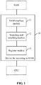
- Fig. 1 is a first schematic structure diagram of a device for accessing to a RAM according to a first embodiment of the disclosure. As shown in Fig. 1 , the device includes a register module 13, a searching and matching module 12, and an RAM interface module 11.
- the register module 13 is configured to acquire attribute information and startup information configured by a CPU and send the startup information to the searching and matching module 12, and also is used to store data information successfully matched by the searching and matching module 12 and instruct the CPU to read the data information.
- the searching and matching module 12 is configured to send address information to the RAM interface module 11 according to the startup information, and also is configured to acquire the data information sent by the RAM interface module 11, match the data information based on the attribute information in the register module 13 and send the data information to the register module 13 after matching is successful.
- the register module 13 is configured to acquire the attribute information and the startup information configured by the CPU.
- the attribute information includes to-be-accessed address range information.
- the searching and matching module 12 is used to send the address information to the RAM interface module 11 in sequence from a start address based on the to-be-accessed address range information after receiving the startup information.
- the register module 13 is configured to acquire the attribute information configured by the CPU.
- the attribute information includes an attribute parameter.
- the searching and matching module 12 is configured to match the data information based on the attribute parameter in the register module 13.
- the register module 13 is mainly configured to acquire the attribute information and the startup information configured by the CPU.
- the CPU may instruct the device for accessing the RAM in the embodiment on how to operate by configuring the attribute information, such as configuring an attribute parameter for matching, configuring a to-be-accessed RAM identifier (specifically RAM number), and configuring to-be-accessed RAM address range information (including a start address and an end address).
- the attribute information may include the attribute parameter, the RAM identifier and the RAM address range information, etc.
- the to-be-accessed RAM address range falls into the address range of the RAM.
- the to-be-accessed RAM address range is greater than or equal to a and is smaller than or equal to b, wherein a is greater than or equal to 0, b is smaller than or equal to N, and both a and b are the positive integer.
- the CPU configures the to-be-accessed address range information according to the RAM address range information.
- the to-be-accessed address range information is selectable, that is, the attribute information configured by the CPU acquired by the register module 13 also may exclude the to-be-accessed address range information.
- the searching and matching module sends the address information to the RAM interface module in sequence from an address 0 of the RAM to an address n (n characterizes a depth of the RAM) of the RAM.
- the CPU further may configure the startup information to instruct the device for accessing the RAM in the embodiment to start implementing data access.
- the CPU sends a signal that characterizes to implement the data access to the register module 13.
- the register module 13 starts to implement a data access operation based on the signal.
- the register module 13 is also used to acquire the data information successfully matched by the searching and matching module 12 and instruct the CPU that it may implement data reading.
- the searching and matching module 12 is configured to control addresses of the to-be-accessed RAM. Specifically, the searching and matching module 12 controls the RAM interface module 11 to read the data information from the corresponding RAM in sequence from the start address in the address range information based on the attribute information in the register module 13, specifically based on the address range information in the attribute information. After the data information of one piece of address information is read completely, the searching and matching module 12 enables an address value of the address information to add 1 to generate new address information, and sends the new address information to the RAM interface module 11 to continuously read the data information from the RAM until the data information corresponding to all address information in the address range information is read completely.
- the searching and matching module 12 matches the data information based on the attribute information of the register module 13. Specifically, the searching and matching module 12 matches the data information based on the attribute parameter in the register module 13 according to a preset matching rule.
- the preset matching rule includes whether to be equal to, smaller than or greater than the attribute parameter.
- the preset matching rule further may include whether to be equal to a preset threshold value after being operated according to a preset operational rule based on the attribute parameter.
- the PORT values of the matched data information are 8.
- the preset rule indicates to be smaller than the attribute parameter, the PORT values of the matched data information are smaller than 8. Accordingly, when the preset rule indicates to be greater than the attribute parameter, the PORT values of the matched data information are greater than 8.
- the preset rule indicates to be equal to the preset threshold value after being operated according to the preset operational rule based on the attribute parameter, it is assumed that the preset operational rule is a subtraction operation and the preset threshold value is 3, the PORT values of the matched data information are 5 or 11.
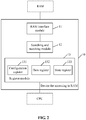
- Fig. 2 is a second schematic structure diagram of a device for accessing to a RAM according to a first embodiment of the disclosure.
- the register module 13 in the device for accessing to the RAM, includes a configuration register 131, a data register 132 and a state register 133.
- the configuration register 131 is configured to acquire the attribute information and the startup information configured by the CPU and send the startup information to the searching and matching module 12.
- the data register 132 is configured to store the data information successfully matched by the searching and matching module 12.
- the state register 133 is configured to instruct the CPU to read the data information.
- the CPU may instruct the device for accessing the RAM in the embodiment on how to operate by configuring the attribute information, such as, configuring the attribute parameter(s) for matching, configuring to-be-accessed RAM identifier(s) (specifically RAM number(s)), and configuring to-be-accessed RAM address range information (including a start address and an end address).
- the attribute information may include the attribute parameter(s), the RAM identifier(s) and the RAM address range information, etc.
- the configuration register 141 is configured to store the attribute information.
- the CPU further may configure the startup information to instruct the device for accessing to the RAM in the embodiment to start implementing data access.
- the CPU sends a signal that characterizes to implement the data access to the configuration register 131.
- the configuration register 131 sends the startup information to the searching and matching module 12 based on the signal.
- the data information successfully matched by the searching and matching module 12 is stored by the data register 132.
- the data information is stored in the data register 132, it is instructed by the state register 133 that the CPU may read the data information.
- the state register 133 is set into a high level so as to instruct that the CPU presently may read the data information.
- the configuration register 131 includes an attribute register and a startup register.
- the attribute register is configured to acquire the attribute information configured by the CPU.
- the startup register is configured to acquire the startup information configured by the CPU and send the startup information to the searching and matching module 12.
- the attribute register is configured to store the configured attribute information.
- the attribute information includes the attribute parameter(s), and further may include a to-be-accessed RAM identifier and to-be-accessed RAM address range information, etc.
- the startup register acquires the startup information configured by the CPU, and triggers the device for accessing the RAM in the embodiment to start implementing the data access based on the startup information configured by the CPU.
- the state register 133 includes a single-data acquired state register, configured to instruct the CPU to read the data information by a high level when the data information successfully matched by the searching and matching module is stored to the data register 132.
- the state register 133 further includes an all-data acquired state register, configured to instruct that the access to the RAM is ended when it is determined that the access to to-be-accessed data information ends.
- the searching and matching module 12 matches the data information read by the RAM based on the attribute information in the register module 13, and writes the data information successfully matched into the data register 132.
- the single-data acquired state register is set into the high level so as to instruct that the CPU may read the data information.
- the searching and matching module 12 determines that the address of the to-be-accessed RAM reaches to the end address, that is, after the last piece of data information to be accessed is written into the data register 132 and the CPU reads the last piece of data information, the all-data acquired state register is set into the high level so as to instruct that all to-be-accessed data information has been read and the access procedure is ended.
- the data information in conformity with the attribute information is matched internally through the device for accessing the RAM, and the data information is stored to the data register in the access device.
- the CPU only needs to access the register module (specifically, the state register and the data register in the register module) to directly read data in conformity with the attribute information, and the CPU is not required to traverse all data information in the RAM and then judge whether the data information meets the requirement of the attribute information. Therefore, the access time is greatly saved, and the access efficiency to the RAM is increased.
- the register module 13, the searching and matching module 12 and the RAM interface module 11 in the device for accessing the RAM all may be implemented by a Digital Signal Processor (DSP) or a Field-Programmable Gate Array (FPGA) in an actual application.
- DSP Digital Signal Processor
- FPGA Field-Programmable Gate Array
- Fig. 3 is a schematic structure diagram of a control chip according to a second embodiment of the disclosure. As shown in Fig. 3 , the control chip includes the RAM and the access devices for the RAM.
- the RAM is configured to store data information.
- the device for accessing the RAM includes the device for accessing the RAM in the first embodiment of the disclosure.
- control chip specifically may be an ASIC chip.
- the ASIC chip includes at least one RAM and the device for accessing the RAM in the embodiment of the disclosure. There is an interface with not too wide bandwidth between the device for accessing the RAM and the CPU, and the bandwidth is between 10M and 200M.
- the CPU is required to access the RAM in the ASIC via the interface whose bandwidth is not too wide, and the bandwidth is between 10M and 200M.
- the technical solutions of the embodiments of the disclosure are novel technical solutions on the premise of not changing the bandwidth of the original interface.
- the device for accessing the RAM includes a register module 13, a searching and matching module 12 and an RAM interface module 11.
- the register module 13 is configured to acquire attribute information and startup information configured by a CPU and send the startup information to the searching and matching module 12, and also is configured to store data information successfully matched by the searching and matching module 12 and instruct the CPU to read the data information.
- the searching and matching module 12 is configured to send address information to the RAM interface module 11 according to the startup information, and also is configured to acquire the data information sent by the RAM interface module 11, match the data information based on the attribute information in the register module 13 and send the data information to the register module 13 after matching is successful.
- the RAM interface module 11 is configured to read the data information from RAM based on the address information sent by the searching and matching module 12 and send the data information to the searching and matching module 12.
- the register module 13 is configured to acquire the attribute information and the startup information configured by the CPU.
- the attribute information includes to-be-accessed address range information.
- the searching and matching module 12 is configured to send the address information to the RAM interface module 11 in sequence from a start address based on the to-be-accessed address range information after receiving the startup information.
- the register module 13 is configured to acquire the attribute information configured by the CPU.
- the attribute information includes attribute parameter(s).
- the searching and matching module 12 is configured to match the data information based on the attribute parameter(s) in the register module 13.
- the register module 13 is mainly configured to acquire the attribute information and the startup information a configured by the CPU.
- the CPU may instruct the device for accessing to the RAM in the embodiment on how to operate by configuring the attribute information, such as configuring the attribute parameter(s) for matching, configuring to-be-accessed RAM identifier(s) (specifically RAM number(s)), and configuring to-be-accessed RAM address range information (including a start address and an end address).
- the attribute information may include the attribute parameter(s), the RAM identifier(s) and the RAM address range information, etc.
- the to-be-accessed RAM address range falls into address range of the RAM.
- the to-be-accessed RAM address range is greater than or equal to a and is smaller than or equal to b, wherein a is greater than or equal to 0, b is smaller than or equal to N, and both a and b are the positive integer.
- the CPU configures the to-be-accessed address range information according to the RAM address range information.
- the to-be-accessed address range information is selectable, that is, the attribute information configured by the CPU acquired by the register module 13 also may exclude the to-be-accessed address range information.
- the searching and matching module sends the address information to the RAM interface module in sequence from an address 0 of the RAM to an address n (n characterizes a depth of the RAM) of the RAM.
- the CPU further may configure the startup information to instruct the device for accessing to the RAM in the embodiment to start implementing data access.
- the CPU sends a signal that characterizes to implement the data access to the register module 13.
- the register module 13 starts to implement a data access operation based on the signal.
- the register module 13 is also configured to acquire the data information successfully matched by the searching and matching module 12 and instruct the CPU that it may implement data reading.
- the searching and matching module 12 is configured to control addresses of the to-be-accessed RAM. Specifically, the searching and matching module 12 controls the RAM interface module 11 to read the data information from the corresponding RAM in sequence from the start address in the address range information based on the attribute information in the register module 13, specifically based on the address range information in the attribute information. After the data information of one piece of address information is read completely, the searching and matching module 12 enables an address value of the address information to add 1 to generate new address information, and sends the new address information to the RAM interface module 11 to continuously read the data information from the RAM until the data information corresponding to all address information in the address range information is read completely.
- the searching and matching module 12 matches the data information based on the attribute information of the register module 13. Specifically, the searching and matching module 12 matches the data information according to a preset matching rule based on the attribute parameter in the register module 13.
- the preset matching rule includes whether to be equal to, smaller than or greater than the attribute parameter.
- the preset matching rule further may include whether to equal to a preset threshold value after being operated according to a preset operational rule based on the attribute parameter.
- the PORT values of the matched data information are 8.
- the preset rule indicates to be smaller than the attribute parameters
- the PORT values of the matched data information are smaller than 8.
- the PORT values of the matched data information are greater than 8.
- the preset rule indicates to be equal to the preset threshold value after being operated according to the preset operational rule based on the attribute parameter, it is assumed that the preset operational rule is a subtraction operation and the preset threshold value is 3, the PORT values of the matched data information are 5 or 11.
- the register module 13 includes a configuration register 131, a data register 132 and a state register 133.
- the configuration register 131 is configured to acquire the attribute information and the startup information configured by the CPU and send the startup information to the searching and matching module 12.
- the data register 132 is configured to store the data information successfully matched by the searching and matching module 12.
- the state register 133 is configured to instruct the CPU to read the data information.
- the CPU may instruct the device for accessing the RAM in the embodiment on how to operate by configuring the attribute information, such as configuring an attribute parameter for matching, configuring a to-be-accessed RAM identifier (specifically RAM number), and configuring to-be-accessed RAM address range information (including a start address and an end address).
- the attribute information may include the attribute parameter, the RAM identifier and the RAM address range information, etc.
- the configuration register 141 is used to store the attribute information.
- the CPU further may configure the startup information to instruct the device for accessing the RAM in the embodiment to start implementing data access.
- the CPU sends a signal that characterizes the data access to the configuration register 131.
- the configuration register 131 sends the startup information to the searching and matching module 12 based on the signal.
- the data information successfully matched by the searching and matching module 12 is stored by the data register 132.
- the data information is stored in the data register 132, it is instructed by the state register 133 that the CPU may read the data information.
- the state register 133 is set into a high level so as to instruct that the CPU presently may read the data information.
- the configuration register 131 includes an attribute register and a startup register.
- the attribute register is configured to acquire the attribute information configured by the CPU.
- the startup register is configured to acquire the startup information configured by the CPU and send the startup information to the searching and matching module 12.
- the attribute register is configured to store the configured attribute information.
- the attribute information includes the attribute parameter(s), and further may include to-be-accessed RAM identifier(s), and to-be-accessed RAM address range information, etc.
- the startup register acquires the startup information configured by the CPU, and triggers the device for accessing the RAM in the embodiment to start implementing the data access based on the startup information about the configuration of the CPU.
- the state register 133 further includes an all-data acquired state register, configured to instruct that the access to the RAM is ended when it is determined that the access to to-be-accessed data information ends.
- the searching and matching module 12 matches the data information read by the RAM based on the attribute information in the register module 13, and writes the data information successfully matched into the data register 132.
- the single-data acquired state register is set into the high level so as to instruct that the CPU may read the data information.
- the searching and matching module 12 determines that the addresses of the to-be-accessed RAM reach to the end address, that is, after the last piece of data information to be accessed is written into the data register 132 and the CPU reads the last piece of data information, the all-data acquired state register is set into the high level so as to instruct that all to-be-accessed data information has been read and the access procedure is ended.
- the data information in conformity with the attribute information is matched internally through the device for accessing the RAM, and the data information is stored to the data register in the access device.
- the CPU only needs to access the register module (specifically, the state register and the data register in the register module) to directly read data in conformity with the attribute information, and the CPU is not required to traverse all data information in the RAM and then judge whether the data information meets the requirement of the attribute information. Therefore, with the novel way for access to the RAM, the access time is greatly saved, and the access efficiency to the RAM is increased.
- the device for accessing the RAM in the embodiment may be implemented by a logic circuit in the control chip (specifically, it may be the ASIC chip), and the CPU is not required to match and screen the data information internally, so the access time is saved, and the access efficiency to the RAM is increased.
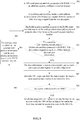
- Fig. 4 is a flowchart of a method for accessing to a RAM according to a third embodiment of the disclosure. As shown in Fig. 4 , the method comprises the following steps.
- step 401 attribute information and start information configured by a CPU are acquired.
- step 402 the RAM is searched based on the startup information and the attribute information to acquire data information.
- step 403 the data information is matched with the attribute information, and the CPU is instructed to read the data information after matching is successful.
- the attribute information includes to-be-accessed address range information and an attribute parameter.
- the operation that the RAM is searched based on the startup information and the attribute information to acquire the data information includes that the RAM is searched in sequence from a start address based on the address range information in the attribute information when the startup information configured by the CPU is received.
- the operation that the data information is matched with the attribute information includes that the data information is matched with the attribute parameter in the attribute information.
- the method for accessing to the RAM is applied to the device for accessing to the RAM. That is to say, an executive subject for the step 401 to the step 403 is the device for accessing to the RAM.
- the device for accessing to the RAM may be specifically referred to the description in the first embodiment or the second embodiment and will not be repeated herein.
- the operation that the attribute information configured by the CPU is acquired includes that a register module acquires the attribute information and the startup information configured by the CPU.
- the operation that the RAM is searched based on the attribute information and the startup information to acquire the data information includes that a searching and matching module sends address information to an RAM interface module based on the startup information; and the RAM interface module reads data information from the RAM based on the address information and sends the data information to the searching and matching module.
- the operation that the data information is matched with the attribute information and the CPU is instructed to read the data information after the matching is successful includes that the searching and matching module matches the data information based on the attribute information in the register module and sends the data information to the register module after the matching is successful; and the register module instructs the CPU to read the data information.
- an attribute register receives attribute information and startup information configured by a CPU.
- the attribute information includes one or more RAM numbers (RAM-ID(s)), and to-be-accessed start address and end address.
- a startup register sends a signal after receiving the startup information and triggers to start implementing an access process for the RAM.
- a searching and matching module sends the start address to an RAM interface module from the start address after receiving the signal of the startup register.
- the RAM interface module accesses the RAM according to the RAM number (RAM-ID), reads a data content corresponding to the start address from the RAM and sends the data content to the searching and matching module.
- the searching and matching module matches the information in the data content according to the attribute information in the attribute register.
- the matching is not successful, it enables an address value to add 1 to generate a new address and continuously sends the new address to the RAM interface module to read the data information until the read data information is matched successfully.
- the matching sends the data content to a data register and sets a single-data acquired state register into a high level so as to instruct that the CPU may read the data information and wait the CPU to read out the data information from the data register.
- step 4 when the CPU reads the data information in the data register, the searching and matching module continuously increases the address value (add 1 to the address value) and continuously sends the new address to the RAM interface module to read the data information, and the searching and matching module matches the read data content.
- the single-data acquired state register is set into a low level so as to instruct that the CPU presently has no data information to be read.
- the searching and matching module sends the data information successfully matched to the data register.
- step 5 the searching and matching module judges whether the address value reaches to an end address, thereby determining whether all data information successfully matched is read by the CPU.
- an all-data acquired state register is set into a high level so as to indicate that all data information has been read and to end the access operation to the RAM.
- the embodiment of the disclosure further provides a method for accessing to the RAM.
- the embodiment will be described in detail by a specific application.
- the control chip is the ASIC chip.
- the ASIC chip includes one RAM used to store an MAC address table.
- the depth of the RAM is 4096.
- the format of the RAM to store the data is as follows: ⁇ VLAN [11: 0], MAC [47: 0], PORT [11: 0] ⁇ . It is assumed that the PORT value of the data information to be read is 8.
- Fig. 5 is a flowchart of a method for accessing to a RAM according to a fourth embodiment of the disclosure. As shown in Fig. 5 , the method comprises the following steps.
- a searching and matching module sends address information (namely an address 0) to an RAM interface module from the address 0 after receiving a signal from the startup register.
- a default access address range in the embodiment includes all addresses of the RAM, namely, from the address 0 to the address 4096.
- step 503 the RAM interface module accesses to the RAM, reads data information of the address information (address 0) and sends the data information to the searching and matching module.
- step 506 the data information is sent to a data register, and a single-data acquired state register is set into a high level so as to instruct that the CPU may read the data information and wait the CPU to read out the data information from the data register. Further, when the CPU reads out the data information from the data register, the single-data acquired state register is set into a low level.
- step 507 after the CPU reads data from the data register, the single-data acquired state register is set into the low level.
- step 508 when the CPU reads the data in the data register, the searching and matching module determines whether the current address reaches to 4096 or not. If the current address does not reach to 4096, the step 503 is performed, namely, the searching and matching module enables the address value to add 1 to generate new address information and sends the new address information to the RAM interface module, and the step 503 is further performed again. If the current address reaches to 4096, the step 509 is performed.
- step 509 an all-data acquired state register is set into the high level, so as to notify the CPU of that all data information has been read out and the access procedure to the RAM is ended.
- the embodiments of the disclosure further provide a storage medium.
- a computer program is stored in the storage medium.
- the computer program is configured to implement the method for accessing the RAM in the foregoing embodiments.
- the elements described as separate components may be or may be not physically separated, and the components illustrated as elements may be or may be not physical elements, i.e., they may be located at one place or distributed in a plurality of network elements. Moreover, some of or all the elements may be selected according to actual demands to implement the purpose of the embodiments of the disclosure.
- the functional elements involved in the embodiments of the disclosure may be all integrated into a processing element or each of the elements may be act as a unit separately, or two or more than two of these elements may be integrated into one unit; the integrated element described above may be implemented in the form of hardware or may be implemented in the form of hardware plus software function elements.
- the integrated elements of the disclosure may be stored in a computer-readable storage medium.
- the technical solutions of the embodiments of the disclosure substantially or a part with contributions to the conventional art may be embodied in form of software product, and the computer software product is stored in a storage medium, including a plurality of instructions arranged to enable a computer (which may be a personal computer, a server, a network device or the like) to execute all or part of the method in each of the embodiments of the disclosure.
- the preceding storage medium includes various media capable of storing program codes such as a mobile storage device, an ROM, an RAM, a magnetic disk or a compact disc.
- the data information in conformity with the attribute information is matched internally through the device for accessing the RAM, and the data information is stored to the data register in the access device.
- the CPU only needs to access the register module to directly read data in conformity with the attribute information, and the CPU is not required to traverse all data information in the RAM and then judge whether the data information meets the requirement of the attribute information. Therefore, the access time is greatly saved, and the access efficiency to the RAM is increased.
Abstract
Description
- The disclosure relates to communications, and more particularly, to a method and device for accessing to a Random-Access Memory (RAM), a control chip and a storage medium.
- With the rapid development of a communication technology, a transmission rate of a network is developed to 100Gb/s or even higher. While the transmission rate is increased, there is an increasingly higher demand on an access speed to a RAM. For example, a routing table in a router and a Media/Medium Access Control (MAC) address table in a switch are stored in respective RAMs of corresponding communication devices. In order to know information stored in a RAM in real time, it is required to access to the RAM by a Central Processing Unit (CPU) and then perform the analysis. In the existing communication device, the data transmission at 100Gb/s or more is implemented by an Application Specific Integrated Circuit (ASIC) chip, while the RAM that stores such information as the routing table and the MAC address table is also positioned in this ASIC chip. In order to access to the RAM in the ASIC by the CPU, an interface is required. However, the bandwidth of the interface is not too wide, just between 10M and 200M.
- In the related art, the conventional access process to the RAM includes the following steps. Instructions such as an accessed RAM number (RAM-ID) and an access address are written into a command register by the CPU. A logic circuit inside the ASIC reads data information in the RAM according to the instructions in the command register. After the read data information is stored to a data register, the CPU reads the data information in the data register. In order to obtain the information in the RAM according to such a way, at least ten or more ASIC clock cycles are required to obtain one piece of the data information in the RAM. Furthermore, in order to obtain the information having a certain attribute in the RAM, under the condition that a specific address of the information in the RAM is not known, all addresses of the RAM are required to be traversed once and then the information having this attribute is extracted from all information in the RAM. In such a way, more time will be consumed to access to the RAM and the efficiency is relatively low.
- To solve the related technical problems, the embodiments of the disclosure provide a method and device for accessing to a RAM, a control chip and a storage medium that can solve the problem of low access efficiency to the RAM.
- The technical solutions of the embodiments of the disclosure are implemented as follows.
- The embodiments of the disclosure provide a device for accessing to a RAM. The device includes a register module, a searching and matching module and a RAM interface module.
- The register module is configured to acquire attribute information and startup information configured by a CPU and send the startup information to the searching and matching module, and also is configured to store data information successfully matched by the searching and matching module and instruct the CPU to read the data information.
- The searching and matching module is configured to send address information to the RAM interface module according to the startup information, and also is configured to acquire the data information sent by the RAM interface module, match the data information based on the attribute information in the register module and send the data information to the register module after matching is successful.
- The RAM interface module is configured to read the data information from RAM based on the address information sent by the searching and matching module and send the data information to the searching and matching module.
- In the above solutions, the register module is configured to acquire the attribute information and the startup information configured by the CPU. The attribute information includes to-be-accessed address range information.
- The searching and matching module is configured to send the address information to the RAM interface module in sequence from a start address to an end address based on the to-be-accessed address range information after receiving the startup information.
- In the above solutions, the register module is configured to acquire the attribute information configured by the CPU. The attribute information includes an attribute parameter.
- The searching and matching module is configured to match the data information based on the attribute parameter in the register module.
- In the above solutions, the register module includes a configuration register, a data register and a state register.
- The configuration register is configured to acquire the attribute information and the startup information about the configuration of the CPU and send the startup information to the searching and matching module.
- The data register is configured to store the data information successfully matched by the searching and matching module.
- The state register is configured to instruct the CPU to read the data information.
- In the above solutions, the configuration register includes an attribute register and a startup register.
- The attribute register is configured to acquire the attribute information configured by the CPU.
- The startup register is configured to acquire the startup information configured by the CPU and send the startup information to the searching and matching module.
- In the above solutions, the state register includes a single-data acquired state register, configured to instruct the CPU to read the data information by a high level when the data information successfully matched by the searching and matching module is stored to the data register.
- In the above solutions, the state register further includes an all-data acquired state register, configured to instruct that the access to the RAM is ended when it is determined that the access to to-be-accessed data information is ended.
- The embodiments of the disclosure further provide a method for accessing to the RAM. The method includes that attribute information and startup information configured by a CPU are acquired; the RAM is searched based on the startup information and the attribute information to acquire data information; and the data information is matched with the attribute information, and the CPU is instructed to read the data information after matching is successful.
- In the above solutions, the attribute information includes to-be-accessed address range information and an attribute parameter.
- The operation that the RAM is searched based on the startup information and the attribute information to acquire the data information includes the RAM is searched in sequence from a start address to an end address based on the address range information in the attribute information when the startup information configured by the CPU is received.
- Correspondingly, the operation that the data information is matched with the attribute information includes that the data information is matched with the attribute parameter in the attribute information.
- The embodiments of the disclosure further provide a control chip. The control chip includes a RAM as well as the device for accessing to the RAM according to any one of claims 1-7. The RAM is configured to store data information.
- The embodiments of the disclosure further provide a storage medium. A computer program is stored in the storage medium. The computer program is configured to implement the method for accessing to the RAM.
- According to the method and device for accessing to the RAM as well as the control chip provided by the embodiments of the disclosure, the data information in conformity with the attribute information is found internally through the device for accessing to the RAM, and the data information is stored to the data register in the access device. The CPU is only required to access to the register module (specifically, the state register and the data register in the register module) to directly read data in conformity with the attribute information, and the CPU is not required to traverse all data information in the RAM and then judge whether the data information meets the requirement of the attribute information. Therefore, the access time is greatly saved, and the access efficiency to the RAM is increased.
-
-
Fig. 1 is a first schematic structure diagram of a device for accessing to a RAM according to a first embodiment of the disclosure. -
Fig. 2 is a second schematic structure diagram of a device for accessing to a RAM according to a first embodiment of the disclosure. -
Fig. 3 is a schematic structure diagram of a control chip according to a second embodiment of the disclosure. -
Fig. 4 is a flowchart of a method for accessing to a RAM according to a third embodiment of the disclosure. -
Fig. 5 is a flowchart of a method for accessing to a RAM according to a fourth embodiment of the disclosure. - The disclosure will be further described below in detail with reference to accompanying drawings and specific embodiments.
- The embodiment of the disclosure provides a device for accessing to a RAM.
Fig. 1 is a first schematic structure diagram of a device for accessing to a RAM according to a first embodiment of the disclosure. As shown inFig. 1 , the device includes aregister module 13, a searching and matchingmodule 12, and anRAM interface module 11. - The
register module 13 is configured to acquire attribute information and startup information configured by a CPU and send the startup information to the searching and matchingmodule 12, and also is used to store data information successfully matched by the searching and matchingmodule 12 and instruct the CPU to read the data information. - The searching and matching
module 12 is configured to send address information to theRAM interface module 11 according to the startup information, and also is configured to acquire the data information sent by theRAM interface module 11, match the data information based on the attribute information in theregister module 13 and send the data information to theregister module 13 after matching is successful. - The
RAM interface module 11 is configured to read the data information from the RAM based on the address information sent by the searching and matchingmodule 12 and send the data information to the searching and matchingmodule 12. - Herein, the
register module 13 is configured to acquire the attribute information and the startup information configured by the CPU. The attribute information includes to-be-accessed address range information. The searching and matchingmodule 12 is used to send the address information to theRAM interface module 11 in sequence from a start address based on the to-be-accessed address range information after receiving the startup information. - Herein, the
register module 13 is configured to acquire the attribute information configured by the CPU. The attribute information includes an attribute parameter. The searching and matchingmodule 12 is configured to match the data information based on the attribute parameter in theregister module 13. - In the embodiment, the
register module 13 is mainly configured to acquire the attribute information and the startup information configured by the CPU. The CPU may instruct the device for accessing the RAM in the embodiment on how to operate by configuring the attribute information, such as configuring an attribute parameter for matching, configuring a to-be-accessed RAM identifier (specifically RAM number), and configuring to-be-accessed RAM address range information (including a start address and an end address). In other words, the attribute information may include the attribute parameter, the RAM identifier and the RAM address range information, etc. Herein, the to-be-accessed RAM address range falls into the address range of the RAM. Namely, when the address range of the RAM is greater or equal to 0 and is smaller than or equal to N (N is a positive integer), the to-be-accessed RAM address range is greater than or equal to a and is smaller than or equal to b, wherein a is greater than or equal to 0, b is smaller than or equal to N, and both a and b are the positive integer. It may be understood that, the CPU configures the to-be-accessed address range information according to the RAM address range information. Of course, the to-be-accessed address range information is selectable, that is, the attribute information configured by the CPU acquired by theregister module 13 also may exclude the to-be-accessed address range information. When the attribute information excludes the to-be-accessed address range information, the searching and matching module sends the address information to the RAM interface module in sequence from anaddress 0 of the RAM to an address n (n characterizes a depth of the RAM) of the RAM. Furthermore, the CPU further may configure the startup information to instruct the device for accessing the RAM in the embodiment to start implementing data access. Here, it also may be understood that, the CPU sends a signal that characterizes to implement the data access to theregister module 13. Theregister module 13 starts to implement a data access operation based on the signal. Theregister module 13 is also used to acquire the data information successfully matched by the searching and matchingmodule 12 and instruct the CPU that it may implement data reading. - The searching and matching
module 12 is configured to control addresses of the to-be-accessed RAM. Specifically, the searching and matchingmodule 12 controls theRAM interface module 11 to read the data information from the corresponding RAM in sequence from the start address in the address range information based on the attribute information in theregister module 13, specifically based on the address range information in the attribute information. After the data information of one piece of address information is read completely, the searching and matchingmodule 12 enables an address value of the address information to add 1 to generate new address information, and sends the new address information to theRAM interface module 11 to continuously read the data information from the RAM until the data information corresponding to all address information in the address range information is read completely. - The
RAM interface module 11 is mainly configured to access the RAM, access the RAM using the address information instructed by the searching and matchingmodule 12 to acquire corresponding data information, and send the data information to the searching and matchingmodule 12 to match. - In the embodiment, the searching and matching
module 12 matches the data information based on the attribute information of theregister module 13. Specifically, the searching and matchingmodule 12 matches the data information based on the attribute parameter in theregister module 13 according to a preset matching rule. Herein the preset matching rule includes whether to be equal to, smaller than or greater than the attribute parameter. The preset matching rule further may include whether to be equal to a preset threshold value after being operated according to a preset operational rule based on the attribute parameter. - Specifically, taken PORT=8 as an example of the attribute parameter, when the preset rule indicates to be equal to the attribute parameter, the PORT values of the matched data information are 8. When the preset rule indicates to be smaller than the attribute parameter, the PORT values of the matched data information are smaller than 8. Accordingly, when the preset rule indicates to be greater than the attribute parameter, the PORT values of the matched data information are greater than 8. When the preset rule indicates to be equal to the preset threshold value after being operated according to the preset operational rule based on the attribute parameter, it is assumed that the preset operational rule is a subtraction operation and the preset threshold value is 3, the PORT values of the matched data information are 5 or 11.
- As an implementation mode,
Fig. 2 is a second schematic structure diagram of a device for accessing to a RAM according to a first embodiment of the disclosure. As shown inFig. 2 , in the device for accessing to the RAM, theregister module 13 includes aconfiguration register 131, adata register 132 and astate register 133. - The
configuration register 131 is configured to acquire the attribute information and the startup information configured by the CPU and send the startup information to the searching and matchingmodule 12. - The data register 132 is configured to store the data information successfully matched by the searching and matching
module 12. - The
state register 133 is configured to instruct the CPU to read the data information. - Specifically, the CPU may instruct the device for accessing the RAM in the embodiment on how to operate by configuring the attribute information, such as, configuring the attribute parameter(s) for matching, configuring to-be-accessed RAM identifier(s) (specifically RAM number(s)), and configuring to-be-accessed RAM address range information (including a start address and an end address). In other words, the attribute information may include the attribute parameter(s), the RAM identifier(s) and the RAM address range information, etc. In the implementation mode, the configuration register 141 is configured to store the attribute information. On the other hand, the CPU further may configure the startup information to instruct the device for accessing to the RAM in the embodiment to start implementing data access. Here, it also may be understood that, the CPU sends a signal that characterizes to implement the data access to the
configuration register 131. Theconfiguration register 131 sends the startup information to the searching and matchingmodule 12 based on the signal. - In the implementation mode, the data information successfully matched by the searching and matching
module 12 is stored by the data register 132. When the data information is stored in the data register 132, it is instructed by thestate register 133 that the CPU may read the data information. Specifically, when the data information is stored in the data register 132, thestate register 133 is set into a high level so as to instruct that the CPU presently may read the data information. - Based on another implementation mode of the embodiment, the
configuration register 131 includes an attribute register and a startup register. - The attribute register is configured to acquire the attribute information configured by the CPU.
- The startup register is configured to acquire the startup information configured by the CPU and send the startup information to the searching and matching
module 12. - Specifically, the attribute register is configured to store the configured attribute information. The attribute information includes the attribute parameter(s), and further may include a to-be-accessed RAM identifier and to-be-accessed RAM address range information, etc. The startup register acquires the startup information configured by the CPU, and triggers the device for accessing the RAM in the embodiment to start implementing the data access based on the startup information configured by the CPU.
- Based on another implementation mode of the embodiment, the
state register 133 includes a single-data acquired state register, configured to instruct the CPU to read the data information by a high level when the data information successfully matched by the searching and matching module is stored to the data register 132. - The
state register 133 further includes an all-data acquired state register, configured to instruct that the access to the RAM is ended when it is determined that the access to to-be-accessed data information ends. - Specifically, the searching and matching
module 12 matches the data information read by the RAM based on the attribute information in theregister module 13, and writes the data information successfully matched into the data register 132. In this process, when there is the data information written into the data register 132, the single-data acquired state register is set into the high level so as to instruct that the CPU may read the data information. When the searching and matchingmodule 12 determines that the address of the to-be-accessed RAM reaches to the end address, that is, after the last piece of data information to be accessed is written into the data register 132 and the CPU reads the last piece of data information, the all-data acquired state register is set into the high level so as to instruct that all to-be-accessed data information has been read and the access procedure is ended. - According to the technical solution of the embodiment of the disclosure, under the condition that the bandwidth of the original interface is not changed, the data information in conformity with the attribute information is matched internally through the device for accessing the RAM, and the data information is stored to the data register in the access device. The CPU only needs to access the register module (specifically, the state register and the data register in the register module) to directly read data in conformity with the attribute information, and the CPU is not required to traverse all data information in the RAM and then judge whether the data information meets the requirement of the attribute information. Therefore, the access time is greatly saved, and the access efficiency to the RAM is increased.
- In the embodiment, the
register module 13, the searching and matchingmodule 12 and theRAM interface module 11 in the device for accessing the RAM all may be implemented by a Digital Signal Processor (DSP) or a Field-Programmable Gate Array (FPGA) in an actual application. - Based on the device for accessing the RAM in the first embodiment, the embodiment of the disclosure further provides a control chip.
Fig. 3 is a schematic structure diagram of a control chip according to a second embodiment of the disclosure. As shown inFig. 3 , the control chip includes the RAM and the access devices for the RAM. - The RAM is configured to store data information.
- The device for accessing the RAM includes the device for accessing the RAM in the first embodiment of the disclosure.
- In the embodiment, the control chip specifically may be an ASIC chip. The ASIC chip includes at least one RAM and the device for accessing the RAM in the embodiment of the disclosure. There is an interface with not too wide bandwidth between the device for accessing the RAM and the CPU, and the bandwidth is between 10M and 200M. However, in the conventional technical solutions, the CPU is required to access the RAM in the ASIC via the interface whose bandwidth is not too wide, and the bandwidth is between 10M and 200M. Hence, it may be understood that, the technical solutions of the embodiments of the disclosure are novel technical solutions on the premise of not changing the bandwidth of the original interface.
- Specifically, based on the embodiment herein and as shown in
Fig. 1 andFig. 2 , the device for accessing the RAM includes aregister module 13, a searching and matchingmodule 12 and anRAM interface module 11. - The
register module 13 is configured to acquire attribute information and startup information configured by a CPU and send the startup information to the searching and matchingmodule 12, and also is configured to store data information successfully matched by the searching and matchingmodule 12 and instruct the CPU to read the data information. - The searching and matching
module 12 is configured to send address information to theRAM interface module 11 according to the startup information, and also is configured to acquire the data information sent by theRAM interface module 11, match the data information based on the attribute information in theregister module 13 and send the data information to theregister module 13 after matching is successful. - The
RAM interface module 11 is configured to read the data information from RAM based on the address information sent by the searching and matchingmodule 12 and send the data information to the searching and matchingmodule 12. - Herein, the
register module 13 is configured to acquire the attribute information and the startup information configured by the CPU. The attribute information includes to-be-accessed address range information. The searching and matchingmodule 12 is configured to send the address information to theRAM interface module 11 in sequence from a start address based on the to-be-accessed address range information after receiving the startup information. - Herein, the
register module 13 is configured to acquire the attribute information configured by the CPU. The attribute information includes attribute parameter(s). The searching and matchingmodule 12 is configured to match the data information based on the attribute parameter(s) in theregister module 13. - In the embodiment, the
register module 13 is mainly configured to acquire the attribute information and the startup information a configured by the CPU. The CPU may instruct the device for accessing to the RAM in the embodiment on how to operate by configuring the attribute information, such as configuring the attribute parameter(s) for matching, configuring to-be-accessed RAM identifier(s) (specifically RAM number(s)), and configuring to-be-accessed RAM address range information (including a start address and an end address). In other words, the attribute information may include the attribute parameter(s), the RAM identifier(s) and the RAM address range information, etc. Herein, the to-be-accessed RAM address range falls into address range of the RAM. Namely, when the address range of the RAM is greater or equal to 0 and is smaller than or equal to N (N is a positive integer), the to-be-accessed RAM address range is greater than or equal to a and is smaller than or equal to b, wherein a is greater than or equal to 0, b is smaller than or equal to N, and both a and b are the positive integer. It may be understood that, the CPU configures the to-be-accessed address range information according to the RAM address range information. Of course, the to-be-accessed address range information is selectable, that is, the attribute information configured by the CPU acquired by theregister module 13 also may exclude the to-be-accessed address range information. When the attribute information excludes the to-be-accessed address range information, the searching and matching module sends the address information to the RAM interface module in sequence from anaddress 0 of the RAM to an address n (n characterizes a depth of the RAM) of the RAM. Furthermore, the CPU further may configure the startup information to instruct the device for accessing to the RAM in the embodiment to start implementing data access. Here, it also may be understood that, the CPU sends a signal that characterizes to implement the data access to theregister module 13. Theregister module 13 starts to implement a data access operation based on the signal. Theregister module 13 is also configured to acquire the data information successfully matched by the searching and matchingmodule 12 and instruct the CPU that it may implement data reading. - The searching and matching
module 12 is configured to control addresses of the to-be-accessed RAM. Specifically, the searching and matchingmodule 12 controls theRAM interface module 11 to read the data information from the corresponding RAM in sequence from the start address in the address range information based on the attribute information in theregister module 13, specifically based on the address range information in the attribute information. After the data information of one piece of address information is read completely, the searching and matchingmodule 12 enables an address value of the address information to add 1 to generate new address information, and sends the new address information to theRAM interface module 11 to continuously read the data information from the RAM until the data information corresponding to all address information in the address range information is read completely. - The
RAM interface module 11 is mainly configured to access the RAM, access the RAM using the address information instructed by the searching and matchingmodule 12 to acquire corresponding data information, and send the data information to the searching and matchingmodule 12 to match. - In the embodiment, the searching and matching
module 12 matches the data information based on the attribute information of theregister module 13. Specifically, the searching and matchingmodule 12 matches the data information according to a preset matching rule based on the attribute parameter in theregister module 13. The preset matching rule includes whether to be equal to, smaller than or greater than the attribute parameter. The preset matching rule further may include whether to equal to a preset threshold value after being operated according to a preset operational rule based on the attribute parameter. - Specifically, taken PORT=8 as an example of the attribute parameter, when the preset rule indicates to be equal to the attribute parameter, the PORT values of the matched data information are 8. When the preset rule indicates to be smaller than the attribute parameters, the PORT values of the matched data information are smaller than 8. Accordingly, when the preset rule indicates to be greater than the attribute parameter, the PORT values of the matched data information are greater than 8. When the preset rule indicates to be equal to the preset threshold value after being operated according to the preset operational rule based on the attribute parameter, it is assumed that the preset operational rule is a subtraction operation and the preset threshold value is 3, the PORT values of the matched data information are 5 or 11.
- As an implementation mode, as shown in
Fig. 2 , in the device for accessing the RAM, theregister module 13 includes aconfiguration register 131, adata register 132 and astate register 133. - The
configuration register 131 is configured to acquire the attribute information and the startup information configured by the CPU and send the startup information to the searching and matchingmodule 12. - The data register 132 is configured to store the data information successfully matched by the searching and matching
module 12. - The
state register 133 is configured to instruct the CPU to read the data information. - Specifically, the CPU may instruct the device for accessing the RAM in the embodiment on how to operate by configuring the attribute information, such as configuring an attribute parameter for matching, configuring a to-be-accessed RAM identifier (specifically RAM number), and configuring to-be-accessed RAM address range information (including a start address and an end address). In other words, the attribute information may include the attribute parameter, the RAM identifier and the RAM address range information, etc. In the implementation mode, the configuration register 141 is used to store the attribute information. On the other hand, the CPU further may configure the startup information to instruct the device for accessing the RAM in the embodiment to start implementing data access. Here, it also may be understood that, the CPU sends a signal that characterizes the data access to the
configuration register 131. Theconfiguration register 131 sends the startup information to the searching and matchingmodule 12 based on the signal. - In the implementation mode, the data information successfully matched by the searching and matching
module 12 is stored by the data register 132. When the data information is stored in the data register 132, it is instructed by thestate register 133 that the CPU may read the data information. Specifically, when the data information is stored in the data register 132, thestate register 133 is set into a high level so as to instruct that the CPU presently may read the data information. - Based on another implementation mode of the embodiment, the
configuration register 131 includes an attribute register and a startup register. - The attribute register is configured to acquire the attribute information configured by the CPU.
- The startup register is configured to acquire the startup information configured by the CPU and send the startup information to the searching and matching
module 12. - Specifically, the attribute register is configured to store the configured attribute information. The attribute information includes the attribute parameter(s), and further may include to-be-accessed RAM identifier(s), and to-be-accessed RAM address range information, etc. The startup register acquires the startup information configured by the CPU, and triggers the device for accessing the RAM in the embodiment to start implementing the data access based on the startup information about the configuration of the CPU.
- Based on another implementation mode of the embodiment, the
state register 133 includes a single-data acquired state register, configured to instruct the CPU to read the data information by a high level when the data information successfully matched by the searching and matching module is stored to the data register 132. - The
state register 133 further includes an all-data acquired state register, configured to instruct that the access to the RAM is ended when it is determined that the access to to-be-accessed data information ends. - Specifically, the searching and matching
module 12 matches the data information read by the RAM based on the attribute information in theregister module 13, and writes the data information successfully matched into the data register 132. In this process, when there is the data information written into the data register 132, the single-data acquired state register is set into the high level so as to instruct that the CPU may read the data information. When the searching and matchingmodule 12 determines that the addresses of the to-be-accessed RAM reach to the end address, that is, after the last piece of data information to be accessed is written into the data register 132 and the CPU reads the last piece of data information, the all-data acquired state register is set into the high level so as to instruct that all to-be-accessed data information has been read and the access procedure is ended. - To sum up, according to the embodiments of the disclosure, under the condition that the bandwidth of the original interface is not changed, the data information in conformity with the attribute information is matched internally through the device for accessing the RAM, and the data information is stored to the data register in the access device. The CPU only needs to access the register module (specifically, the state register and the data register in the register module) to directly read data in conformity with the attribute information, and the CPU is not required to traverse all data information in the RAM and then judge whether the data information meets the requirement of the attribute information. Therefore, with the novel way for access to the RAM, the access time is greatly saved, and the access efficiency to the RAM is increased. Furthermore, the device for accessing the RAM in the embodiment may be implemented by a logic circuit in the control chip (specifically, it may be the ASIC chip), and the CPU is not required to match and screen the data information internally, so the access time is saved, and the access efficiency to the RAM is increased.
- Based on the first embodiment or the second embodiment, the embodiment of the disclosure further provides a method for accessing to the RAM.
Fig. 4 is a flowchart of a method for accessing to a RAM according to a third embodiment of the disclosure. As shown inFig. 4 , the method comprises the following steps. - In
step 401, attribute information and start information configured by a CPU are acquired. - In
step 402, the RAM is searched based on the startup information and the attribute information to acquire data information. - In
step 403, the data information is matched with the attribute information, and the CPU is instructed to read the data information after matching is successful. - Specifically, the attribute information includes to-be-accessed address range information and an attribute parameter.
- The operation that the RAM is searched based on the startup information and the attribute information to acquire the data information includes that the RAM is searched in sequence from a start address based on the address range information in the attribute information when the startup information configured by the CPU is received.
- Accordingly, the operation that the data information is matched with the attribute information includes that the data information is matched with the attribute parameter in the attribute information.
- In the embodiment, the method for accessing to the RAM is applied to the device for accessing to the RAM. That is to say, an executive subject for the
step 401 to thestep 403 is the device for accessing to the RAM. The device for accessing to the RAM may be specifically referred to the description in the first embodiment or the second embodiment and will not be repeated herein. - Specifically, in the
step 401, the operation that the attribute information configured by the CPU is acquired includes that a register module acquires the attribute information and the startup information configured by the CPU. In thestep 402, the operation that the RAM is searched based on the attribute information and the startup information to acquire the data information includes that a searching and matching module sends address information to an RAM interface module based on the startup information; and the RAM interface module reads data information from the RAM based on the address information and sends the data information to the searching and matching module. In thestep 403, the operation that the data information is matched with the attribute information and the CPU is instructed to read the data information after the matching is successful includes that the searching and matching module matches the data information based on the attribute information in the register module and sends the data information to the register module after the matching is successful; and the register module instructs the CPU to read the data information. - The method for accessing to the RAM in the embodiment of the disclosure will be described below in detail with reference to the specific embodiment based on the device for accessing the RAM shown in
Fig. 2 . - In step 1, an attribute register receives attribute information and startup information configured by a CPU. The attribute information includes one or more RAM numbers (RAM-ID(s)), and to-be-accessed start address and end address. A startup register sends a signal after receiving the startup information and triggers to start implementing an access process for the RAM.
- In step 2, a searching and matching module sends the start address to an RAM interface module from the start address after receiving the signal of the startup register.
- In step 3, the RAM interface module accesses the RAM according to the RAM number (RAM-ID), reads a data content corresponding to the start address from the RAM and sends the data content to the searching and matching module. The searching and matching module matches the information in the data content according to the attribute information in the attribute register. When the matching is not successful, it enables an address value to add 1 to generate a new address and continuously sends the new address to the RAM interface module to read the data information until the read data information is matched successfully. When the matching is successful, it sends the data content to a data register and sets a single-data acquired state register into a high level so as to instruct that the CPU may read the data information and wait the CPU to read out the data information from the data register.
- In step 4, when the CPU reads the data information in the data register, the searching and matching module continuously increases the address value (add 1 to the address value) and continuously sends the new address to the RAM interface module to read the data information, and the searching and matching module matches the read data content. After the CPU reads the data in the data register completely, the single-data acquired state register is set into a low level so as to instruct that the CPU presently has no data information to be read. The searching and matching module sends the data information successfully matched to the data register.
- In step 5, the searching and matching module judges whether the address value reaches to an end address, thereby determining whether all data information successfully matched is read by the CPU. When the address value reaches to the end address, an all-data acquired state register is set into a high level so as to indicate that all data information has been read and to end the access operation to the RAM.
- The embodiment of the disclosure further provides a method for accessing to the RAM. The embodiment will be described in detail by a specific application. In the embodiment, it is assumed that the control chip is the ASIC chip. The ASIC chip includes one RAM used to store an MAC address table. The depth of the RAM is 4096. The format of the RAM to store the data is as follows: {VLAN [11: 0], MAC [47: 0], PORT [11: 0]}. It is assumed that the PORT value of the data information to be read is 8.
Fig. 5 is a flowchart of a method for accessing to a RAM according to a fourth embodiment of the disclosure. As shown inFig. 5 , the method comprises the following steps. - In step 501, a CPU configures an attribute parameter with PORT = 8 into an attribute register, configures a startup register and triggers to start implementing an access process to the RAM.
- In
step 502, a searching and matching module sends address information (namely an address 0) to an RAM interface module from theaddress 0 after receiving a signal from the startup register. - In the embodiment, since the attribute information configured by the CPU does not include a start address and an end address, a default access address range in the embodiment includes all addresses of the RAM, namely, from the
address 0 to theaddress 4096. - In
step 503, the RAM interface module accesses to the RAM, reads data information of the address information (address 0) and sends the data information to the searching and matching module. - In
step 504, the searching and matching module determines whether the attribute parameter with PORT = 8 in the attribute register is equal to a PORT field of the read data information or not. If no, thestep 505 is performed, namely, the searching and matching module enables the address value to add 1 to generate new address information and sends the address information to the RAM interface module. Furthermore, thestep 503 is further performed again until the matching is successful. If the attribute parameter with PORT = 8 in the attribute register is equal to a PORT field of the read data information, thestep 506 is performed. - In
step 506, the data information is sent to a data register, and a single-data acquired state register is set into a high level so as to instruct that the CPU may read the data information and wait the CPU to read out the data information from the data register. Further, when the CPU reads out the data information from the data register, the single-data acquired state register is set into a low level. - In
step 507, after the CPU reads data from the data register, the single-data acquired state register is set into the low level. - In
step 508, when the CPU reads the data in the data register, the searching and matching module determines whether the current address reaches to 4096 or not. If the current address does not reach to 4096, thestep 503 is performed, namely, the searching and matching module enables the address value to add 1 to generate new address information and sends the new address information to the RAM interface module, and thestep 503 is further performed again. If the current address reaches to 4096, thestep 509 is performed. - In
step 509, an all-data acquired state register is set into the high level, so as to notify the CPU of that all data information has been read out and the access procedure to the RAM is ended. - The embodiments of the disclosure further provide a storage medium. A computer program is stored in the storage medium. The computer program is configured to implement the method for accessing the RAM in the foregoing embodiments.
- In the several embodiments provided in the disclosure, it should be understood that the devices and methods disclosed can be implemented in other ways. The device embodiments described above are merely exemplary. For example, the division of the elements is merely a division based on logic functions, and in practice, there are other division ways. For example, some of the elements or components may be combined or integrated into other system, or some features may be omitted or unexecuted. Moreover, coupling or direct coupling or communication connection between the components illustrated or discussed herein may be indirect coupling or communication connection between devices or elements by some interfaces or may be electric connection, mechanical connection or the other forms of connection.
- The elements described as separate components may be or may be not physically separated, and the components illustrated as elements may be or may be not physical elements, i.e., they may be located at one place or distributed in a plurality of network elements. Moreover, some of or all the elements may be selected according to actual demands to implement the purpose of the embodiments of the disclosure.
- In addition, the functional elements involved in the embodiments of the disclosure may be all integrated into a processing element or each of the elements may be act as a unit separately, or two or more than two of these elements may be integrated into one unit; the integrated element described above may be implemented in the form of hardware or may be implemented in the form of hardware plus software function elements.
- It should be understood by those ordinary skilled in the art that all or some of the steps of the foregoing method embodiments can be implemented by program instruction related hardware. The program described above may be stored in a computer-readable storage medium. The program, when executed, executes the steps of the method embodiments described above. The storage medium described above includes a mobile hard disk drive, a Read-Only Memory (ROM), a Random Access Memory (RAM), a disk, a compact disc or another medium capable of storing program codes.
- Alternatively, if being implemented in form of a software function module and sold or used as an independent product, the integrated elements of the disclosure may be stored in a computer-readable storage medium. Based on such an understanding, the technical solutions of the embodiments of the disclosure substantially or a part with contributions to the conventional art may be embodied in form of software product, and the computer software product is stored in a storage medium, including a plurality of instructions arranged to enable a computer (which may be a personal computer, a server, a network device or the like) to execute all or part of the method in each of the embodiments of the disclosure. The preceding storage medium includes various media capable of storing program codes such as a mobile storage device, an ROM, an RAM, a magnetic disk or a compact disc.
- The above description is only specific embodiments of the disclosure and the protection scope of the disclosure is not limited to this. It may be readily conceivable for those skilled in the art to have changes or modifications in the technical scope of the disclosure, and all of the changes or modifications should fall within the protection scope of the disclosure. Therefore, the protection scope of the disclosure should be accordance with the protection scope of the appended claims.
- According to the disclosure, the data information in conformity with the attribute information is matched internally through the device for accessing the RAM, and the data information is stored to the data register in the access device. The CPU only needs to access the register module to directly read data in conformity with the attribute information, and the CPU is not required to traverse all data information in the RAM and then judge whether the data information meets the requirement of the attribute information. Therefore, the access time is greatly saved, and the access efficiency to the RAM is increased.
Claims (11)
- A device for accessing to a Random Access Memory (RAM), comprising: a register module, a searching and matching module, and a RAM interface module, wherein
the register module is configured to acquire attribute information and startup information configured by a Central Processing Unit (CPU), send the startup information to the searching and matching module, store data information successfully matched by the searching and matching module and instruct the CPU to read the data information;
the searching and matching module is configured to send address information to the RAM interface module according to the startup information, acquire the data information sent by the RAM interface module, match the data information based on the attribute information in the register module and send the data information to the register module after matching is successful; and
the RAM interface module is configured to read the data information from the RAM based on the address information sent by the searching and matching module and send the data information to the searching and matching module. - The device according to claim 1, wherein the register module is configured to acquire the attribute information and the startup information configured by the CPU;
the attribute information comprises to-be-accessed address range information; and
the searching and matching module is configured to send the address information to the RAM interface module in sequence from a start address to an end address based on the to-be-accessed address range information after receiving the startup information. - The device according to claim 1, wherein the register module is configured to acquire the attribute information configured by the CPU;
the attribute information comprises an attribute parameter; and
the searching and matching module is configured to match the data information based on the attribute parameter in the register module. - The device according to claim 1, wherein the register module comprises a configuration register, a data register and a state register;
the configuration register is configured to acquire the attribute information and the startup information configured by the CPU and send the startup information to the searching and matching module;
the data register is configured to store the data information successfully matched by the searching and matching module; and
the state register is configured to instruct the CPU to read the data information. - The device according to claim 4, wherein the configuration register comprises an attribute register and a startup register;
the attribute register is configured to acquire the attribute information configured by the CPU; and
the startup register is configured to acquire the startup information configured by the CPU and send the startup information to the searching and matching module. - The device according to claim 4, wherein the state register comprises a single-data acquired state register, configured to instruct the CPU to read the data information by a high level when the data information successfully matched by the searching and matching module is stored to the data register.
- The device according to claim 6, wherein the state register further comprises an all-data acquired state register, configured to instruct that the access to the RAM is ended when it is determined that the access to to-be-accessed data information is ended.
- A method for accessing to a Random Access Memory (RAM), comprising:acquiring attribute information and startup information configured by a Central Processing Unit (CPU);searching for the RAM based on the startup information and the attribute information to acquire data information; andmatching the data information with the attribute information and instructing the CPU to read the data information after matching is successful.
- The method according to claim 8, wherein the attribute information comprises to-be-accessed address range information and an attribute parameter;
said searching for the RAM based on the startup information and the attribute information to acquire the data information comprises: searching for the RAM in sequence from a start address to an end address based on the address range information in the attribute information when the startup information configured by the CPU is received; and
said matching the data information with the attribute information comprises:matching the data information with the attribute parameter in the attribute information. - A control chip, comprising a Random-Access Memory (RAM) and the device for accessing to the RAM according to any one of claims 1 to 7, wherein
the RAM is configured to store data information. - A storage medium having a computer program stored therein, wherein the computer program is configured to implement the method for accessing to the Random-Access Memory (RAM) according to claim 8 or 9.
Applications Claiming Priority (2)
| Application Number | Priority Date | Filing Date | Title |
|---|---|---|---|
| CN201510336814.7A CN104965676B (en) | 2015-06-17 | 2015-06-17 | A kind of access method of random access memory, device and control chip |
| PCT/CN2016/085501 WO2016202222A1 (en) | 2015-06-17 | 2016-06-12 | Access method and device for random access memories, control chip and storage medium |
Publications (3)
| Publication Number | Publication Date |
|---|---|
| EP3285159A1 true EP3285159A1 (en) | 2018-02-21 |
| EP3285159A4 EP3285159A4 (en) | 2018-03-28 |
| EP3285159B1 EP3285159B1 (en) | 2020-09-16 |
Family
ID=54219711
Family Applications (1)
| Application Number | Title | Priority Date | Filing Date |
|---|---|---|---|
| EP16810963.5A Active EP3285159B1 (en) | 2015-06-17 | 2016-06-12 | Access method and device for random access memories, control chip and storage medium |
Country Status (4)
| Country | Link |
|---|---|
| US (1) | US10552068B2 (en) |
| EP (1) | EP3285159B1 (en) |
| CN (1) | CN104965676B (en) |
| WO (1) | WO2016202222A1 (en) |
Families Citing this family (6)
| Publication number | Priority date | Publication date | Assignee | Title |
|---|---|---|---|---|
| CN104965676B (en) * | 2015-06-17 | 2018-10-16 | 深圳市中兴微电子技术有限公司 | A kind of access method of random access memory, device and control chip |
| CN106126114B (en) * | 2016-06-15 | 2018-09-07 | 武汉卡码酷科技有限公司 | A kind of memory and its querying method having query function |
| CN109408406B (en) * | 2018-10-18 | 2023-02-14 | 深圳三地一芯电子有限责任公司 | Data storage method and storage medium of flash memory |
| CN110095683A (en) * | 2019-04-12 | 2019-08-06 | 华勤通讯技术有限公司 | A kind of equipment detection method and device |
| CN111224877A (en) * | 2019-12-10 | 2020-06-02 | 中国航空工业集团公司西安航空计算技术研究所 | VL query method and device of AFDX switch |
| CN114217744A (en) * | 2021-12-14 | 2022-03-22 | 山东产研鲲云人工智能研究院有限公司 | EFUSE storage content distribution method and device using shadow register |
Family Cites Families (16)
| Publication number | Priority date | Publication date | Assignee | Title |
|---|---|---|---|---|
| US5283882A (en) | 1991-02-22 | 1994-02-01 | Unisys Corporation | Data caching and address translation system with rapid turnover cycle |
| JPH09319665A (en) | 1996-05-30 | 1997-12-12 | Nec Corp | Data backup system for writable/readable non-volatile memory |
| US6701432B1 (en) | 1999-04-01 | 2004-03-02 | Netscreen Technologies, Inc. | Firewall including local bus |
| CN1450457A (en) | 2003-04-16 | 2003-10-22 | 复旦大学 | Low power dissipation group associated cache memory adopting improved time sequency |
| CN100372317C (en) | 2005-05-13 | 2008-02-27 | 清华大学 | Flow receiving taking and statistic circuit assembly for 10G network performance tester |
| US20070288690A1 (en) * | 2006-06-13 | 2007-12-13 | Foundry Networks, Inc. | High bandwidth, high capacity look-up table implementation in dynamic random access memory |
| US9141572B2 (en) | 2006-12-15 | 2015-09-22 | Microchip Technology Incorporated | Direct memory access controller |
| JP4800415B2 (en) * | 2009-08-17 | 2011-10-26 | 富士通株式会社 | Relay device and MAC address search method |
| CN101651810B (en) | 2009-09-22 | 2011-01-05 | 西安交通大学 | Device and method for processing interlaced line-crossing stereoscopic composite video signals |
| CN102013274B (en) * | 2010-11-10 | 2013-08-07 | 无锡中星微电子有限公司 | Self-test circuit and method for storage |
| CN102608874A (en) | 2012-02-09 | 2012-07-25 | 合肥芯硕半导体有限公司 | Method for increasing data transmission speed of digital micromirror array by photoetching machine under scanning work mode |
| CN102866963B (en) * | 2012-09-18 | 2015-07-22 | 广西柳工机械股份有限公司 | Data storage and reading method for controller |
| US9110677B2 (en) | 2013-03-14 | 2015-08-18 | Sandisk Technologies Inc. | System and method for predicting and improving boot-up sequence |
| US9276846B2 (en) * | 2013-03-15 | 2016-03-01 | Cavium, Inc. | Packet extraction optimization in a network processor |
| CN103677758A (en) | 2013-10-18 | 2014-03-26 | 陕西高新实业有限公司 | Method for efficiently and concurrently operating software management layer and hardware management layer of chip |
| CN104965676B (en) * | 2015-06-17 | 2018-10-16 | 深圳市中兴微电子技术有限公司 | A kind of access method of random access memory, device and control chip |
-
2015
- 2015-06-17 CN CN201510336814.7A patent/CN104965676B/en active Active
-
2016
- 2016-06-12 EP EP16810963.5A patent/EP3285159B1/en active Active
- 2016-06-12 WO PCT/CN2016/085501 patent/WO2016202222A1/en active Application Filing
- 2016-06-12 US US15/571,189 patent/US10552068B2/en active Active
Also Published As
| Publication number | Publication date |
|---|---|
| EP3285159B1 (en) | 2020-09-16 |
| WO2016202222A1 (en) | 2016-12-22 |
| US20180267727A1 (en) | 2018-09-20 |
| US10552068B2 (en) | 2020-02-04 |
| EP3285159A4 (en) | 2018-03-28 |
| CN104965676A (en) | 2015-10-07 |
| CN104965676B (en) | 2018-10-16 |
Similar Documents
| Publication | Publication Date | Title |
|---|---|---|
| US10552068B2 (en) | Access method and device for random access memories, control chip and storage medium | |
| WO2016188240A1 (en) | Method and device for configuring multiple network cards | |
| CN109634718B (en) | Method and system for creating mirror image by cloud platform | |
| US9253275B2 (en) | Cognitive dynamic allocation in caching appliances | |
| WO2015070640A1 (en) | Remote accessing method for device, thin client, and virtual machine | |
| CN108924274B (en) | Domain name system DNS processing method and device, storage medium and electronic equipment | |
| US9720755B2 (en) | Information processing device | |
| WO2020113478A1 (en) | Address information processing method and apparatus, electronic device, and storage medium | |
| US11126457B2 (en) | Method for batch processing nginx network isolation spaces and nginx server | |
| CN110753040B (en) | Request processing method and device | |
| US11301436B2 (en) | File storage method and storage apparatus | |
| US10057291B1 (en) | Comparing networking access control lists | |
| CN115039082A (en) | Log writing method and device, electronic equipment and storage medium | |
| CN109933479B (en) | Fault simulation and emulation method and related equipment | |
| CN114157633B (en) | Message forwarding method and device | |
| CN116361106A (en) | Log processing method and device, electronic equipment and storage medium | |
| CN115495406A (en) | Message transmission method, device, equipment and storage medium based on PCIe | |
| CN115604070A (en) | Message transmission method, device, equipment and medium based on MCTP (Multi-function peripheral protocol) | |
| CN112291212B (en) | Static rule management method and device, electronic equipment and storage medium | |
| CN111885664B (en) | User equipment routing method and related product | |
| CN113918423A (en) | Cloud platform monitoring method and device and application thereof | |
| CN109189339B (en) | Automatic configuration cache acceleration method under storage system | |
| EP3737066A1 (en) | Method for processing nginx network isolation spaces in batches and nginx server | |
| CN111625302A (en) | Function time consumption tracking method, device and storage medium | |
| CN117194388B (en) | Data management method, device, electronic equipment and storage medium |
Legal Events
| Date | Code | Title | Description |
|---|---|---|---|
| STAA | Information on the status of an ep patent application or granted ep patent |
Free format text: STATUS: THE INTERNATIONAL PUBLICATION HAS BEEN MADE |
|
| PUAI | Public reference made under article 153(3) epc to a published international application that has entered the european phase |
Free format text: ORIGINAL CODE: 0009012 |
|
| STAA | Information on the status of an ep patent application or granted ep patent |
Free format text: STATUS: REQUEST FOR EXAMINATION WAS MADE |
|
| 17P | Request for examination filed |
Effective date: 20171114 |
|
| AK | Designated contracting states |
Kind code of ref document: A1 Designated state(s): AL AT BE BG CH CY CZ DE DK EE ES FI FR GB GR HR HU IE IS IT LI LT LU LV MC MK MT NL NO PL PT RO RS SE SI SK SM TR |
|
| AX | Request for extension of the european patent |
Extension state: BA ME |
|
| A4 | Supplementary search report drawn up and despatched |
Effective date: 20180228 |
|
| RIC1 | Information provided on ipc code assigned before grant |
Ipc: G06F 3/06 20060101AFI20180222BHEP Ipc: H04L 12/741 20130101ALI20180222BHEP |
|
| DAV | Request for validation of the european patent (deleted) | ||
| DAX | Request for extension of the european patent (deleted) | ||
| STAA | Information on the status of an ep patent application or granted ep patent |
Free format text: STATUS: EXAMINATION IS IN PROGRESS |
|
| 17Q | First examination report despatched |
Effective date: 20181212 |
|
| REG | Reference to a national code |
Ref country code: DE Ref legal event code: R079 Ref document number: 602016044217 Country of ref document: DE Free format text: PREVIOUS MAIN CLASS: G06F0003060000 Ipc: G06F0013160000 |
|
| GRAP | Despatch of communication of intention to grant a patent |
Free format text: ORIGINAL CODE: EPIDOSNIGR1 |
|
| STAA | Information on the status of an ep patent application or granted ep patent |
Free format text: STATUS: GRANT OF PATENT IS INTENDED |
|
| RIC1 | Information provided on ipc code assigned before grant |
Ipc: G06F 13/16 20060101AFI20200624BHEP Ipc: G06F 3/06 20060101ALI20200624BHEP |
|
| GRAS | Grant fee paid |
Free format text: ORIGINAL CODE: EPIDOSNIGR3 |
|
| GRAA | (expected) grant |
Free format text: ORIGINAL CODE: 0009210 |
|
| STAA | Information on the status of an ep patent application or granted ep patent |
Free format text: STATUS: THE PATENT HAS BEEN GRANTED |
|
| INTG | Intention to grant announced |
Effective date: 20200721 |
|
| AK | Designated contracting states |
Kind code of ref document: B1 Designated state(s): AL AT BE BG CH CY CZ DE DK EE ES FI FR GB GR HR HU IE IS IT LI LT LU LV MC MK MT NL NO PL PT RO RS SE SI SK SM TR |
|
| REG | Reference to a national code |
Ref country code: GB Ref legal event code: FG4D |
|
| REG | Reference to a national code |
Ref country code: CH Ref legal event code: EP |
|
| REG | Reference to a national code |
Ref country code: DE Ref legal event code: R096 Ref document number: 602016044217 Country of ref document: DE |
|
| REG | Reference to a national code |
Ref country code: IE Ref legal event code: FG4D |
|
| REG | Reference to a national code |
Ref country code: AT Ref legal event code: REF Ref document number: 1314761 Country of ref document: AT Kind code of ref document: T Effective date: 20201015 |
|
| PG25 | Lapsed in a contracting state [announced via postgrant information from national office to epo] |
Ref country code: SE Free format text: LAPSE BECAUSE OF FAILURE TO SUBMIT A TRANSLATION OF THE DESCRIPTION OR TO PAY THE FEE WITHIN THE PRESCRIBED TIME-LIMIT Effective date: 20200916 Ref country code: BG Free format text: LAPSE BECAUSE OF FAILURE TO SUBMIT A TRANSLATION OF THE DESCRIPTION OR TO PAY THE FEE WITHIN THE PRESCRIBED TIME-LIMIT Effective date: 20201216 Ref country code: FI Free format text: LAPSE BECAUSE OF FAILURE TO SUBMIT A TRANSLATION OF THE DESCRIPTION OR TO PAY THE FEE WITHIN THE PRESCRIBED TIME-LIMIT Effective date: 20200916 Ref country code: GR Free format text: LAPSE BECAUSE OF FAILURE TO SUBMIT A TRANSLATION OF THE DESCRIPTION OR TO PAY THE FEE WITHIN THE PRESCRIBED TIME-LIMIT Effective date: 20201217 Ref country code: NO Free format text: LAPSE BECAUSE OF FAILURE TO SUBMIT A TRANSLATION OF THE DESCRIPTION OR TO PAY THE FEE WITHIN THE PRESCRIBED TIME-LIMIT Effective date: 20201216 Ref country code: HR Free format text: LAPSE BECAUSE OF FAILURE TO SUBMIT A TRANSLATION OF THE DESCRIPTION OR TO PAY THE FEE WITHIN THE PRESCRIBED TIME-LIMIT Effective date: 20200916 |
|
| REG | Reference to a national code |
Ref country code: AT Ref legal event code: MK05 Ref document number: 1314761 Country of ref document: AT Kind code of ref document: T Effective date: 20200916 |
|
| REG | Reference to a national code |
Ref country code: NL Ref legal event code: MP Effective date: 20200916 |
|
| PG25 | Lapsed in a contracting state [announced via postgrant information from national office to epo] |
Ref country code: RS Free format text: LAPSE BECAUSE OF FAILURE TO SUBMIT A TRANSLATION OF THE DESCRIPTION OR TO PAY THE FEE WITHIN THE PRESCRIBED TIME-LIMIT Effective date: 20200916 Ref country code: LV Free format text: LAPSE BECAUSE OF FAILURE TO SUBMIT A TRANSLATION OF THE DESCRIPTION OR TO PAY THE FEE WITHIN THE PRESCRIBED TIME-LIMIT Effective date: 20200916 |
|
| REG | Reference to a national code |
Ref country code: LT Ref legal event code: MG4D |
|
| PG25 | Lapsed in a contracting state [announced via postgrant information from national office to epo] |
Ref country code: LT Free format text: LAPSE BECAUSE OF FAILURE TO SUBMIT A TRANSLATION OF THE DESCRIPTION OR TO PAY THE FEE WITHIN THE PRESCRIBED TIME-LIMIT Effective date: 20200916 Ref country code: CZ Free format text: LAPSE BECAUSE OF FAILURE TO SUBMIT A TRANSLATION OF THE DESCRIPTION OR TO PAY THE FEE WITHIN THE PRESCRIBED TIME-LIMIT Effective date: 20200916 Ref country code: RO Free format text: LAPSE BECAUSE OF FAILURE TO SUBMIT A TRANSLATION OF THE DESCRIPTION OR TO PAY THE FEE WITHIN THE PRESCRIBED TIME-LIMIT Effective date: 20200916 Ref country code: PT Free format text: LAPSE BECAUSE OF FAILURE TO SUBMIT A TRANSLATION OF THE DESCRIPTION OR TO PAY THE FEE WITHIN THE PRESCRIBED TIME-LIMIT Effective date: 20210118 Ref country code: EE Free format text: LAPSE BECAUSE OF FAILURE TO SUBMIT A TRANSLATION OF THE DESCRIPTION OR TO PAY THE FEE WITHIN THE PRESCRIBED TIME-LIMIT Effective date: 20200916 Ref country code: SM Free format text: LAPSE BECAUSE OF FAILURE TO SUBMIT A TRANSLATION OF THE DESCRIPTION OR TO PAY THE FEE WITHIN THE PRESCRIBED TIME-LIMIT Effective date: 20200916 |
|
| PG25 | Lapsed in a contracting state [announced via postgrant information from national office to epo] |
Ref country code: AL Free format text: LAPSE BECAUSE OF FAILURE TO SUBMIT A TRANSLATION OF THE DESCRIPTION OR TO PAY THE FEE WITHIN THE PRESCRIBED TIME-LIMIT Effective date: 20200916 Ref country code: AT Free format text: LAPSE BECAUSE OF FAILURE TO SUBMIT A TRANSLATION OF THE DESCRIPTION OR TO PAY THE FEE WITHIN THE PRESCRIBED TIME-LIMIT Effective date: 20200916 Ref country code: ES Free format text: LAPSE BECAUSE OF FAILURE TO SUBMIT A TRANSLATION OF THE DESCRIPTION OR TO PAY THE FEE WITHIN THE PRESCRIBED TIME-LIMIT Effective date: 20200916 Ref country code: IS Free format text: LAPSE BECAUSE OF FAILURE TO SUBMIT A TRANSLATION OF THE DESCRIPTION OR TO PAY THE FEE WITHIN THE PRESCRIBED TIME-LIMIT Effective date: 20210116 Ref country code: PL Free format text: LAPSE BECAUSE OF FAILURE TO SUBMIT A TRANSLATION OF THE DESCRIPTION OR TO PAY THE FEE WITHIN THE PRESCRIBED TIME-LIMIT Effective date: 20200916 |
|
| REG | Reference to a national code |
Ref country code: DE Ref legal event code: R097 Ref document number: 602016044217 Country of ref document: DE |
|
| PG25 | Lapsed in a contracting state [announced via postgrant information from national office to epo] |
Ref country code: SK Free format text: LAPSE BECAUSE OF FAILURE TO SUBMIT A TRANSLATION OF THE DESCRIPTION OR TO PAY THE FEE WITHIN THE PRESCRIBED TIME-LIMIT Effective date: 20200916 |
|
| PLBE | No opposition filed within time limit |
Free format text: ORIGINAL CODE: 0009261 |
|
| STAA | Information on the status of an ep patent application or granted ep patent |
Free format text: STATUS: NO OPPOSITION FILED WITHIN TIME LIMIT |
|
| 26N | No opposition filed |
Effective date: 20210617 |
|
| PG25 | Lapsed in a contracting state [announced via postgrant information from national office to epo] |
Ref country code: SI Free format text: LAPSE BECAUSE OF FAILURE TO SUBMIT A TRANSLATION OF THE DESCRIPTION OR TO PAY THE FEE WITHIN THE PRESCRIBED TIME-LIMIT Effective date: 20200916 Ref country code: DK Free format text: LAPSE BECAUSE OF FAILURE TO SUBMIT A TRANSLATION OF THE DESCRIPTION OR TO PAY THE FEE WITHIN THE PRESCRIBED TIME-LIMIT Effective date: 20200916 |
|
| PG25 | Lapsed in a contracting state [announced via postgrant information from national office to epo] |
Ref country code: IT Free format text: LAPSE BECAUSE OF FAILURE TO SUBMIT A TRANSLATION OF THE DESCRIPTION OR TO PAY THE FEE WITHIN THE PRESCRIBED TIME-LIMIT Effective date: 20200916 |
|
| REG | Reference to a national code |
Ref country code: BE Ref legal event code: MM Effective date: 20210630 |
|
| PG25 | Lapsed in a contracting state [announced via postgrant information from national office to epo] |
Ref country code: IE Free format text: LAPSE BECAUSE OF NON-PAYMENT OF DUE FEES Effective date: 20210612 |
|
| PG25 | Lapsed in a contracting state [announced via postgrant information from national office to epo] |
Ref country code: BE Free format text: LAPSE BECAUSE OF NON-PAYMENT OF DUE FEES Effective date: 20210630 |
|
| REG | Reference to a national code |
Ref country code: FR Ref legal event code: PLFP Year of fee payment: 8 |
|
| PGFP | Annual fee paid to national office [announced via postgrant information from national office to epo] |
Ref country code: MC Payment date: 20230330 Year of fee payment: 8 |
|
| PG25 | Lapsed in a contracting state [announced via postgrant information from national office to epo] |
Ref country code: HU Free format text: LAPSE BECAUSE OF FAILURE TO SUBMIT A TRANSLATION OF THE DESCRIPTION OR TO PAY THE FEE WITHIN THE PRESCRIBED TIME-LIMIT; INVALID AB INITIO Effective date: 20160612 |
|
| PG25 | Lapsed in a contracting state [announced via postgrant information from national office to epo] |
Ref country code: NL Free format text: LAPSE BECAUSE OF NON-PAYMENT OF DUE FEES Effective date: 20200923 Ref country code: CY Free format text: LAPSE BECAUSE OF FAILURE TO SUBMIT A TRANSLATION OF THE DESCRIPTION OR TO PAY THE FEE WITHIN THE PRESCRIBED TIME-LIMIT Effective date: 20200916 |
|
| PGFP | Annual fee paid to national office [announced via postgrant information from national office to epo] |
Ref country code: LU Payment date: 20230526 Year of fee payment: 8 |
|
| PGFP | Annual fee paid to national office [announced via postgrant information from national office to epo] |
Ref country code: FR Payment date: 20230411 Year of fee payment: 8 Ref country code: DE Payment date: 20230418 Year of fee payment: 8 |
|
| PGFP | Annual fee paid to national office [announced via postgrant information from national office to epo] |
Ref country code: MT Payment date: 20230616 Year of fee payment: 8 Ref country code: GB Payment date: 20230420 Year of fee payment: 8 Ref country code: CH Payment date: 20230702 Year of fee payment: 8 |
|
| PGFP | Annual fee paid to national office [announced via postgrant information from national office to epo] |
Ref country code: MC Payment date: 20240325 Year of fee payment: 9 |