EP3282488A1 - Thin-film transistor array formation substrate, image display device substrate, and thin-film transistor array formation substrate manufacturing method - Google Patents
Thin-film transistor array formation substrate, image display device substrate, and thin-film transistor array formation substrate manufacturing method Download PDFInfo
- Publication number
- EP3282488A1 EP3282488A1 EP16782794.8A EP16782794A EP3282488A1 EP 3282488 A1 EP3282488 A1 EP 3282488A1 EP 16782794 A EP16782794 A EP 16782794A EP 3282488 A1 EP3282488 A1 EP 3282488A1
- Authority
- EP
- European Patent Office
- Prior art keywords
- source wiring
- electrode
- film transistor
- transistor array
- opening
- Prior art date
- Legal status (The legal status is an assumption and is not a legal conclusion. Google has not performed a legal analysis and makes no representation as to the accuracy of the status listed.)
- Withdrawn
Links
Images



Classifications
-
- H—ELECTRICITY
- H10—SEMICONDUCTOR DEVICES; ELECTRIC SOLID-STATE DEVICES NOT OTHERWISE PROVIDED FOR
- H10K—ORGANIC ELECTRIC SOLID-STATE DEVICES
- H10K19/00—Integrated devices, or assemblies of multiple devices, comprising at least one organic element specially adapted for rectifying, amplifying, oscillating or switching, covered by group H10K10/00
- H10K19/10—Integrated devices, or assemblies of multiple devices, comprising at least one organic element specially adapted for rectifying, amplifying, oscillating or switching, covered by group H10K10/00 comprising field-effect transistors
-
- H—ELECTRICITY
- H10—SEMICONDUCTOR DEVICES; ELECTRIC SOLID-STATE DEVICES NOT OTHERWISE PROVIDED FOR
- H10D—INORGANIC ELECTRIC SEMICONDUCTOR DEVICES
- H10D30/00—Field-effect transistors [FET]
- H10D30/60—Insulated-gate field-effect transistors [IGFET]
- H10D30/67—Thin-film transistors [TFT]
-
- H—ELECTRICITY
- H10—SEMICONDUCTOR DEVICES; ELECTRIC SOLID-STATE DEVICES NOT OTHERWISE PROVIDED FOR
- H10K—ORGANIC ELECTRIC SOLID-STATE DEVICES
- H10K10/00—Organic devices specially adapted for rectifying, amplifying, oscillating or switching; Organic capacitors or resistors having potential barriers
- H10K10/40—Organic transistors
- H10K10/46—Field-effect transistors, e.g. organic thin-film transistors [OTFT]
- H10K10/462—Insulated gate field-effect transistors [IGFETs]
- H10K10/466—Lateral bottom-gate IGFETs comprising only a single gate
-
- H—ELECTRICITY
- H10—SEMICONDUCTOR DEVICES; ELECTRIC SOLID-STATE DEVICES NOT OTHERWISE PROVIDED FOR
- H10K—ORGANIC ELECTRIC SOLID-STATE DEVICES
- H10K10/00—Organic devices specially adapted for rectifying, amplifying, oscillating or switching; Organic capacitors or resistors having potential barriers
- H10K10/80—Constructional details
- H10K10/82—Electrodes
- H10K10/84—Ohmic electrodes, e.g. source or drain electrodes
-
- H—ELECTRICITY
- H10—SEMICONDUCTOR DEVICES; ELECTRIC SOLID-STATE DEVICES NOT OTHERWISE PROVIDED FOR
- H10K—ORGANIC ELECTRIC SOLID-STATE DEVICES
- H10K10/00—Organic devices specially adapted for rectifying, amplifying, oscillating or switching; Organic capacitors or resistors having potential barriers
- H10K10/80—Constructional details
- H10K10/88—Passivation; Containers; Encapsulations
-
- H—ELECTRICITY
- H10—SEMICONDUCTOR DEVICES; ELECTRIC SOLID-STATE DEVICES NOT OTHERWISE PROVIDED FOR
- H10K—ORGANIC ELECTRIC SOLID-STATE DEVICES
- H10K59/00—Integrated devices, or assemblies of multiple devices, comprising at least one organic light-emitting element covered by group H10K50/00
- H10K59/10—OLED displays
- H10K59/12—Active-matrix OLED [AMOLED] displays
- H10K59/125—Active-matrix OLED [AMOLED] displays including organic TFTs [OTFT]
-
- H—ELECTRICITY
- H10—SEMICONDUCTOR DEVICES; ELECTRIC SOLID-STATE DEVICES NOT OTHERWISE PROVIDED FOR
- H10K—ORGANIC ELECTRIC SOLID-STATE DEVICES
- H10K71/00—Manufacture or treatment specially adapted for the organic devices covered by this subclass
- H10K71/10—Deposition of organic active material
- H10K71/12—Deposition of organic active material using liquid deposition, e.g. spin coating
- H10K71/13—Deposition of organic active material using liquid deposition, e.g. spin coating using printing techniques, e.g. ink-jet printing or screen printing
- H10K71/135—Deposition of organic active material using liquid deposition, e.g. spin coating using printing techniques, e.g. ink-jet printing or screen printing using ink-jet printing
-
- H—ELECTRICITY
- H10—SEMICONDUCTOR DEVICES; ELECTRIC SOLID-STATE DEVICES NOT OTHERWISE PROVIDED FOR
- H10K—ORGANIC ELECTRIC SOLID-STATE DEVICES
- H10K71/00—Manufacture or treatment specially adapted for the organic devices covered by this subclass
- H10K71/60—Forming conductive regions or layers, e.g. electrodes
- H10K71/611—Forming conductive regions or layers, e.g. electrodes using printing deposition, e.g. ink jet printing
-
- H—ELECTRICITY
- H10—SEMICONDUCTOR DEVICES; ELECTRIC SOLID-STATE DEVICES NOT OTHERWISE PROVIDED FOR
- H10D—INORGANIC ELECTRIC SEMICONDUCTOR DEVICES
- H10D86/00—Integrated devices formed in or on insulating or conducting substrates, e.g. formed in silicon-on-insulator [SOI] substrates or on stainless steel or glass substrates
- H10D86/01—Manufacture or treatment
- H10D86/021—Manufacture or treatment of multiple TFTs
- H10D86/0241—Manufacture or treatment of multiple TFTs using liquid deposition, e.g. printing
Definitions
- the present invention relates to a substrate for forming a thin film transistor array, an image display device substrate and a manufacturing method of a substrate for forming a thin film transistor array.
- a method is utilized in which each of the semiconductor layer and the protection layer are formed on the entire surface, resist patterns are formed, and etching is applied to the resist patterns using etchant so as to form the patterns.
- the resist has to be film-formed followed by the etching for every time when forming respective patterns. As a result, the number of manufacturing steps increases.
- thickness of the resist is adjusted to form the pattern by using only one photolithography process.
- the photolithography process cannot be omitted.
- Fig.6 (a) and (b) are plan views schematically showing an example of a conventional thin film transistor array formed substrate 50, and Fig.6 (c) shows a cross-sectional view sectioned across A-A' line of Fig.6 (b) .
- the gate electrode 2 when viewing a layout as a planar arrangement, the gate electrode 2 is connected to the gate wiring 2', the source wiring 4 also serves as the source electrode, the source wiring 4 has periodic notch portions, the source wiring 4 intersects the gate wiring 2', and the notch portions of the source wiring 4 are formed on the gate electrode 2. Drain electrodes 5 are formed in the notch portions of the source wiring 4, facing the source wiring 4.
- the semiconductor layer 6 can be formed to connect the source wiring 4 and the drain electrode 5, however, the protection layer 7 may be formed to cover a part of the semiconductor layer 6, the source wiring 4 and the gate insulation layer 3, excluding a part of semiconductor layer 6 in the drain electrode 5 side and a part of the source wiring 4. In other words, a part of the semiconductor layer 6 may not be covered by the protection layer 7.
- the gate electrode 2 and the gate wiring 2' are formed on the substrate 1, which are covered by the gate insulation layer 3, and further the source wiring 4 and the drain electrode 5 are formed thereon.
- the semiconductor layer 6 is formed at a channel portion between the source wiring 4 and the drain electrode 5, and the protection layer 7 is formed to cover the source wiring 4 and the semiconductor layer 6, excluding a part of the semiconductor layer 6 on the drain electrode 5 side.
- the shape of the protection layer 7 is sometimes worsened.
- the inventors have found out the cause of this problem is that liquid state ink on the wiring flows onto the gate insulation layer 3.
- the surface of the gate insulation layer 3 has ink affinity properties, and the surfaces of the source wiring 4, the drain electrode 5 and the pixel electrode 9 have ink repellent properties. Since the ink used for printing the semiconductor layer 6 is liquid, but has properties being unlikely to be influenced by the wettability of the surface to be printed, the semiconductor layer 6 can be printed in a stripe shape as expected. On the other hand, an ink used for printing the protection layer 7 is also a liquid.
- the protection layer pattern in contrast, according to a printing method, by using a printing plate, it is possible to form the protection layer pattern without increasing the number of manufacturing processes.
- the surface to be printed is composed of a plurality of materials, there is a concern that the printed pattern may be different from the designed pattern. For example, when the printed semiconductor layer connects between the source and the drain on a portion where the gate electrode is not formed, off current increases. Also, when the protection layer is not able to cover the semiconductor layer completely, the semiconductor cannot be prevented from being degraded.
- the present invention is achieved in light of the above-described problems, and has an object to provide a substrate for forming a thin film transistor array capable of performing patterning favorable for the semiconductor layer and the protection layer, a manufacturing method thereof, and an image display device substrate using the substrate for forming the thin film transistor array.
- a first aspect of the present invention as a means for solving the above-described problems is a thin film transistor array substrate prepared including a gate electrode; a gate insulation layer; a source electrode; a drain electrode; a pixel electrode connected to the drain electrode; a semiconductor layer; and a protection layer, which are laminated in this order.
- a source wiring serving as both the source wiring and the source electrode has notch portions periodically formed in a direction where the source wiring extends; the notch portions of the source wiring are formed at portions overlapping the gate electrode; portions where the notch portions exist correspond to a source wiring having a small width, and portions where no notch portions exist correspond to a source wiring having a large width which is wider than the source wiring having the small width; the source wiring having the large width at least includes an opening; the semiconductor layer is formed in a stripe shape having a longitudinal side extending in a direction where the source wiring extends, and formed across the source electrode and the drain electrode; and the protection layer is formed to cover an entire portion of the semiconductor layer.
- the source wiring having a small width may include another opening.
- the opening of the source wiring having the small width and the opening of the source wiring having the large width may be communicated in a direction where the source wiring extends.
- the opening of the source wiring having the small width and the opening of the source wiring having the large width may form an opening in a direction where the source wiring extends, the opening partly communicating therethrough.
- image display device substrate provided with an interlayer insulation layer on the above-described thin film transistor array formed substrate, having an opening in the interlayer insulation layer at a portion corresponding to the pixel electrode in the interlayer insulation layer.
- An upper pixel electrode may be further provided on the interlayer insulation film, and the upper pixel electrode may be connected to the pixel electrode of the thin film transistor array formed substrate via the opening of the interlayer insulation layer.
- Other aspect of the present invention is a manufacturing method of forming the above-described thin film transistor array substrate including processes performed in the order of: a process of forming a gate electrode on a substrate; a process of forming a gate insulation layer on the substrate including the gate electrode; a process of simultaneously forming a source wiring serving as both the source wiring and a source electrode, a drain electrode and a pixel electrode; a process of forming a semiconductor layer by a printing method using liquid state ink; and a process of forming a protection layer by a printing method using the liquid state ink.
- Offset printing may be used for forming the source wiring serving as both the source wiring and the source electrode, the drain electrode and the pixel electrode, in the process of simultaneously forming a source wiring serving as both the source wiring and a source electrode, a drain electrode and a pixel electrode.
- the semiconductor layer may be formed to cover neither both ends in a width direction of the opening of the source wiring, in the process of forming the semiconductor layer.
- the protection layer may be formed to cover all of the semiconductor layer and the opening of the source wiring, in the process of forming the protection layer.
- a substrate for forming a thin film transistor array capable of performing favorable patterning of a semiconductor layer and a protection layer, a manufacturing method thereof, and an image display device substrate using the substrate for the thin film transistor array can be provided.
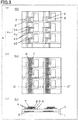
- FIG.1 An example of a thin film transistor array formed substrate 50 according to the first embodiment of the present invention is shown in Fig.1 .
- Fig.1 (a) and (b) are plan view schematically showing an example pf the thin film transistor array formed substrate 50 of the present invention.
- Fig.1 (c) is a cross-sectional view sectioned across the line B-B' of Fig.1 (b) .
- the gate wiring 2' also serves as the gate electrode 2
- the source wiring 4 also serves as the source electrode 4 having notch portions which are formed periodically, the source wiring 4 intersects the gate wiring 2', and the notch portions of the source wiring 4 are formed at portions overlapping the gate electrode 2.
- the source wiring 4 is composed of a source wiring 41 which is formed of the notch portions, having a small width, and a source wiring 42 located at a portion where no notch portion is formed, having a large width. According to the present embodiment, the source wiring 4 has an opening 4a in the source wiring 42 having a large width.
- the source wiring 4 and the drain electrode 5 are formed to form slit portions at regular intervals as the channel portions of the thin film transistors, such that the drain electrode 5 is formed, facing to each other, in the notch portion of the source wiring 4 also serving as the source electrode.
- a pixel electrode 9 is connected to the drain electrode 5. Note that the notch portions of the source wiring 4 serving as the source electrode are formed corresponding to periodical arrangement of the thin film transistor array arranged in a matrix.
- the semiconductor layer 6 is formed in a stripe shape having the longitudinal side extending in a direction where the source wiring 4 extends, and formed across the source wiring 4 and the drain electrode 5.
- the semiconductor layer 6 does not cover at least a portion in the drain electrode 5 side between both ends of the opening 4a in the width direction of the wide source wiring 42 (direction orthogonally to the direction where the source wiring 4 extends), forming a portion between the semiconductor layer 6 and the source wiring 4, in which the gate insulation layer 3, as an under layer, is exposed.
- the protection layer 7 is formed to cover the entire portion of the semiconductor layer 6 and the opening 4a. Also, the protection layer 7 is not formed on the source wiring 4 in the drain electrode 5 side, and is formed on the source wiring 4 located in a side opposite to the drain electrode 5 than to the opening 4a.
- Fig.1 (c) The cross-sectional view sectioned across the line B-B' of Fig.1 (b) is shown in Fig.1 (c) .
- the gate electrode 2 and the gate wiring 2' are formed on the substrate 1, which is covered with the gate insulation layer 3.
- the source wiring 4 and the drain electrode 5 are formed thereon.
- the semiconductor layer 6 is formed at the channel portion between the source wiring 4 and the drain electrode 5.
- the protection layer 7 is formed so as to cover the source wiring 4 also serving as the source electrode, a part of the drain electrode 5 and the semiconductor layer 6.
- the surface of the gate insulation layer 3 has ink affinity properties, and the surfaces of the source wiring 4, the drain electrode 5 and the pixel electrode 9 have ink repellent properties. Since the ink used for printing the semiconductor layer 6 is liquid, but has properties being unlikely to be influenced by the coating properties on the surface to be printed, the semiconductor layer 6 can be printed in a stripe shape as expected. In this case, it is preferable that the semiconductor layer 6 does not cover a drain side of portion of the opening 4a.
- the ink used for printing the protection layer 7 is liquid, and the ink affinity portion of the surface to be printed is likely to be wet. Hence, even the ink repellent portion is unlikely to be wet, because of the opening 4a included in the source wiring 4, the ink of the protection layer 7 tends to remain in the source wiring 4, thereby preventing the ink from leaking onto the gate insulation layer 3.
- the thin film transistor array formed substrate 50 can be manufactured by performing processes in the order of a process of forming the gate electrode 2 on the substrate 1, a process of forming the gate insulation layer 3 on the substrate 1 including the gate electrode 2, a process of simultaneously forming the source wiring 4/source electrode, the drain electrode 5 and the pixel electrode 9, a process of forming the semiconductor layer 6, and a process of forming the protection layer 7.
- the material used for the substrate 1 according to the embodiment of the present invention is not specifically limited.
- Material generally used include flexible plastic materials such as polyethylene terephthalate (PET), polyimide, polyether sulfone (PES), polyethylene naphthalate (PEN) and polycarbonate, a glass substrate such as quartz, and a silicon wafer.
- PET polyethylene terephthalate
- PES polyether sulfone
- PEN polyethylene naphthalate
- polycarbonate a glass substrate such as quartz
- silicon wafer a glass substrate
- PEN or polyimide is preferably used as the substrate.
- the electrode materials used for the gate electrode 2, the gate wiring 2', the source wiring 4, the drain electrode 5 and the pixel electrode 9 are not limited.
- a generally used material may be a thin film made of a metal or metal oxide such as gold, platinum, nickel, indium and indium tin oxide; or may be a solution in which a conductive polymer such as poly (ethylenedioxythiophene)/ polystyrene sulfonate (PEDOT/ PSS) and polyaniline, or metal colloidal particles such as gold, silver and nickel are dispersed, or may be a thick film paste using metal particles such as silver as a conductive material.
- a method for forming the gate electrode 2, the gate wiring 2', the source wiring 4, the drain electrode 5 and the pixel electrode 9 may include an ink jet method, flexographic printing, screen printing, a dispenser and offset printing.
- a material used for the gate insulation layer 3 is not specifically limited.
- Generally used materials include a polymer solution such as polyvinyl phenol, polymethylmethacrylate, polyimide, polyvinylalcohol, and a solution in which particles such as alumina or silica gel are dispersed.
- materials used for a semiconductor material of the semiconductor layer 6 are not specifically limited. Generally used materials may include polythiophene, polyallylamine, fluorenebithiophene-copolymer and polymer-based organic semiconductor materials which are similar to these derivatives, or pentacene, tetracene, copper phthalocyanine, perylene and low-molecule-based organic semiconductor material which are similar to these derivatives.
- an organic semiconductor material to which a printing method can be applied.
- Methods of forming the semiconductor layer 6 include an ink jet method, flexographic printing, screen printing, and a dispenser or the like.
- the material used for the protection layer 7 is not specifically limited. As a generally used material, fluorine based resin or polyvinylalcohol can be used, however, it is not limited to these materials.
- fluorine based resin or polyvinylalcohol can be used, however, it is not limited to these materials.
- light shielding properties can be applied as needed.
- a method of forming the protection layer 7 includes an ink jet method, flexographic printing, screen printing, and a dispenser or the like.
- Fig.2 (a) and (b) are plan views schematically showing an example of a thin film transistor array formed substrate 50 of the present invention, in which Fig.2 (c) is a cross-sectional view sectioned across the line C-C' of Fig.2(b) .
- the gate wiring 2' also serves as the gate electrode 2
- the source wiring 4 also serves as the source electrode having notch portions which are formed periodically
- the source wiring 4 intersects the gate wiring 2'
- the notch portions of the source wiring 4 are formed at portions overlapping the gate electrode 2.
- the source wiring 4 is composed of a source wiring 41 which is formed of the notch portions, having a small width, and a source wiring 42 having a large width and no notch portions.
- the source wiring 4 has an opening 4a in the source wiring 42 having a large width and no notch portions, and has an opening 4b in the source wiring 41 having a small width and the notch portions.
- the drain electrode 5 is formed in the notch portion of the source wiring 4, which faces the source wiring 4.
- the pixel electrode 9 is connected to the drain electrode 5.
- the semiconductor layer 6 is formed in a stripe shape having the longitudinal side extending in a direction where the source wiring 4 extends, and formed across the source wiring 4 and the drain electrode 5.
- the semiconductor layer 6 covers neither ends of the opening 4a in the width direction.
- the width direction refers to a line width in a direction perpendicular to a direction where the source wiring 4 extends. Accordingly, a state where the both ends in the width direction are not covered refers to a state where the width of the semiconductor layer 6 shows narrow than that of the opening 4a. Therefore, a portion is formed between the semiconductor layer 6 and the source wiring 4 which also serves as a source electrode, where the gate insulation layer 3, as an under layer, is exposed.
- the protection layer 7 covers all of the semiconductor layer 6, the opening 4a and the opening 4b, and the protection layer 7 is not formed on the both ends of the opening 4a in the width direction and on a portion of the source wiring 4 located at a side of the opening 4b opposite to the drain electrode 5.
- FIG. 2(c) A cross-sectional view sectioned across the line C-C' of Fig. 2(b) is shown in Fig.2 (c) .
- the gate wiring 2 is formed on the substrate 1, which is covered by the gate insulation layer 3.
- the source wiring 4 having openings at a part thereof and the drain electrode 5 are formed on the gate insulation layer 3.
- the semiconductor layer 6 is formed at a channel portion between the source wiring 4 and the drain electrode 5.
- the protection layer 7 is formed so as to cover the source wiring 4 in the drain electrode 5 side than to the opening, a part of the drain electrode 5 and the semiconductor layer 6.
- the surface of the gate insulation layer 3 has ink affinity properties, and the surfaces of the source wiring 4, the drain electrode 5 and the pixel electrode 9 have ink repellent properties.
- the semiconductor layer 6 can be printed in a stripe shape. In this case, preferably, the both ends of the opening 4a and one side of the opening 4b located opposite to the drain electrode 5 are not covered by the semiconductor.
- the ink used for printing the protection layer 7 is liquid, and the ink affinity portion of the surface to be printed is likely to be wet. Hence, even the ink repellent portion is unlikely to be wet, because of the openings 4a and 4b included in the source wiring 4, the ink of the protection layer 7 tends to remain in the source wiring 4, thereby preventing the ink from leaking onto the gate insulation layer 3.
- the used material and the method are the same as that of the first embodiment.
- Fig.3 (a) and (b) are plan views schematically showing an example of a thin film transistor array formed substrate 50 of the present invention, in which Fig.3 (c) is a cross-sectional view sectioned across the line D-D' of Fig.3 (b) .
- the gate electrode 2 is connected to the gate wiring 2', and the source wiring 4 also serves as the source electrode 4 having notch portions, the source wiring 4 intersects the gate wiring 2', and the notch portions of the source wiring 4 are formed on the gate electrode 2.
- the source wiring 4 is formed of a small width portion formed of the notch portions, and a large width portion where no notch portion is formed.
- the opening 4a formed in the source wiring 42 having a large width shown in Fig.3 (a) , and an opening 4b formed in the source wiring 41 are connected to form an opening 4c communicated therebetween.
- the source wiring 4 shows a wiring constituted of a linear part and a rectangular-wave like part. Note that both parts are electrically connected.
- the drain electrode 5 is formed in the notch portion of the source wiring 4, facing the source wiring 4.
- the pixel electrode 9 is connected to the drain electrode 5.
- the semiconductor layer 6 is formed in a direction where the source wiring 4 extends, and formed across the source wiring 4 and the drain electrode 5.
- the semiconductor layer 6 is formed in a stripe shape extending in parallel to the source wiring 4, excluding a source wiring at the both ends in a width direction (perpendicular to a direction where the source wiring extends) of the opening 4c.
- the protection layer 7 covers all of the semiconductor layer 6 and the opening 4c through which the source wiring 41 having small width and the source wiring 42 having large width are communicated.
- the protection layer 7 is not formed on the source wiring 4 at both ends side of the opening 4c in the width direction.
- FIG.3 (c) A cross-sectional view sectioned across the line D-D' of Fig. 3 (b) is shown in Fig.3 (c) .
- the gate electrode 2, the gate wiring 2' are formed on the substrate 1, which is covered by the gate insulation layer 3.
- the source wiring 4 having openings at a part thereof and the drain electrode 5 are formed on the gate insulation layer 3.
- the semiconductor layer 6 is formed at a channel portion between the source wiring 4 and the drain electrode 5.
- the protection layer 7 is formed so as to cover the source wiring 4 on the drain electrode 5 side than to the opening, a part of the drain electrode 5 and the semiconductor layer 6.
- the surface of the gate insulation layer 3 shows ink affinity properties
- the surfaces of the source wiring 4, the drain electrode 5 and the pixel electrode 9 show ink repellent properties.
- the semiconductor layer 6 can be printed in a long stripe shape as expected.
- the semiconductor layer 6 does not cover a part of the source wiring having a large width, located at both ends of the opening 4a in the opening 4c, and a part of the source wiring having a small width, located at opposite side to the drain electrode 5 with respect to the opening 4b.
- the ink used for printing the protection layer 7 is liquid, and the ink affinity portion of the surface to be printed is likely to be wet.
- the ink repellent portion is unlikely to be wet, because of the opening 4c included in the source wiring 4, the ink of the protection layer 7 tends to remain in the opening 4c in the source wiring 4, thereby preventing the ink from leaking onto the gate insulation layer 3.
- the used material and the method are the same as that of the first embodiment.
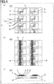
- Fig.4 (a) and (b) are plan views schematically showing an example of a thin film transistor array formed substrate 50 of the present invention, in which Fig.4 (c) is a cross-sectional view sectioned across the line E-E' of Fig.4 (b) .
- the gate electrode 2 is connected to the gate wiring 2', and the source wiring 4 also serves as the source electrode 4 having notch portions, the source wiring 4 intersects the gate wiring 2', and the notch portions of the source wiring 4 are formed on the gate electrode 2.
- the source wiring 4 is formed of a small width portion formed of the notch portions, and a large width portion where no notch portion is formed.
- the opening 4a formed in the source wiring 42 having a large width, and an opening 4b formed in the source wiring 41 shown in Fig.4 (a) are partly connected to form an opening 4d communicated therebetween.
- the source wiring 4 has a wiring constituted of a linear part and a rectangular-wave like part. Note that both parts are electrically connected.
- opening 4d communicated therebetween may be partly connected between a plurality of openings 4a and 4b.
- the drain electrode 5 is formed in the notch portion of the source wiring 4, facing the source wiring 4.
- the pixel electrode 9 is connected to the drain electrode 5.
- the semiconductor layer 6 is formed in a direction where the source wiring 4 extends, and formed across the source wiring 4 and the drain electrode 5.
- the semiconductor layer 6 is formed in a stripe shape extending parallel to the source wiring 4, excluding a source wiring at the both ends in a width direction (perpendicular to a direction where the source wiring extends) of the opening 4d.
- the protection layer 7 covers all of the semiconductor layer 6 and the openings 4d through which the source wiring 42 having large width and the source wiring 41 having small width are partly communicated.
- the protection layer 7 is not formed on the source wiring 4 at both ends side of the opening 4d in the width direction.
- FIG. 4 (c) A cross-sectional view sectioned across the line E-E' of Fig. 4 (b) is shown in Fig.4 (c) .
- the gate electrode 2 the gate wiring 2' is formed on the substrate 1, which is covered by the gate insulation layer 3.
- the source wiring 4 having openings at a part thereof and the drain electrode 5 are formed on the gate insulation layer 3.
- the semiconductor layer 6 is formed at a channel portion between the source wiring 4 and the drain electrode 5.
- the protection layer 7 is formed so as to cover the source wiring 4 in the drain electrode 5 side than to the opening, a part of the drain electrode 5 and the semiconductor layer 6.
- the surface of the gate insulation layer 3 has ink affinity properties, and the surfaces of the source wiring 4, the drain electrode 5 and the pixel electrode 9 have ink repellent properties.
- the semiconductor layer 6 can be printed in a long stripe shape as expected.
- the semiconductor layer 6 does not cover a part of the source wiring having a large width, located at the both ends of the opening 4a in the opening 4d, and a part of the source wiring 4 having a small width, located at opposite side to the drain electrode 5 with respect to the opening 4b.
- the ink used for printing the protection layer 7 is liquid, and the ink affinity portion of the surface to be printed is likely to be wet.
- the ink repellent portion is unlikely to be wet, because of the opening 4d included in the source wiring 4, the ink of the protection layer 7 tends to remain in the opening 4d in the source wiring 4, thereby preventing the ink from leaking onto the gate insulation layer 3.
- the material and the method are the same as that of the first embodiment.
- a capacitor electrode and a capacitor wiring which are not shown may be arranged in the same layer as the gate electrode 2 and the gate wiring 2'.
- the capacitor electrode becomes a storage capacitor when overlapped with the pixel electrode 9 via the gate insulation layer 3.
- the storage capacitor maintains the voltage of the pixel electrode.
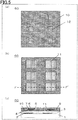
- the fifth embodiment of the present invention is an image display device substrate 60 provided with a thin film transistor array formed substrate 50.
- the image display device substrate 60 as the fifth embodiment of the present invention is provided with, as shown in Fig.5 (c) , an interlayer insulation layer 10 formed on the thin film transistor array formed substrate 50 according to any one of the first to fourth embodiments of the present invention. Further, the image display device substrate 60 includes an opening 12 in the interlayer insulation layer 10 formed on the pixel electrode 9. In this case, the opening 12 of the interlayer insulation layer 10 serves as an effective pixel region. Alternatively, an upper pixel electrode 11 is further formed on the interlayer insulation layer 10 and the upper electrode 11 is connected to the pixel electrode 9, whereby the upper pixel electrode 11 serves as an effective pixel region.
- Fig.5 (a) is an overall plan view showing an example of a state where the interlayer insulation layer 10 is formed on the thin film transistor array formed substrate 50 of the present invention, including openings at required portions.
- Fig.5 (b) is an example of a brief plan view showing an example of a state where the upper pixel electrode 11 is formed on the configuration shown in Fig.5 (a).
- Fig.5(c) illustrates a state where the upper pixel electrode 11 is connected to the pixel electrode 9 via the opening 12 of the interlayer insulation layer 10.
- interlayer insulation layer 10 As a material of the interlayer insulation layer 10, polyvinyl phenol, acryl, epoxy, polyimide or the like can be used. As a method for forming the interlayer insulation layer 10, screen printing is preferably used. However, a photosensitive interlayer insulation layer may be formed, and then exposed/developed, thereby forming the interlayer insulation layer 10.
- metal such as Al, Cr, Au, Ag, Ni and Cu, or a transparent conductive layer such as ITO can be used.
- a method for forming the upper pixel electrode 11 it is possible to apply photolithography or etching after performing a film-formation using deposition or sputtering. However, screen printing is preferably applied using Ag ink, Ni ink, Cu ink or the like.
- the inventors prepared a substrate 1 on which the gate wiring 2' and the gate insulation layer 3 are formed shown in Fig.1 , and formed the source wiring 4 and the drain electrode 5 by using a printing method.
- the semiconductor layer 6 was formed over a plurality of transistors, by using a coating method, in a region of the source wiring 4 including notch portions such that the semiconductor layer 6 was formed in a long stripe shape not to coat the entire opening 4a of the source wiring having a large width, but to expose a part of the opening 4a.
- the protection layer 7 was formed over the plurality of transistors in a long stripe shape, by using a coating method, to cover the entire semiconductor layer 6 and the openings 4a of the source wiring having a large width and the source wiring 4 in a side opposite to the drain electrode 5.
- PEN polyethylene naphthalate
- nanosilver ink is used in which the weight ratio between nanosilver and polyethylene glycol#200 is 8:1.
- the nanosilver ink is printed on a PEN substrate 1 by transfer printing, followed by a baking at 180 °C for one hour to form the gate wiring 2'.
- a solution was used in which polyvinyl phenol was dissolved into cyclohexanone at 10 weight %.
- a solution of the gate insulation layer 3 is coated by a die coater method, followed by a drying at 180°C at one hour.
- the contact angle of the water of the gate insulation layer 3 was 75° or less.
- nanosilver ink is used in which the weight ratio between nanosilver and polyethylene glycol#200 is 8:1.
- the nanosilver ink is printed by transfer printing, followed by drying at 180°C for one hour to form the source wiring 4 and the drain electrode 5.
- the contact angle of the water of the source wiring 4 and the drain electrode was 80° or more.
- the semiconductor layer 6 a solution was used in which fluorene-bithiophene copolymer (F8T2) was dissolved into tetralin at 1.0 weight %.
- F8T2 fluorene-bithiophene copolymer
- the semiconductor layer 8 was formed over the plurality of transistors using a coating method such that the semiconductor layer 6 was coated on the region of the source wiring 4 having notch portions, followed by the drying at 100°C for one hour.
- an ink was used in which polyvinyl alcohol was dissolved into the pure water at 5 weight % to form the protection layer 7 right above the semiconductor layer 6.
- the inventors prepared a substrate shown in Fig.2 on which the gate wiring and the gate insulation layer were formed, and formed the source wiring and the drain electrode by using a printing method. An etching was performed to form the opening 4a in the source wiring having a large width and the opening 4b in the source wiring having a small width.
- the semiconductor layer 6 was formed over the plurality of transistors, by using a coating method, in a long stripe shape not to coat the entire opening of the source wiring having a large width, but to allow a part of the opening 4a to remain exposed.
- the protection layer 7 was formed over the plurality of transistors in a long stripe shape, by using a coating method, to cover the entire semiconductor layer and the openings 4a of the source wiring having a large width and the source wiring 4 in a side opposite to the drain electrode 5.
- the method for forming the source wiring 4 and the drain electrode 5 except pattern of the printing plate and the material thereof are the same as that of the example 1.
- the openings were formed in the source wiring having a large width.
- the openings are provided in a source wiring having concave-convex portion, that is a source wiring part having a large width and a source wiring part having a small width, whereby a desired pattern of the protection layer was able to be formed regardless of a wettability of the surface to be printed.
- the source wiring 4 and the drain electrode 5 are formed on the substrate 1 on which the gate wiring 2' and the gate insulation layer 3 are formed.
- the semiconductor layer 6 is formed in a long stripe shape over the plurality of transistors.
- the protection layer 7 was formed so as to coat the entire semiconductor 6 over the plurality of transistors.
- the pattern of the protection layer was influenced by the wettability of the surface to be printed so that a desired long stripe pattern could not be formed. Hence, the entire semiconductor layer was not be able to be coated.
- the source wiring has periodic notch patterns in the width direction, and the openings are formed in the source wiring, whereby leakage is avoided when the protection layer is formed and desired protection layer pattern can be formed.
Landscapes
- Engineering & Computer Science (AREA)
- Manufacturing & Machinery (AREA)
- Microelectronics & Electronic Packaging (AREA)
- Thin Film Transistor (AREA)
Abstract
a pixel electrode connected to the drain electrode; a semiconductor layer; and a protection layer, which are laminated in this order, in which the source wiring serving as both the source wiring and the source electrode has notch portions periodically formed in a direction where the source wiring extends; the notch portions of the source wiring are formed at portions overlapping the gate electrode; portions where the notch portions exist correspond to a source wiring having a small width, and portions where no notch portions correspond to a source wiring having a large width which is wider than the source wiring having the small width; the source wiring having the large width at least includes an opening; the semiconductor layer is formed in a stripe shape having a longitudinal side extending in a direction where the source wiring extends, and formed across the source electrode and the drain electrode; and the protection layer is formed to cover entire portion of the semiconductor layer.
Description
- The present invention relates to a substrate for forming a thin film transistor array, an image display device substrate and a manufacturing method of a substrate for forming a thin film transistor array.
- To form patterns of a semiconductor layer and a protection layer in the thin film transistors, a method is utilized in which each of the semiconductor layer and the protection layer are formed on the entire surface, resist patterns are formed, and etching is applied to the resist patterns using etchant so as to form the patterns. However, with this method, the resist has to be film-formed followed by the etching for every time when forming respective patterns. As a result, the number of manufacturing steps increases.
- As an example, according to
PTL 1, thickness of the resist is adjusted to form the pattern by using only one photolithography process. However, the photolithography process cannot be omitted. - On the other hand, when using a printing technique to form the semiconductor layer and the protection layer, especially when liquid is used for the material of the semiconductor layer and the protection layer, desired pattern may not be formed.
-
Fig.6 (a) and (b) are plan views schematically showing an example of a conventional thin film transistor array formedsubstrate 50, andFig.6 (c) shows a cross-sectional view sectioned across A-A' line ofFig.6 (b) . - As shown in
Fig.6 (a) , when viewing a layout as a planar arrangement, thegate electrode 2 is connected to the gate wiring 2', the source wiring 4 also serves as the source electrode, the source wiring 4 has periodic notch portions, the source wiring 4 intersects the gate wiring 2', and the notch portions of the source wiring 4 are formed on thegate electrode 2.Drain electrodes 5 are formed in the notch portions of the source wiring 4, facing the source wiring 4. - In the case where the
semiconductor layer 6 is formed on the thin film transistor array formedsubstrate 50 which is formed in this manner, and theprotection layer 7 is formed in a stripe pattern, as shown inFig.6 (b) , thesemiconductor layer 6 can be formed to connect the source wiring 4 and thedrain electrode 5, however, theprotection layer 7 may be formed to cover a part of thesemiconductor layer 6, the source wiring 4 and thegate insulation layer 3, excluding a part ofsemiconductor layer 6 in thedrain electrode 5 side and a part of the source wiring 4. In other words, a part of thesemiconductor layer 6 may not be covered by theprotection layer 7. - As shown in
Fig.6 (c) , where the cross-sectional view across the line A-A' shown inFig.6 (b) is illustrated, thegate electrode 2 and the gate wiring 2' are formed on thesubstrate 1, which are covered by thegate insulation layer 3, and further the source wiring 4 and thedrain electrode 5 are formed thereon. Thesemiconductor layer 6 is formed at a channel portion between the source wiring 4 and thedrain electrode 5, and theprotection layer 7 is formed to cover the source wiring 4 and thesemiconductor layer 6, excluding a part of thesemiconductor layer 6 on thedrain electrode 5 side. - Thus, according to the conventional structure, the shape of the
protection layer 7 is sometimes worsened. The inventors have found out the cause of this problem is that liquid state ink on the wiring flows onto thegate insulation layer 3. - In
Fig.6 (a) , the surface of thegate insulation layer 3 has ink affinity properties, and the surfaces of the source wiring 4, thedrain electrode 5 and thepixel electrode 9 have ink repellent properties. Since the ink used for printing thesemiconductor layer 6 is liquid, but has properties being unlikely to be influenced by the wettability of the surface to be printed, thesemiconductor layer 6 can be printed in a stripe shape as expected. On the other hand, an ink used for printing theprotection layer 7 is also a liquid. However, an ink affinity portion of the surface to be printed is likely to be wet and an ink repellent portion is unlikely to be wet, whereby the ink on the source wiring 4 and thedrain electrode 5 is repelled to move onto thegate insulation layer 3, producing an irregular shape shown inFig.6 (b) and (c) . This is what the inventors have discovered. - [PTL 1] International Publication Number
2012/172985 . - When pattering the protection layer, generally, a photolithography process is used for the pattering. However, photolithography process requires a large number of manufacturing processes, and has disadvantages that high cost is required for equipment and materials for the patterning.
- In contrast, according to a printing method, by using a printing plate, it is possible to form the protection layer pattern without increasing the number of manufacturing processes. However, when the surface to be printed is composed of a plurality of materials, there is a concern that the printed pattern may be different from the designed pattern. For example, when the printed semiconductor layer connects between the source and the drain on a portion where the gate electrode is not formed, off current increases. Also, when the protection layer is not able to cover the semiconductor layer completely, the semiconductor cannot be prevented from being degraded.
- The present invention is achieved in light of the above-described problems, and has an object to provide a substrate for forming a thin film transistor array capable of performing patterning favorable for the semiconductor layer and the protection layer, a manufacturing method thereof, and an image display device substrate using the substrate for forming the thin film transistor array.
- A first aspect of the present invention as a means for solving the above-described problems is a thin film transistor array substrate prepared including a gate electrode; a gate insulation layer; a source electrode; a drain electrode; a pixel electrode connected to the drain electrode; a semiconductor layer; and a protection layer, which are laminated in this order. A source wiring serving as both the source wiring and the source electrode has notch portions periodically formed in a direction where the source wiring extends; the notch portions of the source wiring are formed at portions overlapping the gate electrode; portions where the notch portions exist correspond to a source wiring having a small width, and portions where no notch portions exist correspond to a source wiring having a large width which is wider than the source wiring having the small width; the source wiring having the large width at least includes an opening; the semiconductor layer is formed in a stripe shape having a longitudinal side extending in a direction where the source wiring extends, and formed across the source electrode and the drain electrode; and the protection layer is formed to cover an entire portion of the semiconductor layer.
- The source wiring having a small width may include another opening.
- The opening of the source wiring having the small width and the opening of the source wiring having the large width may be communicated in a direction where the source wiring extends.
- The opening of the source wiring having the small width and the opening of the source wiring having the large width may form an opening in a direction where the source wiring extends, the opening partly communicating therethrough.
- Other aspect of the present invention is an image display device substrate provided with an interlayer insulation layer on the above-described thin film transistor array formed substrate, having an opening in the interlayer insulation layer at a portion corresponding to the pixel electrode in the interlayer insulation layer.
- An upper pixel electrode may be further provided on the interlayer insulation film, and the upper pixel electrode may be connected to the pixel electrode of the thin film transistor array formed substrate via the opening of the interlayer insulation layer.
- Other aspect of the present invention is a manufacturing method of forming the above-described thin film transistor array substrate including processes performed in the order of: a process of forming a gate electrode on a substrate; a process of forming a gate insulation layer on the substrate including the gate electrode; a process of simultaneously forming a source wiring serving as both the source wiring and a source electrode, a drain electrode and a pixel electrode; a process of forming a semiconductor layer by a printing method using liquid state ink; and a process of forming a protection layer by a printing method using the liquid state ink.
- Offset printing may be used for forming the source wiring serving as both the source wiring and the source electrode, the drain electrode and the pixel electrode, in the process of simultaneously forming a source wiring serving as both the source wiring and a source electrode, a drain electrode and a pixel electrode.
- The semiconductor layer may be formed to cover neither both ends in a width direction of the opening of the source wiring, in the process of forming the semiconductor layer.
- The protection layer may be formed to cover all of the semiconductor layer and the opening of the source wiring, in the process of forming the protection layer.
- According to the present invention, without increasing the number of manufacturing processes, a substrate for forming a thin film transistor array capable of performing favorable patterning of a semiconductor layer and a protection layer, a manufacturing method thereof, and an image display device substrate using the substrate for the thin film transistor array can be provided.
-
-
Fig. 1 is a set of diagrams in which (a) is a plan view schematically showing an example of a substrate for forming a thin film transistor array during a manufacturing process according to the present invention, and (b) and (c) are a plan view and a cross-sectional view respectively, schematically showing an example of the substrate for forming the thin film transistor array according to the present invention. -
Fig.2 is a set of diagrams in which (a) is a plan view schematically showing an example of a substrate for forming a thin film transistor array during a manufacturing process according to the present invention, and (b) and (c) are a plan view and a cross-sectional view respectively, schematically showing an example of the substrate for forming the thin film transistor array according to the present invention. -
Fig.3 is a set of diagrams in which (a) is a plan view schematically showing an example of a substrate for forming a thin film transistor array during a manufacturing process according to the present invention, and (b) and (c) are a plan view and a cross-sectional view respectively, schematically showing an example of the substrate for forming the thin film transistor array according to the present invention. -
Fig.4 is a set of diagrams in which (a) is a plan view schematically showing an example of a substrate for forming a thin film transistor array during a manufacturing process according to the present invention, and (b) and (c) are a plan view and a cross-sectional view respectively, schematically showing an example of the substrate for forming the thin film transistor array according to the present invention. -
Fig.5 is a set of diagrams including plan views and a cross-sectional view each schematically showing an example of a substrate for forming a thin film transistor array during a manufacturing process according to the present invention, in which (a) shows an interlayer insulation later and openings of the interlayer insulation layer formed therein, (b) shows upper pixel electrodes formed on the interlayer insulation layer, and (c) shows a cross-sectional view sectioned across line F-F' of (b). -
Fig.6 is a set of diagrams in which (a) is a plan view schematically showing an example of a substrate for forming a thin film transistor array during a manufacturing process according to a conventional art, and (b) and (c) are a plan view and a cross-sectional view respectively, schematically showing an example of the substrate for forming the thin film transistor array according to a conventional art. - With reference to the drawings, hereinafter, embodiments of the present invention will be described in detail.
- With reference to
Fig.1 , a first embodiment of the present invention will be described. - An example of a thin film transistor array formed
substrate 50 according to the first embodiment of the present invention is shown inFig.1 . -
Fig.1 (a) and (b) are plan view schematically showing an example pf the thin film transistor array formedsubstrate 50 of the present invention.Fig.1 (c) is a cross-sectional view sectioned across the line B-B' ofFig.1 (b) . As shown inFig.1 (a) , when viewing a layout as a planar arrangement, the gate wiring 2' also serves as thegate electrode 2, and the source wiring 4 also serves as the source electrode 4 having notch portions which are formed periodically, the source wiring 4 intersects the gate wiring 2', and the notch portions of the source wiring 4 are formed at portions overlapping thegate electrode 2. The source wiring 4 is composed of asource wiring 41 which is formed of the notch portions, having a small width, and asource wiring 42 located at a portion where no notch portion is formed, having a large width. According to the present embodiment, the source wiring 4 has an opening 4a in thesource wiring 42 having a large width. The source wiring 4 and thedrain electrode 5 are formed to form slit portions at regular intervals as the channel portions of the thin film transistors, such that thedrain electrode 5 is formed, facing to each other, in the notch portion of the source wiring 4 also serving as the source electrode. Apixel electrode 9 is connected to thedrain electrode 5. Note that the notch portions of the source wiring 4 serving as the source electrode are formed corresponding to periodical arrangement of the thin film transistor array arranged in a matrix. - As shown in
Fig. 1 (b) , thesemiconductor layer 6 is formed in a stripe shape having the longitudinal side extending in a direction where the source wiring 4 extends, and formed across the source wiring 4 and thedrain electrode 5. Thesemiconductor layer 6 does not cover at least a portion in thedrain electrode 5 side between both ends of theopening 4a in the width direction of the wide source wiring 42 (direction orthogonally to the direction where the source wiring 4 extends), forming a portion between thesemiconductor layer 6 and the source wiring 4, in which thegate insulation layer 3, as an under layer, is exposed. Theprotection layer 7 is formed to cover the entire portion of thesemiconductor layer 6 and theopening 4a. Also, theprotection layer 7 is not formed on the source wiring 4 in thedrain electrode 5 side, and is formed on the source wiring 4 located in a side opposite to thedrain electrode 5 than to theopening 4a. - The cross-sectional view sectioned across the line B-B' of
Fig.1 (b) is shown inFig.1 (c) . As shown inFig.1 (c) , thegate electrode 2 and the gate wiring 2' are formed on thesubstrate 1, which is covered with thegate insulation layer 3. Further, the source wiring 4 and thedrain electrode 5 are formed thereon. Thesemiconductor layer 6 is formed at the channel portion between the source wiring 4 and thedrain electrode 5. Theprotection layer 7 is formed so as to cover the source wiring 4 also serving as the source electrode, a part of thedrain electrode 5 and thesemiconductor layer 6. - In
Fig. 1 (a) , the surface of thegate insulation layer 3 has ink affinity properties, and the surfaces of the source wiring 4, thedrain electrode 5 and thepixel electrode 9 have ink repellent properties. Since the ink used for printing thesemiconductor layer 6 is liquid, but has properties being unlikely to be influenced by the coating properties on the surface to be printed, thesemiconductor layer 6 can be printed in a stripe shape as expected. In this case, it is preferable that thesemiconductor layer 6 does not cover a drain side of portion of theopening 4a. The ink used for printing theprotection layer 7 is liquid, and the ink affinity portion of the surface to be printed is likely to be wet. Hence, even the ink repellent portion is unlikely to be wet, because of theopening 4a included in the source wiring 4, the ink of theprotection layer 7 tends to remain in the source wiring 4, thereby preventing the ink from leaking onto thegate insulation layer 3. - The thin film transistor array formed
substrate 50 can be manufactured by performing processes in the order of a process of forming thegate electrode 2 on thesubstrate 1, a process of forming thegate insulation layer 3 on thesubstrate 1 including thegate electrode 2, a process of simultaneously forming the source wiring 4/source electrode, thedrain electrode 5 and thepixel electrode 9, a process of forming thesemiconductor layer 6, and a process of forming theprotection layer 7. - The material used for the
substrate 1 according to the embodiment of the present invention is not specifically limited. Material generally used include flexible plastic materials such as polyethylene terephthalate (PET), polyimide, polyether sulfone (PES), polyethylene naphthalate (PEN) and polycarbonate, a glass substrate such as quartz, and a silicon wafer. However, taking required flexibility and each process temperature into consideration, PEN or polyimide is preferably used as the substrate. - In the embodiments of the present invention, the electrode materials used for the
gate electrode 2, the gate wiring 2', the source wiring 4, thedrain electrode 5 and thepixel electrode 9 are not limited. However, a generally used material may be a thin film made of a metal or metal oxide such as gold, platinum, nickel, indium and indium tin oxide; or may be a solution in which a conductive polymer such as poly (ethylenedioxythiophene)/ polystyrene sulfonate (PEDOT/ PSS) and polyaniline, or metal colloidal particles such as gold, silver and nickel are dispersed, or may be a thick film paste using metal particles such as silver as a conductive material. A method for forming thegate electrode 2, the gate wiring 2', the source wiring 4, thedrain electrode 5 and thepixel electrode 9 may include an ink jet method, flexographic printing, screen printing, a dispenser and offset printing. - In the embodiments of the present invention, a material used for the
gate insulation layer 3 is not specifically limited. Generally used materials include a polymer solution such as polyvinyl phenol, polymethylmethacrylate, polyimide, polyvinylalcohol, and a solution in which particles such as alumina or silica gel are dispersed. - In the embodiments of the present invention, materials used for a semiconductor material of the
semiconductor layer 6 are not specifically limited. Generally used materials may include polythiophene, polyallylamine, fluorenebithiophene-copolymer and polymer-based organic semiconductor materials which are similar to these derivatives, or pentacene, tetracene, copper phthalocyanine, perylene and low-molecule-based organic semiconductor material which are similar to these derivatives. However, considering requirements of low cost, flexibility and large area, it is preferable to use an organic semiconductor material to which a printing method can be applied. Methods of forming thesemiconductor layer 6 include an ink jet method, flexographic printing, screen printing, and a dispenser or the like. - In the embodiments of the present invention, the material used for the
protection layer 7 is not specifically limited. As a generally used material, fluorine based resin or polyvinylalcohol can be used, however, it is not limited to these materials. For theprotection layer 7, light shielding properties can be applied as needed. A method of forming theprotection layer 7 includes an ink jet method, flexographic printing, screen printing, and a dispenser or the like. - With reference to
Fig.2 , the second embodiment of the present invention will be described. -
Fig.2 (a) and (b) are plan views schematically showing an example of a thin film transistor array formedsubstrate 50 of the present invention, in whichFig.2 (c) is a cross-sectional view sectioned across the line C-C' ofFig.2(b) . - As shown in
Fig.2 (a) , when viewing a layout as a planar arrangement, the gate wiring 2' also serves as thegate electrode 2, and the source wiring 4 also serves as the source electrode having notch portions which are formed periodically, the source wiring 4 intersects the gate wiring 2', and the notch portions of the source wiring 4 are formed at portions overlapping thegate electrode 2. The source wiring 4 is composed of asource wiring 41 which is formed of the notch portions, having a small width, and asource wiring 42 having a large width and no notch portions. According to the present embodiment, the source wiring 4 has anopening 4a in thesource wiring 42 having a large width and no notch portions, and has anopening 4b in thesource wiring 41 having a small width and the notch portions. Also, thedrain electrode 5 is formed in the notch portion of the source wiring 4, which faces the source wiring 4. Moreover, thepixel electrode 9 is connected to thedrain electrode 5. - As shown in
Fig.2 (b) , thesemiconductor layer 6 is formed in a stripe shape having the longitudinal side extending in a direction where the source wiring 4 extends, and formed across the source wiring 4 and thedrain electrode 5. Thesemiconductor layer 6 covers neither ends of theopening 4a in the width direction. Note that the width direction refers to a line width in a direction perpendicular to a direction where the source wiring 4 extends. Accordingly, a state where the both ends in the width direction are not covered refers to a state where the width of thesemiconductor layer 6 shows narrow than that of theopening 4a. Therefore, a portion is formed between thesemiconductor layer 6 and the source wiring 4 which also serves as a source electrode, where thegate insulation layer 3, as an under layer, is exposed. On the other hand, theprotection layer 7 covers all of thesemiconductor layer 6, theopening 4a and theopening 4b, and theprotection layer 7 is not formed on the both ends of theopening 4a in the width direction and on a portion of the source wiring 4 located at a side of theopening 4b opposite to thedrain electrode 5. - A cross-sectional view sectioned across the line C-C' of
Fig. 2(b) is shown inFig.2 (c) . As shown inFig. 2(c) , thegate wiring 2 is formed on thesubstrate 1, which is covered by thegate insulation layer 3. Further, the source wiring 4 having openings at a part thereof and thedrain electrode 5 are formed on thegate insulation layer 3. Thesemiconductor layer 6 is formed at a channel portion between the source wiring 4 and thedrain electrode 5. Theprotection layer 7 is formed so as to cover the source wiring 4 in thedrain electrode 5 side than to the opening, a part of thedrain electrode 5 and thesemiconductor layer 6. - In
Fig.2 (a) , the surface of thegate insulation layer 3 has ink affinity properties, and the surfaces of the source wiring 4, thedrain electrode 5 and thepixel electrode 9 have ink repellent properties. - Since the ink used for printing the
semiconductor layer 6 is liquid, but has properties being unlikely to be influenced by the coating properties on the surface to be printed, thesemiconductor layer 6 can be printed in a stripe shape. In this case, preferably, the both ends of theopening 4a and one side of theopening 4b located opposite to thedrain electrode 5 are not covered by the semiconductor. - The ink used for printing the
protection layer 7 is liquid, and the ink affinity portion of the surface to be printed is likely to be wet. Hence, even the ink repellent portion is unlikely to be wet, because of theopenings protection layer 7 tends to remain in the source wiring 4, thereby preventing the ink from leaking onto thegate insulation layer 3. - The used material and the method are the same as that of the first embodiment.
- With reference to
Fig.3 , the third embodiment of the present invention will be described. -
Fig.3 (a) and (b) are plan views schematically showing an example of a thin film transistor array formedsubstrate 50 of the present invention, in whichFig.3 (c) is a cross-sectional view sectioned across the line D-D' ofFig.3 (b) . As shown inFig.3 (a) , when viewing a layout as a planar arrangement, thegate electrode 2 is connected to the gate wiring 2', and the source wiring 4 also serves as the source electrode 4 having notch portions, the source wiring 4 intersects the gate wiring 2', and the notch portions of the source wiring 4 are formed on thegate electrode 2. The source wiring 4 is formed of a small width portion formed of the notch portions, and a large width portion where no notch portion is formed. According to the present embodiment, theopening 4a formed in thesource wiring 42 having a large width shown inFig.3 (a) , and anopening 4b formed in thesource wiring 41 are connected to form anopening 4c communicated therebetween. As a result, the source wiring 4 shows a wiring constituted of a linear part and a rectangular-wave like part. Note that both parts are electrically connected. - Moreover, similar to the first and second embodiments, the
drain electrode 5 is formed in the notch portion of the source wiring 4, facing the source wiring 4. Thepixel electrode 9 is connected to thedrain electrode 5. As shown inFig.3 (b) , thesemiconductor layer 6 is formed in a direction where the source wiring 4 extends, and formed across the source wiring 4 and thedrain electrode 5. Thesemiconductor layer 6 is formed in a stripe shape extending in parallel to the source wiring 4, excluding a source wiring at the both ends in a width direction (perpendicular to a direction where the source wiring extends) of theopening 4c. - The
protection layer 7 covers all of thesemiconductor layer 6 and theopening 4c through which thesource wiring 41 having small width and thesource wiring 42 having large width are communicated. Theprotection layer 7 is not formed on the source wiring 4 at both ends side of theopening 4c in the width direction. - A cross-sectional view sectioned across the line D-D' of
Fig. 3 (b) is shown inFig.3 (c) . As shown inFig. 3 (c) , thegate electrode 2, the gate wiring 2' are formed on thesubstrate 1, which is covered by thegate insulation layer 3. Further, the source wiring 4 having openings at a part thereof and thedrain electrode 5 are formed on thegate insulation layer 3. Thesemiconductor layer 6 is formed at a channel portion between the source wiring 4 and thedrain electrode 5. Theprotection layer 7 is formed so as to cover the source wiring 4 on thedrain electrode 5 side than to the opening, a part of thedrain electrode 5 and thesemiconductor layer 6. - In
Fig.3 (a) , the surface of thegate insulation layer 3 shows ink affinity properties, and the surfaces of the source wiring 4, thedrain electrode 5 and thepixel electrode 9 show ink repellent properties. - Since the ink used for printing the
semiconductor layer 6 is liquid, but has properties being unlikely to be influenced by the coating properties on the surface to be printed, thesemiconductor layer 6 can be printed in a long stripe shape as expected. In this case, preferably, thesemiconductor layer 6 does not cover a part of the source wiring having a large width, located at both ends of theopening 4a in theopening 4c, and a part of the source wiring having a small width, located at opposite side to thedrain electrode 5 with respect to theopening 4b. The ink used for printing theprotection layer 7 is liquid, and the ink affinity portion of the surface to be printed is likely to be wet. Hence, even though the ink repellent portion is unlikely to be wet, because of theopening 4c included in the source wiring 4, the ink of theprotection layer 7 tends to remain in theopening 4c in the source wiring 4, thereby preventing the ink from leaking onto thegate insulation layer 3. - The used material and the method are the same as that of the first embodiment.
- With reference to
Fig.4 , the fourth embodiment of the present invention will be described. -
Fig.4 (a) and (b) are plan views schematically showing an example of a thin film transistor array formedsubstrate 50 of the present invention, in whichFig.4 (c) is a cross-sectional view sectioned across the line E-E' ofFig.4 (b) . As shown inFig.4 (a) , when viewing a layout as a planar arrangement, thegate electrode 2 is connected to the gate wiring 2', and the source wiring 4 also serves as the source electrode 4 having notch portions, the source wiring 4 intersects the gate wiring 2', and the notch portions of the source wiring 4 are formed on thegate electrode 2. The source wiring 4 is formed of a small width portion formed of the notch portions, and a large width portion where no notch portion is formed. According to the present embodiment, theopening 4a formed in thesource wiring 42 having a large width, and anopening 4b formed in thesource wiring 41 shown inFig.4 (a) are partly connected to form anopening 4d communicated therebetween. As a result, the source wiring 4 has a wiring constituted of a linear part and a rectangular-wave like part. Note that both parts are electrically connected. - Note that the
opening 4d communicated therebetween may be partly connected between a plurality ofopenings - Moreover, similar to the first, second and third embodiments, the
drain electrode 5 is formed in the notch portion of the source wiring 4, facing the source wiring 4. Thepixel electrode 9 is connected to thedrain electrode 5. As shown inFig.4 (b) , thesemiconductor layer 6 is formed in a direction where the source wiring 4 extends, and formed across the source wiring 4 and thedrain electrode 5. Thesemiconductor layer 6 is formed in a stripe shape extending parallel to the source wiring 4, excluding a source wiring at the both ends in a width direction (perpendicular to a direction where the source wiring extends) of theopening 4d. - The
protection layer 7 covers all of thesemiconductor layer 6 and theopenings 4d through which thesource wiring 42 having large width and thesource wiring 41 having small width are partly communicated. Theprotection layer 7 is not formed on the source wiring 4 at both ends side of theopening 4d in the width direction. - A cross-sectional view sectioned across the line E-E' of
Fig. 4 (b) is shown inFig.4 (c) . As shown inFig. 4 (c) , thegate electrode 2, the gate wiring 2' is formed on thesubstrate 1, which is covered by thegate insulation layer 3. Further, the source wiring 4 having openings at a part thereof and thedrain electrode 5 are formed on thegate insulation layer 3. Thesemiconductor layer 6 is formed at a channel portion between the source wiring 4 and thedrain electrode 5. Theprotection layer 7 is formed so as to cover the source wiring 4 in thedrain electrode 5 side than to the opening, a part of thedrain electrode 5 and thesemiconductor layer 6. - In
Fig.4 (a) , the surface of thegate insulation layer 3 has ink affinity properties, and the surfaces of the source wiring 4, thedrain electrode 5 and thepixel electrode 9 have ink repellent properties. - Since the ink used for printing the
semiconductor layer 6 is liquid, but has properties being unlikely to be influenced by the coating properties on the surface to be printed, thesemiconductor layer 6 can be printed in a long stripe shape as expected. In this case, preferably, thesemiconductor layer 6 does not cover a part of the source wiring having a large width, located at the both ends of theopening 4a in theopening 4d, and a part of the source wiring 4 having a small width, located at opposite side to thedrain electrode 5 with respect to theopening 4b. The ink used for printing theprotection layer 7 is liquid, and the ink affinity portion of the surface to be printed is likely to be wet. Hence, even the ink repellent portion is unlikely to be wet, because of theopening 4d included in the source wiring 4, the ink of theprotection layer 7 tends to remain in theopening 4d in the source wiring 4, thereby preventing the ink from leaking onto thegate insulation layer 3. - The material and the method are the same as that of the first embodiment.
- In the
embodiments 1 to 4, a capacitor electrode and a capacitor wiring which are not shown may be arranged in the same layer as thegate electrode 2 and the gate wiring 2'. The capacitor electrode becomes a storage capacitor when overlapped with thepixel electrode 9 via thegate insulation layer 3. The storage capacitor maintains the voltage of the pixel electrode. - With reference to
Fig.5 , the fifth embodiment of the present invention will be described. - The fifth embodiment of the present invention is an image
display device substrate 60 provided with a thin film transistor array formedsubstrate 50. - The image
display device substrate 60 as the fifth embodiment of the present invention is provided with, as shown inFig.5 (c) , aninterlayer insulation layer 10 formed on the thin film transistor array formedsubstrate 50 according to any one of the first to fourth embodiments of the present invention. Further, the imagedisplay device substrate 60 includes anopening 12 in theinterlayer insulation layer 10 formed on thepixel electrode 9. In this case, theopening 12 of theinterlayer insulation layer 10 serves as an effective pixel region. Alternatively, an upper pixel electrode 11 is further formed on theinterlayer insulation layer 10 and the upper electrode 11 is connected to thepixel electrode 9, whereby the upper pixel electrode 11 serves as an effective pixel region. -
Fig.5 (a) is an overall plan view showing an example of a state where theinterlayer insulation layer 10 is formed on the thin film transistor array formedsubstrate 50 of the present invention, including openings at required portions.Fig.5 (b) is an example of a brief plan view showing an example of a state where the upper pixel electrode 11 is formed on the configuration shown inFig.5 (a). Fig.5(c) illustrates a state where the upper pixel electrode 11 is connected to thepixel electrode 9 via theopening 12 of theinterlayer insulation layer 10. - As a material of the
interlayer insulation layer 10, polyvinyl phenol, acryl, epoxy, polyimide or the like can be used. As a method for forming theinterlayer insulation layer 10, screen printing is preferably used. However, a photosensitive interlayer insulation layer may be formed, and then exposed/developed, thereby forming theinterlayer insulation layer 10. - As a material for forming the upper pixel electrode 11, metal such as Al, Cr, Au, Ag, Ni and Cu, or a transparent conductive layer such as ITO can be used. As a method for forming the upper pixel electrode 11, it is possible to apply photolithography or etching after performing a film-formation using deposition or sputtering. However, screen printing is preferably applied using Ag ink, Ni ink, Cu ink or the like.
- Hereinafter, examples of the present invention will be described in detail. However, the present invention is not limited to these examples.
- The inventors prepared a
substrate 1 on which the gate wiring 2' and thegate insulation layer 3 are formed shown inFig.1 , and formed the source wiring 4 and thedrain electrode 5 by using a printing method. Thesemiconductor layer 6 was formed over a plurality of transistors, by using a coating method, in a region of the source wiring 4 including notch portions such that thesemiconductor layer 6 was formed in a long stripe shape not to coat theentire opening 4a of the source wiring having a large width, but to expose a part of theopening 4a. Next, theprotection layer 7 was formed over the plurality of transistors in a long stripe shape, by using a coating method, to cover theentire semiconductor layer 6 and theopenings 4a of the source wiring having a large width and the source wiring 4 in a side opposite to thedrain electrode 5. - A manufacturing method of forming a bottom gate/bottom contact type thin film transistor is described. As a material of the
substrate 1, polyethylene naphthalate (PEN) having a thickness of 125 µm was used. - Next, as the gate wiring 2', nanosilver ink is used in which the weight ratio between nanosilver and
polyethylene glycol# 200 is 8:1. The nanosilver ink is printed on aPEN substrate 1 by transfer printing, followed by a baking at 180 °C for one hour to form the gate wiring 2'. - Next, as a material of the
gate insulation layer 3, a solution was used in which polyvinyl phenol was dissolved into cyclohexanone at 10 weight %. A solution of thegate insulation layer 3 is coated by a die coater method, followed by a drying at 180°C at one hour. The contact angle of the water of thegate insulation layer 3 was 75° or less. - Next, as the material of the source wiring 4 and the
drain electrode 5, nanosilver ink is used in which the weight ratio between nanosilver andpolyethylene glycol# 200 is 8:1. The nanosilver ink is printed by transfer printing, followed by drying at 180°C for one hour to form the source wiring 4 and thedrain electrode 5. The contact angle of the water of the source wiring 4 and the drain electrode was 80° or more. - Next, as the
semiconductor layer 6, a solution was used in which fluorene-bithiophene copolymer (F8T2) was dissolved into tetralin at 1.0 weight %. Thesemiconductor layer 8 was formed over the plurality of transistors using a coating method such that thesemiconductor layer 6 was coated on the region of the source wiring 4 having notch portions, followed by the drying at 100°C for one hour. - Next, as a material of the
protection layer 7, an ink was used in which polyvinyl alcohol was dissolved into the pure water at 5 weight % to form theprotection layer 7 right above thesemiconductor layer 6. - The inventors prepared a substrate shown in
Fig.2 on which the gate wiring and the gate insulation layer were formed, and formed the source wiring and the drain electrode by using a printing method. An etching was performed to form theopening 4a in the source wiring having a large width and theopening 4b in the source wiring having a small width. Thesemiconductor layer 6 was formed over the plurality of transistors, by using a coating method, in a long stripe shape not to coat the entire opening of the source wiring having a large width, but to allow a part of theopening 4a to remain exposed. Next, theprotection layer 7 was formed over the plurality of transistors in a long stripe shape, by using a coating method, to cover the entire semiconductor layer and theopenings 4a of the source wiring having a large width and the source wiring 4 in a side opposite to thedrain electrode 5. - The method for forming the source wiring 4 and the
drain electrode 5 except pattern of the printing plate and the material thereof are the same as that of the example 1. - After forming the source wiring 4, by using etchant, the openings were formed in the source wiring having a large width.
- The forming processes after forming the semiconductor layer and the material thereof were the same as that of the example 1.
- The above two types of protection layer patterns were considered.
- The openings are provided in a source wiring having concave-convex portion, that is a source wiring part having a large width and a source wiring part having a small width, whereby a desired pattern of the protection layer was able to be formed regardless of a wettability of the surface to be printed.
- As shown in
Fig.6 , with a printing method, the source wiring 4 and thedrain electrode 5 are formed on thesubstrate 1 on which the gate wiring 2' and thegate insulation layer 3 are formed. With a coating method, thesemiconductor layer 6 is formed in a long stripe shape over the plurality of transistors. Next, with a coating method, theprotection layer 7 was formed so as to coat theentire semiconductor 6 over the plurality of transistors. - The pattern of the protection layer was influenced by the wettability of the surface to be printed so that a desired long stripe pattern could not be formed. Hence, the entire semiconductor layer was not be able to be coated.
- As described, according to the present invention, without increasing the number of manufacturing processes, the source wiring has periodic notch patterns in the width direction, and the openings are formed in the source wiring, whereby leakage is avoided when the protection layer is formed and desired protection layer pattern can be formed.
-
- 1: Substrate
- 2: Gate electrode
- 2': Gate wiring
- 3: Gate insulation layer
- 4: Source wiring (also serves as source electrode)
- 4a: Opening of source wiring having large width
- 4b: Opening of source wiring having small width
- 4c: Opening provided across source wiring having large width and source wiring having small width
- 4d: Opening communicated through opening of source wiring having large width and opening of source wiring having small width
- 5: Drain electrode
- 6: Semiconductor layer
- 7: Protection layer
- 8: Direction where current flows
- 9: Pixel electrode
- 10: Interlayer insulation layer
- 11: Upper pixel electrode
- 12: Opening of interlayer insulation layer
- 41: Source wiring having small width
- 42: Source wiring having large width
- 50: Thin film transistor formed substrate
- 60: Image display device substrate
Claims (10)
- A thin film transistor array formed substrate comprising:a gate electrode;a gate insulation layer;a source electrode;a drain electrode;a pixel electrode connected to the drain electrode;a semiconductor layer; anda protection layer, which are laminated in this order,whereina source wiring serving as both the source wiring and the source electrode has notch portions periodically formed in a direction in which the source wiring extends;the notch portions of the source wiring are formed at portions overlapping the gate electrode;portions where the notch portions exist correspond to a source wiring having a small width, and portions where no notch portions exist correspond to a source wiring having a large width which is wider than the source wiring having the small width;the source wiring having the large width at least includes an opening;the semiconductor layer is formed in a stripe shape having a longitudinal side extending in a direction where the source wiring extends, and formed across the source electrode and the drain electrode; andthe protection layer is formed to cover an entire portion of the semiconductor layer.
- The thin film transistor array formed substrate according to claim 1, wherein
the source wiring having the small width includes another opening. - The thin film transistor array formed substrate according to claim 2, wherein
the opening of the source wiring having the small width and the opening of the source wiring having the large width are communicated in a direction in which the source wiring extends. - The thin film transistor array formed substrate according to claim 2, wherein
the opening of the source wiring having the small width and the opening of the source wiring having the large width form a communicated opening in which both source wirings partly communicates. - An image display device substrate provided with an interlayer insulation layer on the thin film transistor array formed substrate according to any one of claims 1 to 4, having an opening in the interlayer insulation layer at a portion corresponding to the pixel electrode in the interlayer insulation layer.
- The image display device substrate according to claim 5, wherein
an upper pixel electrode is further provided on the interlayer insulation film;
the upper pixel electrode is connected to the pixel electrode of the thin film transistor array formed substrate via the opening of the interlayer insulation layer. - A manufacturing method of forming the thin film transistor array substrate according to claims 1 to 4 comprising processes performed in the order of:a process of forming a gate electrode on substrate;a process of forming a gate insulation layer on the substrate including the gate electrode;a process of simultaneously forming a source wiring serving as both the source wiring and a source electrode, a drain electrode and a pixel electrode;a process of forming a semiconductor layer by a printing method using liquid state ink; anda process of forming a protection layer by the printing method using the liquid state ink.
- The manufacturing method of forming the thin film transistor array substrate according to claim 7, wherein
an offset printing is used for forming the source wiring serving as both the source wiring and the source electrode, the drain electrode and the pixel electrode, in the process of simultaneously forming a source wiring serving as both the source wiring and a source electrode, a drain electrode and a pixel electrode. - The manufacturing method of forming the thin film transistor array substrate according to either claim 7 or 8, wherein
the semiconductor layer is formed to cover neither both ends in a width direction of the opening of the source wiring, in the process of forming the semiconductor layer. - The manufacturing method of forming the thin film transistor array substrate according to any one of claims 7 to 9, wherein
the protection layer is formed to cover all of the semiconductor layer and the opening of the source wiring, in the process of forming the protection layer.
Applications Claiming Priority (3)
| Application Number | Priority Date | Filing Date | Title |
|---|---|---|---|
| JP2015087530 | 2015-04-22 | ||
| JP2015167130 | 2015-08-26 | ||
| PCT/JP2016/002071 WO2016170770A1 (en) | 2015-04-22 | 2016-04-18 | Thin-film transistor array formation substrate, image display device substrate, and thin-film transistor array formation substrate manufacturing method |
Publications (2)
| Publication Number | Publication Date |
|---|---|
| EP3282488A1 true EP3282488A1 (en) | 2018-02-14 |
| EP3282488A4 EP3282488A4 (en) | 2018-05-02 |
Family
ID=57143941
Family Applications (1)
| Application Number | Title | Priority Date | Filing Date |
|---|---|---|---|
| EP16782794.8A Withdrawn EP3282488A4 (en) | 2015-04-22 | 2016-04-18 | Thin-film transistor array formation substrate, image display device substrate, and thin-film transistor array formation substrate manufacturing method |
Country Status (5)
| Country | Link |
|---|---|
| US (1) | US10629654B2 (en) |
| EP (1) | EP3282488A4 (en) |
| JP (1) | JP6711350B2 (en) |
| CN (1) | CN107534056B (en) |
| WO (1) | WO2016170770A1 (en) |
Families Citing this family (2)
| Publication number | Priority date | Publication date | Assignee | Title |
|---|---|---|---|---|
| US11984547B2 (en) * | 2018-12-26 | 2024-05-14 | Kyocera Corporation | Wiring board, and light emitting device and display device using same |
| CN111430328B (en) * | 2019-04-25 | 2021-07-27 | 合肥晶合集成电路股份有限公司 | Capacitive semiconductor element |
Family Cites Families (9)
| Publication number | Priority date | Publication date | Assignee | Title |
|---|---|---|---|---|
| AU2003232018A1 (en) * | 2002-04-24 | 2003-11-10 | E Ink Corporation | Electronic displays |
| JP5181441B2 (en) * | 2006-08-04 | 2013-04-10 | 株式会社リコー | Organic transistor and manufacturing method thereof |
| JP2010003723A (en) * | 2008-06-18 | 2010-01-07 | Toppan Printing Co Ltd | Thin-film transistor, thin-film transistor array and image display |
| JP4743348B2 (en) * | 2009-03-17 | 2011-08-10 | 凸版印刷株式会社 | THIN FILM TRANSISTOR ARRAY AND IMAGE DISPLAY DEVICE USING THIN FILM TRANSISTOR ARRAY |
| JP5513020B2 (en) * | 2009-06-19 | 2014-06-04 | パナソニック液晶ディスプレイ株式会社 | THIN FILM TRANSISTOR SUBSTRATE AND METHOD FOR PRODUCING THIN FILM TRANSISTOR SUBSTRATE |
| WO2012172985A1 (en) | 2011-06-16 | 2012-12-20 | シャープ株式会社 | Manufacturing method for active matrix substrate, active matrix substrate, display device, and television receiver provided with display device |
| US9589997B2 (en) * | 2011-09-27 | 2017-03-07 | Toppan Printing Co., Ltd. | Thin film transistor and image displaying apparatus |
| JP2014067884A (en) * | 2012-09-26 | 2014-04-17 | Toppan Printing Co Ltd | Thin film transistor and manufacturing method of the same |
| CN104460163B (en) * | 2014-12-25 | 2017-07-28 | 上海天马微电子有限公司 | Array substrate, manufacturing method thereof, and display device |
-
2016
- 2016-04-18 CN CN201680022716.9A patent/CN107534056B/en not_active Expired - Fee Related
- 2016-04-18 EP EP16782794.8A patent/EP3282488A4/en not_active Withdrawn
- 2016-04-18 WO PCT/JP2016/002071 patent/WO2016170770A1/en not_active Ceased
- 2016-04-18 JP JP2017513966A patent/JP6711350B2/en not_active Expired - Fee Related
-
2017
- 2017-10-23 US US15/790,535 patent/US10629654B2/en not_active Expired - Fee Related
Also Published As
| Publication number | Publication date |
|---|---|
| JP6711350B2 (en) | 2020-06-17 |
| EP3282488A4 (en) | 2018-05-02 |
| JPWO2016170770A1 (en) | 2018-02-15 |
| CN107534056A (en) | 2018-01-02 |
| US20180061892A1 (en) | 2018-03-01 |
| CN107534056B (en) | 2020-09-01 |
| US10629654B2 (en) | 2020-04-21 |
| WO2016170770A1 (en) | 2016-10-27 |
Similar Documents
| Publication | Publication Date | Title |
|---|---|---|
| US8502228B2 (en) | Thin film transistor array, method for manufacturing the same, and active matrix type display using the same | |
| CN104662646B (en) | Thin film transistor (TFT) and its manufacture method, image display device | |
| JP2008270744A (en) | Thin film transistor array, method for manufacturing thin film transistor array, and active matrix display | |
| CN101582391B (en) | Method for forming a pattern, method for manufacturing semiconductor apparatus, and method for manufacturing display | |
| US20090321727A1 (en) | Organic transistor array, display device and method of fabricating display device | |
| US8258514B2 (en) | Semiconductor device and display apparatus using the semiconductor device | |
| US10374025B2 (en) | Thin film transistor array | |
| US10629654B2 (en) | Thin film transistor array formed substrate, image display device substrate and manufacturing method of thin film transistor array formed substrate | |
| US9735381B2 (en) | Thin film transistor array and manufacturing method of the same | |
| US10243157B2 (en) | Thin film transistor array and image display device | |
| JP6123413B2 (en) | Thin film transistor array and image display device | |
| WO2014049970A1 (en) | Thin film transistor array and image display apparatus | |
| JP6627437B2 (en) | Method of manufacturing thin film transistor array substrate | |
| JP6627213B2 (en) | Bottom-gate / bottom-contact thin film transistor, method of manufacturing bottom-gate / bottom-contact thin film transistor, and image display device | |
| JP2014183265A (en) | Thin film transistor array, manufacturing method thereof and image display device | |
| JP6244812B2 (en) | THIN FILM TRANSISTOR, MANUFACTURING METHOD THEREOF, AND IMAGE DISPLAY DEVICE | |
| JP2019091735A (en) | Thin-film transistor array substrate, substrate for image display device, image display device, and method of manufacturing them | |
| JP2015195280A (en) | THIN FILM TRANSISTOR ARRAY, ITS MANUFACTURING METHOD, AND IMAGE DISPLAY DEVICE |
Legal Events
| Date | Code | Title | Description |
|---|---|---|---|
| STAA | Information on the status of an ep patent application or granted ep patent |
Free format text: STATUS: THE INTERNATIONAL PUBLICATION HAS BEEN MADE |
|
| PUAI | Public reference made under article 153(3) epc to a published international application that has entered the european phase |
Free format text: ORIGINAL CODE: 0009012 |
|
| STAA | Information on the status of an ep patent application or granted ep patent |
Free format text: STATUS: REQUEST FOR EXAMINATION WAS MADE |
|
| 17P | Request for examination filed |
Effective date: 20171108 |
|
| AK | Designated contracting states |
Kind code of ref document: A1 Designated state(s): AL AT BE BG CH CY CZ DE DK EE ES FI FR GB GR HR HU IE IS IT LI LT LU LV MC MK MT NL NO PL PT RO RS SE SI SK SM TR |
|
| AX | Request for extension of the european patent |
Extension state: BA ME |
|
| A4 | Supplementary search report drawn up and despatched |
Effective date: 20180405 |
|
| RIC1 | Information provided on ipc code assigned before grant |
Ipc: H01L 27/32 20060101ALI20180329BHEP Ipc: H01L 51/05 20060101ALI20180329BHEP Ipc: H01L 27/28 20060101AFI20180329BHEP Ipc: H01L 51/10 20060101ALI20180329BHEP |
|
| DAV | Request for validation of the european patent (deleted) | ||
| DAX | Request for extension of the european patent (deleted) | ||
| STAA | Information on the status of an ep patent application or granted ep patent |
Free format text: STATUS: EXAMINATION IS IN PROGRESS |
|
| 17Q | First examination report despatched |
Effective date: 20200423 |
|
| GRAJ | Information related to disapproval of communication of intention to grant by the applicant or resumption of examination proceedings by the epo deleted |
Free format text: ORIGINAL CODE: EPIDOSDIGR1 |
|
| GRAP | Despatch of communication of intention to grant a patent |
Free format text: ORIGINAL CODE: EPIDOSNIGR1 |
|
| GRAP | Despatch of communication of intention to grant a patent |
Free format text: ORIGINAL CODE: EPIDOSNIGR1 |
|
| STAA | Information on the status of an ep patent application or granted ep patent |
Free format text: STATUS: GRANT OF PATENT IS INTENDED |
|
| INTG | Intention to grant announced |
Effective date: 20221027 |
|
| RIN1 | Information on inventor provided before grant (corrected) |
Inventor name: ISHIZAKI, MAMORU Inventor name: CHUJO, HINA |
|
| STAA | Information on the status of an ep patent application or granted ep patent |
Free format text: STATUS: THE APPLICATION IS DEEMED TO BE WITHDRAWN |
|
| 18D | Application deemed to be withdrawn |
Effective date: 20230307 |