EP3276751B1 - Elastic electric contact terminal with improved environmental resistance, and fabrication method therefor - Google Patents
Elastic electric contact terminal with improved environmental resistance, and fabrication method therefor Download PDFInfo
- Publication number
- EP3276751B1 EP3276751B1 EP15886564.2A EP15886564A EP3276751B1 EP 3276751 B1 EP3276751 B1 EP 3276751B1 EP 15886564 A EP15886564 A EP 15886564A EP 3276751 B1 EP3276751 B1 EP 3276751B1
- Authority
- EP
- European Patent Office
- Prior art keywords
- contact terminal
- electric contact
- polymer film
- copper foil
- core
- Prior art date
- Legal status (The legal status is an assumption and is not a legal conclusion. Google has not performed a legal analysis and makes no representation as to the accuracy of the status listed.)
- Active
Links
Images



Classifications
-
- H—ELECTRICITY
- H01—ELECTRIC ELEMENTS
- H01R—ELECTRICALLY-CONDUCTIVE CONNECTIONS; STRUCTURAL ASSOCIATIONS OF A PLURALITY OF MUTUALLY-INSULATED ELECTRICAL CONNECTING ELEMENTS; COUPLING DEVICES; CURRENT COLLECTORS
- H01R4/00—Electrically-conductive connections between two or more conductive members in direct contact, i.e. touching one another; Means for effecting or maintaining such contact; Electrically-conductive connections having two or more spaced connecting locations for conductors and using contact members penetrating insulation
- H01R4/58—Electrically-conductive connections between two or more conductive members in direct contact, i.e. touching one another; Means for effecting or maintaining such contact; Electrically-conductive connections having two or more spaced connecting locations for conductors and using contact members penetrating insulation characterised by the form or material of the contacting members
-
- H—ELECTRICITY
- H01—ELECTRIC ELEMENTS
- H01R—ELECTRICALLY-CONDUCTIVE CONNECTIONS; STRUCTURAL ASSOCIATIONS OF A PLURALITY OF MUTUALLY-INSULATED ELECTRICAL CONNECTING ELEMENTS; COUPLING DEVICES; CURRENT COLLECTORS
- H01R4/00—Electrically-conductive connections between two or more conductive members in direct contact, i.e. touching one another; Means for effecting or maintaining such contact; Electrically-conductive connections having two or more spaced connecting locations for conductors and using contact members penetrating insulation
- H01R4/58—Electrically-conductive connections between two or more conductive members in direct contact, i.e. touching one another; Means for effecting or maintaining such contact; Electrically-conductive connections having two or more spaced connecting locations for conductors and using contact members penetrating insulation characterised by the form or material of the contacting members
- H01R4/62—Connections between conductors of different materials; Connections between or with aluminium or steel-core aluminium conductors
- H01R4/625—Soldered or welded connections
-
- H—ELECTRICITY
- H01—ELECTRIC ELEMENTS
- H01R—ELECTRICALLY-CONDUCTIVE CONNECTIONS; STRUCTURAL ASSOCIATIONS OF A PLURALITY OF MUTUALLY-INSULATED ELECTRICAL CONNECTING ELEMENTS; COUPLING DEVICES; CURRENT COLLECTORS
- H01R11/00—Individual connecting elements providing two or more spaced connecting locations for conductive members which are, or may be, thereby interconnected, e.g. end pieces for wires or cables supported by the wire or cable and having means for facilitating electrical connection to some other wire, terminal, or conductive member, blocks of binding posts
- H01R11/01—Individual connecting elements providing two or more spaced connecting locations for conductive members which are, or may be, thereby interconnected, e.g. end pieces for wires or cables supported by the wire or cable and having means for facilitating electrical connection to some other wire, terminal, or conductive member, blocks of binding posts characterised by the form or arrangement of the conductive interconnection between the connecting locations
-
- H—ELECTRICITY
- H01—ELECTRIC ELEMENTS
- H01R—ELECTRICALLY-CONDUCTIVE CONNECTIONS; STRUCTURAL ASSOCIATIONS OF A PLURALITY OF MUTUALLY-INSULATED ELECTRICAL CONNECTING ELEMENTS; COUPLING DEVICES; CURRENT COLLECTORS
- H01R12/00—Structural associations of a plurality of mutually-insulated electrical connecting elements, specially adapted for printed circuits, e.g. printed circuit boards [PCB], flat or ribbon cables, or like generally planar structures, e.g. terminal strips, terminal blocks; Coupling devices specially adapted for printed circuits, flat or ribbon cables, or like generally planar structures; Terminals specially adapted for contact with, or insertion into, printed circuits, flat or ribbon cables, or like generally planar structures
- H01R12/50—Fixed connections
- H01R12/51—Fixed connections for rigid printed circuits or like structures
- H01R12/55—Fixed connections for rigid printed circuits or like structures characterised by the terminals
- H01R12/57—Fixed connections for rigid printed circuits or like structures characterised by the terminals surface mounting terminals
-
- H—ELECTRICITY
- H01—ELECTRIC ELEMENTS
- H01R—ELECTRICALLY-CONDUCTIVE CONNECTIONS; STRUCTURAL ASSOCIATIONS OF A PLURALITY OF MUTUALLY-INSULATED ELECTRICAL CONNECTING ELEMENTS; COUPLING DEVICES; CURRENT COLLECTORS
- H01R13/00—Details of coupling devices of the kinds covered by groups H01R12/70 or H01R24/00 - H01R33/00
- H01R13/02—Contact members
- H01R13/22—Contacts for co-operating by abutting
- H01R13/24—Contacts for co-operating by abutting resilient; resiliently-mounted
-
- H—ELECTRICITY
- H01—ELECTRIC ELEMENTS
- H01R—ELECTRICALLY-CONDUCTIVE CONNECTIONS; STRUCTURAL ASSOCIATIONS OF A PLURALITY OF MUTUALLY-INSULATED ELECTRICAL CONNECTING ELEMENTS; COUPLING DEVICES; CURRENT COLLECTORS
- H01R13/00—Details of coupling devices of the kinds covered by groups H01R12/70 or H01R24/00 - H01R33/00
- H01R13/648—Protective earth or shield arrangements on coupling devices, e.g. anti-static shielding
- H01R13/658—High frequency shielding arrangements, e.g. against EMI [Electro-Magnetic Interference] or EMP [Electro-Magnetic Pulse]
- H01R13/6581—Shield structure
- H01R13/6582—Shield structure with resilient means for engaging mating connector
- H01R13/6583—Shield structure with resilient means for engaging mating connector with separate conductive resilient members between mating shield members
- H01R13/6584—Shield structure with resilient means for engaging mating connector with separate conductive resilient members between mating shield members formed by conductive elastomeric members, e.g. flat gaskets or O-rings
-
- H—ELECTRICITY
- H01—ELECTRIC ELEMENTS
- H01R—ELECTRICALLY-CONDUCTIVE CONNECTIONS; STRUCTURAL ASSOCIATIONS OF A PLURALITY OF MUTUALLY-INSULATED ELECTRICAL CONNECTING ELEMENTS; COUPLING DEVICES; CURRENT COLLECTORS
- H01R43/00—Apparatus or processes specially adapted for manufacturing, assembling, maintaining, or repairing of line connectors or current collectors or for joining electric conductors
- H01R43/007—Apparatus or processes specially adapted for manufacturing, assembling, maintaining, or repairing of line connectors or current collectors or for joining electric conductors for elastomeric connecting elements
-
- H—ELECTRICITY
- H05—ELECTRIC TECHNIQUES NOT OTHERWISE PROVIDED FOR
- H05K—PRINTED CIRCUITS; CASINGS OR CONSTRUCTIONAL DETAILS OF ELECTRIC APPARATUS; MANUFACTURE OF ASSEMBLAGES OF ELECTRICAL COMPONENTS
- H05K1/00—Printed circuits
- H05K1/02—Details
- H05K1/11—Printed elements for providing electric connections to or between printed circuits
-
- H—ELECTRICITY
- H05—ELECTRIC TECHNIQUES NOT OTHERWISE PROVIDED FOR
- H05K—PRINTED CIRCUITS; CASINGS OR CONSTRUCTIONAL DETAILS OF ELECTRIC APPARATUS; MANUFACTURE OF ASSEMBLAGES OF ELECTRICAL COMPONENTS
- H05K3/00—Apparatus or processes for manufacturing printed circuits
- H05K3/30—Assembling printed circuits with electric components, e.g. with resistors
- H05K3/32—Assembling printed circuits with electric components, e.g. with resistors electrically connecting electric components or wires to printed circuits
- H05K3/34—Assembling printed circuits with electric components, e.g. with resistors electrically connecting electric components or wires to printed circuits by soldering
-
- H—ELECTRICITY
- H01—ELECTRIC ELEMENTS
- H01R—ELECTRICALLY-CONDUCTIVE CONNECTIONS; STRUCTURAL ASSOCIATIONS OF A PLURALITY OF MUTUALLY-INSULATED ELECTRICAL CONNECTING ELEMENTS; COUPLING DEVICES; CURRENT COLLECTORS
- H01R13/00—Details of coupling devices of the kinds covered by groups H01R12/70 or H01R24/00 - H01R33/00
- H01R13/02—Contact members
- H01R13/22—Contacts for co-operating by abutting
- H01R13/24—Contacts for co-operating by abutting resilient; resiliently-mounted
- H01R13/2407—Contacts for co-operating by abutting resilient; resiliently-mounted characterized by the resilient means
- H01R13/2414—Contacts for co-operating by abutting resilient; resiliently-mounted characterized by the resilient means conductive elastomers
-
- H—ELECTRICITY
- H05—ELECTRIC TECHNIQUES NOT OTHERWISE PROVIDED FOR
- H05K—PRINTED CIRCUITS; CASINGS OR CONSTRUCTIONAL DETAILS OF ELECTRIC APPARATUS; MANUFACTURE OF ASSEMBLAGES OF ELECTRICAL COMPONENTS
- H05K2201/00—Indexing scheme relating to printed circuits covered by H05K1/00
- H05K2201/10—Details of components or other objects attached to or integrated in a printed circuit board
- H05K2201/10227—Other objects, e.g. metallic pieces
- H05K2201/1031—Surface mounted metallic connector elements
-
- H—ELECTRICITY
- H05—ELECTRIC TECHNIQUES NOT OTHERWISE PROVIDED FOR
- H05K—PRINTED CIRCUITS; CASINGS OR CONSTRUCTIONAL DETAILS OF ELECTRIC APPARATUS; MANUFACTURE OF ASSEMBLAGES OF ELECTRICAL COMPONENTS
- H05K3/00—Apparatus or processes for manufacturing printed circuits
- H05K3/30—Assembling printed circuits with electric components, e.g. with resistors
- H05K3/32—Assembling printed circuits with electric components, e.g. with resistors electrically connecting electric components or wires to printed circuits
- H05K3/34—Assembling printed circuits with electric components, e.g. with resistors electrically connecting electric components or wires to printed circuits by soldering
- H05K3/341—Surface mounted components
- H05K3/3431—Leadless components
-
- Y—GENERAL TAGGING OF NEW TECHNOLOGICAL DEVELOPMENTS; GENERAL TAGGING OF CROSS-SECTIONAL TECHNOLOGIES SPANNING OVER SEVERAL SECTIONS OF THE IPC; TECHNICAL SUBJECTS COVERED BY FORMER USPC CROSS-REFERENCE ART COLLECTIONS [XRACs] AND DIGESTS
- Y02—TECHNOLOGIES OR APPLICATIONS FOR MITIGATION OR ADAPTATION AGAINST CLIMATE CHANGE
- Y02P—CLIMATE CHANGE MITIGATION TECHNOLOGIES IN THE PRODUCTION OR PROCESSING OF GOODS
- Y02P70/00—Climate change mitigation technologies in the production process for final industrial or consumer products
- Y02P70/50—Manufacturing or production processes characterised by the final manufactured product
Definitions
- the present invention relates to an elastic electric contact terminal, and more particularly, to an elastic electric contact terminal which is less corrosive and of which the environmental resistance is improved and the soldering strength is reliably improved.
- an elastic electric contact terminal on which soldering is possibly performed is required to have a good electric conductivity, a good elastic recovery force, and a high tolerance to a soldering temperature.
- Korean Patent No. 783588 registered by the present applicant discloses a solderable elastic electric contact terminal including: an insulation foam rubber having a constant volume; an insulation non-foaming adhesive layer adhered to wrap the insulation foam rubber; and a heat-resistant polymer of which one side is adhered to wrap the insulation non-foaming adhesive layer and the other side on which a metal layer is integrally formed.
- Korean Patent No. 1001354 discloses a reflow solderable elastic electric contact terminal including: an insulation elastic heat-resistant rubber core in which a penetration hole is formed in a longitudinal direction; an insulation heat-resistant adhesive layer adhered to wrap the insulation heat-resistant rubber core; and a heat-resistant polymer film of which one side is adhered to wrap the insulation heat-resistant adhesive layer and the other side has an integrally formed metal layer, wherein the heat-resistant polymer film is adhered to the insulation heat-resistant adhesive layer such that both ends are separated and a bottom surface of the insulation elastic heat-resistant rubber core is obliquely formed in a shape that both ends in a transverse direction is grooved toward a central part.
- a rolled silicon rubber is provided, a liquid silicon rubber adhesive is consecutively placed thereon in a longitudinal direction of the silicon rubber, a polymer film in which a metal layer is formed is wrapped to expose the metal layer outside on the liquid silicon rubber adhesive, and then the silicon rubber adhesive is cured to adhere to the polymer film. Then the resultant is cut to a uniform length of, for example, 500 mm and cut again in a length of, for example, 3 mm required by a customer. Thereafter the resultant product plated with a metal is reel-taped.
- the metal layer is formed by plating a copper foil with tin or silver or plating a copper foil with nickel and then with tin or gold thereon, and the thickness of the copper foil is about 0.01 mm, which is significantly thicker than that of tin, silver, nickel or gold.
- a metal plating layer of which environmental resistance is better than that of copper is formed on a copper foil of an existing contact terminal such that corrosion is prevented and soldering with a solder cream is well performed, but during a process for fabricating the contact terminal, the contact terminal is cut off to a length required by a customer. Therefore, the copper foil is only to be exposed outside at a cross section formed on a side in a longitudinal direction of the contact terminal.
- an existing contact terminal is made by wrapping a core in a polymer film having a copper foil plated with a metal layer such as tin and then is cut off, the copper foil is only to be exposed outside at the cross section.
- the contact terminal may not pass a reliability test such as a saltwater spray test, since saltwater contacts the externally exposed copper foil to corrode the contact terminal, or in that the externally exposed copper foil is easily rusted to result in quality degradation.
- the bended copper foil since the copper foil wrapping and adhering to the polymer film is bended at both bottom ends of the core, the bended copper foil always receives an elastic recovery force caused by an attempt to return to an original position, although the magnitude is small.
- the contact terminal is mounted on a circuit board by reflow-soldering, the melted soldering cream is applied to the copper foil to pull the copper foil downward and the pulling force is added to the elastic recovery force of the copper foil itself, thereby both ends of the polymer film being detached from the core or the adhesive.
- patent document KR 2015 0020043 A discloses an electric contact terminal including: a core; an adhesive layer which covers and adheres to the core; a polymer film which adheres to the adhesive layer to cover the adhesive layer; and a metal foil which covers and adheres to the polymer film.
- the electric contact terminal forms multiple openings to be extended in a height direction by etching the metal foil on both sides of the electric contact terminal, exposes the polymer film through the openings, minimizes the ascending of lead to both sides when soldering by the exposed polymer film.
- An object of the present invention is to provide an elastic electric contact terminal which is robust against corrosion.
- Another object of the present invention is to provide an elastic electric contact terminal of which a soldering strength is improved and soldering reliability is improved.
- a further another object of the present invention is to provide an elastic electric contact terminal having a soldering strength capable of strongly resisting against a laterally applied external force.
- a still further another object is to provide an elastic electric contact terminal capable of minimizing detachment of both ends of the polymer film during a making process or after soldering.
- an elastic electric contact terminal including: an elastic core; a polymer film wrapping and adhering to the core with an adhesive layer intervened therebetween; and a solderable copper foil wrapping and adhering to the polymer film, wherein a metal plating layer is formed on all surfaces exposed outside the copper foil.
- a specific gravity of the electric contact terminal is smaller than that of water.
- the metal plating layer may be formed by plating with tin (Sn) or silver (Ag), or by plating with tin (Sn) or gold (Au) after plating with nickel (Ni).
- the metal plating layer has less corrosiveness than the copper foil.
- the copper foil may be thicker than the metal plating layer.
- the copper foil may be an electrolytic copper foil or a rolled copper foil, and adheres to the polymer film by coating, on the copper foil, and curing a liquid polymer corresponding to the polymer film, or adheres to the polymer film with an adhesive intervened therebetween.
- soldering may be performed easier on the metal plating layer than on the copper foil at a time of the soldering.
- the elastic core may be a silicon rubber in a tube type or foam type
- the adhesive layer may be a silicon rubber adhesive layer
- the polymer film may be polyimide (PI).
- the metal plating layer may be formed by electroless plating to increase a surface roughness, and thus a soldering strength may be enhanced.
- the electric contact terminal may have a width longer than a length.
- the electric contact terminal may be soldered to a conductive pattern of a circuit board with a solder cream and may be elastically electrically connected to a facing electrical conductive object.
- the exposed surfaces include a surface and both sections in a transverse direction of the copper foil, and a cross section of the copper foil, which may be formed by cutting the electric contact terminal.
- the metal layer may be removed by a prescribed part from both ends of the polymer film at a bottom surface of the core and exposed externally.
- the metal layer may be removed by a prescribed width in a transverse direction and consecutively in a longitudinal direction from the both ends of the polymer film at the bottom surface of the core.
- the metal layer may be formed by lithographing and etching.
- the core may be formed caved downward in a prescribed width and depth from a top surface, and may include at least one channel extending along a longitudinal direction.
- the polymer film may cross the channel to extend over the both sidewalls or closely adhere to an outer surface of the core, and the both sidewalls of the channel elastically may support the object.
- the channel may be formed in plurality and a support wall protruding between the channels to a height corresponding to the both sidewalls and extending in the longitudinal direction is further included.
- a top surface of the support wall may adhere to the polymer film with the adhesive layer intervened therebetween.
- a side surface of a channel side of the both sidewalls may have a slope and the both sidewalls may tilt toward the channel side at a time of being pressurized by the object.
- an elastic electric contact terminal including: an elastic core; a polymer film wrapping and adhering to the core with an adhesive layer intervened therebetween; and a solderable metal layer wrapping and adhering to the polymer film, wherein the metal layer includes a copper plating layer formed by plating after a metal seed is sputtered on the polymer film, and the metal plating layer is formed to cover a surface and both sections in a transverse direction of the copper plating layer, and a cross section of the copper plating layer formed by cutting the electric contact terminal.
- a method for making an elastic electric contact terminal including: providing a rolled silicon rubber; consecutively coating a liquid silicon rubber adhesive in a longitudinal direction of the silicon rubber; wrapping the silicon rubber with one surface of a polymer film with the liquid silicon rubber adhesive intervened therebetween and another surface of the polymer film adhered to by a copper foil, and curing the silicon rubber adhesive to make the polymer film adhere to the silicon rubber and to form a laminated body; cutting the laminated body to a prescribed length; and plating, with a metal, a surface and both sections in a transverse direction of the copper foil and a cross section of the copper foil, which is formed by the cutting, and forming a metal plating layer.
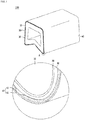
- FIG. 1 illustrates embodiment of an electric contacting terminal according to an embodiment of the present invention.
- An elastic electric contact terminal 100 is formed in which a core 10, an adhesive layer 20, a polymer film 30, and a metal layer 40 are sequentially laminated.
- the electric contact terminal 100 is interposed between a circuit board and an electroconductive object to electrically connect therebetween, and may be installed by being forcibly inserted between a conductive pattern of the circuit board and the electroconductive object or be soldered with a solder cream to the conductive pattern of the circuit board to contact a facing electroconductive object.
- the electric contact terminal 100 is reel-taped to a carrier and reflow-soldered using vacuum pick-up and a solder cream.
- the core 10 of a rubber material has heat resistance and elasticity and may be electrically insulated. Consequently, the core 10 may be formed of a non-foaming silicon rubber or a foam rubber, for example, a sponge, which has a tube shape and satisfies reflow-soldering and an elastic condition, but is not limited thereto.
- the core 10 may be made by, for example, an extrusion process and is formed symmetrically to be balanced in a horizontal direction at the time of soldering to reduce lifting or deviation phenomenon at the time of reflow-soldering with a solder cream.
- the core 10 may have a shape that one or more penetration holes are formed in the tube or inside in a longitudinal direction, or may not have a penetration hole like a sponge.
- the thicknesses of both sidewalls of the penetration hole of the core 10 may be formed thinner than those of upper and lower sidewalls to have good elasticity and to make a user exert less force to press.
- a cross section of the core 10 has a tube shape or a shape with a penetration hole therein, if the height of the electric contact terminal 100 is equal to or smaller than 0.5 mm, it is hard to form the penetration hole and to make the shape in a tube type, and a making efficiency is also degraded.
- FIGS. 2(a) and 2(b) show modification examples of a core.
- a pair of channels 211 and 212 caved in downward from the top surface and having a constant width and depth are formed apart and extend along a longitudinal direction, and as a result, a support wall 218 is formed at the approximately same height as that of the sidewalls 214 and 216 between the channels 211 and 212.
- the bottoms of the channels 211 and 212 may be formed to have slopes similarly to the bottom surface of the core 210 and have upward slopes from outer bottom corners toward inner sides.
- the sidewalls 214 and 216 are respectively formed in the outsides of the channels 211 and 212 and the support wall 218 is formed therein and accordingly, an object to be pressed upward is supported by the sidewalls 214 and 216 and the support wall 218.
- the cross section shape of the support wall 218 is not particularly limited, but may be, for example, a trapezoidal shape that becomes smaller as proceeding toward the top surface and both corners of the top surface may be formed round.
- the both sidewalls 214 and 216 may be formed in a shape that outer sides of the top surface are round-treated, and this allows a completed electric contact terminal to be easily pressed inside, when being pressed by a facing object after being soldered to a printed circuit board, etc., and prevents an external object from being stuck to both side corners.
- a single channel may be formed and a separate support wall may not be formed.
- multiple channels may be formed and in this case, multiple support walls 218 may be formed between the channels.
- the core 210 is formed in a small size of, for example, the width of 2 mm, the height of 0.5 mm, and the length of 1 mm, but is not limited thereto and has a size equal to or smaller than that.
- the core 210 of such a size when forming a penetration hole therein as usual or making a core 210 itself in a tube shape, it is hard to make the height equal to or smaller than 0.7 mm.
- an electric contact terminal in which the height is equal to or smaller than 0.5 mm may be easily made, since the core 210 is caved downward from the top surface to form the channels 211 and 212 having a constant width and depth and extending in a longitudinal direction.
- the polymer film 30 in which the metal layer 40 is laminated on the top surface may wrap the core 210 to span the both sidewalls 214 and 216 and the support wall 218 as shown in FIG. 2(a) or wrap the core 210 to closely adhere to an outer surface of the core 210 as shown in FIG. 2(b) .
- the top surface of the support wall 218 has an adhesive layer 220 intervened like other parts of the core 210 to adhere to the polymer film 230 and prevents the polymer film 230 from being lifted.
- the bottom surface of the core 10 may be formed obliquely to be caved in from the both ends toward the central part in a transverse direction.
- the bottom surface of the core 10 may be formed obliquely to be caved in from both corners in the transverse direction toward the center part in order to form the hypotenuse of an isosceles triangle of the core 10 when the core 10 is vertically cut off.
- the slope angle is not particularly limited but it is sufficient that a space is formed which accommodates an adhesive leaked out from the adhesive layer 20 at the bottom portion of the bottom surface of the core 10 and does not affect soldering.
- both sides of the bottom surface of the electric contact terminal 100 may uniformly contact molten solder at the time of reflow-soldering to prevent a lifting phenomenon that only any one part of the bottom surface is soldered.
- the bottom surface of the core 10 has a shape caved in from the both ends toward the central part, a space capable of accommodating the adhesive leaked out externally from the adhesive layer 20 is provided to minimize a phenomenon that soldering is not performed at the time of reflow-soldering in the making process.
- the adhesive layer 20 has flexibility, elasticity, and insulation, and also may have heat resistance when the electric contact terminal 100 is applied to reflow-soldering, and may be located between the core 10 and the polymer film 30 to reliably adhere to the core 10 and the polymer film 30.
- the adhesive layer 20 may be formed by thermal curing of, for example, a liquid silicon rubber, and the liquid silicon rubber adheres to a facing object while being cured and forms the adhesive layer 20 in a solid state after being cured. Once being cured, the adhesive layer 20 maintains elasticity, is not molten even when heat is applied again and maintains adhesion even at the time of soldering.
- the adhesive layer 20 may be formed when a silicon rubber adhesive having self-adhesion is cured and the thickness thereof is about 0.005 mm to about 0.03 mm.
- the polymer film 30 may be, for example, a polyimide (PI) film having good heat resistance or another heat-resistant polymer film and the thickness thereof may be determined in consideration of flexibility or a mechanical strength.
- PI polyimide
- the polymer film 30 is a typical polymer film used in a flexible circuit board having flexibility.
- the polymer film 30 may be formed by curing after a liquid polymer is cast and the thickness of the cured polymer film 30 is about 0.007 mm to 0.030 mm.
- the metal layer 40 is formed such that one surface thereof wraps and adheres to the polymer film 30 and a metal plating layer 42 is formed to cover a copper layer 41.
- the metal plating layer 42 is formed on the entire exposed surface of the copper layer 41 and the exposed surface includes a surface of the copper layer 41, namely, a top surface, a side surface, and a bottom surface, and includes a cross section and both sections in a transverse direction.
- the copper layer 41 may be a copper foil of an electrolytic copper foil or a rolled copper foil, or typically indicate a copper plating layer formed on a resultant obtained after tungsten is sputtered as a seed onto one surface of the polymer film.
- the copper foil will be exemplified for convenience of explanation.
- the thickness of the copper foil 41 is about 10 ⁇ m and the copper plating layer is thinly formed to have the thickness of about 3 ⁇ m
- the metal plating layer 42 is less corrosive, i.e. less prone to corrosion, than the copper foil 41, and the copper foil 41 is thicker than the metal plating layer 42.
- the copper foil 41 may adhere to the polymer film 30 with an adhesive intervened therebetween or may adhere by coating and curing a liquid polymer corresponding to the polymer film 30 on the copper foil 41 such that the metal layer 40 is formed to wrap and adhere to the polymer film 30.
- the metal plating layer 42 is formed by plating with tin (Sn) or silver (Ag) or plating with nickel (Ni) and then with tin (Sn) or gold (Au) and the thickness of tin or silver may be about 2 ⁇ m and the thickness of nickel or gold is equal to or smaller than about 1 ⁇ m
- the metal plating layer 42 is formed such that corrosion of the surface of the copper foil 41 is prevented or the surface of the copper foil 41 is electrified and well soldered. According to this embodiment, as magnified and illustrated within a circle in FIG. 1 , the metal plating layer 42 is formed on and covers the copper foil 41 exposed at the cross section of the contact terminal 100.
- a boundary between the copper foil 41 and the metal plating layer 42 is denoted by a dotted line and the copper foil 41 is illustrated to be covered at the cross section by the metal plating layer 42.
- the copper foil is typically exposed externally at the cross section formed by a cutoff, the copper foil exposed in a reliability test like a saltwater spray test contacts saltwater to cause corrosion. Therefore, the copper foil does not pass the saltwater spray test or corrosion occurs on the exposed copper foil in use to result in reliability degradation.
- the contact with the saltwater may be fundamentally blocked in the reliability test.
- the copper foil 41 in use is not exposed, there is no concern about occurrence of corrosion and reliability is enhanced.
- solder cream may spread better on the metal plating layer 42 formed to cover the copper foil 41 at the cross section at the time of reflow-soldering, the soldering strength may be increased and especially the soldering strength is enhanced at the cross section.
- the soldering strength at the cross section is very important and the present invention is very useful in this case.
- the metal plating layer 42 is not formed on the adhesive pressed out externally, an appearance of the electric contact terminal 100, in particular, the top surface and bottom surface may be easily discerned with the naked eye.
- the contact terminal bar is cut to a uniform length, for example, about 500 mm, when the contact terminal bar is provided by the polymer film 30, of which one side has the copper foil 41 adhering thereto, consecutively wrapping the core 10 with the liquid-phased adhesive layer 20 intervened therebetween.
- the contact terminal bar is cut to a length desired by a customer, for example, about 3 mm to form a contact terminal and as described above, the final contact terminal 100 is made by forming the metal plating layer 42 plated with tin, silver, or nickel/gold to cover the exposed surface of the copper foil 41.
- the specific gravity of the contact terminal 100 is smaller than that of water due to the core 10 of a silicon rubber material, and thus the metal plating layer 42 may be formed using electroless plating in a bulk manner.
- the forming manner is not limited thereto and electrolytic plating may also be applied thereto.
- the surface roughness of the metal plating layer 42 is increased to cause the surface to be rough, which enhances adhesion to the solder cream and increases the soldering strength.
- the core 10 is made of a non-foaming silicon rubber or foam rubber, for example, sponge
- the adhesive layer 20 is formed by thermal-curing a liquid silicon rubber
- the polymer film 30 is formed of a polyimide film
- the metal plating layer 42 is not formed on the cross section by a plating process.
- the metal plating layer 42 is formed on all the externally exposed copper foil 41 including the surface, the cross section, and both sections in the transverse direction and the copper foil 41 is blocked from the outside.
- a product in which the metal plating layer 42 is formed is automatically reel-taped on a carrier tape using a reel taping device.
- the electric contact terminal 100 of the present invention may fundamentally block contact from saltwater in the reliability test by covering all the copper foil 41 with the metal plating layer 42, there is no concern about occurrence of corrosion thereon, and the solder cream spreads well on the cross section to increase the soldering strength at the time of reflow soldering.
- the metal plating layer 42 is also formed on both sections in the transverse direction of the copper foil 41 positioned on the bottom surface of the core 10 and consequently the copper foil 41 is not exposed externally at all.
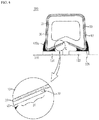
- FIG. 3 illustrates a state where an electric contact terminal is soldered on a circuit board
- an electric contact terminal 200 is disclosed of which the width of 2 mm is longer than the length of 1mm.
- the electric contact terminal 200 is soldered with the solder cream 120 intervened on the conductive pattern 110 of the circuit board, and the solder cream 120 spreads along the side surface of the copper foil 41 and along a metal plating layer part 42a covering the copper foil 41 at the cross section of the contact terminal 200.
- solder cream 120 extends along the metal plating layer part 42a covering the copper foil 41 at the cross section of the electric contact terminal 200, lead rising and solderability are enhanced and consequently a soldering strength is enhanced.
- FIG. 4 illustrates an electric contact terminal according to another non-claimed embodiment of the present invention
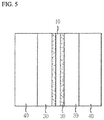
- FIG. 5 illustrates the bottom surface of the electric contact terminal
- FIG. 6 illustrates a state where an electric contact terminal is mounted on a circuit board
- FIG. 6(a) shows an electric contact terminal of the present invention
- FIG. 6(b) shows a typical electric contact terminal.
- the metal layer 40 is partially removed from both ends and a certain part 31 is exposed externally from both ends of the polymer film 30.
- the metal layer 40 may be removed to be exposed from the both ends of the polymer film 30 as much as a width of 0.05 mm to 0.3 mm, and the removed width of the metal layer 40 may be differed according to the width of the contact terminal 300. In other words, it should be considered that as the removed width of the metal layer 40 increases, a soldered area becomes relatively reduced and consequently decrease the soldering strength.
- the metal layer 40 is removed from both ends of the polymer film 30 by a certain length in a transverse direction and consecutively in a longitudinal direction, and then the polymer film 30 is exposed externally.
- the contact terminal 300 since the area of the metal layer 40 formed on the bottom surface of the contact terminal 300 is decreased, when an identical amount of the solder cream is applied in an identical solder pattern to the contact terminal 300 of an identical configuration, an amount of a molten solder cream spreading along the metal layer 40 on the bottom surface of the contact terminal 300 is decreased. Therefore, the molten solder cream spreads relatively greatly along a side surface and consequently a solder fillet 120a may be formed to a higher position to reliably support the side surface of the contact terminal 300 after soldering. As a result, the contact terminal 300 may strongly respond to a force applied thereto from a later direction.
- both end portions of the metal layer 40 are positioned at an inner side than both end portions of the polymer film 30, when the contact terminal 300 is made by curing after the elastic core 10 is wrapped with the polymer film 30 with a liquid polymer adhesive intervened therebetween, a tendency that the both end portions of the polymer film 30 are detached from the core 10 by an elastic recovery force of the metal layer 40 before the polymer adhesive is completely cured may be greatly reduced.
- a step formed by the both end portions of the copper foil 41 may block the flow of the adhesive to enhance the soldering strength and to reduce a lifting phenomenon.
- the area occupied by the metal layer 40 bended toward the bottom surface of the contact terminal 300 is reduced, the area occupied by the solder cream on the bottom surface of the contact terminal 300 becomes reduced to consequently form a space having a relatively larger volume at the bottom surface of the contact terminal. Therefore, a force applied from the outside may be elastically received.
- a portion corresponding to a certain part 31 of the polymer film 30 may be removed by lithography and etching processes, for example, in a state where the copper foil 41 is formed on the polymer film 30.
- the metal plating layer 42 is formed by plating with tin or silver, or with tin or gold after nickel-plating on the copper foil 41.
- the molten solder cream spreads along the metal layer 40 wrapping the bottom surface and side surface of the contact terminal. Since both end portions of the polymer film 30 are identical to the both end portions of the metal layer 40 and the molten solder cream mainly spreads along the metal layer 40 formed at the bottom surface, solder fillets 122 and 122a having a relatively small size are formed at the side surface.
- the contact terminal since not sufficiently responding to a force applied from a lateral direction, the contact terminal may be easily detached from conductive patterns 110 and 112.
- the metal layer 40 on the bottom surface is pulled downward by the molten solder cream in the soldering process, both end portions of the polymer film 30 adhering to the core 10 become lifted and detached by a unique recovery force of the metal layer 40 and a pulling force by the molten solder cream.
- the solder fillet 120a formed on the side surface of the contact terminal 300 may sufficiently respond thereto and reduce detachment of the contact terminal 300 from the conductive patterns 110 and 112.
- the metal layer 40 on the bottom surface is pulled downward by the solder cream molten at the time of soldering. Since the both end portions of the metal layer 40 are positioned at an inner side than the both end portions of the polymer film 30, a pulling force by the molten solder cream is reduced and an area of the metal layer 40 is reduced to decrease a unique elastic recovery force. At a result, a phenomenon that the both end portions of the polymer film 30 attached to the core 10 are pulled downward by the metal layer 40 and lifted to be detached may be prevented.
- the electric contact terminal 100, 200 or 300 is soldered by the solder cream and contacts a facing electrical conductive object
- the present invention is not limited thereto and like the above description, the electric contact terminal 100, 200 or 300 may be installed by being forcibly inserted between a conductive pattern and an electrical conductive object of the circuit board.
- a material of an element is not necessary to have heat-resistance.
- a contact between saltwater and a copper foil may be basically blocked in a reliability test by covering the copper foil exposed at a cross section in a longitudinal direction with a metal plating layer having a good environmental resistance, and reliability is improved, since the copper foil in use is not exposed externally to remove a concern about rust.
- solder cream spreads well on a metal plating layer formed to cover the copper foil at the longitudinal cross section to result in an increase in soldering strength.
- a solder fillet may be formed to a relatively higher position of the contact terminal to resist against a force laterally applied to the contact terminal as a result.
Landscapes
- Engineering & Computer Science (AREA)
- Manufacturing & Machinery (AREA)
- Microelectronics & Electronic Packaging (AREA)
- Coupling Device And Connection With Printed Circuit (AREA)
- Manufacturing Of Electrical Connectors (AREA)
Description
- The present invention relates to an elastic electric contact terminal, and more particularly, to an elastic electric contact terminal which is less corrosive and of which the environmental resistance is improved and the soldering strength is reliably improved.
- Typically, an elastic electric contact terminal on which soldering is possibly performed is required to have a good electric conductivity, a good elastic recovery force, and a high tolerance to a soldering temperature.
- As an example of the elastic electric contact terminal, Korean Patent No.
783588 - In addition, Korean Patent No.
1001354 - In the above-described process of fabricating the electric contact terminal, a rolled silicon rubber is provided, a liquid silicon rubber adhesive is consecutively placed thereon in a longitudinal direction of the silicon rubber, a polymer film in which a metal layer is formed is wrapped to expose the metal layer outside on the liquid silicon rubber adhesive, and then the silicon rubber adhesive is cured to adhere to the polymer film. Then the resultant is cut to a uniform length of, for example, 500 mm and cut again in a length of, for example, 3 mm required by a customer. Thereafter the resultant product plated with a metal is reel-taped.
- Here, the metal layer is formed by plating a copper foil with tin or silver or plating a copper foil with nickel and then with tin or gold thereon, and the thickness of the copper foil is about 0.01 mm, which is significantly thicker than that of tin, silver, nickel or gold.
- In this way, a metal plating layer of which environmental resistance is better than that of copper is formed on a copper foil of an existing contact terminal such that corrosion is prevented and soldering with a solder cream is well performed, but during a process for fabricating the contact terminal, the contact terminal is cut off to a length required by a customer. Therefore, the copper foil is only to be exposed outside at a cross section formed on a side in a longitudinal direction of the contact terminal.
- In other words, since an existing contact terminal is made by wrapping a core in a polymer film having a copper foil plated with a metal layer such as tin and then is cut off, the copper foil is only to be exposed outside at the cross section.
- As a result, there occurs a limitation in that the contact terminal may not pass a reliability test such as a saltwater spray test, since saltwater contacts the externally exposed copper foil to corrode the contact terminal, or in that the externally exposed copper foil is easily rusted to result in quality degradation.
- In addition, there is a shortcoming that when the contact terminal is reflow-soldered to be mounted on a circuit board, since the copper foil is exposed at an externally exposed cross section, a lead-rising phenomenon occurs less on the copper foil than on the metal plating layer, which results in a less strong soldering strength at the cross section.
- In addition, since the copper foil wrapping and adhering to the polymer film is bended at both bottom ends of the core, the bended copper foil always receives an elastic recovery force caused by an attempt to return to an original position, although the magnitude is small. There is also a limitation in that when the contact terminal is mounted on a circuit board by reflow-soldering, the melted soldering cream is applied to the copper foil to pull the copper foil downward and the pulling force is added to the elastic recovery force of the copper foil itself, thereby both ends of the polymer film being detached from the core or the adhesive.
- Similarly, it is highly possible that both end parts of the polymer film are lifted and detached from the core or the adhesive before the adhesion is completed, when the polymer film and core are adhered with the adhesive in a making process.
- Further, patent document
KR 2015 0020043 A - An object of the present invention is to provide an elastic electric contact terminal which is robust against corrosion.
- Another object of the present invention is to provide an elastic electric contact terminal of which a soldering strength is improved and soldering reliability is improved.
- A further another object of the present invention is to provide an elastic electric contact terminal having a soldering strength capable of strongly resisting against a laterally applied external force.
- A still further another object is to provide an elastic electric contact terminal capable of minimizing detachment of both ends of the polymer film during a making process or after soldering.
- The above objects are solved by the subject-matter of claim 1. Further advantageous configurations of the invention can be drawn from the dependent claims.
- According to an aspect of the present disclosure, there is provided an elastic electric contact terminal including: an elastic core; a polymer film wrapping and adhering to the core with an adhesive layer intervened therebetween; and a solderable copper foil wrapping and adhering to the polymer film, wherein a metal plating layer is formed on all surfaces exposed outside the copper foil.
- A specific gravity of the electric contact terminal is smaller than that of water.
- Preferably, the metal plating layer may be formed by plating with tin (Sn) or silver (Ag), or by plating with tin (Sn) or gold (Au) after plating with nickel (Ni).
- The metal plating layer has less corrosiveness than the copper foil.
- Preferably, the copper foil may be thicker than the metal plating layer.
- Preferably, the copper foil may be an electrolytic copper foil or a rolled copper foil, and adheres to the polymer film by coating, on the copper foil, and curing a liquid polymer corresponding to the polymer film, or adheres to the polymer film with an adhesive intervened therebetween.
- Preferably, soldering may be performed easier on the metal plating layer than on the copper foil at a time of the soldering.
- Preferably, the elastic core may be a silicon rubber in a tube type or foam type, the adhesive layer may be a silicon rubber adhesive layer, and the polymer film may be polyimide (PI).
- Preferably, the metal plating layer may be formed by electroless plating to increase a surface roughness, and thus a soldering strength may be enhanced.
- Preferably, the electric contact terminal may have a width longer than a length.
- Preferably, the electric contact terminal may be soldered to a conductive pattern of a circuit board with a solder cream and may be elastically electrically connected to a facing electrical conductive object.
- The exposed surfaces include a surface and both sections in a transverse direction of the copper foil, and a cross section of the copper foil, which may be formed by cutting the electric contact terminal.
- Preferably, the metal layer may be removed by a prescribed part from both ends of the polymer film at a bottom surface of the core and exposed externally.
- Preferably, the metal layer may be removed by a prescribed width in a transverse direction and consecutively in a longitudinal direction from the both ends of the polymer film at the bottom surface of the core.
- Preferably, the metal layer may be formed by lithographing and etching.
- Preferably, the core may be formed caved downward in a prescribed width and depth from a top surface, and may include at least one channel extending along a longitudinal direction.
- Preferably, the polymer film may cross the channel to extend over the both sidewalls or closely adhere to an outer surface of the core, and the both sidewalls of the channel elastically may support the object.
- Preferably, the channel may be formed in plurality and a support wall protruding between the channels to a height corresponding to the both sidewalls and extending in the longitudinal direction is further included.
- Preferably, a top surface of the support wall may adhere to the polymer film with the adhesive layer intervened therebetween.
- Preferably, a side surface of a channel side of the both sidewalls may have a slope and the both sidewalls may tilt toward the channel side at a time of being pressurized by the object.
- According to another ; non-claimed aspect of the present disclosure, there is provided an elastic electric contact terminal including: an elastic core; a polymer film wrapping and adhering to the core with an adhesive layer intervened therebetween; and a solderable metal layer wrapping and adhering to the polymer film, wherein the metal layer includes a copper plating layer formed by plating after a metal seed is sputtered on the polymer film, and the metal plating layer is formed to cover a surface and both sections in a transverse direction of the copper plating layer, and a cross section of the copper plating layer formed by cutting the electric contact terminal.
- According to still another ; non-claimed aspect of the present disclosure, there is provided a method for making an elastic electric contact terminal, the method including: providing a rolled silicon rubber; consecutively coating a liquid silicon rubber adhesive in a longitudinal direction of the silicon rubber; wrapping the silicon rubber with one surface of a polymer film with the liquid silicon rubber adhesive intervened therebetween and another surface of the polymer film adhered to by a copper foil, and curing the silicon rubber adhesive to make the polymer film adhere to the silicon rubber and to form a laminated body; cutting the laminated body to a prescribed length; and plating, with a metal, a surface and both sections in a transverse direction of the copper foil and a cross section of the copper foil, which is formed by the cutting, and forming a metal plating layer.
- The above objects and other advantages of the present invention will become more apparent by describing in detail exemplary embodiments thereof with reference to the attached drawings in which:
-
FIG. 1 illustrates an electric contact terminal according to an embodiment of the present invention. -
FIGS. 2(a) and 2(b) show modification examples of a core. -
FIG. 3 illustrates a state where an electric contact terminal is soldered on a circuit board -
FIG. 4 illustrates an electric contact terminal. -
FIG. 5 illustrates a bottom surface of the electric contact terminal ofFIG. 4 . -
FIG. 6 illustrates states where an electric contact terminal is mounted on a circuit board,FIG. 6(a) illustrates an electric contact terminal according to the present invention, andFIG. 6(b) illustrates a typical electric contact terminal. - Hereinafter, specific embodiments will be described in detail with reference to the accompanying drawings.
-
FIG. 1 illustrates embodiment of an electric contacting terminal according to an embodiment of the present invention. - An elastic
electric contact terminal 100 is formed in which acore 10, anadhesive layer 20, apolymer film 30, and ametal layer 40 are sequentially laminated. - The
electric contact terminal 100 is interposed between a circuit board and an electroconductive object to electrically connect therebetween, and may be installed by being forcibly inserted between a conductive pattern of the circuit board and the electroconductive object or be soldered with a solder cream to the conductive pattern of the circuit board to contact a facing electroconductive object. - For a reflow soldering, the
electric contact terminal 100 is reel-taped to a carrier and reflow-soldered using vacuum pick-up and a solder cream. - The
core 10 of a rubber material has heat resistance and elasticity and may be electrically insulated. Consequently, thecore 10 may be formed of a non-foaming silicon rubber or a foam rubber, for example, a sponge, which has a tube shape and satisfies reflow-soldering and an elastic condition, but is not limited thereto. - The core 10 may be made by, for example, an extrusion process and is formed symmetrically to be balanced in a horizontal direction at the time of soldering to reduce lifting or deviation phenomenon at the time of reflow-soldering with a solder cream.
- By providing a plane for vacuum pick-up to a top surface of the
core 10 and forming respectively both side corners of the top surface in a round shape, it is not only easy to handle but also able to prevent theelectric contact terminal 100 from being stuck at the both corners in a process that the completedelectric contact terminal 100 is assembled with a facing object after being soldered to a printed circuit board etc. - The core 10 may have a shape that one or more penetration holes are formed in the tube or inside in a longitudinal direction, or may not have a penetration hole like a sponge.
- The thicknesses of both sidewalls of the penetration hole of the core 10 may be formed thinner than those of upper and lower sidewalls to have good elasticity and to make a user exert less force to press.
- On the other hand, when a cross section of the
core 10 has a tube shape or a shape with a penetration hole therein, if the height of theelectric contact terminal 100 is equal to or smaller than 0.5 mm, it is hard to form the penetration hole and to make the shape in a tube type, and a making efficiency is also degraded. -
FIGS. 2(a) and 2(b) show modification examples of a core. - In the
core 110, a pair ofchannels support wall 218 is formed at the approximately same height as that of thesidewalls channels - The bottoms of the
channels core 210 and have upward slopes from outer bottom corners toward inner sides. - According to the above-described structure, the
sidewalls channels support wall 218 is formed therein and accordingly, an object to be pressed upward is supported by thesidewalls support wall 218. - The cross section shape of the
support wall 218 is not particularly limited, but may be, for example, a trapezoidal shape that becomes smaller as proceeding toward the top surface and both corners of the top surface may be formed round. - As the above-described embodiment, the both
sidewalls - In this embodiment, although an example of forming the pair of
channels multiple support walls 218 may be formed between the channels. - The
core 210 is formed in a small size of, for example, the width of 2 mm, the height of 0.5 mm, and the length of 1 mm, but is not limited thereto and has a size equal to or smaller than that. - As described above, for the
core 210 of such a size, when forming a penetration hole therein as usual or making acore 210 itself in a tube shape, it is hard to make the height equal to or smaller than 0.7 mm. However in this embodiment, an electric contact terminal in which the height is equal to or smaller than 0.5 mm may be easily made, since thecore 210 is caved downward from the top surface to form thechannels - Side surfaces of the both
sidewalls channels channels sidewalls channels - On the other hand, the
polymer film 30 in which themetal layer 40 is laminated on the top surface may wrap thecore 210 to span the bothsidewalls support wall 218 as shown inFIG. 2(a) or wrap thecore 210 to closely adhere to an outer surface of the core 210 as shown inFIG. 2(b) . - For
FIG. 2(a) , the top surface of thesupport wall 218 has an adhesive layer 220 intervened like other parts of the core 210 to adhere to the polymer film 230 and prevents the polymer film 230 from being lifted. - The bottom surface of the core 10 may be formed obliquely to be caved in from the both ends toward the central part in a transverse direction. In other words, the bottom surface of the core 10 may be formed obliquely to be caved in from both corners in the transverse direction toward the center part in order to form the hypotenuse of an isosceles triangle of the core 10 when the
core 10 is vertically cut off. - The slope angle is not particularly limited but it is sufficient that a space is formed which accommodates an adhesive leaked out from the
adhesive layer 20 at the bottom portion of the bottom surface of thecore 10 and does not affect soldering. - According to such a structure, since the bottom surface of the
core 10 has a shape to be caved in from the both ends toward the central part, both sides of the bottom surface of theelectric contact terminal 100 may uniformly contact molten solder at the time of reflow-soldering to prevent a lifting phenomenon that only any one part of the bottom surface is soldered. - In addition, since the bottom surface of the
core 10 has a shape caved in from the both ends toward the central part, a space capable of accommodating the adhesive leaked out externally from theadhesive layer 20 is provided to minimize a phenomenon that soldering is not performed at the time of reflow-soldering in the making process. - The
adhesive layer 20 has flexibility, elasticity, and insulation, and also may have heat resistance when theelectric contact terminal 100 is applied to reflow-soldering, and may be located between the core 10 and thepolymer film 30 to reliably adhere to thecore 10 and thepolymer film 30. - The
adhesive layer 20 may be formed by thermal curing of, for example, a liquid silicon rubber, and the liquid silicon rubber adheres to a facing object while being cured and forms theadhesive layer 20 in a solid state after being cured. Once being cured, theadhesive layer 20 maintains elasticity, is not molten even when heat is applied again and maintains adhesion even at the time of soldering. - The
adhesive layer 20 may be formed when a silicon rubber adhesive having self-adhesion is cured and the thickness thereof is about 0.005 mm to about 0.03 mm. - The
polymer film 30 may be, for example, a polyimide (PI) film having good heat resistance or another heat-resistant polymer film and the thickness thereof may be determined in consideration of flexibility or a mechanical strength. - The
polymer film 30 is a typical polymer film used in a flexible circuit board having flexibility. - For example, the
polymer film 30 may be formed by curing after a liquid polymer is cast and the thickness of the curedpolymer film 30 is about 0.007 mm to 0.030 mm. - The
metal layer 40 is formed such that one surface thereof wraps and adheres to thepolymer film 30 and ametal plating layer 42 is formed to cover acopper layer 41. - In other words, the
metal plating layer 42 is formed on the entire exposed surface of thecopper layer 41 and the exposed surface includes a surface of thecopper layer 41, namely, a top surface, a side surface, and a bottom surface, and includes a cross section and both sections in a transverse direction. - Here, the
copper layer 41 may be a copper foil of an electrolytic copper foil or a rolled copper foil, or typically indicate a copper plating layer formed on a resultant obtained after tungsten is sputtered as a seed onto one surface of the polymer film. Hereinafter the copper foil will be exemplified for convenience of explanation. - The thickness of the
copper foil 41 is about 10 µm and the copper plating layer is thinly formed to have the thickness of about 3 µm - It is necessary to take a notice that the
metal plating layer 42 is less corrosive, i.e. less prone to corrosion, than thecopper foil 41, and thecopper foil 41 is thicker than themetal plating layer 42. - The
copper foil 41 may adhere to thepolymer film 30 with an adhesive intervened therebetween or may adhere by coating and curing a liquid polymer corresponding to thepolymer film 30 on thecopper foil 41 such that themetal layer 40 is formed to wrap and adhere to thepolymer film 30. - The
metal plating layer 42 is formed by plating with tin (Sn) or silver (Ag) or plating with nickel (Ni) and then with tin (Sn) or gold (Au) and the thickness of tin or silver may be about 2µm and the thickness of nickel or gold is equal to or smaller than about 1µm - The
metal plating layer 42 is formed such that corrosion of the surface of thecopper foil 41 is prevented or the surface of thecopper foil 41 is electrified and well soldered. According to this embodiment, as magnified and illustrated within a circle inFIG. 1 , themetal plating layer 42 is formed on and covers thecopper foil 41 exposed at the cross section of thecontact terminal 100. - In
FIG. 1 , a boundary between thecopper foil 41 and themetal plating layer 42 is denoted by a dotted line and thecopper foil 41 is illustrated to be covered at the cross section by themetal plating layer 42. - Accordingly, since the copper foil is typically exposed externally at the cross section formed by a cutoff, the copper foil exposed in a reliability test like a saltwater spray test contacts saltwater to cause corrosion. Therefore, the copper foil does not pass the saltwater spray test or corrosion occurs on the exposed copper foil in use to result in reliability degradation.
- However, according to the present invention, since the
copper foil 41 exposed at the cross section is covered with themetal plating layer 42, the contact with the saltwater may be fundamentally blocked in the reliability test. In addition, since thecopper foil 41 in use is not exposed, there is no concern about occurrence of corrosion and reliability is enhanced. - Furthermore, since the solder cream may spread better on the
metal plating layer 42 formed to cover thecopper foil 41 at the cross section at the time of reflow-soldering, the soldering strength may be increased and especially the soldering strength is enhanced at the cross section. - In particular, when the width of the
contact terminal 100 is longer the length, the soldering strength at the cross section is very important and the present invention is very useful in this case. - In addition, since the
metal plating layer 42 is not formed on the adhesive pressed out externally, an appearance of theelectric contact terminal 100, in particular, the top surface and bottom surface may be easily discerned with the naked eye. - In order to make the
electric contact terminal 100 according to the embodiment, the contact terminal bar is cut to a uniform length, for example, about 500 mm, when the contact terminal bar is provided by thepolymer film 30, of which one side has thecopper foil 41 adhering thereto, consecutively wrapping the core 10 with the liquid-phasedadhesive layer 20 intervened therebetween. - Thereafter, the contact terminal bar is cut to a length desired by a customer, for example, about 3 mm to form a contact terminal and as described above, the
final contact terminal 100 is made by forming themetal plating layer 42 plated with tin, silver, or nickel/gold to cover the exposed surface of thecopper foil 41. - Here, the specific gravity of the
contact terminal 100 is smaller than that of water due to thecore 10 of a silicon rubber material, and thus themetal plating layer 42 may be formed using electroless plating in a bulk manner. However, the forming manner is not limited thereto and electrolytic plating may also be applied thereto. - In particular, when the
metal plating layer 42 is formed by the electroless plating, the surface roughness of themetal plating layer 42 is increased to cause the surface to be rough, which enhances adhesion to the solder cream and increases the soldering strength. - As the above description, since the
core 10 is made of a non-foaming silicon rubber or foam rubber, for example, sponge, theadhesive layer 20 is formed by thermal-curing a liquid silicon rubber, and thepolymer film 30 is formed of a polyimide film, themetal plating layer 42 is not formed on the cross section by a plating process. - As the above description, for the
electric contact terminal 100, themetal plating layer 42 is formed on all the externally exposedcopper foil 41 including the surface, the cross section, and both sections in the transverse direction and thecopper foil 41 is blocked from the outside. - Thereafter, a product in which the
metal plating layer 42 is formed is automatically reel-taped on a carrier tape using a reel taping device. - In this way, since the
electric contact terminal 100 of the present invention may fundamentally block contact from saltwater in the reliability test by covering all thecopper foil 41 with themetal plating layer 42, there is no concern about occurrence of corrosion thereon, and the solder cream spreads well on the cross section to increase the soldering strength at the time of reflow soldering. - In particular, since the plating process is performed on the
entire copper foil 41 exposed externally after the cutoff, themetal plating layer 42 is also formed on both sections in the transverse direction of thecopper foil 41 positioned on the bottom surface of thecore 10 and consequently thecopper foil 41 is not exposed externally at all. -
FIG. 3 illustrates a state where an electric contact terminal is soldered on a circuit board - In this non-claimed embodiment, an
electric contact terminal 200 is disclosed of which the width of 2 mm is longer than the length of 1mm. - As illustrated in a magnified circle of
FIG. 3 , theelectric contact terminal 200 is soldered with thesolder cream 120 intervened on theconductive pattern 110 of the circuit board, and thesolder cream 120 spreads along the side surface of thecopper foil 41 and along a metalplating layer part 42a covering thecopper foil 41 at the cross section of thecontact terminal 200. - As a result, since the
solder cream 120 extends along the metalplating layer part 42a covering thecopper foil 41 at the cross section of theelectric contact terminal 200, lead rising and solderability are enhanced and consequently a soldering strength is enhanced. - In particular, for the
electric contact terminal 200 of which the width is longer than the length, since an area occupied by the metalplating layer part 42a is increased as the width increases, reliability and performance of theelectric contact terminal 200 are improved to increase the soldering strength at the time of reflow soldering as the lead-rising and solderability are enhanced. -
FIG. 4 illustrates an electric contact terminal according to another non-claimed embodiment of the present invention,FIG. 5 illustrates the bottom surface of the electric contact terminal,FIG. 6 illustrates a state where an electric contact terminal is mounted on a circuit board,FIG. 6(a) shows an electric contact terminal of the present invention, andFIG. 6(b) shows a typical electric contact terminal. - At the bottom surface of a
contact terminal 300, themetal layer 40 is partially removed from both ends and acertain part 31 is exposed externally from both ends of thepolymer film 30. - For example, the
metal layer 40 may be removed to be exposed from the both ends of thepolymer film 30 as much as a width of 0.05 mm to 0.3 mm, and the removed width of themetal layer 40 may be differed according to the width of thecontact terminal 300. In other words, it should be considered that as the removed width of themetal layer 40 increases, a soldered area becomes relatively reduced and consequently decrease the soldering strength. - In other words, from views of
FIG. 5 and an inside of a magnified circle of C inFIG. 4 , themetal layer 40 is removed from both ends of thepolymer film 30 by a certain length in a transverse direction and consecutively in a longitudinal direction, and then thepolymer film 30 is exposed externally. - According to such a configuration, since the area of the
metal layer 40 formed on the bottom surface of thecontact terminal 300 is decreased, when an identical amount of the solder cream is applied in an identical solder pattern to thecontact terminal 300 of an identical configuration, an amount of a molten solder cream spreading along themetal layer 40 on the bottom surface of thecontact terminal 300 is decreased. Therefore, the molten solder cream spreads relatively greatly along a side surface and consequently asolder fillet 120a may be formed to a higher position to reliably support the side surface of thecontact terminal 300 after soldering. As a result, thecontact terminal 300 may strongly respond to a force applied thereto from a later direction. - In addition, since both end portions of the
metal layer 40 are positioned at an inner side than both end portions of thepolymer film 30, when thecontact terminal 300 is made by curing after theelastic core 10 is wrapped with thepolymer film 30 with a liquid polymer adhesive intervened therebetween, a tendency that the both end portions of thepolymer film 30 are detached from the core 10 by an elastic recovery force of themetal layer 40 before the polymer adhesive is completely cured may be greatly reduced. - In addition, since an area to which the molten solder cream adheres is also decreased as an area occupied by the
metal layer 40 bended toward the bottom surface of thecontact terminal 300 is decreased, a force for pulling, by the molten solder cream, thecopper foil 41 downward is also decreased to prevent the both end portions of thepolymer film 30 from being detached and lifted from thecore 10. - Furthermore, although an adhesive pressed out from the both end portions of the
polymer film 30 by an external pressure caused by a mould flows along thepolymer film 30, a step formed by the both end portions of thecopper foil 41 may block the flow of the adhesive to enhance the soldering strength and to reduce a lifting phenomenon. - In addition, as the area occupied by the
metal layer 40 bended toward the bottom surface of thecontact terminal 300 is reduced, the area occupied by the solder cream on the bottom surface of thecontact terminal 300 becomes reduced to consequently form a space having a relatively larger volume at the bottom surface of the contact terminal. Therefore, a force applied from the outside may be elastically received. - For the
copper foil 41 forming themetal layer 40, a portion corresponding to acertain part 31 of thepolymer film 30 may be removed by lithography and etching processes, for example, in a state where thecopper foil 41 is formed on thepolymer film 30. - After the
copper foil 41 is removed, as the above-described embodiment, themetal plating layer 42 is formed by plating with tin or silver, or with tin or gold after nickel-plating on thecopper foil 41. - Referring to
FIG. 6(a) , the molten solder cream spreads along themetal layer 40 wrapping the bottom surface and side surface of the contact terminal. Since both end portions of thepolymer film 30 are identical to the both end portions of themetal layer 40 and the molten solder cream mainly spreads along themetal layer 40 formed at the bottom surface,solder fillets - Accordingly, since not sufficiently responding to a force applied from a lateral direction, the contact terminal may be easily detached from
conductive patterns metal layer 40 on the bottom surface is pulled downward by the molten solder cream in the soldering process, both end portions of thepolymer film 30 adhering to the core 10 become lifted and detached by a unique recovery force of themetal layer 40 and a pulling force by the molten solder cream. - On the other hand, from a view of
FIG. 5(b) showing a soldered state of the electric contact terminal, since an area of themetal layer 40 formed by thecertain portion 31 exposed externally from the both ends of thepolymer 30 at the bottom surface of thecontact terminal 300 is small, an identical amount of the molten solder cream 12 relatively further spreads along the side surface of thecontact terminal 300 and as a result, thesolder fillet 120a is formed to a higher position along the side surface of thecontact terminal 300. - Accordingly, although a force is applied to the
contact terminal 300 from a lateral direction, thesolder fillet 120a formed on the side surface of thecontact terminal 300 may sufficiently respond thereto and reduce detachment of thecontact terminal 300 from theconductive patterns - In addition, the
metal layer 40 on the bottom surface is pulled downward by the solder cream molten at the time of soldering. Since the both end portions of themetal layer 40 are positioned at an inner side than the both end portions of thepolymer film 30, a pulling force by the molten solder cream is reduced and an area of themetal layer 40 is reduced to decrease a unique elastic recovery force. At a result, a phenomenon that the both end portions of thepolymer film 30 attached to the core 10 are pulled downward by themetal layer 40 and lifted to be detached may be prevented. - On the other hand, when the
polymer film 30 coated with an adhesive wraps and adheres to the core 10 by pressing and thermal-curing while passing through a mould (not shown), although the adhesive pressed out from both ends of thepolymer film 30 by an external pressure caused by the mould flows along thepolymer film 30, the flow of the adhesive may be blocked, since the both end portions of themetal layer 40 form a step. Since such an adhesive is not soldered by the solder cream, this step consequently enhances the solder strength of the contact terminal to reduce the lifting phenomenon, etc. - In the above-described embodiment, although it has been exemplarily described that the
electric contact terminal electric contact terminal - According to the above-described structure, a contact between saltwater and a copper foil may be basically blocked in a reliability test by covering the copper foil exposed at a cross section in a longitudinal direction with a metal plating layer having a good environmental resistance, and reliability is improved, since the copper foil in use is not exposed externally to remove a concern about rust.
- In addition, a solder cream spreads well on a metal plating layer formed to cover the copper foil at the longitudinal cross section to result in an increase in soldering strength.
- In addition, since a metal layer area formed on the bottom surface of the contact terminal is small, even if a typical amount of a solder cream is applied, a solder fillet may be formed to a relatively higher position of the contact terminal to resist against a force laterally applied to the contact terminal as a result.
- In addition, since an area occupied by a metal layer bended toward the bottom surface of the contact terminal is reduced, an elastic recovery force is relatively reduced, a soldered area is also reduced, and both ends of the polymer film in a transverse direction may be prevented from being detached and lifted from the core or adhesive during an adhesive process or after soldering.
- Furthermore, although an adhesive pressed out from both ends of the polymer film by an external pressure caused by a mould flows along the polymer film, a step formed by the thicknesses of both end parts may prevent the flow of the adhesive.
- In addition, since an area occupied by a metal layer bended toward the bottom surface of the contact terminal is reduced, an area to which a solder adheres is also reduced, a space having a larger volume is formed in the bottom surface of the contact terminal, and this space acts as an additional buffer space to elastically accept an externally applied force.
- Although embodiments have been described with reference to a number of illustrative embodiments thereof, it should be understood that numerous other modifications and embodiments can be devised by those skilled in the art. Various modifications, changes, alterations, and equivalent embodiments can be made without departing from the scope of the invention. The scope of the invention should be limited only by the accompanying claims.
Claims (7)
- An elastic electric contact terminal (100) comprising:an elastic core (10);a polymer film (30) wrapping and adhering to the core (10) with an adhesive layer (20) intervened therebetween; anda solderable copper foil (41) wrapping and adhering to the polymer film (30),wherein a metal plating layer (42) which is less prone to corrosion than copper is formed on all externally exposed surfaces of the copper foil (41);wherein a specific gravity of the electric contact terminal (100) is smaller than that of water; andwherein the externally exposed surfaces comprise a top surface, side surfaces, a bottom surface and cut surfaces of the copper foil (41) formed by cutting the electric contact terminal (100).
- The elastic electric contact terminal (100) of claim 1, wherein the copper foil (41) is thicker than the metal plating layer (42).
- The elastic electric contact terminal (100) of claim 1, wherein the core (10) is formed caved downward in a prescribed width and depth from a top surface on a side of a facing electrical conductive object, and comprises at least one channel (211, 212) extending along a longitudinal direction of the electric contact terminal (100).
- The elastic electric contact terminal (100) of claim 3, wherein the polymer film (30) crosses the channel (211, 212) to extend over both sidewalls (214, 216) of the channel (211, 212) or closely adheres to an outer surface of the core (10), and the both sidewalls (214, 216) elastically support the facing electrical conductive object.
- The elastic electric contact terminal (100) of claim 3, wherein the channel is formed in plurality and a support wall (218) protruding between the channels (211, 212) to a height corresponding to both sidewalls (214, 216) of the channel and extending in the longitudinal direction is further comprised.
- The elastic electric contact terminal (100) of claim 5, wherein a top surface of the support wall (218) adheres to the polymer film (30) with the adhesive layer (20) intervened therebetween.
- The elastic electric contact terminal (100) of claim 3, wherein a side surface of a channel side of both sidewalls (214, 216) of the channel (211, 212) has a slope and the both sidewalls (214, 216) tilt toward the channel side at a time of being pressurized by the object.
Applications Claiming Priority (3)
| Application Number | Priority Date | Filing Date | Title |
|---|---|---|---|
| KR20150040000 | 2015-03-23 | ||
| KR1020150075063A KR101711016B1 (en) | 2015-03-23 | 2015-05-28 | Elastic electric contact terminal having improved environmental property and Method for making the same |
| PCT/KR2015/006956 WO2016153116A1 (en) | 2015-03-23 | 2015-07-06 | Elastic electric contact terminal with improved environmental resistance, and fabrication method therefor |
Publications (3)
| Publication Number | Publication Date |
|---|---|
| EP3276751A1 EP3276751A1 (en) | 2018-01-31 |
| EP3276751A4 EP3276751A4 (en) | 2018-11-21 |
| EP3276751B1 true EP3276751B1 (en) | 2021-01-06 |
Family
ID=57165246
Family Applications (1)
| Application Number | Title | Priority Date | Filing Date |
|---|---|---|---|
| EP15886564.2A Active EP3276751B1 (en) | 2015-03-23 | 2015-07-06 | Elastic electric contact terminal with improved environmental resistance, and fabrication method therefor |
Country Status (4)
| Country | Link |
|---|---|
| US (1) | US10128584B2 (en) |
| EP (1) | EP3276751B1 (en) |
| JP (1) | JP6400845B2 (en) |
| KR (1) | KR101711016B1 (en) |
Families Citing this family (11)
| Publication number | Priority date | Publication date | Assignee | Title |
|---|---|---|---|---|
| JP2019192640A (en) * | 2018-04-23 | 2019-10-31 | ジョインセット株式会社 | Electrical contact terminal and mounting structure thereof, method, and apparatus |
| KR102173791B1 (en) * | 2018-12-27 | 2020-11-04 | 김만곤 | Silicone Gap Supporter |
| US11929212B2 (en) * | 2019-04-23 | 2024-03-12 | Intel Corporation | Method to form high capacitance thin film capacitors (TFCs) as embedded passives in organic substrate packages |
| KR102236798B1 (en) * | 2019-05-21 | 2021-04-06 | 조인셋 주식회사 | Elastic electric connect terminal assembly |
| KR102416027B1 (en) * | 2019-11-15 | 2022-07-05 | 조인셋 주식회사 | Elastic electrical contact terminal |
| KR102258846B1 (en) * | 2020-01-15 | 2021-06-01 | 조인셋 주식회사 | Press-contact electrical interconnector |
| CN112351666A (en) * | 2020-07-27 | 2021-02-09 | 深圳市卓汉材料技术有限公司 | Wrapped heat-conducting grounding elastic piece and electronic equipment |
| CN112310671B (en) * | 2020-07-27 | 2022-04-12 | 深圳市卓汉材料技术有限公司 | High-temperature-resistant grounding elastic piece and electronic equipment |
| CN113993362B (en) * | 2021-09-30 | 2022-05-10 | 深圳市卓汉材料技术有限公司 | Grounding elastic body and electronic equipment |
| US12573826B2 (en) | 2022-08-22 | 2026-03-10 | Erico International Corporation | Cable entry system for electrical enclosures |
| KR102905137B1 (en) * | 2023-11-16 | 2025-12-30 | 규원산업 주식회사 | Electric conductive gasket and method for manufacturing the same |
Family Cites Families (17)
| Publication number | Priority date | Publication date | Assignee | Title |
|---|---|---|---|---|
| US4857668A (en) * | 1988-04-15 | 1989-08-15 | Schlegel Corporation | Multi-function gasket |
| KR200182453Y1 (en) * | 1999-11-22 | 2000-05-15 | 익스팬전자주식회사 | Conductive gasket for improving contact reliablity |
| JP2003197289A (en) * | 2001-12-25 | 2003-07-11 | Shin Etsu Polymer Co Ltd | IDC type electrical connector |
| WO2005053328A1 (en) * | 2003-11-28 | 2005-06-09 | Joinset Co., Ltd. | Electric conductive gasket |
| KR200390440Y1 (en) | 2005-04-14 | 2005-07-22 | 조인셋 주식회사 | Zebra typed anisotropic conductive connector terminal |
| KR200428000Y1 (en) * | 2006-07-03 | 2006-10-04 | 조인셋 주식회사 | Solderable Elastic Electrical Contact |
| JP4427565B2 (en) * | 2006-07-03 | 2010-03-10 | 日本ジッパーチュービング株式会社 | Solderable elastic electrical contact terminals |
| KR100783588B1 (en) | 2006-11-08 | 2007-12-07 | 조인셋 주식회사 | Solderable Elastic Electrical Contact Terminals |
| JP4739169B2 (en) * | 2006-11-13 | 2011-08-03 | 北川工業株式会社 | Elastic contact |
| KR101001354B1 (en) | 2008-07-01 | 2010-12-14 | 조인셋 주식회사 | Elastic electrical contact terminals for reflow soldering |
| MY147054A (en) * | 2008-03-07 | 2012-10-15 | Joinset Co Ltd | Solderable elastic electric contact terminal |
| KR101018735B1 (en) * | 2008-12-15 | 2011-03-04 | 조인셋 주식회사 | Solderable Elastic Electrical Contact Terminals |
| JP2011086557A (en) * | 2009-10-16 | 2011-04-28 | Zippertubing (Japan) Ltd | Jumper for surface mounting |
| KR100993253B1 (en) * | 2010-04-28 | 2010-11-10 | 김선기 | Elastic electric contact terminal |
| KR101201410B1 (en) | 2011-05-31 | 2012-11-14 | 주식회사 이엔씨테크 | Elastic electric contact terminal for the printed circuit board |
| KR101084282B1 (en) * | 2011-06-15 | 2011-11-17 | 김선기 | Solderable Elastic Electrical Contact Terminals |
| KR101562938B1 (en) * | 2013-08-13 | 2015-10-30 | 조인셋 주식회사 | Electric contact terminal |
-
2015
- 2015-05-28 KR KR1020150075063A patent/KR101711016B1/en active Active
- 2015-07-06 JP JP2017516940A patent/JP6400845B2/en active Active
- 2015-07-06 EP EP15886564.2A patent/EP3276751B1/en active Active
-
2017
- 2017-03-20 US US15/463,509 patent/US10128584B2/en active Active
Non-Patent Citations (1)
| Title |
|---|
| None * |
Also Published As
| Publication number | Publication date |
|---|---|
| KR20160113956A (en) | 2016-10-04 |
| JP2017532741A (en) | 2017-11-02 |
| EP3276751A1 (en) | 2018-01-31 |
| US10128584B2 (en) | 2018-11-13 |
| JP6400845B2 (en) | 2018-10-03 |
| EP3276751A4 (en) | 2018-11-21 |
| US20170229795A1 (en) | 2017-08-10 |
| KR101711016B1 (en) | 2017-02-28 |
Similar Documents
| Publication | Publication Date | Title |
|---|---|---|
| US10128584B2 (en) | Elastic electric contact terminal with improved environmental resistance and fabrication method therefor | |
| KR100839893B1 (en) | Solderable Elastic Electrical Contact Terminals | |
| KR101084282B1 (en) | Solderable Elastic Electrical Contact Terminals | |
| KR100993253B1 (en) | Elastic electric contact terminal | |
| KR101662261B1 (en) | Solderable elastic electric contact terminal | |
| KR101001354B1 (en) | Elastic electrical contact terminals for reflow soldering | |
| KR100892720B1 (en) | Solderable Elastic Electrical Contact Terminals | |
| US20160336093A1 (en) | Elastic electric contact terminal adapted to small size | |
| CN105990728B (en) | Elastic electric contact terminal with improved environmental resistance and method for manufacturing the same | |
| CA2653315A1 (en) | Solderable elastic electric contact terminal | |
| JP6121583B2 (en) | Elastic electrical contact terminal | |
| KR101735656B1 (en) | Elastic electric contact terminal having improved environmental property and Method for making the same | |
| KR101001355B1 (en) | Elastic Electrical Contact Terminals for Surface Mount | |
| KR101793719B1 (en) | Elastic electric contact terminal having improved corrosive property and Method for making the same | |
| KR101804881B1 (en) | Elastic electric contact terminal adapted to low height | |
| KR101038980B1 (en) | Elastic electrical contact terminals for surface mounting | |
| KR101538435B1 (en) | Solderable elastic electric contact terminal | |
| KR101585583B1 (en) | Electric contact terminal | |
| KR20170108772A (en) | Elastic electric contact terminal | |
| KR101804882B1 (en) | Solderable Elastic Electric Contact Terminal | |
| KR102212350B1 (en) | Electric contact terminal capable for surface mounting with low compressive force | |
| KR101759712B1 (en) | Elastic electric contact terminal having stability for signal transfer | |
| KR102594639B1 (en) | Clip gasket preventing stress concentration | |
| KR20180028392A (en) | Coreless elastic electric contact terminal | |
| KR20180001139A (en) | Elastic electric connection terminals |
Legal Events
| Date | Code | Title | Description |
|---|---|---|---|
| STAA | Information on the status of an ep patent application or granted ep patent |
Free format text: STATUS: THE INTERNATIONAL PUBLICATION HAS BEEN MADE |
|
| PUAI | Public reference made under article 153(3) epc to a published international application that has entered the european phase |
Free format text: ORIGINAL CODE: 0009012 |
|
| STAA | Information on the status of an ep patent application or granted ep patent |
Free format text: STATUS: REQUEST FOR EXAMINATION WAS MADE |
|
| 17P | Request for examination filed |
Effective date: 20170329 |
|
| AK | Designated contracting states |
Kind code of ref document: A1 Designated state(s): AL AT BE BG CH CY CZ DE DK EE ES FI FR GB GR HR HU IE IS IT LI LT LU LV MC MK MT NL NO PL PT RO RS SE SI SK SM TR |
|
| AX | Request for extension of the european patent |
Extension state: BA ME |
|
| DAV | Request for validation of the european patent (deleted) | ||
| DAX | Request for extension of the european patent (deleted) | ||
| A4 | Supplementary search report drawn up and despatched |
Effective date: 20181023 |
|
| RIC1 | Information provided on ipc code assigned before grant |
Ipc: H01R 11/01 20060101ALI20181016BHEP Ipc: H01R 12/57 20110101ALI20181016BHEP Ipc: H01R 43/00 20060101ALI20181016BHEP Ipc: H01R 13/24 20060101AFI20181016BHEP Ipc: H01R 13/6584 20110101ALI20181016BHEP Ipc: H01R 4/58 20060101ALI20181016BHEP Ipc: H05K 3/34 20060101ALI20181016BHEP |
|
| RIC1 | Information provided on ipc code assigned before grant |
Ipc: H05K 3/34 20060101ALI20200618BHEP Ipc: H01R 13/6584 20110101ALI20200618BHEP Ipc: H01R 11/01 20060101ALI20200618BHEP Ipc: H01R 12/57 20110101ALI20200618BHEP Ipc: H01R 4/58 20060101ALI20200618BHEP Ipc: H01R 43/00 20060101ALI20200618BHEP Ipc: H01R 13/24 20060101AFI20200618BHEP |
|
| GRAP | Despatch of communication of intention to grant a patent |
Free format text: ORIGINAL CODE: EPIDOSNIGR1 |
|
| STAA | Information on the status of an ep patent application or granted ep patent |
Free format text: STATUS: GRANT OF PATENT IS INTENDED |
|
| INTG | Intention to grant announced |
Effective date: 20200728 |
|
| GRAS | Grant fee paid |
Free format text: ORIGINAL CODE: EPIDOSNIGR3 |
|
| GRAA | (expected) grant |
Free format text: ORIGINAL CODE: 0009210 |
|
| STAA | Information on the status of an ep patent application or granted ep patent |
Free format text: STATUS: THE PATENT HAS BEEN GRANTED |
|
| AK | Designated contracting states |
Kind code of ref document: B1 Designated state(s): AL AT BE BG CH CY CZ DE DK EE ES FI FR GB GR HR HU IE IS IT LI LT LU LV MC MK MT NL NO PL PT RO RS SE SI SK SM TR |
|
| REG | Reference to a national code |
Ref country code: GB Ref legal event code: FG4D |
|
| REG | Reference to a national code |
Ref country code: AT Ref legal event code: REF Ref document number: 1353384 Country of ref document: AT Kind code of ref document: T Effective date: 20210115 Ref country code: CH Ref legal event code: EP |
|
| REG | Reference to a national code |
Ref country code: DE Ref legal event code: R096 Ref document number: 602015064609 Country of ref document: DE |
|
| REG | Reference to a national code |
Ref country code: IE Ref legal event code: FG4D |
|
| REG | Reference to a national code |
Ref country code: NL Ref legal event code: MP Effective date: 20210106 |
|
| REG | Reference to a national code |
Ref country code: AT Ref legal event code: MK05 Ref document number: 1353384 Country of ref document: AT Kind code of ref document: T Effective date: 20210106 |
|
| REG | Reference to a national code |
Ref country code: LT Ref legal event code: MG9D |
|
| PG25 | Lapsed in a contracting state [announced via postgrant information from national office to epo] |
Ref country code: BG Free format text: LAPSE BECAUSE OF FAILURE TO SUBMIT A TRANSLATION OF THE DESCRIPTION OR TO PAY THE FEE WITHIN THE PRESCRIBED TIME-LIMIT Effective date: 20210406 Ref country code: GR Free format text: LAPSE BECAUSE OF FAILURE TO SUBMIT A TRANSLATION OF THE DESCRIPTION OR TO PAY THE FEE WITHIN THE PRESCRIBED TIME-LIMIT Effective date: 20210407 Ref country code: HR Free format text: LAPSE BECAUSE OF FAILURE TO SUBMIT A TRANSLATION OF THE DESCRIPTION OR TO PAY THE FEE WITHIN THE PRESCRIBED TIME-LIMIT Effective date: 20210106 Ref country code: FI Free format text: LAPSE BECAUSE OF FAILURE TO SUBMIT A TRANSLATION OF THE DESCRIPTION OR TO PAY THE FEE WITHIN THE PRESCRIBED TIME-LIMIT Effective date: 20210106 Ref country code: LT Free format text: LAPSE BECAUSE OF FAILURE TO SUBMIT A TRANSLATION OF THE DESCRIPTION OR TO PAY THE FEE WITHIN THE PRESCRIBED TIME-LIMIT Effective date: 20210106 Ref country code: NO Free format text: LAPSE BECAUSE OF FAILURE TO SUBMIT A TRANSLATION OF THE DESCRIPTION OR TO PAY THE FEE WITHIN THE PRESCRIBED TIME-LIMIT Effective date: 20210406 Ref country code: PT Free format text: LAPSE BECAUSE OF FAILURE TO SUBMIT A TRANSLATION OF THE DESCRIPTION OR TO PAY THE FEE WITHIN THE PRESCRIBED TIME-LIMIT Effective date: 20210506 |
|
| PG25 | Lapsed in a contracting state [announced via postgrant information from national office to epo] |
Ref country code: SE Free format text: LAPSE BECAUSE OF FAILURE TO SUBMIT A TRANSLATION OF THE DESCRIPTION OR TO PAY THE FEE WITHIN THE PRESCRIBED TIME-LIMIT Effective date: 20210106 Ref country code: AT Free format text: LAPSE BECAUSE OF FAILURE TO SUBMIT A TRANSLATION OF THE DESCRIPTION OR TO PAY THE FEE WITHIN THE PRESCRIBED TIME-LIMIT Effective date: 20210106 Ref country code: LV Free format text: LAPSE BECAUSE OF FAILURE TO SUBMIT A TRANSLATION OF THE DESCRIPTION OR TO PAY THE FEE WITHIN THE PRESCRIBED TIME-LIMIT Effective date: 20210106 Ref country code: RS Free format text: LAPSE BECAUSE OF FAILURE TO SUBMIT A TRANSLATION OF THE DESCRIPTION OR TO PAY THE FEE WITHIN THE PRESCRIBED TIME-LIMIT Effective date: 20210106 Ref country code: PL Free format text: LAPSE BECAUSE OF FAILURE TO SUBMIT A TRANSLATION OF THE DESCRIPTION OR TO PAY THE FEE WITHIN THE PRESCRIBED TIME-LIMIT Effective date: 20210106 |
|
| PG25 | Lapsed in a contracting state [announced via postgrant information from national office to epo] |
Ref country code: IS Free format text: LAPSE BECAUSE OF FAILURE TO SUBMIT A TRANSLATION OF THE DESCRIPTION OR TO PAY THE FEE WITHIN THE PRESCRIBED TIME-LIMIT Effective date: 20210506 |
|
| REG | Reference to a national code |
Ref country code: DE Ref legal event code: R097 Ref document number: 602015064609 Country of ref document: DE |
|
| PG25 | Lapsed in a contracting state [announced via postgrant information from national office to epo] |
Ref country code: SM Free format text: LAPSE BECAUSE OF FAILURE TO SUBMIT A TRANSLATION OF THE DESCRIPTION OR TO PAY THE FEE WITHIN THE PRESCRIBED TIME-LIMIT Effective date: 20210106 Ref country code: EE Free format text: LAPSE BECAUSE OF FAILURE TO SUBMIT A TRANSLATION OF THE DESCRIPTION OR TO PAY THE FEE WITHIN THE PRESCRIBED TIME-LIMIT Effective date: 20210106 Ref country code: CZ Free format text: LAPSE BECAUSE OF FAILURE TO SUBMIT A TRANSLATION OF THE DESCRIPTION OR TO PAY THE FEE WITHIN THE PRESCRIBED TIME-LIMIT Effective date: 20210106 |
|
| PLBE | No opposition filed within time limit |
Free format text: ORIGINAL CODE: 0009261 |
|
| STAA | Information on the status of an ep patent application or granted ep patent |
Free format text: STATUS: NO OPPOSITION FILED WITHIN TIME LIMIT |
|
| PG25 | Lapsed in a contracting state [announced via postgrant information from national office to epo] |
Ref country code: SK Free format text: LAPSE BECAUSE OF FAILURE TO SUBMIT A TRANSLATION OF THE DESCRIPTION OR TO PAY THE FEE WITHIN THE PRESCRIBED TIME-LIMIT Effective date: 20210106 Ref country code: RO Free format text: LAPSE BECAUSE OF FAILURE TO SUBMIT A TRANSLATION OF THE DESCRIPTION OR TO PAY THE FEE WITHIN THE PRESCRIBED TIME-LIMIT Effective date: 20210106 Ref country code: DK Free format text: LAPSE BECAUSE OF FAILURE TO SUBMIT A TRANSLATION OF THE DESCRIPTION OR TO PAY THE FEE WITHIN THE PRESCRIBED TIME-LIMIT Effective date: 20210106 |
|
| 26N | No opposition filed |
Effective date: 20211007 |
|
| PG25 | Lapsed in a contracting state [announced via postgrant information from national office to epo] |
Ref country code: ES Free format text: LAPSE BECAUSE OF FAILURE TO SUBMIT A TRANSLATION OF THE DESCRIPTION OR TO PAY THE FEE WITHIN THE PRESCRIBED TIME-LIMIT Effective date: 20210106 Ref country code: AL Free format text: LAPSE BECAUSE OF FAILURE TO SUBMIT A TRANSLATION OF THE DESCRIPTION OR TO PAY THE FEE WITHIN THE PRESCRIBED TIME-LIMIT Effective date: 20210106 |
|
| PG25 | Lapsed in a contracting state [announced via postgrant information from national office to epo] |
Ref country code: SI Free format text: LAPSE BECAUSE OF FAILURE TO SUBMIT A TRANSLATION OF THE DESCRIPTION OR TO PAY THE FEE WITHIN THE PRESCRIBED TIME-LIMIT Effective date: 20210106 |
|
| REG | Reference to a national code |
Ref country code: CH Ref legal event code: PL |
|
| GBPC | Gb: european patent ceased through non-payment of renewal fee |
Effective date: 20210706 |
|
| PG25 | Lapsed in a contracting state [announced via postgrant information from national office to epo] |
Ref country code: MC Free format text: LAPSE BECAUSE OF FAILURE TO SUBMIT A TRANSLATION OF THE DESCRIPTION OR TO PAY THE FEE WITHIN THE PRESCRIBED TIME-LIMIT Effective date: 20210106 |
|
| REG | Reference to a national code |
Ref country code: BE Ref legal event code: MM Effective date: 20210731 |
|
| PG25 | Lapsed in a contracting state [announced via postgrant information from national office to epo] |
Ref country code: LI Free format text: LAPSE BECAUSE OF NON-PAYMENT OF DUE FEES Effective date: 20210731 Ref country code: IT Free format text: LAPSE BECAUSE OF FAILURE TO SUBMIT A TRANSLATION OF THE DESCRIPTION OR TO PAY THE FEE WITHIN THE PRESCRIBED TIME-LIMIT Effective date: 20210106 Ref country code: GB Free format text: LAPSE BECAUSE OF NON-PAYMENT OF DUE FEES Effective date: 20210706 Ref country code: CH Free format text: LAPSE BECAUSE OF NON-PAYMENT OF DUE FEES Effective date: 20210731 |
|
| PG25 | Lapsed in a contracting state [announced via postgrant information from national office to epo] |
Ref country code: IS Free format text: LAPSE BECAUSE OF FAILURE TO SUBMIT A TRANSLATION OF THE DESCRIPTION OR TO PAY THE FEE WITHIN THE PRESCRIBED TIME-LIMIT Effective date: 20210506 Ref country code: LU Free format text: LAPSE BECAUSE OF NON-PAYMENT OF DUE FEES Effective date: 20210706 Ref country code: FR Free format text: LAPSE BECAUSE OF NON-PAYMENT OF DUE FEES Effective date: 20210731 |
|
| PG25 | Lapsed in a contracting state [announced via postgrant information from national office to epo] |
Ref country code: IE Free format text: LAPSE BECAUSE OF NON-PAYMENT OF DUE FEES Effective date: 20210706 Ref country code: BE Free format text: LAPSE BECAUSE OF NON-PAYMENT OF DUE FEES Effective date: 20210731 |
|
| PG25 | Lapsed in a contracting state [announced via postgrant information from national office to epo] |
Ref country code: HU Free format text: LAPSE BECAUSE OF FAILURE TO SUBMIT A TRANSLATION OF THE DESCRIPTION OR TO PAY THE FEE WITHIN THE PRESCRIBED TIME-LIMIT; INVALID AB INITIO Effective date: 20150706 |
|
| PG25 | Lapsed in a contracting state [announced via postgrant information from national office to epo] |
Ref country code: NL Free format text: LAPSE BECAUSE OF NON-PAYMENT OF DUE FEES Effective date: 20210206 Ref country code: CY Free format text: LAPSE BECAUSE OF FAILURE TO SUBMIT A TRANSLATION OF THE DESCRIPTION OR TO PAY THE FEE WITHIN THE PRESCRIBED TIME-LIMIT Effective date: 20210106 |
|
| PG25 | Lapsed in a contracting state [announced via postgrant information from national office to epo] |
Ref country code: MK Free format text: LAPSE BECAUSE OF FAILURE TO SUBMIT A TRANSLATION OF THE DESCRIPTION OR TO PAY THE FEE WITHIN THE PRESCRIBED TIME-LIMIT Effective date: 20210106 |
|
| PG25 | Lapsed in a contracting state [announced via postgrant information from national office to epo] |
Ref country code: TR Free format text: LAPSE BECAUSE OF FAILURE TO SUBMIT A TRANSLATION OF THE DESCRIPTION OR TO PAY THE FEE WITHIN THE PRESCRIBED TIME-LIMIT Effective date: 20210106 |
|
| PG25 | Lapsed in a contracting state [announced via postgrant information from national office to epo] |
Ref country code: MT Free format text: LAPSE BECAUSE OF FAILURE TO SUBMIT A TRANSLATION OF THE DESCRIPTION OR TO PAY THE FEE WITHIN THE PRESCRIBED TIME-LIMIT Effective date: 20210106 |
|
| PGFP | Annual fee paid to national office [announced via postgrant information from national office to epo] |
Ref country code: DE Payment date: 20250606 Year of fee payment: 11 |