EP3276049A1 - Sapphire member and method for manufacturing sapphire member - Google Patents
Sapphire member and method for manufacturing sapphire member Download PDFInfo
- Publication number
- EP3276049A1 EP3276049A1 EP16768972.8A EP16768972A EP3276049A1 EP 3276049 A1 EP3276049 A1 EP 3276049A1 EP 16768972 A EP16768972 A EP 16768972A EP 3276049 A1 EP3276049 A1 EP 3276049A1
- Authority
- EP
- European Patent Office
- Prior art keywords
- sapphire
- sapphire member
- crystal
- main surface
- base material
- Prior art date
- Legal status (The legal status is an assumption and is not a legal conclusion. Google has not performed a legal analysis and makes no representation as to the accuracy of the status listed.)
- Granted
Links
Images


Classifications
-
- C—CHEMISTRY; METALLURGY
- C30—CRYSTAL GROWTH
- C30B—SINGLE-CRYSTAL GROWTH; UNIDIRECTIONAL SOLIDIFICATION OF EUTECTIC MATERIAL OR UNIDIRECTIONAL DEMIXING OF EUTECTOID MATERIAL; REFINING BY ZONE-MELTING OF MATERIAL; PRODUCTION OF A HOMOGENEOUS POLYCRYSTALLINE MATERIAL WITH DEFINED STRUCTURE; SINGLE CRYSTALS OR HOMOGENEOUS POLYCRYSTALLINE MATERIAL WITH DEFINED STRUCTURE; AFTER-TREATMENT OF SINGLE CRYSTALS OR A HOMOGENEOUS POLYCRYSTALLINE MATERIAL WITH DEFINED STRUCTURE; APPARATUS THEREFOR
- C30B33/00—After-treatment of single crystals or homogeneous polycrystalline material with defined structure
- C30B33/02—Heat treatment
-
- C—CHEMISTRY; METALLURGY
- C30—CRYSTAL GROWTH
- C30B—SINGLE-CRYSTAL GROWTH; UNIDIRECTIONAL SOLIDIFICATION OF EUTECTIC MATERIAL OR UNIDIRECTIONAL DEMIXING OF EUTECTOID MATERIAL; REFINING BY ZONE-MELTING OF MATERIAL; PRODUCTION OF A HOMOGENEOUS POLYCRYSTALLINE MATERIAL WITH DEFINED STRUCTURE; SINGLE CRYSTALS OR HOMOGENEOUS POLYCRYSTALLINE MATERIAL WITH DEFINED STRUCTURE; AFTER-TREATMENT OF SINGLE CRYSTALS OR A HOMOGENEOUS POLYCRYSTALLINE MATERIAL WITH DEFINED STRUCTURE; APPARATUS THEREFOR
- C30B15/00—Single-crystal growth by pulling from a melt, e.g. Czochralski method
- C30B15/14—Heating of the melt or the crystallised materials
-
- C—CHEMISTRY; METALLURGY
- C30—CRYSTAL GROWTH
- C30B—SINGLE-CRYSTAL GROWTH; UNIDIRECTIONAL SOLIDIFICATION OF EUTECTIC MATERIAL OR UNIDIRECTIONAL DEMIXING OF EUTECTOID MATERIAL; REFINING BY ZONE-MELTING OF MATERIAL; PRODUCTION OF A HOMOGENEOUS POLYCRYSTALLINE MATERIAL WITH DEFINED STRUCTURE; SINGLE CRYSTALS OR HOMOGENEOUS POLYCRYSTALLINE MATERIAL WITH DEFINED STRUCTURE; AFTER-TREATMENT OF SINGLE CRYSTALS OR A HOMOGENEOUS POLYCRYSTALLINE MATERIAL WITH DEFINED STRUCTURE; APPARATUS THEREFOR
- C30B29/00—Single crystals or homogeneous polycrystalline material with defined structure characterised by the material or by their shape
- C30B29/10—Inorganic compounds or compositions
- C30B29/16—Oxides
- C30B29/20—Aluminium oxides
-
- C—CHEMISTRY; METALLURGY
- C30—CRYSTAL GROWTH
- C30B—SINGLE-CRYSTAL GROWTH; UNIDIRECTIONAL SOLIDIFICATION OF EUTECTIC MATERIAL OR UNIDIRECTIONAL DEMIXING OF EUTECTOID MATERIAL; REFINING BY ZONE-MELTING OF MATERIAL; PRODUCTION OF A HOMOGENEOUS POLYCRYSTALLINE MATERIAL WITH DEFINED STRUCTURE; SINGLE CRYSTALS OR HOMOGENEOUS POLYCRYSTALLINE MATERIAL WITH DEFINED STRUCTURE; AFTER-TREATMENT OF SINGLE CRYSTALS OR A HOMOGENEOUS POLYCRYSTALLINE MATERIAL WITH DEFINED STRUCTURE; APPARATUS THEREFOR
- C30B19/00—Liquid-phase epitaxial-layer growth
- C30B19/12—Liquid-phase epitaxial-layer growth characterised by the substrate
-
- C—CHEMISTRY; METALLURGY
- C30—CRYSTAL GROWTH
- C30B—SINGLE-CRYSTAL GROWTH; UNIDIRECTIONAL SOLIDIFICATION OF EUTECTIC MATERIAL OR UNIDIRECTIONAL DEMIXING OF EUTECTOID MATERIAL; REFINING BY ZONE-MELTING OF MATERIAL; PRODUCTION OF A HOMOGENEOUS POLYCRYSTALLINE MATERIAL WITH DEFINED STRUCTURE; SINGLE CRYSTALS OR HOMOGENEOUS POLYCRYSTALLINE MATERIAL WITH DEFINED STRUCTURE; AFTER-TREATMENT OF SINGLE CRYSTALS OR A HOMOGENEOUS POLYCRYSTALLINE MATERIAL WITH DEFINED STRUCTURE; APPARATUS THEREFOR
- C30B29/00—Single crystals or homogeneous polycrystalline material with defined structure characterised by the material or by their shape
- C30B29/10—Inorganic compounds or compositions
- C30B29/40—AIIIBV compounds wherein A is B, Al, Ga, In or Tl and B is N, P, As, Sb or Bi
- C30B29/403—AIII-nitrides
- C30B29/406—Gallium nitride
Definitions
- the present disclosure relates to a sapphire member and a method for manufacturing a sapphire member.
- Sapphire which is a single crystal form of alumina, has crystal lattice constants similar to those of gallium nitride (GaN), which is a common material for light emitting diodes (LEDs). Sapphire is thus widely used as a substrate for growing GaN crystals for LEDs.
- Sapphire substrates for growing GaN crystals include, in addition to substrates with a precisely flat surface (main surface), sapphire substrates with an irregular main surface or with an appropriately roughened main surface for efficient growth of buffer layers to reduce defects caused by dislocations of GaN or other crystals.
- Patent Literature 1 describes sapphire substrates having a main surface with recesses formed by reactive ion etching or having a main surface roughened by mechanical polishing using relatively coarse abrasive grains.
- a sapphire member contains sapphire as a main constituent and has a main surface along and parallel to a c-plane of a sapphire crystal.
- the sapphire member includes a plurality of terrace structure layers in at least a part of the main surface.
- Each terrace structure layer includes a terrace surface along the c-plane and a side surface in contact with an edge line of the terrace surface.
- a method for manufacturing the sapphire member includes preparing a base material having a main surface along the c-plane of the sapphire crystal, heating the base material to a temperature in a range of 1800 to 2000 °C, and slowly cooling the heated base material to room temperature in not less than six hours.
- a method for manufacturing a sapphire member includes preparing a base material having a main surface along an m-plane of a sapphire crystal, heating the base material to a temperature in a range of 1800 to 2000 °C, and slowly cooling the heated base material to room temperature in not less than six hours.
- a sapphire substrate with a damaged layer or with polishing dust when used as a GaN crystal growth substrate, can easily have the damaged layer or polishing dust broken or coming off, and thus may not grow a crystal layer, or a GaN layer, in a stable manner.
- the bottom surfaces of the recesses and the top surfaces of the protrusions are typically inclined with respect to the crystal face of sapphire.
- the processed surface is likely to be misaligned with the sapphire crystal face.
- a GaN crystal cannot form regularly on the surface misaligned with the sapphire crystal face.
- the surface processed by, for example, reactive ion etching can take a relatively long time for a crystal to grow to form a buffer layer with high surface crystallinity.
- the surface processed by reactive ion etching also uses other processes including a preceding photolithography process, and thus takes a relatively long time and large efforts.
- the resultant sapphire substrate can be relatively expensive.
- a sapphire substrate which has high hardness to withstand damage, high light transmission, and high resistance to various chemicals, may be used in, for example, a storage tank for various chemical solutions.
- a storage tank formed by, for example, mechanical processing or grinding can have a disorderly roughened surface, and can scatter an excessively large amount of visible light at the main surface of the substrate and can reduce the light transmission of the sapphire substrate.
- Fig. 1A is a schematic perspective view of a sapphire member 1 according to the present embodiment.
- Fig. 1B is an enlarged sectional view of a portion of the sapphire member 1 including a main surface 1A.
- Fig. 1C is a further enlarged view of a portion of the sapphire member 1 including the main surface 1A.
- Figs. 2A, 2B , 3A, and 3B show examples of electron micrographs of the sapphire member 1.
- the electron micrographs shown in the drawings are all taken using the scanning electron microscope JSM-7001F (JEOL Ltd.).
- the sapphire member 1 shown in Figs. 2A, 2B , 3A, and 3B is manufactured with a method for manufacturing a sapphire member according to one embodiment of the present invention. More specifically, the sapphire member 1 is manufactured through machining for preparing a base material having a main surface along the c-plane of a sapphire crystal, heating the base material to a temperature in a range of 1800 to 2000 °C, and slowly cooling the heated base material to room temperature in not less than six hours.
- the photographs shown in Figs. 2A, 2B , 3A, and 3B show the sapphire member 1 viewed in a plan in a direction perpendicular to the main surface 1A.
- the sapphire member 1 is mainly composed of sapphire, and has a main surface 1A along (substantially parallel to) the c-plane of the sapphire crystal.
- the sapphire member 1 includes, in at least a part of its main surface 1A, a plurality of terrace structure layers 10 each having terrace surfaces 10 ⁇ extending along (substantially parallel to) the c-plane of the sapphire crystal and side surfaces 10 ⁇ in contact with an edge line 20 of the terrace surfaces 10 ⁇ .
- a plurality of curved edge lines 20 that are not parallel to one another (with varying intervals between the edge lines 20) are located in this surface part.
- the main surface 1A has appropriate recesses and protrusions in the part of the main surface 1A in which such terrace structure layers are located.
- the sapphire member 1 used as, for example, a GaN crystal growth substrate allows an intended buffer layer to grow on the sapphire member 1 in a relatively short time.
- a substrate called an off-angle substrate which has a main surface inclined by a very small angle from the crystal face, such as the c-plane or ⁇ -plane, may have a step-terrace structure with a step height of about several tens to several hundreds of angstroms.
- This step-terrace structure has a plurality of straight ridgelines (ridgelines between a stepped portion and a terrace portion) extending parallel to one another in the direction corresponding to the direction of inclination.
- the off-angle substrate for forming an intended buffer layer within a relatively short time can have highly regularly arranged ridgelines and less surface irregularity. This structure causes large crystal grains to form locally at the initial stage of the crystal growth. Such crystal grains may disturb growth with entirely uniform crystal orientation, and delay formation of a sufficiently uniform buffer layer.
- the sapphire member 1 has a plurality of curved edge lines 20 that are not parallel to one another, which reduce local formation of large crystal grains.
- the sapphire member 1 also has the terrace surfaces 10 ⁇ along the c-plane of the sapphire crystal as described above. This structure allows the buffer layer having entirely uniform crystal orientation to grow, and allows an intended buffer layer to grow in a relatively short time.
- the sapphire member 1 used as a crystal growth substrate may have terrace layer structures 10 across the entire main surface 1A.
- the sapphire member 1 may have a plurality of curved edge lines 20 that are not parallel to one another across the entire main surface 1A.
- the terrace layer structures 10 may be formed in at least a part of the main surface 1A, or the plurality of terrace layer structures 10 may be formed in discrete parts of the main surface 1A.
- a plurality of terrace layer structures 10 may be located in an area larger than or equal to 50% of the area of the main surface 1A.
- the sapphire member 1 has a plurality of terrace surfaces 10 ⁇ , each including a flat portion 30 larger than at least 1 ⁇ m square. More specifically, each flat portion 30 larger than 1 ⁇ m square, which is equivalent to the wavelength of visible light, scatters less visible light. The sapphire member 1 thus scatters a relatively small portion of the transmitted visible light. When, for example, used as a storage tank for various chemical solutions, the sapphire member 1, which scatters less light and is highly visible, allows easier visual inspection of the state of the chemical solution inside the storage tank from outside through the sapphire member 1.
- the flat portions 30 of the terrace surfaces 10 ⁇ are parallel to the c-plane of the sapphire crystal.
- the sapphire member 1 used as, for example, a GaN crystal growth substrate allows a GaN crystal with intended crystallinity to grow on the terrace surfaces 10 ⁇ with a relatively large area.
- the sapphire member 1 with this structure allows a buffer layer having an intended surface with less crystal defects and high crystallinity to grow on the sapphire member 1 in a relatively short time.
- the sapphire member 1 includes a plurality of terrace surfaces 10 ⁇ , each including a flat portion 60 larger than at least 5 ⁇ m square.
- the flat portion 60 larger than 5 ⁇ m square scatters less visible light than the flat portion 30, and increases the visibility of the light that transmits through the sapphire member 1.
- the flat portions 60 of the terrace surfaces 10 ⁇ facilitate growth of an intended GaN crystal and allow an intended buffer layer to grow on the flat portions 60 in a shorter time.
- the sapphire member 1 includes a plurality of closed-curve circle edges 21 viewed in a plan in a direction perpendicular to the main surface 1A.
- a first circle edge with a longer perimeter encloses a second circle edge with a shorter perimeter without crossing the second circle edge.
- the sapphire member 1 includes protrusions 40 each having a stepped surface and recesses 50 each having a stepped surface.
- the sapphire member 1 with this structure prevents locally uniform crystal grains from growing on the sapphire member 1 during, for example, growth of a buffer layer, and allows a buffer layer with high crystallinity to grow on the sapphire member 1 in a relatively short time.
- Each protrusion 40 has a terrace surface 10 ⁇ having the second circle edge with a shorter perimeter located above a terrace surface 10 ⁇ having the first circle edge with a longer perimeter.
- Each recess 50 has a terrace surface 10 ⁇ having the first circle edge with a longer perimeter located above a terrace surface 10 ⁇ having the second circle edge with a shorter perimeter.
- Each protrusion 40 or each recess 50 has a plurality of terrace surfaces 10 ⁇ .
- a buffer layer can also grow on the surfaces of such protrusions 40 and recesses 50 to have relatively high crystallinity.
- the GaN crystal or other crystal has a hexagonal crystal lattice.
- circle edges 21 include at least one substantially hexagonal circle edge 21, the substantially hexagonal circle edge 21 is aligned well with the growing GaN crystal.
- This structure also allows growth of the buffer layer with relatively high crystallinity.
- each side of the hexagonal circle edge 21 extends along (substantially parallel to) the m-plane of the sapphire crystal, each side of the hexagon is substantially parallel to the corresponding side of the sapphire member 1, which serves as a growth substrate.
- the protrusions 40 and the recesses 50 are also aligned well with the GaN crystal, which grows with its crystal being aligned with the crystal of the sapphire member 1. This also allows growth of the buffer layer with relatively high crystallinity.
- Fig. 4 is a flowchart showing a method for manufacturing the sapphire member according to one or more embodiments of the present invention.
- the flowchart shown in Fig. 4 also applies to the method for manufacturing the sapphire member 1 according to the present embodiment and also to other embodiments described later.
- the method for manufacturing the sapphire member 1 according to the present embodiment will now be described.
- a sapphire-based plate is prepared first.
- the sapphire-based plate is formed from sapphire, which is a single crystal form of alumina grown by a crystal growth method, such as the edge-defined film-fed growth (EFG) method.
- the method for growing sapphire, which is a single crystal form of alumina is not limited, and may be, for example, the Kyropoulos method or the heat exchanger method (HEM).
- the method according to the present embodiment includes machining the sapphire-based plate to have, for example, an arithmetic mean roughness Ra of greater than or equal to 0.1 ⁇ m to obtain a base material having a main surface along the c-plane of a sapphire crystal, heating the base material to a temperature in a range of 1800 to 2000 °C, and slowly cooling the heated base material to room temperature in not less than six hours.
- the surface of the sapphire-based plate is ground with, for example, a surface grinder, which places a workpiece into slidable contact with the surface of a moving grindstone to mechanically grind the workpiece, to obtain a base material having a main surface substantially parallel to the c-plane of the sapphire crystal.
- the main surface processed with, for example, a surface grinder is the surface of sapphire having very high hardness ground by mechanical processing, and has an arithmetic mean roughness Ra of greater than or equal to 0.1 ⁇ m, which is relatively high (the surface is rough).
- Figs. 5A and 5B are electron micrographs of the main surfaces of the base materials immediately after the machining.
- Fig. 5A shows the sapphire member machined with a surface grinder using a resin diamond plate as a polishing pad.
- Fig. 5B shows the sapphire member machined with a surface grinder using a cast iron plate as a polishing pad. More specifically, Fig. 5A shows the sapphire member polished (ground) with a surface grinder (Mitsui High-tec, Inc.) using a resin diamond plate #325 as a polishing plate in a 0.05-mm traverse mode.
- Fig. 5B shows the sapphire member polished with a lapping machine (Kyoritsu Seiki Corporation) using a cast iron plate as a polishing plate and diamond slurry with an average particle diameter of 25 ⁇ m in a self-weight mode.
- Fig. 5A is an electron micrograph of the sapphire member 1 shown in Figs. 2A and 2B during manufacture (photograph taken immediately after the machining).
- Fig. 5B is an electron micrograph of the sapphire member 1 shown in Figs. 3A and 3B during manufacture (photograph taken immediately after the machining).
- the mechanically ground sapphire which is a single crystal form of alumina, is mechanically damaged to have a large number of fine cracks and breaks.
- the light transmitted through the main surface is scattered at the cracks and breaks, and appears to be white and cloudy to an observer.
- the method according to the present embodiment includes heating the machined base material (workpiece) to a temperature in a range of 1800 to 2000 °C, and then slowly cooling the heated base material to room temperature in not less than six hours.
- the machined base material is placed in a rare gas atmosphere in a furnace to undergo the heating and the slow cooling.
- the machined base material is first placed in the chamber of the furnace and the gas in the chamber is replaced with argon (Ar), which is a rare gas. Subsequently, the temperature inside the chamber is gradually raised to 1950 °C in about 14 hours and maintained at 1950 °C for about 5 to 50 hours. The melting point of sapphire is about 2070 °C. In the heating process, the temperature of the base material is raised to a temperature close to the melting point of sapphire and maintained at that temperature for a long time. Through the heating process, the outermost surface portion of the sapphire base material can, for example, partially melt to cause relaxation of atoms, and then causes reconstruction of the atoms.
- Ar argon
- fine cracks and breaks on the surface of the sapphire created by mechanical damage through the machining seem to be fixed (or the gaps are closed). Also, the fine recesses and protrusions seem to be smoothed as the atoms are reconstructed to reduce the surface energy potential, or to reduce the surface area.
- the base material is cooled to room temperature in not less than six hours.
- Such gradual cooling in a long period of time facilitates crystallization of the outermost surface.
- the crystal portion mechanically damaged in the machining recrystallizes to correspond to the crystal portion underlying the damaged portion.
- Such slow cooling in a long period of time facilitates recrystallization and further smoothes the fine cracks and breaks on the damaged crystal portion.
- Fig. 6 is a diagram showing the crystal structure of a sapphire crystal.
- sapphire is a hexagonal system, which has a c-axis as a center axis, and a c-plane perpendicular to the c-axis, and six surfaces parallel to the c-axis, or the outer side surfaces of the hexagon, which are m-planes.
- the terrace structure layers 10 having the terrace surfaces 10 ⁇ , parallel to the c-plane of the sapphire crystal, and the side surfaces 10 ⁇ , in contact with the terrace surfaces 10 ⁇ , grow gradually.
- the main surface of the base material which is substantially parallel to the c-plane of the sapphire crystal, allows a large crystal face to grow on the main surface in a direction parallel to the c-plane of the sapphire crystal.
- a large terrace surface 10 ⁇ with a flat portion larger than at least 1 ⁇ m square can form on the main surface.
- the m-planes of the sapphire crystal which are perpendicular to the c-plane of the sapphire crystal, also allow a crystal face to relatively easily form on the planes (allows crystal to be uniformly oriented).
- the side surfaces 10 ⁇ perpendicular to the c-plane of the sapphire crystal also seem to facilitate crystal growth with a certain size to define a clear edge line 20.
- each terrace surface 10 ⁇ When the main surface is viewed in a plan in the direction perpendicular to the main surface, each terrace surface 10 ⁇ has curved edge lines 20 that are not parallel to one another and a flat portion 30 larger than at least 1 ⁇ m square.
- a plurality of terrace surfaces 10 ⁇ are arranged to have a plurality of edge lines 20 of a plurality of other stacked terrace structure layers 10.
- the sapphire member 1 can be manufactured through these processes.
- Figs. 2A and 2B show the sapphire members 1 machined using a diamond resin plate as a polishing pad.
- Fig. 2A shows the sapphire member 1 heated at 1950 °C for about 5 hours and then cooled slowly.
- Fig. 2B shows the sapphire member 1 heated at 1950 °C for about 40 hours and then cooled slowly.
- Figs. 3A to 3B show the sapphire members 1 machined using a cast iron plate as a polishing pad.
- Fig. 3A shows the sapphire member 1 heated at 1950 °C for about 5 hours and then cooled slowly.
- Fig. 3B shows the sapphire member 1 heated at 1950 °C for about 40 hours and then cooled slowly.
- the sapphire members 1 heated for a longer time have larger terrace surfaces 10 ⁇ than the sapphire members 1 heated for a shorter time (in the examples shown in Figs. 2A and 3A ).
- the sapphire members 1 heated for a longer time have larger protrusions 40 and recesses 50, and are shaped more similar to the hexagon. More specifically, the sapphire members 1 heated for a longer time have a greater growth on the m-planes.
- the dimensions or other characteristics of the terrace surfaces 10 ⁇ , the protrusions 40, and the recesses 50A can be regulated by adjusting the heating time.
- the temperature used in the heating process may not be 1950 °C.
- the temperature may be higher than or equal to 1800 °C to form the terrace surface 10 ⁇ with a relatively large size.
- the atmosphere in the furnace may not be limited.
- the machined base material may be placed in a rare gas atmosphere, such as Ar, to undergo the heating and the slow cooling.
- the sapphire member 1 manufactured with the manufacturing method according to the present embodiment may be used as, for example, a GaN crystal growth substrate.
- the manufacturing method according to the present embodiment can form the sapphire member 1 having an irregular surface substantially by simply placing the machined base material, which is to be the sapphire member 1, in a furnace, and eliminates photolithography or reactive ion etching after the machining.
- the manufacturing method according to the present embodiment can thus reduce the cost for manufacturing the sapphire member 1.
- the manufacturing method according to the present embodiment can also form the sapphire member 1 having a surface with a plurality of curved edge lines 20 that are not parallel to one another.
- This sapphire member 1 allows, for example, a buffer layer having high crystallinity to form on the sapphire member 1 in a short time.
- the manufacturing method according to the present embodiment does not use chemical-mechanical polishing (CMP) and thus prevents excessive wear at the edges (or corner wear) of the main surface, which can often be caused by CMP.
- CMP chemical-mechanical polishing
- the method according to the second embodiment includes machining the sapphire-based plate to have, for example, an arithmetic mean roughness Ra of greater than or equal to 0.1 ⁇ m to prepare a base material having a main surface along (substantially parallel to) an m-plane of a sapphire crystal, heating the base material to a temperature in a range of 1800 to 2000 °C, and slowly cooling the heated base material to room temperature in not less than six hours.
- the method according to the second embodiment differs from the method in the above embodiment in that an m-plane is used as the main surface of the base material obtained through the machining.
- the other processes according to the second embodiment use the same conditions as described in the above embodiment.
- the method according to the second embodiment may also use, for grinding the surface of the sapphire-based plate, a surface grinder that places a workpiece into slidable contact with the surface of a moving grindstone to mechanically grind the workpiece to prepare a base material having a main surface substantially parallel to the m-plane of the sapphire crystal.
- the machined main surface has an arithmetic mean roughness Ra of greater than or equal to 0.1 ⁇ m, which is relatively high (the surface is rough).
- Table 1 below shows the results of the experiments for determining the likelihood of particle formation on the sapphire member according to the first embodiment and another sapphire member.
- the sapphire member according to the first embodiment is the sapphire member 1 shown in Fig. 3A , or more specifically the sapphire member 1 machined using a cast iron plate as a polishing pad, heated at 1950 °C for about 5 hours, and then cooled slowly.
- the other sapphire is the sapphire member shown in Fig. 5A , or more specifically the sapphire member without the heating and the slow cooling after its polishing process.
- Table 1 shows the particle count measured using a light-scattering liquid particle counter (or LPC).
- test samples were placed in 5 L of pure water stored in a large beaker, and then underwent ultrasonic cleaning using ultrasonic waves applied through the pure water.
- the total number of particles having a diameter greater than or equal to 0.2 ⁇ m separated from each test sample into the pure water after the ultrasonic cleaning was then measured with LPC CLS-700T (Particle Measuring Systems, or PMS).
- LPC CLS-700T Powder Measuring Systems, or PMS.
- Five such samples each for the first embodiment and for the other sapphire were prepared, and all the test samples were measured under the same conditions.
- Table 1 Sample Number First Embodiment Other Sapphire 1 172 1838 2 232 3072 3 258 4647 4 268 4722 5 276 4825 Average 241.2 3820.8
- the samples according to the first embodiment have significantly fewer generated particles. This is seemingly because the fine cracks and breaks generated by the crystal portion damaged by polishing have been fixed by recrystallization through heating and slow cooling.
- Figs. 7A and 7B are electron micrographs each showing the main surface substantially parallel to an m-plane immediately after the machining in the second embodiment.
- Fig. 7A shows the sapphire member machined with a surface grinder using a resin diamond plate as a polishing pad.
- Fig. 7B shows the sapphire member machined with a surface grinder using a cast iron plate as a polishing pad.
- the mechanically ground sapphire which is a single crystal form of alumina, is mechanically damaged to have a large number of fine cracks and breaks.
- the machining is then followed by heating the machined base material (workpiece) to a temperature in a range of 1800 to 2000 °C, and then slowly cooling the heated base material to room temperature in not less than six hours.
- the machined base material is placed in a rare gas atmosphere in a furnace to undergo the heating and the slow cooling.
- the machined base material is first placed in the chamber of the furnace, and the gas in the chamber is replaced with Ar, which is a rare gas. Subsequently, the temperature inside the chamber is gradually raised to 1950 °C in about 14 hours and maintained at 1950 °C for about 5 to 50 hours. After the heating process, the base material is cooled to room temperature in not less than six hours. Such gradual cooling in a long period of time facilitates crystallization of the outermost surface.
- Figs. 8A, 8B , 9A, and 9B are electron micrographs each showing the main surface parallel to the m-plane of a sapphire crystal that has undergone the slow cooling.
- Figs. 8A and 8B are the photographs of the base material shown in Fig. 7A taken after the heating and the slow cooling.
- Fig. 8A shows the base material heated at 1950 °C for about 5 hours and then cooled slowly.
- Fig. 8B shows the base material heated at 1950 °C for about 40 hours and then cooled slowly.
- Figs. 9A and 9B are the photographs each showing the base material shown in Fig. 7B taken after the heating and the slow cooling.
- Figs. 9A shows the base material heated at 1950 °C for about 5 hours and then cooled slowly.
- Fig. 9B shows the base material heated at 1950 °C for about 40 hours and then cooled slowly.
- the portion of the crystal mechanically damaged in the machining recrystallizes to correspond to the crystal portion underlying the damaged portion.
- Such slow cooling facilitates recrystallization and further smoothes fine cracks and breaks on the damaged crystal portion.
- the electron micrographs in the second embodiment show the surface parallel to the m-plane with significantly fewer recesses and protrusions and with no perceivable boundary between the crystal layers, or with no edge lines 20 for example. This is seemingly because the m-plane of the sapphire crystal layer is uniformly oriented more easily than other crystal layers, such as the c-plane of the sapphire crystal.
- Figs. 8A, 8B , 9A, and 9B reveal that the heating at the predetermined temperature for about five hours can sufficiently smooth the surface, and increasing the heating time to about 40 hours does not greatly change the states of the recesses and protrusions on the surface.
- the sapphire member shown in Fig. 8A has an arithmetic mean roughness Ra of 0.25 ⁇ m, and has a main surface precisely smoothed with the manufacturing method according to the second embodiment.
- the manufacturing method according to the second embodiment yields a sapphire member having a relatively flat main surface parallel to the m-plane at low cost with a relatively short time and small efforts.
- Sapphire which has high hardness, is usually smoothed precisely by polishing the ground main surface of the sapphire member a plurality of times in a stepwise manner, and finally polishing the main surface by chemical mechanical polishing (CMP) using colloidal silica to have, for example, an arithmetic mean roughness Ra of lower than 0.5 ⁇ m.
- CMP chemical mechanical polishing
- This smoothing process through polishing alone uses different types of large polishing machines, and takes time, ranging from half a day to several days, for the polishing operations, as well as efforts, such as frequent checks during polishing operations.
- the second embodiment allows the machining including polishing to be followed substantially simply by placing the sapphire member in the furnace, in which both the heating and the slow cooling are performed. This eliminates large efforts.
- the surface can be smoothed through a single heating process and a single slow cooling process. This shortens the total operation time.
- the method for manufacturing a sapphire member according to the second embodiment of the present invention thus yields a sapphire member that scatters a small portion of the transmitted light at relatively low cost.
- the method according to the second embodiment can also form a sapphire member having a high-precision smooth surface without CMP, and thus prevents excessive wear at the edges (or corner wear) of the main surface, which can be easily caused by polishing such as CMP.
- the temperature used in the heating process may not be 1950 °C but may be higher than or equal to 1800 °C to provide a high-precision smooth surface.
- the atmosphere in the furnace may not be limited.
- the machined base material may be placed in a rare gas atmosphere, such as Ar to undergo the heating and the slow cooling.
Landscapes
- Chemical & Material Sciences (AREA)
- Engineering & Computer Science (AREA)
- Crystallography & Structural Chemistry (AREA)
- Materials Engineering (AREA)
- Metallurgy (AREA)
- Organic Chemistry (AREA)
- Physics & Mathematics (AREA)
- Thermal Sciences (AREA)
- Inorganic Chemistry (AREA)
- Crystals, And After-Treatments Of Crystals (AREA)
- Mechanical Treatment Of Semiconductor (AREA)
Abstract
Description
- The present disclosure relates to a sapphire member and a method for manufacturing a sapphire member.
- Sapphire, which is a single crystal form of alumina, has crystal lattice constants similar to those of gallium nitride (GaN), which is a common material for light emitting diodes (LEDs). Sapphire is thus widely used as a substrate for growing GaN crystals for LEDs. Sapphire substrates for growing GaN crystals include, in addition to substrates with a precisely flat surface (main surface), sapphire substrates with an irregular main surface or with an appropriately roughened main surface for efficient growth of buffer layers to reduce defects caused by dislocations of GaN or other crystals. For example, Japanese Unexamined Patent Application Publication No.
11-274568 - A sapphire member according to one or more embodiments contains sapphire as a main constituent and has a main surface along and parallel to a c-plane of a sapphire crystal. The sapphire member includes a plurality of terrace structure layers in at least a part of the main surface. Each terrace structure layer includes a terrace surface along the c-plane and a side surface in contact with an edge line of the terrace surface.
- A method for manufacturing the sapphire member includes preparing a base material having a main surface along the c-plane of the sapphire crystal, heating the base material to a temperature in a range of 1800 to 2000 °C, and slowly cooling the heated base material to room temperature in not less than six hours.
- A method for manufacturing a sapphire member includes preparing a base material having a main surface along an m-plane of a sapphire crystal, heating the base material to a temperature in a range of 1800 to 2000 °C, and slowly cooling the heated base material to room temperature in not less than six hours.
-
-
Fig. 1A is a schematic perspective view of a sapphire member according to one or more embodiments,Fig. 1B is an enlarged sectional view of a portion of the sapphire member including its main surface, andFig. 1C is a further enlarged view of a portion of the sapphire member including the main surface. -
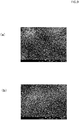
Figs. 2A and 2B are electron micrographs of sapphire members according to one or more embodiments, whereFig. 2A shows the sapphire member obtained through machining using a resin diamond plate as a polishing pad, and heating at 1950 °C for about 5 hours, followed by slow cooling, andFig. 2B shows the sapphire member obtained through the machining, and heating at 1950 °C for about 40 hours, followed by slow cooling. -
Figs. 3A and 3B are electron micrographs of sapphire members according to one or more embodiments, whereFig. 3A shows the sapphire member obtained through machining using a cast iron plate as a polishing pad, and heating at 1950 °C for about 5 hours, followed by slow cooling, andFig. 3B shows the sapphire member obtained through the machining, and heating at 1950 °C for about 40 hours, followed by slow cooling. -
Fig. 4 is a flowchart showing a method for manufacturing a sapphire member according to one or more embodiments. -
Fig. 5A is an electron micrograph of the sapphire member shown inFig. 2A or 2B during manufacture showing a main surface of its base material immediately after the machining, andFig. 5B is an electron micrograph of the sapphire member shown inFig. 3A or 3B during manufacture showing a main surface of its base material immediately after the machining. -
Fig. 6 is a diagram showing the crystal structure of a sapphire crystal. -
Figs. 7A and 7B are electron micrographs of sapphire members each showing a main surface substantially parallel to an m-plane immediately after the machining with another method for manufacturing a sapphire member according to one or more embodiments, whereFig. 7A shows the sapphire member obtained through machining using a resin diamond plate as a polishing pad, andFig. 7B shows the sapphire member obtained through machining using a cast iron plate as a polishing pad. -
Fig. 8A is a photograph of the base material for the sapphire member shown inFig. 7A cooled slowly after heated at 1950 °C for about 5 hours, andFig. 8B is a photograph of the base material for the sapphire member shownFig. 7A cooled slowly after heated at 1950 °C for about 40 hours. -
Figs. 9A is a photograph of the base material for the sapphire member shown inFig. 7B cooled slowly after heated at 1950 °C for about 5 hours, andFig. 9B is a photograph of the base material for the sapphire member shown inFig. 7B cooled slowly after heated at 1950 °C for about 40 hours. - In surface profile formation, roughening the surface of a sapphire member through mechanical polishing can easily form fine scratches or a damaged layer on the surface of a sapphire substrate, and also can cause polishing dust and other matter resulting from polishing to adhere to the surface. A sapphire substrate with a damaged layer or with polishing dust, when used as a GaN crystal growth substrate, can easily have the damaged layer or polishing dust broken or coming off, and thus may not grow a crystal layer, or a GaN layer, in a stable manner. For a sapphire member processed by reactive ion etching to form recesses and protrusions on the processed surface, the bottom surfaces of the recesses and the top surfaces of the protrusions are typically inclined with respect to the crystal face of sapphire. The processed surface is likely to be misaligned with the sapphire crystal face. A GaN crystal cannot form regularly on the surface misaligned with the sapphire crystal face. The surface processed by, for example, reactive ion etching can take a relatively long time for a crystal to grow to form a buffer layer with high surface crystallinity. The surface processed by reactive ion etching also uses other processes including a preceding photolithography process, and thus takes a relatively long time and large efforts. The resultant sapphire substrate can be relatively expensive.
- A sapphire substrate, which has high hardness to withstand damage, high light transmission, and high resistance to various chemicals, may be used in, for example, a storage tank for various chemical solutions. Such a storage tank formed by, for example, mechanical processing or grinding can have a disorderly roughened surface, and can scatter an excessively large amount of visible light at the main surface of the substrate and can reduce the light transmission of the sapphire substrate.
- A sapphire member according to the present embodiment and a method for manufacturing the sapphire member will now be described.
Fig. 1A is a schematic perspective view of asapphire member 1 according to the present embodiment.Fig. 1B is an enlarged sectional view of a portion of thesapphire member 1 including amain surface 1A.Fig. 1C is a further enlarged view of a portion of thesapphire member 1 including themain surface 1A. -
Figs. 2A, 2B ,3A, and 3B show examples of electron micrographs of thesapphire member 1. The electron micrographs shown in the drawings are all taken using the scanning electron microscope JSM-7001F (JEOL Ltd.). Thesapphire member 1 shown inFigs. 2A, 2B ,3A, and 3B is manufactured with a method for manufacturing a sapphire member according to one embodiment of the present invention. More specifically, thesapphire member 1 is manufactured through machining for preparing a base material having a main surface along the c-plane of a sapphire crystal, heating the base material to a temperature in a range of 1800 to 2000 °C, and slowly cooling the heated base material to room temperature in not less than six hours. The photographs shown inFigs. 2A, 2B ,3A, and 3B show thesapphire member 1 viewed in a plan in a direction perpendicular to themain surface 1A. - The
sapphire member 1 according to the present embodiment is mainly composed of sapphire, and has amain surface 1A along (substantially parallel to) the c-plane of the sapphire crystal. Thesapphire member 1 includes, in at least a part of itsmain surface 1A, a plurality of terrace structure layers 10 each having terrace surfaces 10α extending along (substantially parallel to) the c-plane of the sapphire crystal and side surfaces 10β in contact with anedge line 20 of the terrace surfaces 10α. In other words, specifically when thesapphire member 1 according to the present embodiment is viewed in a plan in a direction perpendicular to themain surface 1A, a plurality ofcurved edge lines 20 that are not parallel to one another (with varying intervals between the edge lines 20) are located in this surface part. - The
main surface 1A has appropriate recesses and protrusions in the part of themain surface 1A in which such terrace structure layers are located. Thesapphire member 1 used as, for example, a GaN crystal growth substrate allows an intended buffer layer to grow on thesapphire member 1 in a relatively short time. For example, a substrate called an off-angle substrate, which has a main surface inclined by a very small angle from the crystal face, such as the c-plane or α-plane, may have a step-terrace structure with a step height of about several tens to several hundreds of angstroms. This step-terrace structure has a plurality of straight ridgelines (ridgelines between a stepped portion and a terrace portion) extending parallel to one another in the direction corresponding to the direction of inclination. The off-angle substrate for forming an intended buffer layer within a relatively short time can have highly regularly arranged ridgelines and less surface irregularity. This structure causes large crystal grains to form locally at the initial stage of the crystal growth. Such crystal grains may disturb growth with entirely uniform crystal orientation, and delay formation of a sufficiently uniform buffer layer. - The
sapphire member 1 has a plurality ofcurved edge lines 20 that are not parallel to one another, which reduce local formation of large crystal grains. Thesapphire member 1 also has the terrace surfaces 10α along the c-plane of the sapphire crystal as described above. This structure allows the buffer layer having entirely uniform crystal orientation to grow, and allows an intended buffer layer to grow in a relatively short time. - The
sapphire member 1 used as a crystal growth substrate may haveterrace layer structures 10 across the entiremain surface 1A. Thesapphire member 1 may have a plurality ofcurved edge lines 20 that are not parallel to one another across the entiremain surface 1A. Theterrace layer structures 10 may be formed in at least a part of themain surface 1A, or the plurality ofterrace layer structures 10 may be formed in discrete parts of themain surface 1A. To grow, for example, an intended buffer layer in a relatively short time, a plurality ofterrace layer structures 10 may be located in an area larger than or equal to 50% of the area of themain surface 1A. - The
sapphire member 1 has a plurality of terrace surfaces 10α, each including aflat portion 30 larger than at least 1 µm square. More specifically, eachflat portion 30 larger than 1 µm square, which is equivalent to the wavelength of visible light, scatters less visible light. Thesapphire member 1 thus scatters a relatively small portion of the transmitted visible light. When, for example, used as a storage tank for various chemical solutions, thesapphire member 1, which scatters less light and is highly visible, allows easier visual inspection of the state of the chemical solution inside the storage tank from outside through thesapphire member 1. Theflat portions 30 of the terrace surfaces 10α are parallel to the c-plane of the sapphire crystal. Thus, thesapphire member 1 used as, for example, a GaN crystal growth substrate allows a GaN crystal with intended crystallinity to grow on the terrace surfaces 10α with a relatively large area. Thesapphire member 1 with this structure allows a buffer layer having an intended surface with less crystal defects and high crystallinity to grow on thesapphire member 1 in a relatively short time. - The
sapphire member 1 includes a plurality of terrace surfaces 10α, each including aflat portion 60 larger than at least 5 µm square. Theflat portion 60 larger than 5 µm square scatters less visible light than theflat portion 30, and increases the visibility of the light that transmits through thesapphire member 1. Theflat portions 60 of the terrace surfaces 10α facilitate growth of an intended GaN crystal and allow an intended buffer layer to grow on theflat portions 60 in a shorter time. - The
sapphire member 1 includes a plurality of closed-curve circle edges 21 viewed in a plan in a direction perpendicular to themain surface 1A. A first circle edge with a longer perimeter encloses a second circle edge with a shorter perimeter without crossing the second circle edge. More specifically, thesapphire member 1 includesprotrusions 40 each having a stepped surface and recesses 50 each having a stepped surface. Thesapphire member 1 with this structure prevents locally uniform crystal grains from growing on thesapphire member 1 during, for example, growth of a buffer layer, and allows a buffer layer with high crystallinity to grow on thesapphire member 1 in a relatively short time. - Each
protrusion 40 has a terrace surface 10α having the second circle edge with a shorter perimeter located above a terrace surface 10α having the first circle edge with a longer perimeter. Eachrecess 50 has a terrace surface 10α having the first circle edge with a longer perimeter located above a terrace surface 10α having the second circle edge with a shorter perimeter. Eachprotrusion 40 or eachrecess 50 has a plurality of terrace surfaces 10α. A buffer layer can also grow on the surfaces ofsuch protrusions 40 and recesses 50 to have relatively high crystallinity. - The GaN crystal or other crystal has a hexagonal crystal lattice. When circle edges 21 include at least one substantially
hexagonal circle edge 21, the substantiallyhexagonal circle edge 21 is aligned well with the growing GaN crystal. This structure also allows growth of the buffer layer with relatively high crystallinity. When each side of thehexagonal circle edge 21 extends along (substantially parallel to) the m-plane of the sapphire crystal, each side of the hexagon is substantially parallel to the corresponding side of thesapphire member 1, which serves as a growth substrate. Theprotrusions 40 and therecesses 50 are also aligned well with the GaN crystal, which grows with its crystal being aligned with the crystal of thesapphire member 1. This also allows growth of the buffer layer with relatively high crystallinity. -
Fig. 4 is a flowchart showing a method for manufacturing the sapphire member according to one or more embodiments of the present invention. The flowchart shown inFig. 4 also applies to the method for manufacturing thesapphire member 1 according to the present embodiment and also to other embodiments described later. - The method for manufacturing the
sapphire member 1 according to the present embodiment will now be described. For example, a sapphire-based plate is prepared first. The sapphire-based plate is formed from sapphire, which is a single crystal form of alumina grown by a crystal growth method, such as the edge-defined film-fed growth (EFG) method. The method for growing sapphire, which is a single crystal form of alumina, is not limited, and may be, for example, the Kyropoulos method or the heat exchanger method (HEM). - The method according to the present embodiment includes machining the sapphire-based plate to have, for example, an arithmetic mean roughness Ra of greater than or equal to 0.1 µm to obtain a base material having a main surface along the c-plane of a sapphire crystal, heating the base material to a temperature in a range of 1800 to 2000 °C, and slowly cooling the heated base material to room temperature in not less than six hours.
- Through the machining, the surface of the sapphire-based plate is ground with, for example, a surface grinder, which places a workpiece into slidable contact with the surface of a moving grindstone to mechanically grind the workpiece, to obtain a base material having a main surface substantially parallel to the c-plane of the sapphire crystal. The main surface processed with, for example, a surface grinder is the surface of sapphire having very high hardness ground by mechanical processing, and has an arithmetic mean roughness Ra of greater than or equal to 0.1 µm, which is relatively high (the surface is rough).
-
Figs. 5A and 5B are electron micrographs of the main surfaces of the base materials immediately after the machining.Fig. 5A shows the sapphire member machined with a surface grinder using a resin diamond plate as a polishing pad.Fig. 5B shows the sapphire member machined with a surface grinder using a cast iron plate as a polishing pad. More specifically,Fig. 5A shows the sapphire member polished (ground) with a surface grinder (Mitsui High-tec, Inc.) using a resin diamond plate #325 as a polishing plate in a 0.05-mm traverse mode.Fig. 5B shows the sapphire member polished with a lapping machine (Kyoritsu Seiki Corporation) using a cast iron plate as a polishing plate and diamond slurry with an average particle diameter of 25 µm in a self-weight mode. -
Fig. 5A is an electron micrograph of thesapphire member 1 shown inFigs. 2A and 2B during manufacture (photograph taken immediately after the machining).Fig. 5B is an electron micrograph of thesapphire member 1 shown inFigs. 3A and 3B during manufacture (photograph taken immediately after the machining). In the photographs shown inFigs. 5A and 5B , the mechanically ground sapphire, which is a single crystal form of alumina, is mechanically damaged to have a large number of fine cracks and breaks. For the workpiece immediately after the machining, for example, the light transmitted through the main surface is scattered at the cracks and breaks, and appears to be white and cloudy to an observer. - The method according to the present embodiment includes heating the machined base material (workpiece) to a temperature in a range of 1800 to 2000 °C, and then slowly cooling the heated base material to room temperature in not less than six hours. In the present embodiment, the machined base material is placed in a rare gas atmosphere in a furnace to undergo the heating and the slow cooling.
- In the heating process, the machined base material is first placed in the chamber of the furnace and the gas in the chamber is replaced with argon (Ar), which is a rare gas. Subsequently, the temperature inside the chamber is gradually raised to 1950 °C in about 14 hours and maintained at 1950 °C for about 5 to 50 hours. The melting point of sapphire is about 2070 °C. In the heating process, the temperature of the base material is raised to a temperature close to the melting point of sapphire and maintained at that temperature for a long time. Through the heating process, the outermost surface portion of the sapphire base material can, for example, partially melt to cause relaxation of atoms, and then causes reconstruction of the atoms.
- During this process, fine cracks and breaks on the surface of the sapphire created by mechanical damage through the machining seem to be fixed (or the gaps are closed). Also, the fine recesses and protrusions seem to be smoothed as the atoms are reconstructed to reduce the surface energy potential, or to reduce the surface area.
- After the heating process, the base material is cooled to room temperature in not less than six hours. Such gradual cooling in a long period of time facilitates crystallization of the outermost surface. In other words, the crystal portion mechanically damaged in the machining recrystallizes to correspond to the crystal portion underlying the damaged portion. Such slow cooling in a long period of time facilitates recrystallization and further smoothes the fine cracks and breaks on the damaged crystal portion.
-
Fig. 6 is a diagram showing the crystal structure of a sapphire crystal. As shown inFig. 6 , sapphire is a hexagonal system, which has a c-axis as a center axis, and a c-plane perpendicular to the c-axis, and six surfaces parallel to the c-axis, or the outer side surfaces of the hexagon, which are m-planes. Through the above machining and slow cooling, the terrace structure layers 10 having the terrace surfaces 10α, parallel to the c-plane of the sapphire crystal, and the side surfaces 10β, in contact with the terrace surfaces 10α, grow gradually. The main surface of the base material, which is substantially parallel to the c-plane of the sapphire crystal, allows a large crystal face to grow on the main surface in a direction parallel to the c-plane of the sapphire crystal. A large terrace surface 10α with a flat portion larger than at least 1 µm square can form on the main surface. The m-planes of the sapphire crystal, which are perpendicular to the c-plane of the sapphire crystal, also allow a crystal face to relatively easily form on the planes (allows crystal to be uniformly oriented). Thus, the side surfaces 10β perpendicular to the c-plane of the sapphire crystal also seem to facilitate crystal growth with a certain size to define aclear edge line 20. When the main surface is viewed in a plan in the direction perpendicular to the main surface, each terrace surface 10α hascurved edge lines 20 that are not parallel to one another and aflat portion 30 larger than at least 1 µm square. A plurality of terrace surfaces 10α are arranged to have a plurality ofedge lines 20 of a plurality of other stacked terrace structure layers 10. - The
sapphire member 1 can be manufactured through these processes.Figs. 2A and 2B show thesapphire members 1 machined using a diamond resin plate as a polishing pad.Fig. 2A shows thesapphire member 1 heated at 1950 °C for about 5 hours and then cooled slowly.Fig. 2B shows thesapphire member 1 heated at 1950 °C for about 40 hours and then cooled slowly.Figs. 3A to 3B show thesapphire members 1 machined using a cast iron plate as a polishing pad.Fig. 3A shows thesapphire member 1 heated at 1950 °C for about 5 hours and then cooled slowly.Fig. 3B shows thesapphire member 1 heated at 1950 °C for about 40 hours and then cooled slowly. As shown in the figures, thesapphire members 1 heated for a longer time (in the examples ofFigs. 2B and3B ) have larger terrace surfaces 10α than thesapphire members 1 heated for a shorter time (in the examples shown inFigs. 2A and3A ). Also as shown in the figures, thesapphire members 1 heated for a longer time havelarger protrusions 40 and recesses 50, and are shaped more similar to the hexagon. More specifically, thesapphire members 1 heated for a longer time have a greater growth on the m-planes. The dimensions or other characteristics of the terrace surfaces 10α, theprotrusions 40, and the recesses 50A can be regulated by adjusting the heating time. - The temperature used in the heating process may not be 1950 °C. The temperature may be higher than or equal to 1800 °C to form the terrace surface 10α with a relatively large size. The atmosphere in the furnace may not be limited. To form the terrace surface 10α with a relatively large size, the machined base material may be placed in a rare gas atmosphere, such as Ar, to undergo the heating and the slow cooling.
- The
sapphire member 1 manufactured with the manufacturing method according to the present embodiment may be used as, for example, a GaN crystal growth substrate. The manufacturing method according to the present embodiment can form thesapphire member 1 having an irregular surface substantially by simply placing the machined base material, which is to be thesapphire member 1, in a furnace, and eliminates photolithography or reactive ion etching after the machining. The manufacturing method according to the present embodiment can thus reduce the cost for manufacturing thesapphire member 1. The manufacturing method according to the present embodiment can also form thesapphire member 1 having a surface with a plurality ofcurved edge lines 20 that are not parallel to one another. Thissapphire member 1 allows, for example, a buffer layer having high crystallinity to form on thesapphire member 1 in a short time. The manufacturing method according to the present embodiment does not use chemical-mechanical polishing (CMP) and thus prevents excessive wear at the edges (or corner wear) of the main surface, which can often be caused by CMP. - A method for manufacturing a sapphire member according to another embodiment (second embodiment) will now be described. The same flowchart as shown in
Fig. 4 describes the method according to the second embodiment. The method according to the second embodiment includes machining the sapphire-based plate to have, for example, an arithmetic mean roughness Ra of greater than or equal to 0.1 µm to prepare a base material having a main surface along (substantially parallel to) an m-plane of a sapphire crystal, heating the base material to a temperature in a range of 1800 to 2000 °C, and slowly cooling the heated base material to room temperature in not less than six hours. The method according to the second embodiment differs from the method in the above embodiment in that an m-plane is used as the main surface of the base material obtained through the machining. The other processes according to the second embodiment use the same conditions as described in the above embodiment. - More specifically, the method according to the second embodiment may also use, for grinding the surface of the sapphire-based plate, a surface grinder that places a workpiece into slidable contact with the surface of a moving grindstone to mechanically grind the workpiece to prepare a base material having a main surface substantially parallel to the m-plane of the sapphire crystal. The machined main surface has an arithmetic mean roughness Ra of greater than or equal to 0.1 µm, which is relatively high (the surface is rough).
- Table 1 below shows the results of the experiments for determining the likelihood of particle formation on the sapphire member according to the first embodiment and another sapphire member. In Table 1, the sapphire member according to the first embodiment is the
sapphire member 1 shown inFig. 3A , or more specifically thesapphire member 1 machined using a cast iron plate as a polishing pad, heated at 1950 °C for about 5 hours, and then cooled slowly. In Table 1, the other sapphire is the sapphire member shown inFig. 5A , or more specifically the sapphire member without the heating and the slow cooling after its polishing process. Table 1 shows the particle count measured using a light-scattering liquid particle counter (or LPC). More specifically, test samples were placed in 5 L of pure water stored in a large beaker, and then underwent ultrasonic cleaning using ultrasonic waves applied through the pure water. The total number of particles having a diameter greater than or equal to 0.2 µm separated from each test sample into the pure water after the ultrasonic cleaning was then measured with LPC CLS-700T (Particle Measuring Systems, or PMS). Five such samples each for the first embodiment and for the other sapphire were prepared, and all the test samples were measured under the same conditions.Table 1 Sample Number First Embodiment Other Sapphire 1 172 1838 2 232 3072 3 258 4647 4 268 4722 5 276 4825 Average 241.2 3820.8 - As shown in Table 1, the samples according to the first embodiment have significantly fewer generated particles. This is seemingly because the fine cracks and breaks generated by the crystal portion damaged by polishing have been fixed by recrystallization through heating and slow cooling.
-
Figs. 7A and 7B are electron micrographs each showing the main surface substantially parallel to an m-plane immediately after the machining in the second embodiment.Fig. 7A shows the sapphire member machined with a surface grinder using a resin diamond plate as a polishing pad.Fig. 7B shows the sapphire member machined with a surface grinder using a cast iron plate as a polishing pad. In the photographs shown inFigs. 7A and 7B , the mechanically ground sapphire, which is a single crystal form of alumina, is mechanically damaged to have a large number of fine cracks and breaks. - The machining is then followed by heating the machined base material (workpiece) to a temperature in a range of 1800 to 2000 °C, and then slowly cooling the heated base material to room temperature in not less than six hours. In the second embodiment as well, the machined base material is placed in a rare gas atmosphere in a furnace to undergo the heating and the slow cooling.
- In the heating process, the machined base material is first placed in the chamber of the furnace, and the gas in the chamber is replaced with Ar, which is a rare gas. Subsequently, the temperature inside the chamber is gradually raised to 1950 °C in about 14 hours and maintained at 1950 °C for about 5 to 50 hours. After the heating process, the base material is cooled to room temperature in not less than six hours. Such gradual cooling in a long period of time facilitates crystallization of the outermost surface.
-
Figs. 8A, 8B ,9A, and 9B are electron micrographs each showing the main surface parallel to the m-plane of a sapphire crystal that has undergone the slow cooling.Figs. 8A and 8B are the photographs of the base material shown inFig. 7A taken after the heating and the slow cooling.Fig. 8A shows the base material heated at 1950 °C for about 5 hours and then cooled slowly.Fig. 8B shows the base material heated at 1950 °C for about 40 hours and then cooled slowly.Figs. 9A and 9B are the photographs each showing the base material shown inFig. 7B taken after the heating and the slow cooling.Figs. 9A shows the base material heated at 1950 °C for about 5 hours and then cooled slowly.Fig. 9B shows the base material heated at 1950 °C for about 40 hours and then cooled slowly. - Also in the second embodiment, the portion of the crystal mechanically damaged in the machining recrystallizes to correspond to the crystal portion underlying the damaged portion. Such slow cooling facilitates recrystallization and further smoothes fine cracks and breaks on the damaged crystal portion. The electron micrographs in the second embodiment show the surface parallel to the m-plane with significantly fewer recesses and protrusions and with no perceivable boundary between the crystal layers, or with no
edge lines 20 for example. This is seemingly because the m-plane of the sapphire crystal layer is uniformly oriented more easily than other crystal layers, such as the c-plane of the sapphire crystal. - The photographs in
Figs. 8A, 8B ,9A, and 9B reveal that the heating at the predetermined temperature for about five hours can sufficiently smooth the surface, and increasing the heating time to about 40 hours does not greatly change the states of the recesses and protrusions on the surface. For example, the sapphire member shown inFig. 8A has an arithmetic mean roughness Ra of 0.25 µm, and has a main surface precisely smoothed with the manufacturing method according to the second embodiment. - The manufacturing method according to the second embodiment yields a sapphire member having a relatively flat main surface parallel to the m-plane at low cost with a relatively short time and small efforts. Sapphire, which has high hardness, is usually smoothed precisely by polishing the ground main surface of the sapphire member a plurality of times in a stepwise manner, and finally polishing the main surface by chemical mechanical polishing (CMP) using colloidal silica to have, for example, an arithmetic mean roughness Ra of lower than 0.5 µm. This smoothing process through polishing alone uses different types of large polishing machines, and takes time, ranging from half a day to several days, for the polishing operations, as well as efforts, such as frequent checks during polishing operations. The second embodiment allows the machining including polishing to be followed substantially simply by placing the sapphire member in the furnace, in which both the heating and the slow cooling are performed. This eliminates large efforts. The surface can be smoothed through a single heating process and a single slow cooling process. This shortens the total operation time. The method for manufacturing a sapphire member according to the second embodiment of the present invention thus yields a sapphire member that scatters a small portion of the transmitted light at relatively low cost. The method according to the second embodiment can also form a sapphire member having a high-precision smooth surface without CMP, and thus prevents excessive wear at the edges (or corner wear) of the main surface, which can be easily caused by polishing such as CMP.
- Also in the second embodiment, the temperature used in the heating process may not be 1950 °C but may be higher than or equal to 1800 °C to provide a high-precision smooth surface. The atmosphere in the furnace may not be limited. To smooth the surface with high precision, the machined base material may be placed in a rare gas atmosphere, such as Ar to undergo the heating and the slow cooling.
- Through trial-and-error experiments, the inventors of the present application have been the first to notice the difference between the surface structures with different crystal orientations of a sapphire-based member after machined at the temperature close to the melting point of sapphire, and the detailed structures.
- Although the embodiments or examples of the present invention have been described above, the present invention is not limited to the above embodiments or examples. The present invention may be modified or changed in various manners without departing from the spirit and scope of the present invention.
-
- 1
- sapphire member
- 1A
- main surface
- 10
- terrace structure layer
- 10α
- terrace surface
- 10β
- side surface
- 20
- edge line
- 21
- circle edge
- 30, 60
- flat portion
- 40
- protrusion
- 50
- recess
Claims (10)
- A sapphire member comprising sapphire as a main constituent and having a main surface along a c-plane of a sapphire crystal, the sapphire member comprising:a plurality of terrace structure layers in at least a part of the main surface, each terrace structure layer including a terrace surface along the c-plane and a side surface in contact with an edge line of the terrace surface.
- The sapphire member according to claim 1, wherein
the terrace surface includes a flat portion larger than 1 µm square. - The sapphire member according to claim 2, wherein
the terrace surface includes a flat portion larger than 5 µm square. - The sapphire member according to any one of claims 1 to 3, wherein
the main surface includes, as viewed in a plan, circle edges of a closed curve including a first circle edge having a longer perimeter and a second circle edge having a shorter perimeter, and the first circle edge encloses the second circle edge without crossing the second circle edge. - The sapphire member according to claim 4, wherein
the second circle edge is located above the first circle edge. - The sapphire member according to claim 4, wherein
the first circle edge is located above the second circle edge. - The sapphire member according to any one of claims 4 to 6, wherein
at least one of the circle edges is a hexagonal circle edge. - The sapphire member according to claim 7, wherein
the hexagonal circle edge has sides each extending along an m-plane of the sapphire crystal. - A method for manufacturing the sapphire member according to any one of claims 1 to 8, the method comprising:preparing a base material having a main surface along the c-plane of the sapphire crystal;heating the base material to a temperature in a range of 1800 to 2000 °C; andslowly cooling the heated base material to room temperature in not less than six hours.
- A method for manufacturing a sapphire member, comprising:preparing a base material having a main surface along an m-plane of a sapphire crystal;heating the base material to a temperature in a range of 1800 to 2000 °C; andslowly cooling the heated base material to room temperature in not less than six hours.
Applications Claiming Priority (2)
| Application Number | Priority Date | Filing Date | Title |
|---|---|---|---|
| JP2015063735 | 2015-03-26 | ||
| PCT/JP2016/059900 WO2016153070A1 (en) | 2015-03-26 | 2016-03-28 | Sapphire member and method for manufacturing sapphire member |
Publications (3)
| Publication Number | Publication Date |
|---|---|
| EP3276049A1 true EP3276049A1 (en) | 2018-01-31 |
| EP3276049A4 EP3276049A4 (en) | 2018-12-05 |
| EP3276049B1 EP3276049B1 (en) | 2021-03-24 |
Family
ID=56978981
Family Applications (1)
| Application Number | Title | Priority Date | Filing Date |
|---|---|---|---|
| EP16768972.8A Active EP3276049B1 (en) | 2015-03-26 | 2016-03-28 | Sapphire member and method for manufacturing sapphire member |
Country Status (5)
| Country | Link |
|---|---|
| US (1) | US10351969B2 (en) |
| EP (1) | EP3276049B1 (en) |
| JP (1) | JP6633615B2 (en) |
| CN (1) | CN107407006B (en) |
| WO (1) | WO2016153070A1 (en) |
Cited By (3)
| Publication number | Priority date | Publication date | Assignee | Title |
|---|---|---|---|---|
| EP3564728A4 (en) * | 2016-12-28 | 2020-09-09 | Kyocera Corporation | EXTERIOR IMAGE RADIATION DEVICE |
| EP3805631A4 (en) * | 2018-05-24 | 2022-03-23 | Kyocera Corporation | OPTICAL DEVICE |
| EP3805630A4 (en) * | 2018-05-24 | 2022-03-23 | Kyocera Corporation | Optical device |
Families Citing this family (3)
| Publication number | Priority date | Publication date | Assignee | Title |
|---|---|---|---|---|
| JP6851017B2 (en) * | 2016-05-18 | 2021-03-31 | パナソニックIpマネジメント株式会社 | Device and its manufacturing method |
| JP6741777B2 (en) * | 2016-11-02 | 2020-08-19 | 京セラ株式会社 | Color wheel substrate, color wheel and projector, and method for manufacturing color wheel substrate |
| EP3805629B1 (en) * | 2018-05-24 | 2024-04-17 | Kyocera Corporation | Optical device |
Family Cites Families (29)
| Publication number | Priority date | Publication date | Assignee | Title |
|---|---|---|---|---|
| US5422306A (en) * | 1991-12-17 | 1995-06-06 | Matsushita Electric Industrial Co., Ltd. | Method of forming semiconductor hetero interfaces |
| US6083812A (en) * | 1993-02-02 | 2000-07-04 | Texas Instruments Incorporated | Heteroepitaxy by large surface steps |
| CA2258080C (en) * | 1997-04-11 | 2007-06-05 | Nichia Chemical Industries, Ltd. | Nitride semiconductor growth method, nitride semiconductor substrate, and nitride semiconductor device |
| US6091085A (en) | 1998-02-19 | 2000-07-18 | Agilent Technologies, Inc. | GaN LEDs with improved output coupling efficiency |
| US6180497B1 (en) * | 1998-07-23 | 2001-01-30 | Canon Kabushiki Kaisha | Method for producing semiconductor base members |
| JP3929008B2 (en) * | 2000-01-14 | 2007-06-13 | シャープ株式会社 | Nitride-based compound semiconductor light-emitting device and method for manufacturing the same |
| CH696907A5 (en) * | 2003-02-18 | 2008-01-31 | Schott Ag | A process for the manufacture of hexagonal monocrystals and their use as a substrate for semiconductor devices. |
| KR100679737B1 (en) * | 2003-05-19 | 2007-02-07 | 도시바세라믹스가부시키가이샤 | Manufacturing Method of Silicon Substrate Having Distortion Layer |
| JP2006062931A (en) * | 2004-08-30 | 2006-03-09 | Kyocera Corp | Sapphire substrate, heat treatment method thereof, and crystal growth method |
| JP4742360B2 (en) * | 2005-05-26 | 2011-08-10 | 並木精密宝石株式会社 | Method for arranging micro holes in an array, AFM standard sample, and AFM stage |
| CN1743514A (en) * | 2005-08-11 | 2006-03-08 | 周永宗 | Annealing treatment method of crystal in neutral and inert atmosphere |
| JP5129740B2 (en) * | 2006-04-17 | 2013-01-30 | 株式会社 斉藤光学製作所 | Single crystal sapphire substrate |
| JP2008031027A (en) * | 2006-06-28 | 2008-02-14 | Namiki Precision Jewel Co Ltd | Sapphire single crystal substrate |
| KR101172942B1 (en) * | 2006-10-20 | 2012-08-14 | 도꾸리쯔교세이호징 리가가쿠 겐큐소 | Sapphire substrate, nitride semiconductor luminescent element using the sapphire substrate, and method for manufacturing the nitride semiconductor luminescent element |
| JP5145488B2 (en) * | 2007-04-02 | 2013-02-20 | 住友金属鉱山株式会社 | Sapphire single crystal substrate and manufacturing method thereof |
| TW201130156A (en) * | 2009-11-26 | 2011-09-01 | Showa Denko Kk | Sapphire single crystal for producing sapphire single crystal substrate for LED, sapphire single crystal substrate for LED, light-eliciting element, and method for preparing the same |
| JP2010168280A (en) * | 2010-03-08 | 2010-08-05 | Kyocera Corp | Single crystal sapphire substrate |
| US8110484B1 (en) * | 2010-11-19 | 2012-02-07 | Sumitomo Electric Industries, Ltd. | Conductive nitride semiconductor substrate and method for producing the same |
| CN102634850A (en) * | 2012-03-31 | 2012-08-15 | 江苏鑫和泰光电科技有限公司 | Annealing method of sapphire wafer |
| CN202595343U (en) * | 2012-04-01 | 2012-12-12 | 江苏鑫和泰光电科技有限公司 | Sapphire substrate annealing furnace |
| CN102769082B (en) * | 2012-07-02 | 2015-04-29 | 杭州士兰明芯科技有限公司 | Patterned substrate, method for forming same, and mask plate used for making said substrate |
| KR101439380B1 (en) * | 2012-10-31 | 2014-09-11 | 주식회사 사파이어테크놀로지 | Heat Treatment Method and Apparatus for Sapphier Single Crystal |
| CN203007496U (en) * | 2012-12-29 | 2013-06-19 | 青岛嘉星晶电科技股份有限公司 | Sapphire annealing tool |
| CN103014874A (en) * | 2013-01-11 | 2013-04-03 | 焦作市光源晶电科技有限公司 | Sapphire crystal annealing process |
| CN103540998A (en) * | 2013-08-20 | 2014-01-29 | 曾锡强 | Annealing process for growing large-size sapphire crystal by kyropoulos method |
| CN103643300B (en) * | 2013-11-26 | 2017-04-12 | 浙江上城科技有限公司 | Annealing method applied to sapphire processing |
| CN104088014B (en) * | 2014-07-11 | 2016-08-17 | 江苏中电振华晶体技术有限公司 | A kind of bar-shaped sapphire crystal growth equipment and growing method thereof |
| JP2016044099A (en) * | 2014-08-22 | 2016-04-04 | 住友金属鉱山株式会社 | Aluminum oxide single crystal wafer manufacturing method and aluminum oxide single crystal wafer |
| JP2016047784A (en) * | 2014-08-27 | 2016-04-07 | 住友金属鉱山株式会社 | Method for producing aluminum oxide single crystal wafer |
-
2016
- 2016-03-28 EP EP16768972.8A patent/EP3276049B1/en active Active
- 2016-03-28 JP JP2017507648A patent/JP6633615B2/en active Active
- 2016-03-28 CN CN201680018288.2A patent/CN107407006B/en active Active
- 2016-03-28 US US15/561,849 patent/US10351969B2/en active Active
- 2016-03-28 WO PCT/JP2016/059900 patent/WO2016153070A1/en not_active Ceased
Cited By (3)
| Publication number | Priority date | Publication date | Assignee | Title |
|---|---|---|---|---|
| EP3564728A4 (en) * | 2016-12-28 | 2020-09-09 | Kyocera Corporation | EXTERIOR IMAGE RADIATION DEVICE |
| EP3805631A4 (en) * | 2018-05-24 | 2022-03-23 | Kyocera Corporation | OPTICAL DEVICE |
| EP3805630A4 (en) * | 2018-05-24 | 2022-03-23 | Kyocera Corporation | Optical device |
Also Published As
| Publication number | Publication date |
|---|---|
| US10351969B2 (en) | 2019-07-16 |
| CN107407006B (en) | 2020-09-01 |
| US20180112332A1 (en) | 2018-04-26 |
| EP3276049A4 (en) | 2018-12-05 |
| JPWO2016153070A1 (en) | 2017-12-21 |
| WO2016153070A1 (en) | 2016-09-29 |
| CN107407006A (en) | 2017-11-28 |
| EP3276049B1 (en) | 2021-03-24 |
| JP6633615B2 (en) | 2020-01-22 |
Similar Documents
| Publication | Publication Date | Title |
|---|---|---|
| EP3276049B1 (en) | Sapphire member and method for manufacturing sapphire member | |
| RU2412037C1 (en) | Lot of sapphire substrates and method of its production | |
| EP2121242B1 (en) | Method of grinding a sapphire substrate | |
| EP2671975B1 (en) | Sapphire substrates | |
| KR102654261B1 (en) | Ga2O3-BASED SINGLE CRYSTAL SUBSTRATE | |
| TWI494981B (en) | Modified microgrinding process | |
| CN101743092B (en) | Method for Crystal Reorientation of Single Crystal | |
| US8740670B2 (en) | Sapphire substrates and methods of making same | |
| KR20060017676A (en) | Method for Manufacturing Silicon Wafer, Silicon Wafer and SOI Wafer | |
| JP7650958B2 (en) | AlN single crystal substrate | |
| US10246796B2 (en) | RAMO4 substrate | |
| WO2015172014A1 (en) | High quality sapphire substrates and method of making said sapphire substrates | |
| CN107099844A (en) | RAMO4Substrate and its manufacture method | |
| JP4539053B2 (en) | Single crystal substrate and manufacturing method thereof | |
| CN107119320A (en) | RAMO4 substrates and its manufacture method |
Legal Events
| Date | Code | Title | Description |
|---|---|---|---|
| STAA | Information on the status of an ep patent application or granted ep patent |
Free format text: STATUS: THE INTERNATIONAL PUBLICATION HAS BEEN MADE |
|
| PUAI | Public reference made under article 153(3) epc to a published international application that has entered the european phase |
Free format text: ORIGINAL CODE: 0009012 |
|
| STAA | Information on the status of an ep patent application or granted ep patent |
Free format text: STATUS: REQUEST FOR EXAMINATION WAS MADE |
|
| 17P | Request for examination filed |
Effective date: 20170925 |
|
| AK | Designated contracting states |
Kind code of ref document: A1 Designated state(s): AL AT BE BG CH CY CZ DE DK EE ES FI FR GB GR HR HU IE IS IT LI LT LU LV MC MK MT NL NO PL PT RO RS SE SI SK SM TR |
|
| AX | Request for extension of the european patent |
Extension state: BA ME |
|
| DAV | Request for validation of the european patent (deleted) | ||
| DAX | Request for extension of the european patent (deleted) | ||
| A4 | Supplementary search report drawn up and despatched |
Effective date: 20181030 |
|
| RIC1 | Information provided on ipc code assigned before grant |
Ipc: C30B 33/02 20060101ALI20181024BHEP Ipc: C30B 29/20 20060101AFI20181024BHEP |
|
| STAA | Information on the status of an ep patent application or granted ep patent |
Free format text: STATUS: EXAMINATION IS IN PROGRESS |
|
| 17Q | First examination report despatched |
Effective date: 20200305 |
|
| GRAP | Despatch of communication of intention to grant a patent |
Free format text: ORIGINAL CODE: EPIDOSNIGR1 |
|
| STAA | Information on the status of an ep patent application or granted ep patent |
Free format text: STATUS: GRANT OF PATENT IS INTENDED |
|
| INTG | Intention to grant announced |
Effective date: 20201105 |
|
| GRAS | Grant fee paid |
Free format text: ORIGINAL CODE: EPIDOSNIGR3 |
|
| GRAA | (expected) grant |
Free format text: ORIGINAL CODE: 0009210 |
|
| STAA | Information on the status of an ep patent application or granted ep patent |
Free format text: STATUS: THE PATENT HAS BEEN GRANTED |
|
| AK | Designated contracting states |
Kind code of ref document: B1 Designated state(s): AL AT BE BG CH CY CZ DE DK EE ES FI FR GB GR HR HU IE IS IT LI LT LU LV MC MK MT NL NO PL PT RO RS SE SI SK SM TR |
|
| REG | Reference to a national code |
Ref country code: GB Ref legal event code: FG4D |
|
| REG | Reference to a national code |
Ref country code: CH Ref legal event code: EP |
|
| REG | Reference to a national code |
Ref country code: IE Ref legal event code: FG4D |
|
| REG | Reference to a national code |
Ref country code: AT Ref legal event code: REF Ref document number: 1374611 Country of ref document: AT Kind code of ref document: T Effective date: 20210415 Ref country code: DE Ref legal event code: R096 Ref document number: 602016054862 Country of ref document: DE |
|
| REG | Reference to a national code |
Ref country code: LT Ref legal event code: MG9D |
|
| PG25 | Lapsed in a contracting state [announced via postgrant information from national office to epo] |
Ref country code: HR Free format text: LAPSE BECAUSE OF FAILURE TO SUBMIT A TRANSLATION OF THE DESCRIPTION OR TO PAY THE FEE WITHIN THE PRESCRIBED TIME-LIMIT Effective date: 20210324 Ref country code: GR Free format text: LAPSE BECAUSE OF FAILURE TO SUBMIT A TRANSLATION OF THE DESCRIPTION OR TO PAY THE FEE WITHIN THE PRESCRIBED TIME-LIMIT Effective date: 20210625 Ref country code: FI Free format text: LAPSE BECAUSE OF FAILURE TO SUBMIT A TRANSLATION OF THE DESCRIPTION OR TO PAY THE FEE WITHIN THE PRESCRIBED TIME-LIMIT Effective date: 20210324 Ref country code: NO Free format text: LAPSE BECAUSE OF FAILURE TO SUBMIT A TRANSLATION OF THE DESCRIPTION OR TO PAY THE FEE WITHIN THE PRESCRIBED TIME-LIMIT Effective date: 20210624 Ref country code: BG Free format text: LAPSE BECAUSE OF FAILURE TO SUBMIT A TRANSLATION OF THE DESCRIPTION OR TO PAY THE FEE WITHIN THE PRESCRIBED TIME-LIMIT Effective date: 20210624 |
|
| PG25 | Lapsed in a contracting state [announced via postgrant information from national office to epo] |
Ref country code: SE Free format text: LAPSE BECAUSE OF FAILURE TO SUBMIT A TRANSLATION OF THE DESCRIPTION OR TO PAY THE FEE WITHIN THE PRESCRIBED TIME-LIMIT Effective date: 20210324 Ref country code: RS Free format text: LAPSE BECAUSE OF FAILURE TO SUBMIT A TRANSLATION OF THE DESCRIPTION OR TO PAY THE FEE WITHIN THE PRESCRIBED TIME-LIMIT Effective date: 20210324 Ref country code: LV Free format text: LAPSE BECAUSE OF FAILURE TO SUBMIT A TRANSLATION OF THE DESCRIPTION OR TO PAY THE FEE WITHIN THE PRESCRIBED TIME-LIMIT Effective date: 20210324 |
|
| REG | Reference to a national code |
Ref country code: NL Ref legal event code: MP Effective date: 20210324 |
|
| REG | Reference to a national code |
Ref country code: AT Ref legal event code: MK05 Ref document number: 1374611 Country of ref document: AT Kind code of ref document: T Effective date: 20210324 |
|
| PG25 | Lapsed in a contracting state [announced via postgrant information from national office to epo] |
Ref country code: NL Free format text: LAPSE BECAUSE OF FAILURE TO SUBMIT A TRANSLATION OF THE DESCRIPTION OR TO PAY THE FEE WITHIN THE PRESCRIBED TIME-LIMIT Effective date: 20210324 |
|
| PG25 | Lapsed in a contracting state [announced via postgrant information from national office to epo] |
Ref country code: CZ Free format text: LAPSE BECAUSE OF FAILURE TO SUBMIT A TRANSLATION OF THE DESCRIPTION OR TO PAY THE FEE WITHIN THE PRESCRIBED TIME-LIMIT Effective date: 20210324 Ref country code: EE Free format text: LAPSE BECAUSE OF FAILURE TO SUBMIT A TRANSLATION OF THE DESCRIPTION OR TO PAY THE FEE WITHIN THE PRESCRIBED TIME-LIMIT Effective date: 20210324 Ref country code: LT Free format text: LAPSE BECAUSE OF FAILURE TO SUBMIT A TRANSLATION OF THE DESCRIPTION OR TO PAY THE FEE WITHIN THE PRESCRIBED TIME-LIMIT Effective date: 20210324 Ref country code: AT Free format text: LAPSE BECAUSE OF FAILURE TO SUBMIT A TRANSLATION OF THE DESCRIPTION OR TO PAY THE FEE WITHIN THE PRESCRIBED TIME-LIMIT Effective date: 20210324 Ref country code: SM Free format text: LAPSE BECAUSE OF FAILURE TO SUBMIT A TRANSLATION OF THE DESCRIPTION OR TO PAY THE FEE WITHIN THE PRESCRIBED TIME-LIMIT Effective date: 20210324 |
|
| REG | Reference to a national code |
Ref country code: CH Ref legal event code: PL |
|
| PG25 | Lapsed in a contracting state [announced via postgrant information from national office to epo] |
Ref country code: IS Free format text: LAPSE BECAUSE OF FAILURE TO SUBMIT A TRANSLATION OF THE DESCRIPTION OR TO PAY THE FEE WITHIN THE PRESCRIBED TIME-LIMIT Effective date: 20210724 Ref country code: PT Free format text: LAPSE BECAUSE OF FAILURE TO SUBMIT A TRANSLATION OF THE DESCRIPTION OR TO PAY THE FEE WITHIN THE PRESCRIBED TIME-LIMIT Effective date: 20210726 Ref country code: PL Free format text: LAPSE BECAUSE OF FAILURE TO SUBMIT A TRANSLATION OF THE DESCRIPTION OR TO PAY THE FEE WITHIN THE PRESCRIBED TIME-LIMIT Effective date: 20210324 Ref country code: SK Free format text: LAPSE BECAUSE OF FAILURE TO SUBMIT A TRANSLATION OF THE DESCRIPTION OR TO PAY THE FEE WITHIN THE PRESCRIBED TIME-LIMIT Effective date: 20210324 Ref country code: RO Free format text: LAPSE BECAUSE OF FAILURE TO SUBMIT A TRANSLATION OF THE DESCRIPTION OR TO PAY THE FEE WITHIN THE PRESCRIBED TIME-LIMIT Effective date: 20210324 |
|
| REG | Reference to a national code |
Ref country code: BE Ref legal event code: MM Effective date: 20210331 |
|
| REG | Reference to a national code |
Ref country code: DE Ref legal event code: R097 Ref document number: 602016054862 Country of ref document: DE |
|
| PG25 | Lapsed in a contracting state [announced via postgrant information from national office to epo] |
Ref country code: DK Free format text: LAPSE BECAUSE OF FAILURE TO SUBMIT A TRANSLATION OF THE DESCRIPTION OR TO PAY THE FEE WITHIN THE PRESCRIBED TIME-LIMIT Effective date: 20210324 Ref country code: ES Free format text: LAPSE BECAUSE OF FAILURE TO SUBMIT A TRANSLATION OF THE DESCRIPTION OR TO PAY THE FEE WITHIN THE PRESCRIBED TIME-LIMIT Effective date: 20210324 Ref country code: IE Free format text: LAPSE BECAUSE OF NON-PAYMENT OF DUE FEES Effective date: 20210328 Ref country code: CH Free format text: LAPSE BECAUSE OF NON-PAYMENT OF DUE FEES Effective date: 20210331 Ref country code: AL Free format text: LAPSE BECAUSE OF FAILURE TO SUBMIT A TRANSLATION OF THE DESCRIPTION OR TO PAY THE FEE WITHIN THE PRESCRIBED TIME-LIMIT Effective date: 20210324 Ref country code: MC Free format text: LAPSE BECAUSE OF FAILURE TO SUBMIT A TRANSLATION OF THE DESCRIPTION OR TO PAY THE FEE WITHIN THE PRESCRIBED TIME-LIMIT Effective date: 20210324 Ref country code: LI Free format text: LAPSE BECAUSE OF NON-PAYMENT OF DUE FEES Effective date: 20210331 Ref country code: LU Free format text: LAPSE BECAUSE OF NON-PAYMENT OF DUE FEES Effective date: 20210328 |
|
| PLBE | No opposition filed within time limit |
Free format text: ORIGINAL CODE: 0009261 |
|
| STAA | Information on the status of an ep patent application or granted ep patent |
Free format text: STATUS: NO OPPOSITION FILED WITHIN TIME LIMIT |
|
| PG25 | Lapsed in a contracting state [announced via postgrant information from national office to epo] |
Ref country code: SI Free format text: LAPSE BECAUSE OF FAILURE TO SUBMIT A TRANSLATION OF THE DESCRIPTION OR TO PAY THE FEE WITHIN THE PRESCRIBED TIME-LIMIT Effective date: 20210324 |
|
| 26N | No opposition filed |
Effective date: 20220104 |
|
| PG25 | Lapsed in a contracting state [announced via postgrant information from national office to epo] |
Ref country code: IS Free format text: LAPSE BECAUSE OF FAILURE TO SUBMIT A TRANSLATION OF THE DESCRIPTION OR TO PAY THE FEE WITHIN THE PRESCRIBED TIME-LIMIT Effective date: 20210724 Ref country code: FR Free format text: LAPSE BECAUSE OF NON-PAYMENT OF DUE FEES Effective date: 20210524 |
|
| PG25 | Lapsed in a contracting state [announced via postgrant information from national office to epo] |
Ref country code: BE Free format text: LAPSE BECAUSE OF NON-PAYMENT OF DUE FEES Effective date: 20210331 |
|
| PG25 | Lapsed in a contracting state [announced via postgrant information from national office to epo] |
Ref country code: IT Free format text: LAPSE BECAUSE OF FAILURE TO SUBMIT A TRANSLATION OF THE DESCRIPTION OR TO PAY THE FEE WITHIN THE PRESCRIBED TIME-LIMIT Effective date: 20210324 |
|
| P01 | Opt-out of the competence of the unified patent court (upc) registered |
Effective date: 20230505 |
|
| PG25 | Lapsed in a contracting state [announced via postgrant information from national office to epo] |
Ref country code: CY Free format text: LAPSE BECAUSE OF FAILURE TO SUBMIT A TRANSLATION OF THE DESCRIPTION OR TO PAY THE FEE WITHIN THE PRESCRIBED TIME-LIMIT Effective date: 20210324 |
|
| PG25 | Lapsed in a contracting state [announced via postgrant information from national office to epo] |
Ref country code: HU Free format text: LAPSE BECAUSE OF FAILURE TO SUBMIT A TRANSLATION OF THE DESCRIPTION OR TO PAY THE FEE WITHIN THE PRESCRIBED TIME-LIMIT; INVALID AB INITIO Effective date: 20160328 |
|
| PG25 | Lapsed in a contracting state [announced via postgrant information from national office to epo] |
Ref country code: MK Free format text: LAPSE BECAUSE OF FAILURE TO SUBMIT A TRANSLATION OF THE DESCRIPTION OR TO PAY THE FEE WITHIN THE PRESCRIBED TIME-LIMIT Effective date: 20210324 |
|
| PG25 | Lapsed in a contracting state [announced via postgrant information from national office to epo] |
Ref country code: TR Free format text: LAPSE BECAUSE OF FAILURE TO SUBMIT A TRANSLATION OF THE DESCRIPTION OR TO PAY THE FEE WITHIN THE PRESCRIBED TIME-LIMIT Effective date: 20210324 |
|
| PG25 | Lapsed in a contracting state [announced via postgrant information from national office to epo] |
Ref country code: MT Free format text: LAPSE BECAUSE OF FAILURE TO SUBMIT A TRANSLATION OF THE DESCRIPTION OR TO PAY THE FEE WITHIN THE PRESCRIBED TIME-LIMIT Effective date: 20210324 |
|
| PGFP | Annual fee paid to national office [announced via postgrant information from national office to epo] |
Ref country code: GB Payment date: 20250206 Year of fee payment: 10 |
|
| PGFP | Annual fee paid to national office [announced via postgrant information from national office to epo] |
Ref country code: DE Payment date: 20260204 Year of fee payment: 11 |