EP3274728B1 - Multi-input scalable rectifier droop detector - Google Patents
Multi-input scalable rectifier droop detector Download PDFInfo
- Publication number
- EP3274728B1 EP3274728B1 EP16715947.4A EP16715947A EP3274728B1 EP 3274728 B1 EP3274728 B1 EP 3274728B1 EP 16715947 A EP16715947 A EP 16715947A EP 3274728 B1 EP3274728 B1 EP 3274728B1
- Authority
- EP
- European Patent Office
- Prior art keywords
- droop
- detector
- input
- output
- detecting
- Prior art date
- Legal status (The legal status is an assumption and is not a legal conclusion. Google has not performed a legal analysis and makes no representation as to the accuracy of the status listed.)
- Active
Links
Images


Classifications
-
- H—ELECTRICITY
- H02—GENERATION; CONVERSION OR DISTRIBUTION OF ELECTRIC POWER
- H02M—APPARATUS FOR CONVERSION BETWEEN AC AND AC, BETWEEN AC AND DC, OR BETWEEN DC AND DC, AND FOR USE WITH MAINS OR SIMILAR POWER SUPPLY SYSTEMS; CONVERSION OF DC OR AC INPUT POWER INTO SURGE OUTPUT POWER; CONTROL OR REGULATION THEREOF
- H02M7/00—Conversion of AC power input into DC power output; Conversion of DC power input into AC power output
- H02M7/02—Conversion of AC power input into DC power output without possibility of reversal
- H02M7/04—Conversion of AC power input into DC power output without possibility of reversal by static converters
- H02M7/12—Conversion of AC power input into DC power output without possibility of reversal by static converters using discharge tubes with control electrode or semiconductor devices with control electrode
- H02M7/21—Conversion of AC power input into DC power output without possibility of reversal by static converters using discharge tubes with control electrode or semiconductor devices with control electrode using devices of a triode or transistor type requiring continuous application of a control signal
- H02M7/217—Conversion of AC power input into DC power output without possibility of reversal by static converters using discharge tubes with control electrode or semiconductor devices with control electrode using devices of a triode or transistor type requiring continuous application of a control signal using semiconductor devices only
-
- G—PHYSICS
- G01—MEASURING; TESTING
- G01R—MEASURING ELECTRIC VARIABLES; MEASURING MAGNETIC VARIABLES
- G01R19/00—Arrangements for measuring currents or voltages or for indicating presence or sign thereof
- G01R19/0084—Arrangements for measuring currents or voltages or for indicating presence or sign thereof measuring voltage only
-
- G—PHYSICS
- G01—MEASURING; TESTING
- G01R—MEASURING ELECTRIC VARIABLES; MEASURING MAGNETIC VARIABLES
- G01R19/00—Arrangements for measuring currents or voltages or for indicating presence or sign thereof
- G01R19/165—Indicating that current or voltage is either above or below a predetermined value or within or outside a predetermined range of values
- G01R19/16533—Indicating that current or voltage is either above or below a predetermined value or within or outside a predetermined range of values characterised by the application
- G01R19/16538—Indicating that current or voltage is either above or below a predetermined value or within or outside a predetermined range of values characterised by the application in AC or DC supplies
- G01R19/16547—Indicating that current or voltage is either above or below a predetermined value or within or outside a predetermined range of values characterised by the application in AC or DC supplies voltage or current in AC supplies
-
- G—PHYSICS
- G06—COMPUTING OR CALCULATING; COUNTING
- G06F—ELECTRIC DIGITAL DATA PROCESSING
- G06F1/00—Details not covered by groups G06F3/00 - G06F13/00 and G06F21/00
- G06F1/26—Power supply means, e.g. regulation thereof
-
- G—PHYSICS
- G06—COMPUTING OR CALCULATING; COUNTING
- G06F—ELECTRIC DIGITAL DATA PROCESSING
- G06F1/00—Details not covered by groups G06F3/00 - G06F13/00 and G06F21/00
- G06F1/26—Power supply means, e.g. regulation thereof
- G06F1/28—Supervision thereof, e.g. detecting power-supply failure by out of limits supervision
-
- G—PHYSICS
- G06—COMPUTING OR CALCULATING; COUNTING
- G06F—ELECTRIC DIGITAL DATA PROCESSING
- G06F1/00—Details not covered by groups G06F3/00 - G06F13/00 and G06F21/00
- G06F1/26—Power supply means, e.g. regulation thereof
- G06F1/32—Means for saving power
- G06F1/3203—Power management, i.e. event-based initiation of a power-saving mode
- G06F1/3234—Power saving characterised by the action undertaken
- G06F1/324—Power saving characterised by the action undertaken by lowering clock frequency
-
- H—ELECTRICITY
- H02—GENERATION; CONVERSION OR DISTRIBUTION OF ELECTRIC POWER
- H02M—APPARATUS FOR CONVERSION BETWEEN AC AND AC, BETWEEN AC AND DC, OR BETWEEN DC AND DC, AND FOR USE WITH MAINS OR SIMILAR POWER SUPPLY SYSTEMS; CONVERSION OF DC OR AC INPUT POWER INTO SURGE OUTPUT POWER; CONTROL OR REGULATION THEREOF
- H02M1/00—Details of apparatus for conversion
- H02M1/0003—Details of control, feedback or regulation circuits
- H02M1/0025—Arrangements for modifying reference values, feedback values or error values in the control loop of a converter
-
- H—ELECTRICITY
- H03—ELECTRONIC CIRCUITRY
- H03K—PULSE TECHNIQUE
- H03K19/00—Logic circuits, i.e. having at least two inputs acting on one output; Inverting circuits
- H03K19/003—Modifications for increasing the reliability for protection
- H03K19/00346—Modifications for eliminating interference or parasitic voltages or currents
-
- Y—GENERAL TAGGING OF NEW TECHNOLOGICAL DEVELOPMENTS; GENERAL TAGGING OF CROSS-SECTIONAL TECHNOLOGIES SPANNING OVER SEVERAL SECTIONS OF THE IPC; TECHNICAL SUBJECTS COVERED BY FORMER USPC CROSS-REFERENCE ART COLLECTIONS [XRACs] AND DIGESTS
- Y02—TECHNOLOGIES OR APPLICATIONS FOR MITIGATION OR ADAPTATION AGAINST CLIMATE CHANGE
- Y02D—CLIMATE CHANGE MITIGATION TECHNOLOGIES IN INFORMATION AND COMMUNICATION TECHNOLOGIES [ICT], I.E. INFORMATION AND COMMUNICATION TECHNOLOGIES AIMING AT THE REDUCTION OF THEIR OWN ENERGY USE
- Y02D10/00—Energy efficient computing, e.g. low power processors, power management or thermal management
Definitions
- This invention relates generally to droop detectors, and more specifically, to a droop detector configured as a multi-input, multi-stage scalable rectifier.
- integrated circuits receive power from an external power source.
- These integrated circuits include multiple cores, each of which may be powered by a different external power supply with respect to the others.
- the different cores may operate at different supply voltages.
- Droop may be defined as a transitory reduction in the supply voltage for a given core. Droops may be caused by one or more factors, such as the simultaneous switching of a number of circuits, temperature variations and so forth. Circuitry subject to a power supply droop may experience erroneous operation (e.g., timing failures). Failures resulting from power supply droop may be considered soft failures, since they are not always repeatable in the absence of the drop in the supply voltage. Determining the cause and characterizing such failures may be difficult. However, droops on supplies for cores of a central processing unit (CPU) can lead to computational errors if left uncorrected.
- CPU central processing unit
- US 2007/0192636 A1 discloses a system for recovering from voltage droops comprising several voltage droop detectors.
- the present disclosure provides an apparatus for detecting droops as disclosed in claim 1.
- droops on supply voltages for cores of a CPU can lead to computational errors if left uncorrected.
- increasing the supply voltages may alleviate the problem, it increases power consumption.
- Threshold-based droop detection systems typically monitor only one supply because increasing the number of supplies and coupling the outputs together decreases the input-output gain that is inversely proportional to the number of connected supplies such that it is difficult to detect the droop. It should be noted there are supply voltage variations that are different from droops on supply voltages. However, these supply voltage variations are expected and should not be detected as droops.
- an average current drawn by a core may increase substantially if the number of instructions to be processed is significantly increased.
- the supply voltage is expected to be lower than its nominal value by an amount equal to the increase in the average current multiplied by the resistance of the power distribution network.
- the reduction in the supply voltage is expected and the core/CPU should be designed to work under such conditions.
- a droop on the supply voltage occurs while the core/CPU transitions from processing a few instructions to processing a large quantity of instructions.
- a droop is a transitory (typically much larger) reduction in the supply voltage.
- Embodiments as described herein provide for detecting droops using a multi-input, multi-stage scalable rectifier with a non-linear feedback to disable stages with no droop transitions to avoid gain degradation.
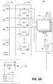
- FIG. 1A is a functional block diagram of a system 100 for detecting droops in the supply voltages and appropriately adjusting the clock frequency in accordance with one embodiment of the present disclosure.
- the system 100 includes a power source 110, a central processing unit (CPU) 120, a droop detector 130, and a clock generator 150 in accordance with one embodiment of the present disclosure.
- the power source 110 includes a plurality of power supplies 112, 114, 116, 118 supplying voltages Vdd 0 , Vdd 1 , Vdd 2 , Vdd n , respectively.
- the CPU 120 includes a plurality of cores 122, 124, 126, 128 receiving voltages Vdd 0 , Vdd 1 , Vdd 2 , Vdd n , respectively.
- the droop detector 130 includes a plurality of detector modules 132, 134, 136, 138 also receiving Vdd 0 , Vdd 1 , Vdd 2 , Vdd n , respectively, and a comparator 140. That is, module 132 receives Vdd 0 , module 134 receives Vdd 1 , module 136 receives Vdd 2 , and module 138 receives Vdd n . Outputs of the detector modules 132, 134, 136, 138 are tied together to form a single output (V out ) for the droop detector 130.
- the output of the detector modules 132, 134, 136, 138 (V out ) is coupled to one of the inputs of the comparator 140, which compares V out with a reference voltage (V ref ) and outputs a control signal (V control ) when V out falls below V ref .
- V ref a reference voltage
- V control a control signal
- the outputs of the detector modules 132, 134, 136, 138 (V out ) are coupled to the comparator 140 through a bandpass filter 142 to only pass frequencies of the output voltage within a predetermined range.
- the clock generator 150 includes a phase-locked loop (PLL) 152, a frequency divider unit 154, and a diplexer 156, which receives two inputs: (1) a direct output of the PLL; and (2) a divide-by-N output of the PLL.
- the divide-by-N output of the PLL has N-times the duration of the direct output of the PLL and its phase may be coherent with the phase of the direct output of the PLL.
- the output of the comparator 140 controls the diplexer 156 to select one of the two clock signals.
- the output signal of the comparator 140 selects the divide-by-N output of the PLL at the diplexer 156 (selects "1" input). Otherwise, the output signal of the comparator 140 selects the direct output of the PLL at the diplexer 156 (selects "0" input).
- the output of the clock generator 150 is tied to the clock inputs of the plurality of cores 122, 124, 126, 128.
- FIG. 1B is a functional block diagram of a system 160 for detecting droops in the supply voltages and appropriately adjusting the clock frequency in accordance with another embodiment of the present disclosure.
- the system 160 includes all of the modules that were included in the system 100 shown in FIG. 1A , but the system 160 further includes a dedicated frequency divider 170, 172, 174, or 176 for each core at its clock input.
- the operational frequency of each core can be configured to be a fraction of the global clock frequency.
- a divider ratio i.e., N 0 , N 1 , N 2 , ... N n
- the dedicated frequency divider 170, 172, 174, or 176 for each core can be same or different depending on the desired interface among cores.
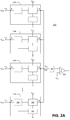
- FIG. 2A is a functional block diagram of the droop detector 130 including detector modules 132, 134, 136, 138 in accordance with one embodiment of the present disclosure.
- the droop detector 130 includes a plurality of input nodes (in 0 , in 1 , in 2 , ..., in n ), an output node (out), and a plurality of detector modules 132, 134, 136, 138.
- Each input node is configured to receive a supply voltage (V dd0 , V dd1 , V dd2 , ..., or V ddn ).
- the output node (out) is configured to output an output voltage (V out ).
- Each detector module 132, 134, 136, or 138 includes an input terminal (A) coupled to each input node (in 0 , in 1 , in 2 , ..., or in n ), an output terminal (B) coupled to the output node (out), and an input tracking unit 220 coupled to the input terminal (A) and the output terminal (B).
- the input tracking unit 220 is configured to: (a) follow variations of the supply voltage at the input node onto the output terminal (a voltage follower) when droop is detected on the supply voltage; or (b) temporarily disconnect the output terminal from the output node when no droop is detected on the supply voltage.
- each detector module 132, 134, 136, or 138 further includes an alternating current coupling module 210 disposed between the input terminal (A) and the input tracking unit 220, and is configured to form a high pass filter including a capacitor and a resistor.
- Each detector module 132, 134, 136, or 138 further includes an offset cancelling module 230 configured to substantially reduce mismatch-induced droop-detection range differences among the plurality of detector modules when the output terminals are coupled together at the output node.
- the offset cancelling module 230 is coupled to the input tracking unit 220 and the alternating current (AC) coupling module 210.
- the droop detector 130 further includes a comparator 140 configured to receive and compare the output voltage (V out ) to a reference voltage (V ref ).
- V ref a reference voltage
- the outputs of the detector modules 132, 134, 136, 138 (V out ) can be coupled to the comparator 140 through a bandpass filter 142 to only pass frequencies of the output voltage within a predetermined range.
- FIG. 2B is a schematic diagram of the detector modules 132, 134, 136, 138 of the droop detector 130 in accordance with one embodiment of the present disclosure.
- the illustrated embodiment of FIG. 2B shows only the schematic diagram of the detector module 138 receiving supply voltage Vdd n because it is at the top of the cascade of detector modules.
- each of the other detector modules 132, 134, 136 includes same elements with a same schematic diagram as that of the detector module 138. The only difference is the input supply voltage.
- Detector module 132 receives supply voltage Vdd 0
- detector module 134 receives supply voltage Vdd 1
- detector module 136 receives supply voltage Vdd 2 .
- outputs of the detector modules 132, 134, 136, 138 are tied together to form a single output (V out ).
- FIG. 2B shows the detector module 138 including an AC coupling module 210, an input tracking unit 220, and an offset cancelling module 230.
- the AC coupling module 210 includes a capacitor 212 and a resistor 214 forming a high pass filter to track only input variations above a desired frequency, which can be adjusted by varying the values of the capacitor 212 and the resistor 214.
- the AC coupling module 210 also avoids providing a DC load to the power source driving the droop detector 130.
- the input tracking unit 220 includes an operational amplifier (op amp) 222 and a p-type metal-oxide semiconductor field-effect transistor (p-MOSFET or PMOS transistor) 224 forming a voltage follower.
- the PMOS transistor 224 includes a gate terminal, a source terminal, and a drain terminal.
- the op amp 222 includes an output pin coupled to the gate terminal of the PMOS transistor, a negative input pin coupled to the source terminal, and a positive input pin coupled to the input terminal of each detector module through a capacitor of the AC coupling module.
- the negative input terminal (in n ) of the op amp 222 follows the positive input terminal (in p ) of the op amp 222.
- the use of the PMOS transistor 224 enables the input tracking unit 220 to track and detect negative-going voltages at in p .
- an n-type metal-oxide semiconductor field-effect transistor can be used to enable the input tracking unit 220 to track and detect positive-going voltages at in p .
- the offset cancelling module 230 includes PMOS transistor 232, a resistor 234, a capacitor 236, a current source 238, and an NMOS transistor 240 referred to as a voltage clamp.
- the offset cancelling module 230 is configured to substantially reduce mismatch-induced droop-detection range differences among the detector modules 132, 134, 136, 138 when the outputs of those units are tied together.
- Current sources 250, 252 provide an appropriate amount of current for proper operation of the detector module 130.
- the current source 252 is coupled to a voltage source (V DD ) and the source terminal of the PMOS transistor 224.
- the current source 250 is coupled to the voltage source and the PMOS transistor 232.
- FIG. 3A shows a connection of the outputs of the two detector modules 132, 134 in the droop detector 130 in accordance with one embodiment of the present disclosure.
- the detector module 132 receives supply voltage Vdd 0
- the detector module 134 receives supply voltage Vddi.
- the output terminal 312 of the detector module 132 is connected to the output terminal 314 of the detector module 134.
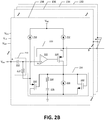
- FIG. 3B shows the operation of the two detector modules 132, 134 connected together at an output node 310 in accordance with one example embodiment of the present disclosure.
- the detector module 132 receives supply voltage Vdd 0 , which includes droop 350 from a nominal voltage, while the detector module 134 receives supply voltage Vdd 1 , with no droop 354 in the voltage.
- the positive input terminal (in p ) of the op amp 222 0 in the detector module 132 tracks the droop 350, which is reflected at the output of op amp 222 0 as a negative spike 351, and at the negative input terminal (in n ) of the op amp 222 0 and the output terminal 312 of the detector module 132 as a negative voltage spike 352.
- the negative voltage spike 351 causes the PMOS transistor 224 0 to conduct so that the output terminal 312 of the detector module 132 indicates that there is droop in the supply voltage Vdd 0 . This process is included in an input tracking loop 320.
- the positive input terminal (in p ) of the op amp 222 1 in the detector module 134 retains its biasing voltage as there is no droop (e.g., input 354) in the supply voltage Vddi.
- the negative input terminal (in n ) of the detector module 134 should follow the positive input terminal (in p ), the result is different.
- the negative input terminal (in n ) of the op amp 222 1 in the detector module 134 is connected to the negative input terminal (in n ) of the op amp 222 0 in the detector module 132 (because the output terminal 312 is connected to the output terminal 314 through the output node 310), the negative spike 352 at the negative input terminal (in n ) of the op amp 222 0 in the detector module 132 causes op amp 222 1 in the detector module 134 to output a positive-going pulse 360, which turns the PMOS transistor 224 1 off. This process is included in a non-linear feedback loop 370.
- the non-linear feedback loop 370 of each detector module is configured to temporarily disable detector modules that are detecting no droop (e.g., input 354) at their respective inputs while other detector modules are detecting a droop at their respective inputs (e.g., input 350).
- the droop detector 130 prevents the detector modules with no droop detection from degrading the gain of the output (V out ).
- the configuration of the droop detector 130 also includes an offset cancelling loop 330 which operates to substantially reduce mismatch-induced droop-detection range differences among detector modules 132, 134, 136, 138 when their outputs are tied together.
- FIG. 4 is a functional block diagram of an apparatus 400 configured to detect droops using a multi-input, multi-stage scalable detector with a non-linear feedback to disable stages with no droop transitions to avoid gain degradation in accordance with one embodiment of the present disclosure.
- the apparatus 400 includes multiple supply voltage receiving units 410, an output coupling unit 420, and multiple detector modules 430.
- Each supply voltage receiving unit 410 is configured to receive a supply voltage (V dd0 , V dd1 , V dd2 , ..., or V ddn ).
- the output coupling unit 420 is configured to couple the outputs of the multiple detector modules 430 and output an output voltage (V out ) at an output terminal.
- Each detector module 430 is coupled to each supply voltage receiving unit 410.
- Each detector module 430 also includes an input tracking unit configured to: (a) follow variations of the supply voltage at each supply voltage receiving unit 410 onto the output terminal when droop is detected on the supply voltage; or (b) temporarily disconnect the output terminal when no droop is detected on the supply voltage.
- Each detector module 430 further includes an alternating current (AC) coupling unit to form a high pass filter and an offset cancelling unit configured to substantially reduce mismatch-induced droop-detection range differences among the multiple detector modules 430 when the output terminals are coupled together.
- the apparatus 400 further includes a comparator unit 440 configured to receive and compare the output voltage (V out ) to a reference voltage (V ref ).
- processors such as a general purpose processor, a digital signal processor (DSP), an application specific integrated circuit (ASIC), a field programmable gate array (FPGA) or other programmable logic device, discrete gate or transistor logic, discrete hardware components, or any combination thereof designed to perform the functions described herein.
- DSP digital signal processor
- ASIC application specific integrated circuit
- FPGA field programmable gate array
- a general-purpose processor can be a microprocessor, but in the alternative, the processor can be any processor, controller, microcontroller, or state machine.
- a processor can also be implemented as a combination of computing devices, for example, a combination of a DSP and a microprocessor, a plurality of microprocessors, one or more microprocessors in conjunction with a DSP core, or any other such configuration. Further, circuits implementing the embodiments and functional blocks and modules described herein can be realized using various transistor types, logic families, and design methodologies.
Landscapes
- Engineering & Computer Science (AREA)
- Physics & Mathematics (AREA)
- General Physics & Mathematics (AREA)
- Theoretical Computer Science (AREA)
- General Engineering & Computer Science (AREA)
- Power Engineering (AREA)
- Computer Hardware Design (AREA)
- Computing Systems (AREA)
- Mathematical Physics (AREA)
- Measurement Of Current Or Voltage (AREA)
Applications Claiming Priority (2)
| Application Number | Priority Date | Filing Date | Title |
|---|---|---|---|
| US14/670,996 US9680391B2 (en) | 2015-03-27 | 2015-03-27 | Multi-input scalable rectifier droop detector |
| PCT/US2016/024189 WO2016160559A1 (en) | 2015-03-27 | 2016-03-25 | Multi-input scalable rectifier droop detector |
Publications (2)
| Publication Number | Publication Date |
|---|---|
| EP3274728A1 EP3274728A1 (en) | 2018-01-31 |
| EP3274728B1 true EP3274728B1 (en) | 2019-10-23 |
Family
ID=55745819
Family Applications (1)
| Application Number | Title | Priority Date | Filing Date |
|---|---|---|---|
| EP16715947.4A Active EP3274728B1 (en) | 2015-03-27 | 2016-03-25 | Multi-input scalable rectifier droop detector |
Country Status (6)
| Country | Link |
|---|---|
| US (1) | US9680391B2 (enExample) |
| EP (1) | EP3274728B1 (enExample) |
| JP (1) | JP6732786B2 (enExample) |
| KR (1) | KR102479541B1 (enExample) |
| CN (1) | CN107407700B (enExample) |
| WO (1) | WO2016160559A1 (enExample) |
Families Citing this family (6)
| Publication number | Priority date | Publication date | Assignee | Title |
|---|---|---|---|---|
| US10345883B2 (en) | 2016-05-31 | 2019-07-09 | Taiwan Semiconductor Manufacturing Co., Ltd. | Power estimation |
| US10552250B2 (en) | 2017-10-10 | 2020-02-04 | International Business Machines Corporation | Proactive voltage droop reduction and/or mitigation in a processor core |
| US11119126B2 (en) | 2019-07-23 | 2021-09-14 | International Business Machines Corporation | Slope detector for voltage droop monitoring |
| US10742202B1 (en) | 2019-07-23 | 2020-08-11 | International Business Machines Corporation | Autozero to an offset value for a slope detector for voltage droop monitoring |
| US11281248B2 (en) * | 2020-02-12 | 2022-03-22 | Nuvoton Technology Corporation | Audio microphone detection using auto-tracking current comparator |
| US11640193B2 (en) * | 2021-09-24 | 2023-05-02 | Qualcomm Incorporated | Detecting power delivery network marginality in a computing device |
Family Cites Families (17)
| Publication number | Priority date | Publication date | Assignee | Title |
|---|---|---|---|---|
| JPS62135532U (enExample) * | 1986-02-18 | 1987-08-26 | ||
| JP2730348B2 (ja) * | 1991-10-11 | 1998-03-25 | ヤマハ株式会社 | 電池式電子機器 |
| JP3295833B2 (ja) * | 1995-12-22 | 2002-06-24 | 日本電気エンジニアリング株式会社 | 電源冗長システム |
| JP2003241859A (ja) * | 2002-02-07 | 2003-08-29 | Internatl Business Mach Corp <Ibm> | 給電システムおよび該給電システムを含むラックマウント式コンピュータ・システム |
| US6670794B1 (en) | 2002-07-12 | 2003-12-30 | Richtek Technology Corp. | Multi-phase DC-to-DC buck converter with multi-phase current balance and adjustable load regulation |
| US7528619B2 (en) * | 2005-06-30 | 2009-05-05 | Intel Corporation | 0th droop detector architecture and implementation |
| US7480810B2 (en) | 2006-02-14 | 2009-01-20 | International Business Machines Corporation | Voltage droop dynamic recovery |
| US7902805B2 (en) * | 2006-04-03 | 2011-03-08 | Texas Instruments Deutschland Gmbh | Self-oscillating DC-DC buck converter with zero hysteresis |
| JP2010054217A (ja) * | 2008-08-26 | 2010-03-11 | Denso Corp | 電圧低下検出回路 |
| US8648645B2 (en) * | 2010-05-25 | 2014-02-11 | Oracle International Corporation | Microprocessor performance and power optimization through self calibrated inductive voltage droop monitoring and correction |
| TWM443878U (en) | 2012-07-23 | 2012-12-21 | Richtek Technology Corp | Multi-phase switching regulator and droop circuit therefor |
| TWI479768B (zh) | 2012-08-14 | 2015-04-01 | 台達電子工業股份有限公司 | 主動均流及降壓均流合併應用之電源系統及電源系統組合 |
| AU2013323342B2 (en) | 2012-09-28 | 2017-09-07 | Fluidic, Inc. | Droop compensation using current feedback |
| US9484860B2 (en) | 2013-03-12 | 2016-11-01 | Thx Ltd. | Tracking power supply with increased boost capability |
| US9696350B2 (en) | 2013-03-15 | 2017-07-04 | Intel Corporation | Non-linear control for voltage regulator |
| US8933737B1 (en) | 2013-06-28 | 2015-01-13 | Stmicroelectronics International N.V. | System and method for variable frequency clock generation |
| JP2015055598A (ja) * | 2013-09-13 | 2015-03-23 | アルプス電気株式会社 | 電圧検出装置 |
-
2015
- 2015-03-27 US US14/670,996 patent/US9680391B2/en active Active
-
2016
- 2016-03-25 CN CN201680017013.7A patent/CN107407700B/zh active Active
- 2016-03-25 WO PCT/US2016/024189 patent/WO2016160559A1/en not_active Ceased
- 2016-03-25 EP EP16715947.4A patent/EP3274728B1/en active Active
- 2016-03-25 JP JP2017550179A patent/JP6732786B2/ja not_active Expired - Fee Related
- 2016-03-25 KR KR1020177027097A patent/KR102479541B1/ko active Active
Non-Patent Citations (1)
| Title |
|---|
| None * |
Also Published As
| Publication number | Publication date |
|---|---|
| WO2016160559A1 (en) | 2016-10-06 |
| US20160285385A1 (en) | 2016-09-29 |
| KR20170131456A (ko) | 2017-11-29 |
| JP2018512589A (ja) | 2018-05-17 |
| JP6732786B2 (ja) | 2020-07-29 |
| CN107407700A (zh) | 2017-11-28 |
| KR102479541B1 (ko) | 2022-12-19 |
| US9680391B2 (en) | 2017-06-13 |
| CN107407700B (zh) | 2019-12-27 |
| EP3274728A1 (en) | 2018-01-31 |
Similar Documents
| Publication | Publication Date | Title |
|---|---|---|
| EP3274728B1 (en) | Multi-input scalable rectifier droop detector | |
| US9525407B2 (en) | Power monitoring circuit, and a power up reset generator | |
| US9647469B2 (en) | Charge and discharge control circuit, charge and discharge control unit, and battery device | |
| US20170077933A1 (en) | Phase-Locked Loop Circuit, Data Recovery Circuit, and Control Method for Phase-Locked Loop Circuit | |
| US7859421B2 (en) | Circuit and method for detecting a voltage change | |
| US20150372601A1 (en) | Power supply system and short circuit and/or bad connection detection method thereof, and power converter thereof | |
| US8843093B2 (en) | Low power squelch detector circuit | |
| US10263440B2 (en) | Short-circuit determination method and electronic device | |
| US9843256B2 (en) | Internal voltage generation circuit | |
| US9274148B2 (en) | Voltage detection circuit | |
| JP2018512589A5 (enExample) | ||
| US20180138691A1 (en) | Integrated circuit with reverse current protection and power source disconnection detection | |
| US9343977B2 (en) | Power conversion apparatus and over power protection method thereof | |
| US9166468B2 (en) | Voltage regulator circuit with soft-start function | |
| EP3018828B1 (en) | Phase detector | |
| US20190393868A1 (en) | External and dual ramp clock synchronization | |
| EP3239800B1 (en) | Electronic device | |
| EP1679575A2 (en) | Signal detection method, frequency detection method, power consumption control method, signal detecting device, frequency detecting device, power consumption control device and electronic apparatus | |
| US9341661B2 (en) | Tone detector | |
| US10715114B1 (en) | Filter and operating method thereof | |
| US10333529B1 (en) | Method of forming a conversion circuit and structure therefor | |
| CN105099448B (zh) | 可调式振荡装置 | |
| US20220416796A1 (en) | Initialization circuit of delay locked loop | |
| US20200292614A1 (en) | Semiconductor integrated circuit | |
| TWI448872B (zh) | 電流供應系統、使用此電流供應系統的類比數位轉換器以及電流供應方法 |
Legal Events
| Date | Code | Title | Description |
|---|---|---|---|
| STAA | Information on the status of an ep patent application or granted ep patent |
Free format text: STATUS: THE INTERNATIONAL PUBLICATION HAS BEEN MADE |
|
| PUAI | Public reference made under article 153(3) epc to a published international application that has entered the european phase |
Free format text: ORIGINAL CODE: 0009012 |
|
| STAA | Information on the status of an ep patent application or granted ep patent |
Free format text: STATUS: REQUEST FOR EXAMINATION WAS MADE |
|
| 17P | Request for examination filed |
Effective date: 20170816 |
|
| AK | Designated contracting states |
Kind code of ref document: A1 Designated state(s): AL AT BE BG CH CY CZ DE DK EE ES FI FR GB GR HR HU IE IS IT LI LT LU LV MC MK MT NL NO PL PT RO RS SE SI SK SM TR |
|
| AX | Request for extension of the european patent |
Extension state: BA ME |
|
| DAV | Request for validation of the european patent (deleted) | ||
| DAX | Request for extension of the european patent (deleted) | ||
| GRAP | Despatch of communication of intention to grant a patent |
Free format text: ORIGINAL CODE: EPIDOSNIGR1 |
|
| STAA | Information on the status of an ep patent application or granted ep patent |
Free format text: STATUS: GRANT OF PATENT IS INTENDED |
|
| INTG | Intention to grant announced |
Effective date: 20190509 |
|
| GRAS | Grant fee paid |
Free format text: ORIGINAL CODE: EPIDOSNIGR3 |
|
| GRAA | (expected) grant |
Free format text: ORIGINAL CODE: 0009210 |
|
| STAA | Information on the status of an ep patent application or granted ep patent |
Free format text: STATUS: THE PATENT HAS BEEN GRANTED |
|
| AK | Designated contracting states |
Kind code of ref document: B1 Designated state(s): AL AT BE BG CH CY CZ DE DK EE ES FI FR GB GR HR HU IE IS IT LI LT LU LV MC MK MT NL NO PL PT RO RS SE SI SK SM TR |
|
| REG | Reference to a national code |
Ref country code: GB Ref legal event code: FG4D |
|
| REG | Reference to a national code |
Ref country code: CH Ref legal event code: EP |
|
| REG | Reference to a national code |
Ref country code: IE Ref legal event code: FG4D |
|
| REG | Reference to a national code |
Ref country code: DE Ref legal event code: R096 Ref document number: 602016022896 Country of ref document: DE |
|
| REG | Reference to a national code |
Ref country code: AT Ref legal event code: REF Ref document number: 1194254 Country of ref document: AT Kind code of ref document: T Effective date: 20191115 |
|
| REG | Reference to a national code |
Ref country code: NL Ref legal event code: MP Effective date: 20191023 |
|
| PGFP | Annual fee paid to national office [announced via postgrant information from national office to epo] |
Ref country code: FR Payment date: 20191023 Year of fee payment: 5 |
|
| REG | Reference to a national code |
Ref country code: LT Ref legal event code: MG4D |
|
| PG25 | Lapsed in a contracting state [announced via postgrant information from national office to epo] |
Ref country code: SE Free format text: LAPSE BECAUSE OF FAILURE TO SUBMIT A TRANSLATION OF THE DESCRIPTION OR TO PAY THE FEE WITHIN THE PRESCRIBED TIME-LIMIT Effective date: 20191023 Ref country code: LV Free format text: LAPSE BECAUSE OF FAILURE TO SUBMIT A TRANSLATION OF THE DESCRIPTION OR TO PAY THE FEE WITHIN THE PRESCRIBED TIME-LIMIT Effective date: 20191023 Ref country code: BG Free format text: LAPSE BECAUSE OF FAILURE TO SUBMIT A TRANSLATION OF THE DESCRIPTION OR TO PAY THE FEE WITHIN THE PRESCRIBED TIME-LIMIT Effective date: 20200123 Ref country code: PT Free format text: LAPSE BECAUSE OF FAILURE TO SUBMIT A TRANSLATION OF THE DESCRIPTION OR TO PAY THE FEE WITHIN THE PRESCRIBED TIME-LIMIT Effective date: 20200224 Ref country code: FI Free format text: LAPSE BECAUSE OF FAILURE TO SUBMIT A TRANSLATION OF THE DESCRIPTION OR TO PAY THE FEE WITHIN THE PRESCRIBED TIME-LIMIT Effective date: 20191023 Ref country code: GR Free format text: LAPSE BECAUSE OF FAILURE TO SUBMIT A TRANSLATION OF THE DESCRIPTION OR TO PAY THE FEE WITHIN THE PRESCRIBED TIME-LIMIT Effective date: 20200124 Ref country code: NO Free format text: LAPSE BECAUSE OF FAILURE TO SUBMIT A TRANSLATION OF THE DESCRIPTION OR TO PAY THE FEE WITHIN THE PRESCRIBED TIME-LIMIT Effective date: 20200123 Ref country code: PL Free format text: LAPSE BECAUSE OF FAILURE TO SUBMIT A TRANSLATION OF THE DESCRIPTION OR TO PAY THE FEE WITHIN THE PRESCRIBED TIME-LIMIT Effective date: 20191023 Ref country code: NL Free format text: LAPSE BECAUSE OF FAILURE TO SUBMIT A TRANSLATION OF THE DESCRIPTION OR TO PAY THE FEE WITHIN THE PRESCRIBED TIME-LIMIT Effective date: 20191023 Ref country code: LT Free format text: LAPSE BECAUSE OF FAILURE TO SUBMIT A TRANSLATION OF THE DESCRIPTION OR TO PAY THE FEE WITHIN THE PRESCRIBED TIME-LIMIT Effective date: 20191023 |
|
| PG25 | Lapsed in a contracting state [announced via postgrant information from national office to epo] |
Ref country code: HR Free format text: LAPSE BECAUSE OF FAILURE TO SUBMIT A TRANSLATION OF THE DESCRIPTION OR TO PAY THE FEE WITHIN THE PRESCRIBED TIME-LIMIT Effective date: 20191023 Ref country code: RS Free format text: LAPSE BECAUSE OF FAILURE TO SUBMIT A TRANSLATION OF THE DESCRIPTION OR TO PAY THE FEE WITHIN THE PRESCRIBED TIME-LIMIT Effective date: 20191023 Ref country code: IS Free format text: LAPSE BECAUSE OF FAILURE TO SUBMIT A TRANSLATION OF THE DESCRIPTION OR TO PAY THE FEE WITHIN THE PRESCRIBED TIME-LIMIT Effective date: 20200224 |
|
| PG25 | Lapsed in a contracting state [announced via postgrant information from national office to epo] |
Ref country code: AL Free format text: LAPSE BECAUSE OF FAILURE TO SUBMIT A TRANSLATION OF THE DESCRIPTION OR TO PAY THE FEE WITHIN THE PRESCRIBED TIME-LIMIT Effective date: 20191023 |
|
| REG | Reference to a national code |
Ref country code: DE Ref legal event code: R097 Ref document number: 602016022896 Country of ref document: DE |
|
| PG2D | Information on lapse in contracting state deleted |
Ref country code: IS |
|
| PG25 | Lapsed in a contracting state [announced via postgrant information from national office to epo] |
Ref country code: EE Free format text: LAPSE BECAUSE OF FAILURE TO SUBMIT A TRANSLATION OF THE DESCRIPTION OR TO PAY THE FEE WITHIN THE PRESCRIBED TIME-LIMIT Effective date: 20191023 Ref country code: CZ Free format text: LAPSE BECAUSE OF FAILURE TO SUBMIT A TRANSLATION OF THE DESCRIPTION OR TO PAY THE FEE WITHIN THE PRESCRIBED TIME-LIMIT Effective date: 20191023 Ref country code: RO Free format text: LAPSE BECAUSE OF FAILURE TO SUBMIT A TRANSLATION OF THE DESCRIPTION OR TO PAY THE FEE WITHIN THE PRESCRIBED TIME-LIMIT Effective date: 20191023 Ref country code: ES Free format text: LAPSE BECAUSE OF FAILURE TO SUBMIT A TRANSLATION OF THE DESCRIPTION OR TO PAY THE FEE WITHIN THE PRESCRIBED TIME-LIMIT Effective date: 20191023 Ref country code: DK Free format text: LAPSE BECAUSE OF FAILURE TO SUBMIT A TRANSLATION OF THE DESCRIPTION OR TO PAY THE FEE WITHIN THE PRESCRIBED TIME-LIMIT Effective date: 20191023 Ref country code: IS Free format text: LAPSE BECAUSE OF FAILURE TO SUBMIT A TRANSLATION OF THE DESCRIPTION OR TO PAY THE FEE WITHIN THE PRESCRIBED TIME-LIMIT Effective date: 20200223 |
|
| REG | Reference to a national code |
Ref country code: AT Ref legal event code: MK05 Ref document number: 1194254 Country of ref document: AT Kind code of ref document: T Effective date: 20191023 |
|
| PLBE | No opposition filed within time limit |
Free format text: ORIGINAL CODE: 0009261 |
|
| STAA | Information on the status of an ep patent application or granted ep patent |
Free format text: STATUS: NO OPPOSITION FILED WITHIN TIME LIMIT |
|
| PG25 | Lapsed in a contracting state [announced via postgrant information from national office to epo] |
Ref country code: SM Free format text: LAPSE BECAUSE OF FAILURE TO SUBMIT A TRANSLATION OF THE DESCRIPTION OR TO PAY THE FEE WITHIN THE PRESCRIBED TIME-LIMIT Effective date: 20191023 Ref country code: IT Free format text: LAPSE BECAUSE OF FAILURE TO SUBMIT A TRANSLATION OF THE DESCRIPTION OR TO PAY THE FEE WITHIN THE PRESCRIBED TIME-LIMIT Effective date: 20191023 Ref country code: SK Free format text: LAPSE BECAUSE OF FAILURE TO SUBMIT A TRANSLATION OF THE DESCRIPTION OR TO PAY THE FEE WITHIN THE PRESCRIBED TIME-LIMIT Effective date: 20191023 |
|
| 26N | No opposition filed |
Effective date: 20200724 |
|
| PG25 | Lapsed in a contracting state [announced via postgrant information from national office to epo] |
Ref country code: MC Free format text: LAPSE BECAUSE OF FAILURE TO SUBMIT A TRANSLATION OF THE DESCRIPTION OR TO PAY THE FEE WITHIN THE PRESCRIBED TIME-LIMIT Effective date: 20191023 |
|
| REG | Reference to a national code |
Ref country code: CH Ref legal event code: PL |
|
| PG25 | Lapsed in a contracting state [announced via postgrant information from national office to epo] |
Ref country code: SI Free format text: LAPSE BECAUSE OF FAILURE TO SUBMIT A TRANSLATION OF THE DESCRIPTION OR TO PAY THE FEE WITHIN THE PRESCRIBED TIME-LIMIT Effective date: 20191023 Ref country code: AT Free format text: LAPSE BECAUSE OF FAILURE TO SUBMIT A TRANSLATION OF THE DESCRIPTION OR TO PAY THE FEE WITHIN THE PRESCRIBED TIME-LIMIT Effective date: 20191023 |
|
| REG | Reference to a national code |
Ref country code: BE Ref legal event code: MM Effective date: 20200331 |
|
| PG25 | Lapsed in a contracting state [announced via postgrant information from national office to epo] |
Ref country code: LU Free format text: LAPSE BECAUSE OF NON-PAYMENT OF DUE FEES Effective date: 20200325 |
|
| PG25 | Lapsed in a contracting state [announced via postgrant information from national office to epo] |
Ref country code: LI Free format text: LAPSE BECAUSE OF NON-PAYMENT OF DUE FEES Effective date: 20200331 Ref country code: IE Free format text: LAPSE BECAUSE OF NON-PAYMENT OF DUE FEES Effective date: 20200325 Ref country code: CH Free format text: LAPSE BECAUSE OF NON-PAYMENT OF DUE FEES Effective date: 20200331 |
|
| PG25 | Lapsed in a contracting state [announced via postgrant information from national office to epo] |
Ref country code: BE Free format text: LAPSE BECAUSE OF NON-PAYMENT OF DUE FEES Effective date: 20200331 |
|
| PG25 | Lapsed in a contracting state [announced via postgrant information from national office to epo] |
Ref country code: FR Free format text: LAPSE BECAUSE OF NON-PAYMENT OF DUE FEES Effective date: 20210331 |
|
| PG25 | Lapsed in a contracting state [announced via postgrant information from national office to epo] |
Ref country code: TR Free format text: LAPSE BECAUSE OF FAILURE TO SUBMIT A TRANSLATION OF THE DESCRIPTION OR TO PAY THE FEE WITHIN THE PRESCRIBED TIME-LIMIT Effective date: 20191023 Ref country code: MT Free format text: LAPSE BECAUSE OF FAILURE TO SUBMIT A TRANSLATION OF THE DESCRIPTION OR TO PAY THE FEE WITHIN THE PRESCRIBED TIME-LIMIT Effective date: 20191023 Ref country code: CY Free format text: LAPSE BECAUSE OF FAILURE TO SUBMIT A TRANSLATION OF THE DESCRIPTION OR TO PAY THE FEE WITHIN THE PRESCRIBED TIME-LIMIT Effective date: 20191023 |
|
| PG25 | Lapsed in a contracting state [announced via postgrant information from national office to epo] |
Ref country code: MK Free format text: LAPSE BECAUSE OF FAILURE TO SUBMIT A TRANSLATION OF THE DESCRIPTION OR TO PAY THE FEE WITHIN THE PRESCRIBED TIME-LIMIT Effective date: 20191023 |
|
| PGFP | Annual fee paid to national office [announced via postgrant information from national office to epo] |
Ref country code: DE Payment date: 20250210 Year of fee payment: 10 |
|
| PGFP | Annual fee paid to national office [announced via postgrant information from national office to epo] |
Ref country code: GB Payment date: 20250213 Year of fee payment: 10 |