EP3273754A1 - Stretchable cable and stretchable circuit board - Google Patents
Stretchable cable and stretchable circuit board Download PDFInfo
- Publication number
- EP3273754A1 EP3273754A1 EP16764943.3A EP16764943A EP3273754A1 EP 3273754 A1 EP3273754 A1 EP 3273754A1 EP 16764943 A EP16764943 A EP 16764943A EP 3273754 A1 EP3273754 A1 EP 3273754A1
- Authority
- EP
- European Patent Office
- Prior art keywords
- stretchable
- substrate
- stretchable substrate
- wiring
- conductive filler
- Prior art date
- Legal status (The legal status is an assumption and is not a legal conclusion. Google has not performed a legal analysis and makes no representation as to the accuracy of the status listed.)
- Granted
Links
Images



Classifications
-
- H—ELECTRICITY
- H05—ELECTRIC TECHNIQUES NOT OTHERWISE PROVIDED FOR
- H05K—PRINTED CIRCUITS; CASINGS OR CONSTRUCTIONAL DETAILS OF ELECTRIC APPARATUS; MANUFACTURE OF ASSEMBLAGES OF ELECTRICAL COMPONENTS
- H05K1/00—Printed circuits
- H05K1/02—Details
- H05K1/0277—Bendability or stretchability details
- H05K1/0283—Stretchable printed circuits
-
- B—PERFORMING OPERATIONS; TRANSPORTING
- B32—LAYERED PRODUCTS
- B32B—LAYERED PRODUCTS, i.e. PRODUCTS BUILT-UP OF STRATA OF FLAT OR NON-FLAT, e.g. CELLULAR OR HONEYCOMB, FORM
- B32B27/00—Layered products comprising a layer of synthetic resin
- B32B27/18—Layered products comprising a layer of synthetic resin characterised by the use of special additives
-
- H—ELECTRICITY
- H01—ELECTRIC ELEMENTS
- H01B—CABLES; CONDUCTORS; INSULATORS; SELECTION OF MATERIALS FOR THEIR CONDUCTIVE, INSULATING OR DIELECTRIC PROPERTIES
- H01B1/00—Conductors or conductive bodies characterised by the conductive materials; Selection of materials as conductors
- H01B1/20—Conductive material dispersed in non-conductive organic material
- H01B1/22—Conductive material dispersed in non-conductive organic material the conductive material comprising metals or alloys
-
- H—ELECTRICITY
- H01—ELECTRIC ELEMENTS
- H01B—CABLES; CONDUCTORS; INSULATORS; SELECTION OF MATERIALS FOR THEIR CONDUCTIVE, INSULATING OR DIELECTRIC PROPERTIES
- H01B7/00—Insulated conductors or cables characterised by their form
- H01B7/0009—Details relating to the conductive cores
-
- H—ELECTRICITY
- H01—ELECTRIC ELEMENTS
- H01B—CABLES; CONDUCTORS; INSULATORS; SELECTION OF MATERIALS FOR THEIR CONDUCTIVE, INSULATING OR DIELECTRIC PROPERTIES
- H01B7/00—Insulated conductors or cables characterised by their form
- H01B7/04—Flexible cables, conductors, or cords, e.g. trailing cables
-
- H—ELECTRICITY
- H01—ELECTRIC ELEMENTS
- H01B—CABLES; CONDUCTORS; INSULATORS; SELECTION OF MATERIALS FOR THEIR CONDUCTIVE, INSULATING OR DIELECTRIC PROPERTIES
- H01B7/00—Insulated conductors or cables characterised by their form
- H01B7/06—Extensible conductors or cables, e.g. self-coiling cords
-
- H—ELECTRICITY
- H01—ELECTRIC ELEMENTS
- H01B—CABLES; CONDUCTORS; INSULATORS; SELECTION OF MATERIALS FOR THEIR CONDUCTIVE, INSULATING OR DIELECTRIC PROPERTIES
- H01B7/00—Insulated conductors or cables characterised by their form
- H01B7/08—Flat or ribbon cables
-
- H—ELECTRICITY
- H05—ELECTRIC TECHNIQUES NOT OTHERWISE PROVIDED FOR
- H05K—PRINTED CIRCUITS; CASINGS OR CONSTRUCTIONAL DETAILS OF ELECTRIC APPARATUS; MANUFACTURE OF ASSEMBLAGES OF ELECTRICAL COMPONENTS
- H05K1/00—Printed circuits
- H05K1/02—Details
- H05K1/09—Use of materials for the conductive, e.g. metallic pattern
-
- H—ELECTRICITY
- H05—ELECTRIC TECHNIQUES NOT OTHERWISE PROVIDED FOR
- H05K—PRINTED CIRCUITS; CASINGS OR CONSTRUCTIONAL DETAILS OF ELECTRIC APPARATUS; MANUFACTURE OF ASSEMBLAGES OF ELECTRICAL COMPONENTS
- H05K1/00—Printed circuits
- H05K1/02—Details
- H05K1/09—Use of materials for the conductive, e.g. metallic pattern
- H05K1/092—Dispersed materials, e.g. conductive pastes or inks
- H05K1/095—Dispersed materials, e.g. conductive pastes or inks for polymer thick films, i.e. having a permanent organic polymeric binder
-
- H—ELECTRICITY
- H05—ELECTRIC TECHNIQUES NOT OTHERWISE PROVIDED FOR
- H05K—PRINTED CIRCUITS; CASINGS OR CONSTRUCTIONAL DETAILS OF ELECTRIC APPARATUS; MANUFACTURE OF ASSEMBLAGES OF ELECTRICAL COMPONENTS
- H05K1/00—Printed circuits
- H05K1/02—Details
- H05K1/11—Printed elements for providing electric connections to or between printed circuits
- H05K1/115—Via connections; Lands around holes or via connections
-
- H—ELECTRICITY
- H05—ELECTRIC TECHNIQUES NOT OTHERWISE PROVIDED FOR
- H05K—PRINTED CIRCUITS; CASINGS OR CONSTRUCTIONAL DETAILS OF ELECTRIC APPARATUS; MANUFACTURE OF ASSEMBLAGES OF ELECTRICAL COMPONENTS
- H05K1/00—Printed circuits
- H05K1/18—Printed circuits structurally associated with non-printed electric components
- H05K1/181—Printed circuits structurally associated with non-printed electric components associated with surface mounted components
-
- H—ELECTRICITY
- H05—ELECTRIC TECHNIQUES NOT OTHERWISE PROVIDED FOR
- H05K—PRINTED CIRCUITS; CASINGS OR CONSTRUCTIONAL DETAILS OF ELECTRIC APPARATUS; MANUFACTURE OF ASSEMBLAGES OF ELECTRICAL COMPONENTS
- H05K3/00—Apparatus or processes for manufacturing printed circuits
- H05K3/10—Apparatus or processes for manufacturing printed circuits in which conductive material is applied to the insulating support in such a manner as to form the desired conductive pattern
- H05K3/12—Apparatus or processes for manufacturing printed circuits in which conductive material is applied to the insulating support in such a manner as to form the desired conductive pattern using thick film techniques, e.g. printing techniques to apply the conductive material or similar techniques for applying conductive paste or ink patterns
- H05K3/1283—After-treatment of the printed patterns, e.g. sintering or curing methods
-
- H—ELECTRICITY
- H05—ELECTRIC TECHNIQUES NOT OTHERWISE PROVIDED FOR
- H05K—PRINTED CIRCUITS; CASINGS OR CONSTRUCTIONAL DETAILS OF ELECTRIC APPARATUS; MANUFACTURE OF ASSEMBLAGES OF ELECTRICAL COMPONENTS
- H05K3/00—Apparatus or processes for manufacturing printed circuits
- H05K3/10—Apparatus or processes for manufacturing printed circuits in which conductive material is applied to the insulating support in such a manner as to form the desired conductive pattern
- H05K3/20—Apparatus or processes for manufacturing printed circuits in which conductive material is applied to the insulating support in such a manner as to form the desired conductive pattern by affixing prefabricated conductor pattern
- H05K3/207—Apparatus or processes for manufacturing printed circuits in which conductive material is applied to the insulating support in such a manner as to form the desired conductive pattern by affixing prefabricated conductor pattern using a prefabricated paste pattern, ink pattern or powder pattern
-
- H—ELECTRICITY
- H05—ELECTRIC TECHNIQUES NOT OTHERWISE PROVIDED FOR
- H05K—PRINTED CIRCUITS; CASINGS OR CONSTRUCTIONAL DETAILS OF ELECTRIC APPARATUS; MANUFACTURE OF ASSEMBLAGES OF ELECTRICAL COMPONENTS
- H05K3/00—Apparatus or processes for manufacturing printed circuits
- H05K3/30—Assembling printed circuits with electric components, e.g. with resistors
- H05K3/303—Assembling printed circuits with electric components, e.g. with resistors with surface mounted components
-
- H—ELECTRICITY
- H05—ELECTRIC TECHNIQUES NOT OTHERWISE PROVIDED FOR
- H05K—PRINTED CIRCUITS; CASINGS OR CONSTRUCTIONAL DETAILS OF ELECTRIC APPARATUS; MANUFACTURE OF ASSEMBLAGES OF ELECTRICAL COMPONENTS
- H05K3/00—Apparatus or processes for manufacturing printed circuits
- H05K3/40—Forming printed elements for providing electric connections to or between printed circuits
- H05K3/4038—Through-connections; Vertical interconnect access [VIA] connections
- H05K3/4053—Through-connections; Vertical interconnect access [VIA] connections by thick-film techniques
-
- H—ELECTRICITY
- H05—ELECTRIC TECHNIQUES NOT OTHERWISE PROVIDED FOR
- H05K—PRINTED CIRCUITS; CASINGS OR CONSTRUCTIONAL DETAILS OF ELECTRIC APPARATUS; MANUFACTURE OF ASSEMBLAGES OF ELECTRICAL COMPONENTS
- H05K3/00—Apparatus or processes for manufacturing printed circuits
- H05K3/46—Manufacturing multilayer circuits
-
- H—ELECTRICITY
- H05—ELECTRIC TECHNIQUES NOT OTHERWISE PROVIDED FOR
- H05K—PRINTED CIRCUITS; CASINGS OR CONSTRUCTIONAL DETAILS OF ELECTRIC APPARATUS; MANUFACTURE OF ASSEMBLAGES OF ELECTRICAL COMPONENTS
- H05K3/00—Apparatus or processes for manufacturing printed circuits
- H05K3/46—Manufacturing multilayer circuits
- H05K3/4644—Manufacturing multilayer circuits by building the multilayer layer by layer, i.e. build-up multilayer circuits
- H05K3/4664—Adding a circuit layer by thick film methods, e.g. printing techniques or by other techniques for making conductive patterns by using pastes, inks or powders
Definitions
- the present invention relates to a stretchable cable exhibiting elasticity and a stretchable circuit board exhibiting elasticity.
- a flexible printed circuit (FPC) board exhibits bendability, whereas does not exhibit elasticity.
- a circuit board has been known, which is configured such that a rigid substrate is stacked on a FPC etched in a wave shape (an accordion shape).
- the FPC can deform by twisting, but the FPC itself is not stretchable.
- Patent Literature 1 JP-T-2009-533839
- the present invention is intended to provide a stretchable cable exhibiting elasticity.
- the present invention is intended to provide a stretchable circuit board exhibiting elasticity.
- a stretchable cable according to the present invention includes a sheet-shaped base material exhibiting elasticity, and a wiring formed on one surface of the base material and exhibiting elasticity.
- the wiring is made of a conductive composition containing elastomer and a conductive filler filling the elastomer.
- the base material and the wiring exhibit elasticity.
- the stretchable cable exhibiting elasticity is obtained.
- the conductive filler includes a coil-shaped conductive filler.
- the coil-shaped conductive filler may be, for example, a small metal coil manufactured in such a manner that metal plating is applied to a natural helical structure.
- the coil-shaped conductive filler may be a small metal spring manufactured in such a manner that a metal wire is processed into a coil shape.
- the coil-shaped conductive filler may be a carbon nanocoil.
- the conductive filler includes the coil-shaped conductive filler.
- the conductive filler in the conductive composition stretches as in a pulled coil. Accordingly, even when the elastomer stretches, an increase in a resistance value of the wiring can be suppressed.
- the stretchable cable can be realized, which has the wiring exhibiting elasticity and configured so that an increase in the resistance value in stretching can be suppressed.
- the conductive filler includes a dendrite-shaped conductive filler.
- the dendrite shape indicates such a shape that a rod-shaped bifurcated branch extends from a rod-shaped main branch in a two-dimensional direction or a three-dimensional direction. Moreover, the dendrite shape also includes a shape in which the bifurcated branch bends in the middle, and a shape in which a rod-shaped bifurcated branch further extends from the middle of the bifurcated branch.
- the conductive filler includes the dendrite-shaped conductive filler. Even when the elastomer in the conductive composition is stretched, the probability of contacting the conductive fillers of the conductive composition each other can be improved. Thus, even in the case of stretching the elastomer, a conductive path can be satisfactorily formed in the elastomer. As a result, the stretchable cable can be realized, which has the wiring exhibiting elasticity and configured so that an increase in the resistance value in stretching can be suppressed.
- a first stretchable circuit board includes a stretchable substrate exhibiting elasticity, a non-stretchable substrate bonded to a partial region of one surface of the stretchable substrate and not exhibiting elasticity, and a stretchable wiring formed on the other surface of the stretchable substrate and exhibiting elasticity.
- the non-stretchable substrate not exhibiting elasticity is bonded to the partial region of one surface of the stretchable substrate exhibiting elasticity.
- An electronic component not exhibiting elasticity can be mounted on this non-stretchable substrate side.
- the stretchable wiring exhibiting elasticity is formed on the other surface of the stretchable substrate.
- the stretchable substrate and the stretchable wiring hold elasticity in a region to which the non-stretchable substrate is not bonded.
- the stretchable circuit board exhibiting elasticity is obtained.
- a conductor layer formed on the surface of the non-stretchable substrate opposite to the surface bonded to the stretchable substrate and a first via penetrating the stretchable substrate and the non-stretchable substrate and connecting the stretchable wiring and the conductor layer together are provided.
- the electronic component mounted on the non-stretchable substrate side can be connected to the stretchable wiring through the conductor layer and the first via.
- an insulating layer covering the conductor layer, an electronic component provided on a surface of the insulating layer, and a second via penetrating the insulating layer and electrically connecting the conductor layer and the electronic component together are provided.
- the electronic component can be connected to the stretchable wiring through the second via, the conductor layer, and the first via.
- a second stretchable circuit board includes a stretchable substrate exhibiting elasticity, a stretchable wiring formed on a portion of one surface of the stretchable substrate and exhibiting elasticity, and a non-stretchable substrate not exhibiting elasticity and bonded to a partial region of one surface of the stretchable substrate, the partial region including at least a portion of the stretchable wiring.
- the stretchable wiring exhibiting elasticity is formed in the partial region of one surface of the stretchable substrate exhibiting elasticity.
- the non-stretchable substrate not exhibiting elasticity is bonded to the partial region of one surface of the stretchable substrate, the partial region including at least a portion of the stretchable wiring.
- An electronic component not exhibiting elasticity can be mounted on this non-stretchable substrate side.
- the stretchable substrate and the stretchable wiring hold elasticity in a region to which the non-stretchable substrate is not bonded.
- the stretchable circuit board exhibiting elasticity is obtained.
- a conductor layer formed on the surface of the non-stretchable substrate opposite to the surface bonded to the stretchable substrate and a first via penetrating the non-stretchable substrate and connecting the stretchable wiring and the conductor layer together are further provided.
- the electronic component mounted on the non-stretchable substrate side can be connected to the stretchable wiring through the conductor layer and the first via.
- an insulating layer covering the conductor layer, an electronic component provided on a surface of the insulating layer, and a second via penetrating the insulating layer and electrically connecting the conductor layer and the electronic component together are further provided.
- the electronic component can be connected to the stretchable wiring through the second via, the conductor layer, and the first via.
- the non-stretchable substrate is a rigid substrate or a flexible substrate.
- Fig. 1 is a schematic cross-sectional view of a configuration of a stretchable cable of a first embodiment of the present invention.
- a stretchable cable 1 includes a sheet-shaped stretchable base material 2 exhibiting elasticity and elongated in one direction (a right-to-left direction in Fig. 1 ), and a stretchable wiring 3 formed on one surface of the stretchable base material 2 and exhibiting elasticity.
- the stretchable wiring 3 includes a plurality of stretchable wires 3a. The stretchable wires 3a extend in parallel to each other at intervals in a width direction of the stretchable base material 2.
- the stretchable base material 2 is made of a material exhibiting elasticity.
- elastomer e.g., polyurethane elastomer, styrene elastomer, olefin elastomer, polyamide elastomer, and silicone elastomer
- synthetic rubber e.g., ethylene-propylene rubber, nitrile-butadiene rubber, silicone rubber, acrylic rubber, fluorine rubber, and urethane rubber
- the stretchable wiring 3 is made of a conductive composition including elastomer and a conductive filler filling the elastomer.
- the shape of the conductive filler may be a coil shape, a dendrite shape, a block shape, a spherical shape, a flake shape, a needle shape, and a fiber shape.
- the conductive filler includes a conductive filler in the coil shape (hereinafter referred to as a "coil-shaped conductive filler").
- the coil shape includes a helical shape and a spiral shape.
- the conductive filler is in the coil shape.
- the stretchable cable 1 can be realized, which has the stretchable wiring 3 exhibiting elasticity and configured so that an increase in the resistance value in stretching can be suppressed.
- the elastomer is resin having elastic force, such as styrene elastomer, olefin elastomer, polyester elastomer, polyurethane elastomer, polyamide elastomer, and silicone elastomer.
- the polyurethane elastomer includes a hard segment and a soft segment.
- the soft segment includes, for example, carbonate, ester, and ether.
- NE-8880, MAU-9022, NE-310, NE-302HV, and CU-8448 etc. manufactured by Dainichiseika Color and Chemicals Mfg. Co., Ltd. can be used.
- the elastomer may be made of a single type of resin or multiple types of resin.
- the elastomer may contain an additive such as a plasticizing agent, a processing aid, a cross-linking agent, a vulcanization accelerator, a vulcanization aid, an anti-aging agent, a softening agent, and a coloring agent.
- an additive such as a plasticizing agent, a processing aid, a cross-linking agent, a vulcanization accelerator, a vulcanization aid, an anti-aging agent, a softening agent, and a coloring agent.
- the filling rate of the coil-shaped conductive filler in the conductive composition is preferably equal to or greater than 30% by weight and equal to or less than 95% by weight.
- the coil-shaped conductive filler may be a small metal coil manufactured in such a manner that metal plating is applied to a natural helical structure.
- a small metal coil is manufactured in such a manner that metal plating is applied to a small helical structure in plants and algae.
- the small metal coil is obtained in such a manner that metal plating is applied to alga spirulina.
- the alga spirulina has a coil shape.
- metal plating non-electrolytic plating
- Metal exhibiting conductivity, such as copper, silver, and gold is used as a metal plating material.
- the coil-shaped conductive filler may be a small metal spring manufactured in such a manner that a metal wire is processed into a coil shape.
- a wire rod having a conductor diameter (a wire diameter) of equal to or smaller than 30 ⁇ m is processed into a coil shape, and in this manner, a small metal spring is obtained.
- An extremely-thin wire made of metal exhibiting conductivity, such as copper or silver or the above-described extremely-thin metal-plated wire is used as the wire rod.
- the coil-shaped conductive filler may be a carbon nanocoil (CNC).
- the carbon nanocoil indicates a carbon nanofiber (CNF) grown in a helical shape.
- the carbon nanofiber is a fibrous material made of carbon.
- the conductor diameter (the wire diameter) of the coil-shaped conductive filler is preferably equal to or greater than 5 ⁇ m and equal to or smaller than 30 ⁇ m.
- the coil outer diameter of the coil-shaped conductive filler is preferably equal to or smaller than 150 ⁇ m.
- the pitch of the coil-shaped conductive filler is preferably equal to or greater than 10 ⁇ m and equal to or smaller than 150 ⁇ m.
- the coil length of the coil-shaped conductive filler is preferably equal to or smaller than 1 mm, and more preferably equal to or smaller than 500 ⁇ m.
- a block-shaped, spherical-shaped, flake-shaped, needle-shaped, or fiber-shaped conductive filler may be used as the conductive filler, for example.
- the conductive filler may include a dendrite-shaped conductive filler.
- the conductive filler may include a dendrite-shaped conductive filler.
- the conductive filler even when the elastomer is stretched, the probability of contacting the conductive fillers each other can be improved.
- a conductive path can be satisfactorily formed in the elastomer.
- the stretchable cable can be realized, which has the stretchable wiring 3 exhibiting elasticity and configured so that an increase in the resistance value in stretching can be suppressed.
- the dendrite shape indicates such a shape that a rod-shaped bifurcated branch extends from a rod-shaped main branch in a two-dimensional direction or a three-dimensional direction. Moreover, the dendrite shape also includes a shape in which the bifurcated branch bends in the middle, and a shape in which a rod-shaped bifurcated branch further extends from the middle of the bifurcated branch.
- the dendrite-shaped conductive filler may be, for example, such silver-coated copper powder that dendrite-shaped copper powder is coated with silver.
- the dendrite-shaped conductive filler may be, for example, dendrite-shaped copper powder or silver powder.
- the conductive filler can be realized, which is available at relatively-low cost while having a resistance value close to that of the conductive filler made of silver and which exhibits excellent conductivity and migration resistance.
- the conductive filler is made of the dendrite-shaped copper powder
- the conductive filler can be realized, which is available at low cost while having a low resistance value.
- the dendrite-shaped conductive filler may be such gold-coated copper powder that dendrite-shaped copper powder is coated with other conductive materials than silver, such as gold.
- the lower limit of the particle size of the dendrite-shaped conductive filler is 1 ⁇ m, and preferably 2 ⁇ m. When the lower limit is equal to or greater than 1 ⁇ m, the conductive fillers can easily contact each other, leading to satisfactory conductivity of the stretchable wiring 3.
- the upper limit of the particle size of the conductive filler is 20 ⁇ m, and preferably 10 ⁇ m. When the upper limit is equal to or smaller than 20 ⁇ m, the thickness of the stretchable wiring 3 can be decreased.
- the stretchable base material 2 and the stretchable wiring 3 exhibit elasticity.
- the stretchable cable exhibiting elasticity is obtained.
- the stretchable cable 1 illustrated in Fig. 1 is manufactured as follows, for example. That is, the conductive composition (conductive paste) as the material of the stretchable wiring 3 is screen-printed on one surface of the stretchable base material 2. Then, the conductive paste is dried, and in this manner, the stretchable wiring 3 is formed on one surface of the stretchable base material 2.
- the stretchable wiring 3 may be formed in such a manner that the conductive composition (the conductive paste) as the material of the stretchable wiring 3 is dried after having been applied to one surface of the stretchable base material 2 by a dispenser.
- the stretchable wiring 3 may be formed in such a manner that the stretchable wiring 3 is formed on a not-shown releasing film by, e.g., screen printing and then the stretchable wiring 3 is thermally transferred onto the stretchable base material 2.
- Fig. 2 is a schematic plan view of a stretchable circuit board of a second embodiment of the present invention.
- Fig. 3 is a schematic cross-sectional view of the stretchable circuit board of Fig. 2 .
- a stretchable circuit board 11 includes a stretchable substrate 12 exhibiting elasticity and formed in a rectangular shape elongated in one direction (a right-to-left direction in Fig. 2 ) as viewed in the plane.
- the stretchable substrate 12 is made of a material exhibiting elasticity.
- elastomer e.g., polyurethane elastomer, styrene elastomer, olefin elastomer, polyamide elastomer, and silicone elastomer
- synthetic rubber e.g., ethylene-propylene rubber, nitrile-butadiene rubber, silicone rubber, acrylic rubber, fluorine rubber, and urethane rubber
- a non-stretchable substrate 13 not exhibiting elasticity and formed in a rectangular shape elongated in one direction (the right-to-left direction in Fig. 2 ) as viewed in the plane is bonded and fixed to a partial region of one surface (an upper surface in Fig. 3 ) of the stretchable substrate 12.
- the length and width of the non-stretchable substrate 13 are shorter than those of the stretchable substrate 12.
- the non-stretchable substrate 13 is bonded to the stretchable substrate 12 in such a posture that as viewed in the plane, one end of the non-stretchable substrate 13 is coincident with one end of the stretchable substrate 12 and a center line passing through the center of the non-stretchable substrate 13 in a width direction thereof is coincident with a center line passing through the center of the stretchable substrate 12 in a width direction thereof.
- a conductor layer 14 is formed on the surface (an upper surface in Fig. 3 ) of the non-stretchable substrate 13 opposite to the surface bonded to the stretchable substrate 12.
- a rigid substrate or a flexible substrate is used as the non-stretchable substrate 13.
- a glass epoxy substrate, a bismaleimide substrate, a copper clad laminate (CCL), etc. are used as the non-stretchable substrate 13.
- the copper clad laminate (CCL) is configured such that copper foil is bonded to one or both surfaces of an insulating film made of polyimide etc.
- the conductor layer 14 can be formed of the copper foil of the copper clad laminate (CCL).
- An insulating layer 15 covering the conductor layer 14 is formed on the upper surface of the non-stretchable substrate 13.
- polyimide, epoxy, glass epoxy, or bismaleimide is used as the insulating layer 15.
- An electronic component 16 such as a semiconductor element is mounted on a surface (an upper surface in Fig. 3 ) of the insulating layer 15.
- the semiconductor element includes, for example, a transistor, an integrated circuit (IC, LSI), a resistor, and a capacitor.
- a stretchable wiring 17 exhibiting elasticity is formed on the other surface (a lower surface in Fig. 3 ) of the stretchable substrate 12.
- the stretchable wiring 17 is made of a conductive composition containing elastomer and a conductive filler filling the elastomer.
- the conductive filler may include a coil-shaped conductive filler as described above.
- the conductive filler may include a dendrite-shaped conductive filler as described above.
- the conductive filler may include both of the coil-shaped conductive filler and the dendrite-shaped conductive filler as described above.
- the conductor layer 14 and the stretchable wiring 17 are electrically connected together through a first via 21 penetrating the non-stretchable substrate 13 and the stretchable substrate 12.
- the first via 21 includes a through-hole 21a penetrating the conductor layer 14, the non-stretchable substrate 13, and the stretchable substrate 12; and conductive paste 21b embedded in the through-hole 21a.
- the conductive paste 21b may be, for example, epoxy resin filled with the conductive filler such as silver-coated copper powder, silver, and copper.
- the conductive paste 21b may be, for example, paste described in Japanese Patent No. 4191678 , Japanese Patent No. 4468750 , Japanese Patent No. 4437946 , and Japanese Patent No. 4949802 .
- the first via 21 may include a through-hole penetrating the conductor layer 14, the non-stretchable substrate 13, and the stretchable substrate 12; and a metal layer (e.g., copper) formed on an inner surface of the through-hole by plating.
- a metal layer e.g., copper
- the electronic component 16 and the conductor layer 14 are electrically connected together through a second via 22 penetrating the insulating layer 15.
- the second via 22 includes, for example, a through-hole 22a penetrating the insulating layer 15, and conductive paste 22b embedded in the through-hole 22a.
- the second via 22 may include a through-hole penetrating the insulating layer 15, and a metal layer (e.g., copper) formed on an inner surface of the through-hole by plating.
- the electronic component 16 is electrically connected to the stretchable wiring 17 through the second via 22, the conductor layer 14, and the first via 21.
- the non-stretchable substrate 13 not exhibiting elasticity is bonded to a partial region of one surface (the upper surface) of the stretchable substrate 12 exhibiting elasticity.
- the stretchable wiring 17 exhibiting elasticity is formed on the other surface (the lower surface) of the stretchable substrate 12.
- the stretchable substrate 12 and the stretchable wiring 17 hold elasticity in a region to which the non-stretchable substrate 13 is not bonded.
- the stretchable circuit board exhibiting elasticity is obtained.
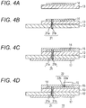
- Figs. 4A to 4D are schematic cross-sectional views for describing the steps of manufacturing the stretchable circuit board 11.
- the conductor layer 14 is formed on one surface (the upper surface) of the non-stretchable substrate 13.
- the non-stretchable substrate 13 is bonded to the partial region of one surface (the upper surface) of the stretchable substrate 12.
- the through-hole 21a penetrating the conductor layer 14, the non-stretchable substrate 13, and the stretchable substrate 12 is formed.
- the conductive paste 21b is embedded in the through-hole 21a.
- the first via 21 is formed.
- the insulating layer 15 covering the conductor layer 14 is formed on one surface (the upper surface) of the non-stretchable substrate 13.
- the stretchable wiring 17 is formed on the other surface (the lower surface) of the stretchable substrate 12.
- the conductive composition (the conductive paste) as the material of the stretchable wiring 17 is screen-printed on the lower surface of the stretchable substrate 12.
- the conductive paste is dried, and in this manner, the stretchable wiring 17 is formed on the lower surface of the stretchable substrate 12.
- the stretchable wiring 17 may be formed in such a manner that the conductive composition (the conductive paste) as the material of the stretchable wiring 17 is dried after having been applied to the lower surface of the stretchable substrate 12 by a dispenser.
- the stretchable wiring 17 may be formed in such a manner that the stretchable wiring 17 is formed on a not-shown releasing film by, e.g., screen printing and then the stretchable wiring 17 is thermally transferred onto the stretchable substrate 12.
- the stretchable wiring 17 is in such a state that the stretchable wiring 17 is connected to the conductor layer 14 through the first via 21.
- the through-hole 22a is formed to penetrate the insulating layer 15 to the conductor layer 14. Subsequently, the conductive paste 22b is embedded in the through-hole 22a. Thus, the second via 22 is formed. Finally, the electronic component 16 is mounted on the insulating layer 15 with the electronic component 16 being electrically connected to the second via 22.
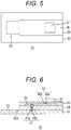
- Fig. 5 is a schematic plan view of a stretchable circuit board of a third embodiment of the present invention.
- Fig. 6 is a schematic cross-sectional view of the stretchable circuit board of Fig. 5 .
- a stretchable circuit board 31 includes a stretchable substrate 32 exhibiting elasticity and formed in a rectangular shape elongated in one direction (a right-to-left direction in Fig. 5 ) as viewed in the plane.
- the stretchable substrate 32 is made of a material exhibiting elasticity.
- elastomer e.g., polyurethane elastomer, styrene elastomer, olefin elastomer, polyamide elastomer, and silicone elastomer
- synthetic rubber e.g., ethylene-propylene rubber, nitrile-butadiene rubber, silicone rubber, acrylic rubber, fluorine rubber, and urethane rubber
- a stretchable wiring 33 exhibiting elasticity is formed on a partial region of one surface (an upper surface in Fig. 6 ) of the stretchable substrate 32. Specifically, a recessed portion 32a is formed at one surface (the upper surface) of the stretchable substrate 32. The stretchable wiring 33 is formed in the recessed portion 32a.
- the stretchable wiring 33 is made of a conductive composition containing elastomer and a conductive filler filling the elastomer.
- the conductive filler may include a coil-shaped conductive filler as described above.
- the conductive filler may include a dendrite-shaped conductive filler as described above.
- the conductive filler may include both of the coil-shaped conductive filler and the dendrite-shaped conductive filler as described above.
- a non-stretchable substrate 34 not exhibiting elasticity and formed in a rectangular shape elongated in one direction (the right-to-left direction in Fig. 5 ) as viewed in the plane is bonded and fixed to a partial region of one surface (the upper surface) of the stretchable substrate 32, the partial region including at least a portion of the stretchable wiring 33.
- the length and width of the non-stretchable substrate 34 are shorter than those of the stretchable substrate 32.
- the non-stretchable substrate 34 is bonded to the stretchable substrate 32 in such a posture that as viewed in the plane, one end of the non-stretchable substrate 34 is coincident with one end of the stretchable substrate 32 and a center line passing through the center of the non-stretchable substrate 34 in a width direction thereof is coincident with a center line passing through the center of the stretchable substrate 32 in a width direction thereof.
- a conductor layer 35 is formed on the surface (an upper surface in Fig. 6 ) of the non-stretchable substrate 34 opposite to the surface bonded to the stretchable substrate 32.
- a rigid substrate or a flexible substrate is used as the non-stretchable substrate 34.
- a glass epoxy substrate, a bismaleimide substrate, a copper clad laminate (CCL), etc. are used as the non-stretchable substrate 34.
- the copper clad laminate (CCL) is configured such that copper foil is bonded to one or both surfaces of an insulating film made of polyimide etc.
- the conductor layer 35 can be formed of the copper foil of the copper clad laminate (CCL).
- An insulating layer 36 covering the conductor layer 35 is formed on the upper surface of the non-stretchable substrate 34.
- polyimide, epoxy, glass epoxy, or bismaleimide is used as the insulating layer 36.
- An electronic component 37 such as a semiconductor element is mounted on a surface (an upper surface in Fig. 6 ) of the insulating layer 36.
- the conductor layer 35 and the stretchable wiring 33 are electrically connected together through a first via 41 penetrating the non-stretchable substrate 34.
- the first via 41 includes a through-hole 41a penetrating the conductor layer 35 and the non-stretchable substrate 34; and conductive paste 41b embedded in the through-hole 41a.
- the first via 41 may include a through-hole penetrating the conductor layer 35 and the non-stretchable substrate 34; and a metal layer (e.g., copper) formed on an inner surface of the through-hole by plating.
- the electronic component 37 and the conductor layer 35 are electrically connected together through a second via 42 penetrating the insulating layer 36.
- the second via 42 includes, for example, a through-hole 42a penetrating the insulating layer 36, and conductive paste 42b embedded in the through-hole 42a.
- the second via 42 may include a through-hole penetrating the insulating layer 36, and a metal layer (e.g., copper) formed on an inner surface of the through-hole by plating.
- the electronic component 37 is electrically connected to the stretchable wiring 33 through the second via 42, the conductor layer 35, and the first via 41.
- the stretchable wiring 33 exhibiting elasticity is formed on the partial region of one surface (the upper surface) of the stretchable substrate 32 exhibiting elasticity.
- the non-stretchable substrate 34 not exhibiting elasticity is bonded to the partial region of one surface (the upper surface) of the stretchable substrate 32, the partial region including at least a portion of the stretchable wiring 33.
- the stretchable substrate 32 and the stretchable wiring 33 hold elasticity in a region to which the non-stretchable substrate 34 is not bonded.
- the stretchable circuit board 31 exhibiting elasticity is obtained.
- Figs. 7A to 7D are schematic cross-sectional views for describing the steps of manufacturing the stretchable circuit board 31.
- the conductor layer 35 is formed on one surface (the upper surface) of the non-stretchable substrate 34.
- the through-hole 41a penetrating the conductor layer 35 and the non-stretchable substrate 34 is formed.
- the conductive paste 41b is embedded in the through-hole 41a.
- the first via 41 is formed.
- the insulating layer 36 covering the conductor layer 35 is formed on one surface (the upper surface) of the non-stretchable substrate 34. In this manner, the non-stretchable substrate 34 having the conductor layer 35, the insulating layer 36, and the first via 41 is produced.
- the recessed portion 32a is formed at one surface (the upper surface) of the stretchable substrate 32.
- the stretchable wiring 33 is formed in the recessed portion 32a.
- a method similar to the method for forming the stretchable wiring 17 of the stretchable wiring board 11 according to the second embodiment can be used as the method for forming the stretchable wiring 33. In this manner, the stretchable substrate 32 configured such that the stretchable wiring 33 is formed on a portion of one surface is produced.
- the non-stretchable substrate 34 is bonded to the partial region of one surface (the upper surface) of the stretchable substrate 32, the partial region including at least a portion of the stretchable wiring 33.
- the non-stretchable substrate 34 having the conductor layer 35, the insulating layer 36, and the first via 41 is bonded to the stretchable substrate 32 provided with the stretchable wiring 33.
- the through-hole 42a is formed to penetrate the insulating layer 36 to the conductor layer 35.
- the conductive paste 42b is embedded in the through-hole 42a.
- the second via 42 is formed.
- the electronic component 37 is mounted on the insulating layer 36 with the electronic component 37 being electrically connected to the second via 42.
- Fig. 8 is a schematic plan view of a stretchable circuit board of a fourth embodiment of the present invention.
- Fig. 9 is a schematic cross-sectional view of the stretchable circuit board of Fig. 8 .
- the same reference numerals as those of Figs. 5 and 6 are used to represent elements corresponding to the elements of Figs. 5 and 6 .
- a stretchable circuit board 51 includes a stretchable substrate 32.
- a recessed portion 32a is formed at one surface (an upper surface in Fig. 9 ) of the stretchable substrate 32.
- a stretchable wiring 33 is formed in the recessed portion 32a.
- a non-stretchable substrate 34 is bonded and fixed to a partial region of one surface (the upper surface) of the stretchable substrate 32, the partial region including at least a portion of the stretchable wiring 33.
- the non-stretchable substrate 34 has an extension 34a. The extension 34a extends outward from one end of the stretchable substrate 32.
- a conductor layer 35 is formed on the surface (an upper surface in Fig. 9 ) of the non-stretchable substrate 34 opposite to the surface bonded to the stretchable substrate 32.
- the conductor layer 35 has an extension 35a formed on the extension 34a of the non-stretchable substrate 34.
- An insulating layer 36 covering the conductor layer 35 is formed on the upper surface of the non-stretchable substrate 34.
- the insulating layer 36 has an extension 36a covering the extension 35a of the conductor layer 35 and the extension 34a of the non-stretchable substrate 34.
- An electronic component 37 such as a semiconductor element is mounted on a surface (an upper surface in Fig. 9 ) of the extension 36a of the insulating layer 36.
- the conductor layer 35 and the stretchable wiring 33 are electrically connected together through a first via 41 penetrating the non-stretchable substrate 34.
- the electronic component 37 and the extension 35a of the conductor layer 35 are electrically connected together through a second via 42 penetrating the extension 36a of the insulating layer 36.
- the method for manufacturing the stretchable circuit board 51 of the fourth embodiment is similar to the method for manufacturing the stretchable circuit board 31 of the third embodiment as described above, and therefore, description thereof will not be repeated.
- the electronic component 16, 37 is electrically connected to the conductor layer 14, 35 through the via 22, 42.
- the electronic component 16, 37 may be directly joined to the conductor layer 14, 35 by a joint member such as solder.
- stretchable cable of the above-described first embodiment and the stretchable circuit boards of the above-described second to fourth embodiments include, for example, an electrocardiographic or myoelectric biosignal measurement sensor, a strain sensor, and a piezoelectric element electrode.
Landscapes
- Engineering & Computer Science (AREA)
- Microelectronics & Electronic Packaging (AREA)
- Manufacturing & Machinery (AREA)
- Chemical & Material Sciences (AREA)
- Dispersion Chemistry (AREA)
- Physics & Mathematics (AREA)
- Spectroscopy & Molecular Physics (AREA)
- Structure Of Printed Boards (AREA)
- Parts Printed On Printed Circuit Boards (AREA)
- Insulated Conductors (AREA)
- Laminated Bodies (AREA)
- Production Of Multi-Layered Print Wiring Board (AREA)
Abstract
Description
- The present invention relates to a stretchable cable exhibiting elasticity and a stretchable circuit board exhibiting elasticity.
- A flexible printed circuit (FPC) board exhibits bendability, whereas does not exhibit elasticity. Thus, a circuit board has been known, which is configured such that a rigid substrate is stacked on a FPC etched in a wave shape (an accordion shape). However, in this circuit board, the FPC can deform by twisting, but the FPC itself is not stretchable.
- Patent Literature 1:
JP-T-2009-533839 - The present invention is intended to provide a stretchable cable exhibiting elasticity.
- The present invention is intended to provide a stretchable circuit board exhibiting elasticity.
- A stretchable cable according to the present invention includes a sheet-shaped base material exhibiting elasticity, and a wiring formed on one surface of the base material and exhibiting elasticity. The wiring is made of a conductive composition containing elastomer and a conductive filler filling the elastomer.
- In this configuration, the base material and the wiring exhibit elasticity. Thus, the stretchable cable exhibiting elasticity is obtained.
- In one embodiment of the present invention, the conductive filler includes a coil-shaped conductive filler.
- The coil-shaped conductive filler may be, for example, a small metal coil manufactured in such a manner that metal plating is applied to a natural helical structure. The coil-shaped conductive filler may be a small metal spring manufactured in such a manner that a metal wire is processed into a coil shape. The coil-shaped conductive filler may be a carbon nanocoil.
- In this configuration, the conductive filler includes the coil-shaped conductive filler. Thus, when the elastomer in the conductive composition stretches, the conductive filler in the conductive composition stretches as in a pulled coil. Accordingly, even when the elastomer stretches, an increase in a resistance value of the wiring can be suppressed. As a result, the stretchable cable can be realized, which has the wiring exhibiting elasticity and configured so that an increase in the resistance value in stretching can be suppressed.
- In one embodiment of the present invention, the conductive filler includes a dendrite-shaped conductive filler.
- The dendrite shape indicates such a shape that a rod-shaped bifurcated branch extends from a rod-shaped main branch in a two-dimensional direction or a three-dimensional direction. Moreover, the dendrite shape also includes a shape in which the bifurcated branch bends in the middle, and a shape in which a rod-shaped bifurcated branch further extends from the middle of the bifurcated branch.
- In this configuration, the conductive filler includes the dendrite-shaped conductive filler. Even when the elastomer in the conductive composition is stretched, the probability of contacting the conductive fillers of the conductive composition each other can be improved. Thus, even in the case of stretching the elastomer, a conductive path can be satisfactorily formed in the elastomer. As a result, the stretchable cable can be realized, which has the wiring exhibiting elasticity and configured so that an increase in the resistance value in stretching can be suppressed.
- A first stretchable circuit board according to the present invention includes a stretchable substrate exhibiting elasticity, a non-stretchable substrate bonded to a partial region of one surface of the stretchable substrate and not exhibiting elasticity, and a stretchable wiring formed on the other surface of the stretchable substrate and exhibiting elasticity.
- In this configuration, the non-stretchable substrate not exhibiting elasticity is bonded to the partial region of one surface of the stretchable substrate exhibiting elasticity. An electronic component not exhibiting elasticity can be mounted on this non-stretchable substrate side. The stretchable wiring exhibiting elasticity is formed on the other surface of the stretchable substrate. The stretchable substrate and the stretchable wiring hold elasticity in a region to which the non-stretchable substrate is not bonded. Thus, the stretchable circuit board exhibiting elasticity is obtained.
- In one embodiment of the present invention, a conductor layer formed on the surface of the non-stretchable substrate opposite to the surface bonded to the stretchable substrate and a first via penetrating the stretchable substrate and the non-stretchable substrate and connecting the stretchable wiring and the conductor layer together are provided. In this configuration, the electronic component mounted on the non-stretchable substrate side can be connected to the stretchable wiring through the conductor layer and the first via.
- In one embodiment of the present invention, an insulating layer covering the conductor layer, an electronic component provided on a surface of the insulating layer, and a second via penetrating the insulating layer and electrically connecting the conductor layer and the electronic component together are provided. In this configuration, the electronic component can be connected to the stretchable wiring through the second via, the conductor layer, and the first via.
- A second stretchable circuit board according to the present invention includes a stretchable substrate exhibiting elasticity, a stretchable wiring formed on a portion of one surface of the stretchable substrate and exhibiting elasticity, and a non-stretchable substrate not exhibiting elasticity and bonded to a partial region of one surface of the stretchable substrate, the partial region including at least a portion of the stretchable wiring.
- In this configuration, the stretchable wiring exhibiting elasticity is formed in the partial region of one surface of the stretchable substrate exhibiting elasticity. The non-stretchable substrate not exhibiting elasticity is bonded to the partial region of one surface of the stretchable substrate, the partial region including at least a portion of the stretchable wiring. An electronic component not exhibiting elasticity can be mounted on this non-stretchable substrate side. The stretchable substrate and the stretchable wiring hold elasticity in a region to which the non-stretchable substrate is not bonded. Thus, the stretchable circuit board exhibiting elasticity is obtained.
- In one embodiment of the present invention, a conductor layer formed on the surface of the non-stretchable substrate opposite to the surface bonded to the stretchable substrate and a first via penetrating the non-stretchable substrate and connecting the stretchable wiring and the conductor layer together are further provided. In this configuration, the electronic component mounted on the non-stretchable substrate side can be connected to the stretchable wiring through the conductor layer and the first via.
- In one embodiment of the present invention, an insulating layer covering the conductor layer, an electronic component provided on a surface of the insulating layer, and a second via penetrating the insulating layer and electrically connecting the conductor layer and the electronic component together are further provided. In this configuration, the electronic component can be connected to the stretchable wiring through the second via, the conductor layer, and the first via.
- In one embodiment of the present invention, the non-stretchable substrate is a rigid substrate or a flexible substrate.
-
-
Fig. 1 is a schematic cross-sectional view of a configuration of a stretchable cable of a first embodiment of the present invention. -
Fig. 2 is a schematic plan view of a stretchable circuit board of a second embodiment of the present invention. -
Fig. 3 is a schematic cross-sectional view of the stretchable circuit board ofFig. 2 . -
Figs. 4A to 4D are schematic cross-sectional views for describing the steps of manufacturing the stretchable circuit board ofFig. 2 . -
Fig. 5 is a schematic plan view of a stretchable circuit board of a third embodiment of the present invention. -
Fig. 6 is a schematic cross-sectional view of the stretchable circuit board ofFig. 5 . -
Figs. 7A to 7D are schematic cross-sectional views for describing the steps of manufacturing the stretchable circuit board ofFig. 5 . -
Fig. 8 is a schematic plan view of a stretchable circuit board of a fourth embodiment of the present invention. -
Fig. 9 is a schematic cross-sectional view of the stretchable circuit board ofFig. 8 . - Embodiments of the present invention will be described below in detail with reference to the attached drawings.
-
Fig. 1 is a schematic cross-sectional view of a configuration of a stretchable cable of a first embodiment of the present invention. - A
stretchable cable 1 includes a sheet-shapedstretchable base material 2 exhibiting elasticity and elongated in one direction (a right-to-left direction inFig. 1 ), and astretchable wiring 3 formed on one surface of thestretchable base material 2 and exhibiting elasticity. Thestretchable wiring 3 includes a plurality ofstretchable wires 3a. Thestretchable wires 3a extend in parallel to each other at intervals in a width direction of thestretchable base material 2. - The
stretchable base material 2 is made of a material exhibiting elasticity. For example, elastomer (e.g., polyurethane elastomer, styrene elastomer, olefin elastomer, polyamide elastomer, and silicone elastomer) or synthetic rubber (e.g., ethylene-propylene rubber, nitrile-butadiene rubber, silicone rubber, acrylic rubber, fluorine rubber, and urethane rubber) can be used as the material forming thestretchable base material 2. - The
stretchable wiring 3 is made of a conductive composition including elastomer and a conductive filler filling the elastomer. The shape of the conductive filler may be a coil shape, a dendrite shape, a block shape, a spherical shape, a flake shape, a needle shape, and a fiber shape. - In this embodiment, the conductive filler includes a conductive filler in the coil shape (hereinafter referred to as a "coil-shaped conductive filler"). The coil shape includes a helical shape and a spiral shape. In this embodiment, the conductive filler is in the coil shape. Thus, when the elastomer stretches, the coil-shaped conductive filler stretches as in a pulled coil. Thus, even when the elastomer stretches, an increase in a resistance value of the
stretchable wiring 3 can be suppressed. Thus, thestretchable cable 1 can be realized, which has thestretchable wiring 3 exhibiting elasticity and configured so that an increase in the resistance value in stretching can be suppressed. - The elastomer is resin having elastic force, such as styrene elastomer, olefin elastomer, polyester elastomer, polyurethane elastomer, polyamide elastomer, and silicone elastomer. The polyurethane elastomer includes a hard segment and a soft segment. The soft segment includes, for example, carbonate, ester, and ether. Specifically, NE-8880, MAU-9022, NE-310, NE-302HV, and CU-8448 etc. manufactured by Dainichiseika Color and Chemicals Mfg. Co., Ltd. can be used. The elastomer may be made of a single type of resin or multiple types of resin. Considering improvement of manufacturability (workability), flexibility, etc., the elastomer may contain an additive such as a plasticizing agent, a processing aid, a cross-linking agent, a vulcanization accelerator, a vulcanization aid, an anti-aging agent, a softening agent, and a coloring agent.
- The filling rate of the coil-shaped conductive filler in the conductive composition is preferably equal to or greater than 30% by weight and equal to or less than 95% by weight.
- The coil-shaped conductive filler may be a small metal coil manufactured in such a manner that metal plating is applied to a natural helical structure. Such a small metal coil is manufactured in such a manner that metal plating is applied to a small helical structure in plants and algae. For example, the small metal coil is obtained in such a manner that metal plating is applied to alga spirulina. The alga spirulina has a coil shape. After the spirulina has been cultivated and immobilized, metal plating (non-electrolytic plating) is applied to the spirulina. Metal exhibiting conductivity, such as copper, silver, and gold is used as a metal plating material.
- Moreover, the coil-shaped conductive filler may be a small metal spring manufactured in such a manner that a metal wire is processed into a coil shape. Specifically, a wire rod having a conductor diameter (a wire diameter) of equal to or smaller than 30 µm is processed into a coil shape, and in this manner, a small metal spring is obtained. An extremely-thin wire made of metal exhibiting conductivity, such as copper or silver or the above-described extremely-thin metal-plated wire is used as the wire rod.
- Further, the coil-shaped conductive filler may be a carbon nanocoil (CNC). The carbon nanocoil indicates a carbon nanofiber (CNF) grown in a helical shape. The carbon nanofiber is a fibrous material made of carbon.
- The conductor diameter (the wire diameter) of the coil-shaped conductive filler is preferably equal to or greater than 5 µm and equal to or smaller than 30 µm. The coil outer diameter of the coil-shaped conductive filler is preferably equal to or smaller than 150 µm. The pitch of the coil-shaped conductive filler is preferably equal to or greater than 10 µm and equal to or smaller than 150 µm. The coil length of the coil-shaped conductive filler is preferably equal to or smaller than 1 mm, and more preferably equal to or smaller than 500 µm.
- Note that in addition to the above-described coil-shaped conductive filler, a block-shaped, spherical-shaped, flake-shaped, needle-shaped, or fiber-shaped conductive filler may be used as the conductive filler, for example.
- Instead of or in addition to the coil-shaped conductive filler, the conductive filler may include a dendrite-shaped conductive filler. In the case of containing the dendrite-shaped conductive filler in the conductive filler, even when the elastomer is stretched, the probability of contacting the conductive fillers each other can be improved. Thus, even in the case of stretching the elastomer, a conductive path can be satisfactorily formed in the elastomer. As a result, the stretchable cable can be realized, which has the
stretchable wiring 3 exhibiting elasticity and configured so that an increase in the resistance value in stretching can be suppressed. - The dendrite shape indicates such a shape that a rod-shaped bifurcated branch extends from a rod-shaped main branch in a two-dimensional direction or a three-dimensional direction. Moreover, the dendrite shape also includes a shape in which the bifurcated branch bends in the middle, and a shape in which a rod-shaped bifurcated branch further extends from the middle of the bifurcated branch.
- The dendrite-shaped conductive filler may be, for example, such silver-coated copper powder that dendrite-shaped copper powder is coated with silver. Moreover, the dendrite-shaped conductive filler may be, for example, dendrite-shaped copper powder or silver powder. In a case where the conductive filler is made of the dendrite-shaped silver-coated copper powder, the conductive filler can be realized, which is available at relatively-low cost while having a resistance value close to that of the conductive filler made of silver and which exhibits excellent conductivity and migration resistance. In a case where the conductive filler is made of the dendrite-shaped copper powder, the conductive filler can be realized, which is available at low cost while having a low resistance value. The dendrite-shaped conductive filler may be such gold-coated copper powder that dendrite-shaped copper powder is coated with other conductive materials than silver, such as gold.
- The lower limit of the particle size of the dendrite-shaped conductive filler is 1 µm, and preferably 2 µm. When the lower limit is equal to or greater than 1 µm, the conductive fillers can easily contact each other, leading to satisfactory conductivity of the
stretchable wiring 3. Moreover, the upper limit of the particle size of the conductive filler is 20 µm, and preferably 10 µm. When the upper limit is equal to or smaller than 20 µm, the thickness of thestretchable wiring 3 can be decreased. - In the
stretchable cable 1 of the first embodiment, thestretchable base material 2 and thestretchable wiring 3 exhibit elasticity. Thus, the stretchable cable exhibiting elasticity is obtained. - The
stretchable cable 1 illustrated inFig. 1 is manufactured as follows, for example. That is, the conductive composition (conductive paste) as the material of thestretchable wiring 3 is screen-printed on one surface of thestretchable base material 2. Then, the conductive paste is dried, and in this manner, thestretchable wiring 3 is formed on one surface of thestretchable base material 2. - Note that the
stretchable wiring 3 may be formed in such a manner that the conductive composition (the conductive paste) as the material of thestretchable wiring 3 is dried after having been applied to one surface of thestretchable base material 2 by a dispenser. - Alternatively, the
stretchable wiring 3 may be formed in such a manner that thestretchable wiring 3 is formed on a not-shown releasing film by, e.g., screen printing and then thestretchable wiring 3 is thermally transferred onto thestretchable base material 2. -
Fig. 2 is a schematic plan view of a stretchable circuit board of a second embodiment of the present invention.Fig. 3 is a schematic cross-sectional view of the stretchable circuit board ofFig. 2 . - A
stretchable circuit board 11 includes astretchable substrate 12 exhibiting elasticity and formed in a rectangular shape elongated in one direction (a right-to-left direction inFig. 2 ) as viewed in the plane. Thestretchable substrate 12 is made of a material exhibiting elasticity. For example, elastomer (e.g., polyurethane elastomer, styrene elastomer, olefin elastomer, polyamide elastomer, and silicone elastomer) or synthetic rubber (e.g., ethylene-propylene rubber, nitrile-butadiene rubber, silicone rubber, acrylic rubber, fluorine rubber, and urethane rubber) can be used as the material forming thestretchable substrate 12. - A
non-stretchable substrate 13 not exhibiting elasticity and formed in a rectangular shape elongated in one direction (the right-to-left direction inFig. 2 ) as viewed in the plane is bonded and fixed to a partial region of one surface (an upper surface inFig. 3 ) of thestretchable substrate 12. In this embodiment, the length and width of thenon-stretchable substrate 13 are shorter than those of thestretchable substrate 12. Moreover, in this embodiment, thenon-stretchable substrate 13 is bonded to thestretchable substrate 12 in such a posture that as viewed in the plane, one end of thenon-stretchable substrate 13 is coincident with one end of thestretchable substrate 12 and a center line passing through the center of thenon-stretchable substrate 13 in a width direction thereof is coincident with a center line passing through the center of thestretchable substrate 12 in a width direction thereof. Aconductor layer 14 is formed on the surface (an upper surface inFig. 3 ) of thenon-stretchable substrate 13 opposite to the surface bonded to thestretchable substrate 12. - A rigid substrate or a flexible substrate is used as the
non-stretchable substrate 13. Specifically, a glass epoxy substrate, a bismaleimide substrate, a copper clad laminate (CCL), etc. are used as thenon-stretchable substrate 13. The copper clad laminate (CCL) is configured such that copper foil is bonded to one or both surfaces of an insulating film made of polyimide etc. In the case of using the copper clad laminate (CCL) as thenon-stretchable substrate 13, theconductor layer 14 can be formed of the copper foil of the copper clad laminate (CCL). - An insulating
layer 15 covering theconductor layer 14 is formed on the upper surface of thenon-stretchable substrate 13. For example, polyimide, epoxy, glass epoxy, or bismaleimide is used as the insulatinglayer 15. Anelectronic component 16 such as a semiconductor element is mounted on a surface (an upper surface inFig. 3 ) of the insulatinglayer 15. The semiconductor element includes, for example, a transistor, an integrated circuit (IC, LSI), a resistor, and a capacitor. - A
stretchable wiring 17 exhibiting elasticity is formed on the other surface (a lower surface inFig. 3 ) of thestretchable substrate 12. Thestretchable wiring 17 is made of a conductive composition containing elastomer and a conductive filler filling the elastomer. The conductive filler may include a coil-shaped conductive filler as described above. Alternatively, the conductive filler may include a dendrite-shaped conductive filler as described above. As another alternative, the conductive filler may include both of the coil-shaped conductive filler and the dendrite-shaped conductive filler as described above. - The
conductor layer 14 and thestretchable wiring 17 are electrically connected together through a first via 21 penetrating thenon-stretchable substrate 13 and thestretchable substrate 12. For example, the first via 21 includes a through-hole 21a penetrating theconductor layer 14, thenon-stretchable substrate 13, and thestretchable substrate 12; andconductive paste 21b embedded in the through-hole 21a. Theconductive paste 21b may be, for example, epoxy resin filled with the conductive filler such as silver-coated copper powder, silver, and copper. Theconductive paste 21b may be, for example, paste described in Japanese Patent No.4191678 4468750 4437946 4949802 conductor layer 14, thenon-stretchable substrate 13, and thestretchable substrate 12; and a metal layer (e.g., copper) formed on an inner surface of the through-hole by plating. - The
electronic component 16 and theconductor layer 14 are electrically connected together through a second via 22 penetrating the insulatinglayer 15. The second via 22 includes, for example, a through-hole 22a penetrating the insulatinglayer 15, andconductive paste 22b embedded in the through-hole 22a. The second via 22 may include a through-hole penetrating the insulatinglayer 15, and a metal layer (e.g., copper) formed on an inner surface of the through-hole by plating. Theelectronic component 16 is electrically connected to thestretchable wiring 17 through the second via 22, theconductor layer 14, and the first via 21. - In this
stretchable circuit board 11, thenon-stretchable substrate 13 not exhibiting elasticity is bonded to a partial region of one surface (the upper surface) of thestretchable substrate 12 exhibiting elasticity. Thestretchable wiring 17 exhibiting elasticity is formed on the other surface (the lower surface) of thestretchable substrate 12. Thestretchable substrate 12 and thestretchable wiring 17 hold elasticity in a region to which thenon-stretchable substrate 13 is not bonded. Thus, the stretchable circuit board exhibiting elasticity is obtained. -
Figs. 4A to 4D are schematic cross-sectional views for describing the steps of manufacturing thestretchable circuit board 11. First, as illustrated inFig. 4A , theconductor layer 14 is formed on one surface (the upper surface) of thenon-stretchable substrate 13. Next, as illustrated inFig. 4B , thenon-stretchable substrate 13 is bonded to the partial region of one surface (the upper surface) of thestretchable substrate 12. Next, the through-hole 21a penetrating theconductor layer 14, thenon-stretchable substrate 13, and thestretchable substrate 12 is formed. Subsequently, theconductive paste 21b is embedded in the through-hole 21a. Thus, the first via 21 is formed. - Next, as illustrated in
Fig. 4C , the insulatinglayer 15 covering theconductor layer 14 is formed on one surface (the upper surface) of thenon-stretchable substrate 13. Subsequently, thestretchable wiring 17 is formed on the other surface (the lower surface) of thestretchable substrate 12. Specifically, the conductive composition (the conductive paste) as the material of thestretchable wiring 17 is screen-printed on the lower surface of thestretchable substrate 12. Then, the conductive paste is dried, and in this manner, thestretchable wiring 17 is formed on the lower surface of thestretchable substrate 12. Note that thestretchable wiring 17 may be formed in such a manner that the conductive composition (the conductive paste) as the material of thestretchable wiring 17 is dried after having been applied to the lower surface of thestretchable substrate 12 by a dispenser. Alternatively, thestretchable wiring 17 may be formed in such a manner that thestretchable wiring 17 is formed on a not-shown releasing film by, e.g., screen printing and then thestretchable wiring 17 is thermally transferred onto thestretchable substrate 12. Thestretchable wiring 17 is in such a state that thestretchable wiring 17 is connected to theconductor layer 14 through the first via 21. - Next, as illustrated in
Fig. 4D , the through-hole 22a is formed to penetrate the insulatinglayer 15 to theconductor layer 14. Subsequently, theconductive paste 22b is embedded in the through-hole 22a. Thus, the second via 22 is formed. Finally, theelectronic component 16 is mounted on the insulatinglayer 15 with theelectronic component 16 being electrically connected to the second via 22. -
Fig. 5 is a schematic plan view of a stretchable circuit board of a third embodiment of the present invention.Fig. 6 is a schematic cross-sectional view of the stretchable circuit board ofFig. 5 . - A
stretchable circuit board 31 includes astretchable substrate 32 exhibiting elasticity and formed in a rectangular shape elongated in one direction (a right-to-left direction inFig. 5 ) as viewed in the plane. Thestretchable substrate 32 is made of a material exhibiting elasticity. For example, elastomer (e.g., polyurethane elastomer, styrene elastomer, olefin elastomer, polyamide elastomer, and silicone elastomer) or synthetic rubber (e.g., ethylene-propylene rubber, nitrile-butadiene rubber, silicone rubber, acrylic rubber, fluorine rubber, and urethane rubber) can be used as the material forming thestretchable substrate 32. - A
stretchable wiring 33 exhibiting elasticity is formed on a partial region of one surface (an upper surface inFig. 6 ) of thestretchable substrate 32. Specifically, a recessedportion 32a is formed at one surface (the upper surface) of thestretchable substrate 32. Thestretchable wiring 33 is formed in the recessedportion 32a. Thestretchable wiring 33 is made of a conductive composition containing elastomer and a conductive filler filling the elastomer. The conductive filler may include a coil-shaped conductive filler as described above. Alternatively, the conductive filler may include a dendrite-shaped conductive filler as described above. As another alternative, the conductive filler may include both of the coil-shaped conductive filler and the dendrite-shaped conductive filler as described above. - A
non-stretchable substrate 34 not exhibiting elasticity and formed in a rectangular shape elongated in one direction (the right-to-left direction inFig. 5 ) as viewed in the plane is bonded and fixed to a partial region of one surface (the upper surface) of thestretchable substrate 32, the partial region including at least a portion of thestretchable wiring 33. In this embodiment, the length and width of thenon-stretchable substrate 34 are shorter than those of thestretchable substrate 32. Moreover, in this embodiment, thenon-stretchable substrate 34 is bonded to thestretchable substrate 32 in such a posture that as viewed in the plane, one end of thenon-stretchable substrate 34 is coincident with one end of thestretchable substrate 32 and a center line passing through the center of thenon-stretchable substrate 34 in a width direction thereof is coincident with a center line passing through the center of thestretchable substrate 32 in a width direction thereof. Aconductor layer 35 is formed on the surface (an upper surface inFig. 6 ) of thenon-stretchable substrate 34 opposite to the surface bonded to thestretchable substrate 32. - A rigid substrate or a flexible substrate is used as the
non-stretchable substrate 34. Specifically, a glass epoxy substrate, a bismaleimide substrate, a copper clad laminate (CCL), etc. are used as thenon-stretchable substrate 34. The copper clad laminate (CCL) is configured such that copper foil is bonded to one or both surfaces of an insulating film made of polyimide etc. In the case of using the copper clad laminate (CCL) as thenon-stretchable substrate 34, theconductor layer 35 can be formed of the copper foil of the copper clad laminate (CCL). - An insulating
layer 36 covering theconductor layer 35 is formed on the upper surface of thenon-stretchable substrate 34. For example, polyimide, epoxy, glass epoxy, or bismaleimide is used as the insulatinglayer 36. Anelectronic component 37 such as a semiconductor element is mounted on a surface (an upper surface inFig. 6 ) of the insulatinglayer 36. - The
conductor layer 35 and thestretchable wiring 33 are electrically connected together through a first via 41 penetrating thenon-stretchable substrate 34. For example, the first via 41 includes a through-hole 41a penetrating theconductor layer 35 and thenon-stretchable substrate 34; andconductive paste 41b embedded in the through-hole 41a. The first via 41 may include a through-hole penetrating theconductor layer 35 and thenon-stretchable substrate 34; and a metal layer (e.g., copper) formed on an inner surface of the through-hole by plating. - The
electronic component 37 and theconductor layer 35 are electrically connected together through a second via 42 penetrating the insulatinglayer 36. The second via 42 includes, for example, a through-hole 42a penetrating the insulatinglayer 36, andconductive paste 42b embedded in the through-hole 42a. The second via 42 may include a through-hole penetrating the insulatinglayer 36, and a metal layer (e.g., copper) formed on an inner surface of the through-hole by plating. Theelectronic component 37 is electrically connected to thestretchable wiring 33 through the second via 42, theconductor layer 35, and the first via 41. - In this
stretchable circuit board 31, thestretchable wiring 33 exhibiting elasticity is formed on the partial region of one surface (the upper surface) of thestretchable substrate 32 exhibiting elasticity. Thenon-stretchable substrate 34 not exhibiting elasticity is bonded to the partial region of one surface (the upper surface) of thestretchable substrate 32, the partial region including at least a portion of thestretchable wiring 33. Thestretchable substrate 32 and thestretchable wiring 33 hold elasticity in a region to which thenon-stretchable substrate 34 is not bonded. Thus, thestretchable circuit board 31 exhibiting elasticity is obtained. -
Figs. 7A to 7D are schematic cross-sectional views for describing the steps of manufacturing thestretchable circuit board 31. First, as illustrated inFig. 7A , theconductor layer 35 is formed on one surface (the upper surface) of thenon-stretchable substrate 34. Next, the through-hole 41a penetrating theconductor layer 35 and thenon-stretchable substrate 34 is formed. Next, theconductive paste 41b is embedded in the through-hole 41a. Thus, the first via 41 is formed. Subsequently, the insulatinglayer 36 covering theconductor layer 35 is formed on one surface (the upper surface) of thenon-stretchable substrate 34. In this manner, thenon-stretchable substrate 34 having theconductor layer 35, the insulatinglayer 36, and the first via 41 is produced. - Meanwhile, as illustrated in
Fig. 7B , the recessedportion 32a is formed at one surface (the upper surface) of thestretchable substrate 32. Thestretchable wiring 33 is formed in the recessedportion 32a. A method similar to the method for forming thestretchable wiring 17 of thestretchable wiring board 11 according to the second embodiment can be used as the method for forming thestretchable wiring 33. In this manner, thestretchable substrate 32 configured such that thestretchable wiring 33 is formed on a portion of one surface is produced. - Next, as illustrated in
Fig. 7C , thenon-stretchable substrate 34 is bonded to the partial region of one surface (the upper surface) of thestretchable substrate 32, the partial region including at least a portion of thestretchable wiring 33. Thus, thenon-stretchable substrate 34 having theconductor layer 35, the insulatinglayer 36, and the first via 41 is bonded to thestretchable substrate 32 provided with thestretchable wiring 33. - Next, as illustrated in
Fig. 7D , the through-hole 42a is formed to penetrate the insulatinglayer 36 to theconductor layer 35. Subsequently, theconductive paste 42b is embedded in the through-hole 42a. Thus, the second via 42 is formed. Finally, theelectronic component 37 is mounted on the insulatinglayer 36 with theelectronic component 37 being electrically connected to the second via 42. -
Fig. 8 is a schematic plan view of a stretchable circuit board of a fourth embodiment of the present invention.Fig. 9 is a schematic cross-sectional view of the stretchable circuit board ofFig. 8 . InFigs. 8 and 9 , the same reference numerals as those ofFigs. 5 and 6 are used to represent elements corresponding to the elements ofFigs. 5 and 6 . - A
stretchable circuit board 51 includes astretchable substrate 32. A recessedportion 32a is formed at one surface (an upper surface inFig. 9 ) of thestretchable substrate 32. Astretchable wiring 33 is formed in the recessedportion 32a. Anon-stretchable substrate 34 is bonded and fixed to a partial region of one surface (the upper surface) of thestretchable substrate 32, the partial region including at least a portion of thestretchable wiring 33. Thenon-stretchable substrate 34 has anextension 34a. Theextension 34a extends outward from one end of thestretchable substrate 32. - A
conductor layer 35 is formed on the surface (an upper surface inFig. 9 ) of thenon-stretchable substrate 34 opposite to the surface bonded to thestretchable substrate 32. Theconductor layer 35 has anextension 35a formed on theextension 34a of thenon-stretchable substrate 34. An insulatinglayer 36 covering theconductor layer 35 is formed on the upper surface of thenon-stretchable substrate 34. The insulatinglayer 36 has anextension 36a covering theextension 35a of theconductor layer 35 and theextension 34a of thenon-stretchable substrate 34. Anelectronic component 37 such as a semiconductor element is mounted on a surface (an upper surface inFig. 9 ) of theextension 36a of the insulatinglayer 36. - The
conductor layer 35 and thestretchable wiring 33 are electrically connected together through a first via 41 penetrating thenon-stretchable substrate 34. Theelectronic component 37 and theextension 35a of theconductor layer 35 are electrically connected together through a second via 42 penetrating theextension 36a of the insulatinglayer 36. - The method for manufacturing the
stretchable circuit board 51 of the fourth embodiment is similar to the method for manufacturing thestretchable circuit board 31 of the third embodiment as described above, and therefore, description thereof will not be repeated. - The embodiments of the present invention have been described above. Note that the present invention can be implemented in other forms. For example, in each of the
stretchable circuit boards electronic component conductor layer electronic component conductor layer - Use applications of the stretchable cable of the above-described first embodiment and the stretchable circuit boards of the above-described second to fourth embodiments include, for example, an electrocardiographic or myoelectric biosignal measurement sensor, a strain sensor, and a piezoelectric element electrode.
- In addition, various design changes can be made within the scope of the matter described in the claims.
- The present application corresponds to Japanese Patent Application No.
2015-55141 -
- 1
- stretchable cable
- 2
- stretchable base material
- 3
- stretchable wiring
- 11, 31, 51
- stretchable circuit board
- 12, 32
- stretchable substrate
- 13, 34
- non-stretchable substrate
- 14, 35
- conductor layer
- 15, 36
- insulating layer
- 16, 37
- electronic component
- 17,33
- stretchable wiring
- 21,22,41,42
- via
Claims (10)
- A stretchable cable comprising:a sheet-shaped base material exhibiting elasticity; anda wiring formed on one surface of the base material and exhibiting elasticity, whereinthe wiring is made of a conductive composition containing elastomer and a conductive filler filling the elastomer.
- The stretchable cable according to claim 1, wherein
the conductive filler includes a coil-shaped conductive filler. - The stretchable cable according to claim 1, wherein
the conductive filler includes a dendrite-shaped conductive filler. - A stretchable circuit board comprising:a stretchable substrate exhibiting elasticity;a non-stretchable substrate bonded to a partial region of one surface of the stretchable substrate and not exhibiting elasticity; anda stretchable wiring formed on the other surface of the stretchable substrate and exhibiting elasticity.
- The stretchable circuit board according to claim 4, further comprising:a conductor layer formed on a surface of the non-stretchable substrate opposite to a surface bonded to the stretchable substrate; anda first via penetrating the stretchable substrate and the non-stretchable substrate and connecting the stretchable wiring and the conductor layer together.
- The stretchable circuit board according to claim 5, further comprising:an insulating layer covering the conductor layer;an electronic component provided on a surface of the insulating layer; anda second via penetrating the insulating layer and electrically connecting the conductor layer and the electronic component together.
- A stretchable circuit board comprising:a stretchable substrate exhibiting elasticity;a stretchable wiring formed on a portion of one surface of the stretchable substrate and exhibiting elasticity; anda non-stretchable substrate not exhibiting elasticity and bonded to a partial region of the one surface of the stretchable substrate, the partial region including at least a portion of the stretchable wiring.
- The stretchable circuit board according to claim 7, further comprising:a conductor layer formed on a surface of the non-stretchable substrate opposite to a surface bonded to the stretchable substrate; anda first via penetrating the non-stretchable substrate and connecting the stretchable wiring and the conductor layer together.
- The stretchable circuit board according to claim 8, further comprising:an insulating layer covering the conductor layer;an electronic component provided on a surface of the insulating layer; anda second via penetrating the insulating layer and electrically connecting the conductor layer and the electronic component together.
- The stretchable circuit board according to any one of claims 4 to 9, wherein
the non-stretchable substrate is a rigid substrate or a flexible substrate.
Applications Claiming Priority (2)
| Application Number | Priority Date | Filing Date | Title |
|---|---|---|---|
| JP2015055141A JP2016178121A (en) | 2015-03-18 | 2015-03-18 | Stretchable cable and stretchable circuit board |
| PCT/JP2016/058033 WO2016148113A1 (en) | 2015-03-18 | 2016-03-14 | Stretchable cable and stretchable circuit board |
Publications (3)
| Publication Number | Publication Date |
|---|---|
| EP3273754A1 true EP3273754A1 (en) | 2018-01-24 |
| EP3273754A4 EP3273754A4 (en) | 2018-11-14 |
| EP3273754B1 EP3273754B1 (en) | 2023-08-23 |
Family
ID=56919717
Family Applications (1)
| Application Number | Title | Priority Date | Filing Date |
|---|---|---|---|
| EP16764943.3A Active EP3273754B1 (en) | 2015-03-18 | 2016-03-14 | Stretchable cable and stretchable circuit board |
Country Status (6)
| Country | Link |
|---|---|
| US (1) | US10178766B2 (en) |
| EP (1) | EP3273754B1 (en) |
| JP (1) | JP2016178121A (en) |
| CN (1) | CN107432083B (en) |
| TW (1) | TWI685000B (en) |
| WO (1) | WO2016148113A1 (en) |
Families Citing this family (29)
| Publication number | Priority date | Publication date | Assignee | Title |
|---|---|---|---|---|
| US10231333B1 (en) | 2013-08-27 | 2019-03-12 | Flextronics Ap, Llc. | Copper interconnect for PTH components assembly |
| JP2016141713A (en) * | 2015-01-30 | 2016-08-08 | タツタ電線株式会社 | Conductive composition and conductive sheet comprising the same |
| US10154583B1 (en) | 2015-03-27 | 2018-12-11 | Flex Ltd | Mechanical strain reduction on flexible and rigid-flexible circuits |
| US10466118B1 (en) | 2015-08-28 | 2019-11-05 | Multek Technologies, Ltd. | Stretchable flexible durable pressure sensor |
| JP6405334B2 (en) | 2016-04-18 | 2018-10-17 | 日本メクトロン株式会社 | Stretchable wiring board and method for manufacturing stretchable wiring board |
| JP6972523B2 (en) | 2016-09-13 | 2021-11-24 | セイコーエプソン株式会社 | Electronics |
| WO2018123732A1 (en) * | 2016-12-26 | 2018-07-05 | 日立化成株式会社 | Wiring board, method for producing same and stretchable device |
| JP6749259B2 (en) * | 2017-01-31 | 2020-09-02 | 公益財団法人鉄道総合技術研究所 | Conductive paint tape |
| JP6965481B2 (en) * | 2017-02-24 | 2021-11-10 | グンゼ株式会社 | Laminated conductive material and its manufacturing method |
| US10535845B1 (en) | 2017-07-14 | 2020-01-14 | Flex Ltd. | Flexible and stretchable chain battery |
| IT201700100522A1 (en) * | 2017-09-07 | 2019-03-07 | Technoprobe Spa | Interface element for an electronic device test device and its manufacturing method |
| JP6585323B2 (en) * | 2017-10-12 | 2019-10-02 | 大日本印刷株式会社 | Wiring board and method of manufacturing wiring board |
| JP7107667B2 (en) * | 2017-11-27 | 2022-07-27 | 日本メクトロン株式会社 | Stretchable substrate, method for manufacturing stretchable substrate |
| US10426029B1 (en) * | 2018-01-18 | 2019-09-24 | Flex Ltd. | Micro-pad array to thread flexible attachment |
| US10687421B1 (en) | 2018-04-04 | 2020-06-16 | Flex Ltd. | Fabric with woven wire braid |
| US10575381B1 (en) | 2018-06-01 | 2020-02-25 | Flex Ltd. | Electroluminescent display on smart textile and interconnect methods |
| EP3841850A4 (en) * | 2018-08-22 | 2022-10-26 | Liquid Wire Inc. | STRUCTURES WITH DEFORMABLE CONDUCTORS |
| CN109121288A (en) * | 2018-09-28 | 2019-01-01 | 广东南海启明光大科技有限公司 | A kind of flexible printed circuit board and preparation method thereof |
| WO2020084981A1 (en) * | 2018-10-22 | 2020-04-30 | 東洋紡株式会社 | Method for manufacturing device connected body, and device connected body |
| CN113545173B (en) * | 2019-03-27 | 2024-09-10 | 松下知识产权经营株式会社 | Stretchable circuit board |
| CN110224262A (en) * | 2019-05-08 | 2019-09-10 | 诺百爱(杭州)科技有限责任公司 | An eight-channel arm ring device connection structure |
| EP3822328A1 (en) * | 2019-11-12 | 2021-05-19 | Nanoleq AG | Elongated elastic seam tape with electrical conductor |
| TWI718819B (en) * | 2019-12-19 | 2021-02-11 | 財團法人工業技術研究院 | Conductive fiber and method for fabricating the same |
| JP7584357B2 (en) * | 2021-06-02 | 2024-11-15 | 信越ポリマー株式会社 | Stretchable device and manufacturing method thereof |
| JP7540611B2 (en) * | 2021-12-10 | 2024-08-27 | 株式会社村田製作所 | Stretchable Device |
| TWI815553B (en) * | 2022-07-14 | 2023-09-11 | 友達光電股份有限公司 | Circuit structure |
| TWI844437B (en) * | 2023-07-26 | 2024-06-01 | 友達光電股份有限公司 | Stretchable electronic device |
| GB2633318A (en) * | 2023-09-04 | 2025-03-12 | Conductive Transfers Ltd | Electrical connection |
| JP7686817B1 (en) | 2024-02-15 | 2025-06-02 | 株式会社東芝 | Isolator |
Family Cites Families (28)
| Publication number | Priority date | Publication date | Assignee | Title |
|---|---|---|---|---|
| JPS5994487A (en) * | 1982-11-19 | 1984-05-31 | 松下電器産業株式会社 | How to connect the front and back sides of a flexible double-sided wiring board |
| JPH11307157A (en) * | 1998-04-27 | 1999-11-05 | Sony Corp | Electrical connection device for electronic components and electrical connection method for electronic components |
| JP2001077501A (en) * | 1999-09-03 | 2001-03-23 | Seiko Epson Corp | Flexible wiring board, electro-optical device and electronic equipment |
| KR100757163B1 (en) | 2002-05-31 | 2007-09-07 | 다츠다 덴센 가부시키가이샤 | Conductive paste, multilayer board using the same and method for manufacturing same |
| JP4308032B2 (en) * | 2004-01-28 | 2009-08-05 | 株式会社フジクラ | Rigid flex board, manufacturing method and repair method thereof |
| JP4468750B2 (en) | 2004-06-29 | 2010-05-26 | タツタ システム・エレクトロニクス株式会社 | Conductive paste and multilayer substrate using the same |
| JP4437946B2 (en) | 2004-08-23 | 2010-03-24 | タツタ システム・エレクトロニクス株式会社 | Conductive paste |
| JP4591138B2 (en) * | 2005-03-15 | 2010-12-01 | パナソニック株式会社 | Conductive composition and wiring board |
| WO2006112383A1 (en) * | 2005-04-14 | 2006-10-26 | Matsushita Electric Industrial Co., Ltd. | Electronic circuit device and method for manufacturing same |
| US20090283891A1 (en) | 2006-04-07 | 2009-11-19 | Koninklijke Philips Electronics N.V. | Elastically deformable integrated-circuit device |
| JP4949802B2 (en) | 2006-10-26 | 2012-06-13 | タツタ電線株式会社 | Conductive paste and multilayer substrate using the same |
| US7928322B2 (en) * | 2006-11-02 | 2011-04-19 | Toyo Ink Mfg. Co., Ltd. | Conductive ink, conductive circuit and non-contact media |
| US8329493B2 (en) * | 2009-03-20 | 2012-12-11 | University Of Utah Research Foundation | Stretchable circuit configuration |
| WO2011145411A1 (en) * | 2010-05-19 | 2011-11-24 | 東海ゴム工業株式会社 | Conducting layer, and transducer and flexible wiring board using the same |
| JP5551012B2 (en) * | 2010-07-29 | 2014-07-16 | 東海ゴム工業株式会社 | Wiring body connection structure |
| JP5465124B2 (en) * | 2010-07-30 | 2014-04-09 | 東海ゴム工業株式会社 | Flexible wiring body |
| JP5678773B2 (en) * | 2011-03-31 | 2015-03-04 | 東洋インキScホールディングス株式会社 | Conductive resin composition and conductive adhesive sheet |
| JP2013057296A (en) * | 2011-09-08 | 2013-03-28 | Canon Inc | Bending actuator |
| CN103063861A (en) * | 2011-10-19 | 2013-04-24 | 郭松 | Design method of soft sensing materials for soft material speed sensor |
| WO2014021037A1 (en) * | 2012-08-02 | 2014-02-06 | 三井金属鉱業株式会社 | Electroconductive film |
| JP5576514B2 (en) * | 2013-01-11 | 2014-08-20 | Jx日鉱日石金属株式会社 | Surface-treated copper foil, laminated board, printed wiring board and printed circuit board |
| EP2845726A1 (en) * | 2013-09-04 | 2015-03-11 | Nederlandse Organisatie voor toegepast -natuurwetenschappelijk onderzoek TNO | Electrically interconnecting foil |
| CN105830541B (en) * | 2013-11-05 | 2019-04-23 | 飞利浦灯具控股公司 | Conductive Textile Equipment |
| CN103923585A (en) * | 2014-04-03 | 2014-07-16 | 新纶科技(常州)有限公司 | Conductive adhesive composition and conductive adhesive membrane |
| US9723713B1 (en) * | 2014-05-16 | 2017-08-01 | Multek Technologies, Ltd. | Flexible printed circuit board hinge |
| WO2016017644A1 (en) | 2014-07-31 | 2016-02-04 | タツタ電線株式会社 | Conductive composition and conductive sheet provided with same |
| US11134878B2 (en) * | 2015-01-14 | 2021-10-05 | Toyobo Co., Ltd. | Stretchable electrode sheet and stretchable wiring sheet, and biological information measurement interface |
| JP6506653B2 (en) * | 2015-07-30 | 2019-04-24 | 日本メクトロン株式会社 | Stretchable wiring board |
-
2015
- 2015-03-18 JP JP2015055141A patent/JP2016178121A/en active Pending
-
2016
- 2016-03-14 WO PCT/JP2016/058033 patent/WO2016148113A1/en not_active Ceased
- 2016-03-14 CN CN201680015015.2A patent/CN107432083B/en active Active
- 2016-03-14 US US15/558,445 patent/US10178766B2/en active Active
- 2016-03-14 EP EP16764943.3A patent/EP3273754B1/en active Active
- 2016-03-18 TW TW105108465A patent/TWI685000B/en active
Also Published As
| Publication number | Publication date |
|---|---|
| US20180070446A1 (en) | 2018-03-08 |
| WO2016148113A1 (en) | 2016-09-22 |
| EP3273754B1 (en) | 2023-08-23 |
| JP2016178121A (en) | 2016-10-06 |
| US10178766B2 (en) | 2019-01-08 |
| TW201643898A (en) | 2016-12-16 |
| EP3273754A4 (en) | 2018-11-14 |
| CN107432083A (en) | 2017-12-01 |
| CN107432083B (en) | 2020-02-07 |
| TWI685000B (en) | 2020-02-11 |
Similar Documents
| Publication | Publication Date | Title |
|---|---|---|
| US10178766B2 (en) | Stretchable cable and stretchable circuit board | |
| US12205878B2 (en) | Continuous interconnects between heterogeneous materials | |
| JP7151810B2 (en) | laminate | |
| US10398024B2 (en) | Stretchable circuit board and method for manufacturing stretchable circuit board | |
| JP6377241B2 (en) | Highly stretchable wiring, manufacturing method thereof, manufacturing apparatus | |
| US9378864B1 (en) | Stretchable metal wire assembly using elastic tube | |
| JP2015198103A (en) | Stretchable flexible substrate and manufacturing method thereof | |
| US20160211473A1 (en) | Electrically interconnecting foil | |
| WO2015174505A1 (en) | Stretchable electrically-conductive circuit and manufacturing method therefor | |
| JP2016178121A5 (en) | ||
| KR20180088832A (en) | Stretchable conductive film for textile | |
| CN108886884A (en) | Electromagnetic wave shielding film | |
| US11882653B2 (en) | Continuous interconnects between heterogeneous materials | |
| CN207490197U (en) | A kind of FFC winding displacements resistant to bending | |
| CN107437534A (en) | Stretchable electronic system |
Legal Events
| Date | Code | Title | Description |
|---|---|---|---|
| STAA | Information on the status of an ep patent application or granted ep patent |
Free format text: STATUS: THE INTERNATIONAL PUBLICATION HAS BEEN MADE |
|
| PUAI | Public reference made under article 153(3) epc to a published international application that has entered the european phase |
Free format text: ORIGINAL CODE: 0009012 |
|
| STAA | Information on the status of an ep patent application or granted ep patent |
Free format text: STATUS: REQUEST FOR EXAMINATION WAS MADE |
|
| 17P | Request for examination filed |
Effective date: 20170919 |
|
| AK | Designated contracting states |
Kind code of ref document: A1 Designated state(s): AL AT BE BG CH CY CZ DE DK EE ES FI FR GB GR HR HU IE IS IT LI LT LU LV MC MK MT NL NO PL PT RO RS SE SI SK SM TR |
|
| AX | Request for extension of the european patent |
Extension state: BA ME |
|
| DAV | Request for validation of the european patent (deleted) | ||
| DAX | Request for extension of the european patent (deleted) | ||
| A4 | Supplementary search report drawn up and despatched |
Effective date: 20181015 |
|
| RIC1 | Information provided on ipc code assigned before grant |
Ipc: H05K 3/46 20060101ALI20181005BHEP Ipc: H01B 7/04 20060101ALI20181005BHEP Ipc: H05K 3/12 20060101ALI20181005BHEP Ipc: H05K 3/30 20060101ALI20181005BHEP Ipc: B32B 27/18 20060101ALI20181005BHEP Ipc: H05K 1/09 20060101AFI20181005BHEP Ipc: H01B 7/00 20060101ALI20181005BHEP Ipc: H05K 1/11 20060101ALI20181005BHEP Ipc: H01B 1/22 20060101ALI20181005BHEP Ipc: H05K 3/40 20060101ALI20181005BHEP Ipc: H05K 3/20 20060101ALI20181005BHEP Ipc: H01B 7/08 20060101ALI20181005BHEP Ipc: H05K 1/02 20060101ALI20181005BHEP Ipc: H05K 1/18 20060101ALI20181005BHEP Ipc: H01B 7/06 20060101ALI20181005BHEP |
|
| STAA | Information on the status of an ep patent application or granted ep patent |
Free format text: STATUS: EXAMINATION IS IN PROGRESS |
|
| 17Q | First examination report despatched |
Effective date: 20191028 |
|
| GRAP | Despatch of communication of intention to grant a patent |
Free format text: ORIGINAL CODE: EPIDOSNIGR1 |
|
| STAA | Information on the status of an ep patent application or granted ep patent |
Free format text: STATUS: GRANT OF PATENT IS INTENDED |
|
| INTG | Intention to grant announced |
Effective date: 20230330 |
|
| GRAS | Grant fee paid |
Free format text: ORIGINAL CODE: EPIDOSNIGR3 |
|
| GRAA | (expected) grant |
Free format text: ORIGINAL CODE: 0009210 |
|
| STAA | Information on the status of an ep patent application or granted ep patent |
Free format text: STATUS: THE PATENT HAS BEEN GRANTED |
|
| AK | Designated contracting states |
Kind code of ref document: B1 Designated state(s): AL AT BE BG CH CY CZ DE DK EE ES FI FR GB GR HR HU IE IS IT LI LT LU LV MC MK MT NL NO PL PT RO RS SE SI SK SM TR |
|
| P01 | Opt-out of the competence of the unified patent court (upc) registered |
Effective date: 20230714 |
|
| REG | Reference to a national code |
Ref country code: GB Ref legal event code: FG4D |
|
| REG | Reference to a national code |
Ref country code: CH Ref legal event code: EP |
|
| REG | Reference to a national code |
Ref country code: IE Ref legal event code: FG4D |
|
| REG | Reference to a national code |
Ref country code: DE Ref legal event code: R096 Ref document number: 602016082140 Country of ref document: DE |
|
| REG | Reference to a national code |
Ref country code: LT Ref legal event code: MG9D |
|
| REG | Reference to a national code |
Ref country code: NL Ref legal event code: MP Effective date: 20230823 |
|
| REG | Reference to a national code |
Ref country code: AT Ref legal event code: MK05 Ref document number: 1604090 Country of ref document: AT Kind code of ref document: T Effective date: 20230823 |
|
| PG25 | Lapsed in a contracting state [announced via postgrant information from national office to epo] |
Ref country code: GR Free format text: LAPSE BECAUSE OF FAILURE TO SUBMIT A TRANSLATION OF THE DESCRIPTION OR TO PAY THE FEE WITHIN THE PRESCRIBED TIME-LIMIT Effective date: 20231124 |
|
| PG25 | Lapsed in a contracting state [announced via postgrant information from national office to epo] |
Ref country code: IS Free format text: LAPSE BECAUSE OF FAILURE TO SUBMIT A TRANSLATION OF THE DESCRIPTION OR TO PAY THE FEE WITHIN THE PRESCRIBED TIME-LIMIT Effective date: 20231223 |
|
| PG25 | Lapsed in a contracting state [announced via postgrant information from national office to epo] |
Ref country code: SE Free format text: LAPSE BECAUSE OF FAILURE TO SUBMIT A TRANSLATION OF THE DESCRIPTION OR TO PAY THE FEE WITHIN THE PRESCRIBED TIME-LIMIT Effective date: 20230823 Ref country code: RS Free format text: LAPSE BECAUSE OF FAILURE TO SUBMIT A TRANSLATION OF THE DESCRIPTION OR TO PAY THE FEE WITHIN THE PRESCRIBED TIME-LIMIT Effective date: 20230823 Ref country code: PT Free format text: LAPSE BECAUSE OF FAILURE TO SUBMIT A TRANSLATION OF THE DESCRIPTION OR TO PAY THE FEE WITHIN THE PRESCRIBED TIME-LIMIT Effective date: 20231226 Ref country code: NO Free format text: LAPSE BECAUSE OF FAILURE TO SUBMIT A TRANSLATION OF THE DESCRIPTION OR TO PAY THE FEE WITHIN THE PRESCRIBED TIME-LIMIT Effective date: 20231123 Ref country code: NL Free format text: LAPSE BECAUSE OF FAILURE TO SUBMIT A TRANSLATION OF THE DESCRIPTION OR TO PAY THE FEE WITHIN THE PRESCRIBED TIME-LIMIT Effective date: 20230823 Ref country code: LV Free format text: LAPSE BECAUSE OF FAILURE TO SUBMIT A TRANSLATION OF THE DESCRIPTION OR TO PAY THE FEE WITHIN THE PRESCRIBED TIME-LIMIT Effective date: 20230823 Ref country code: LT Free format text: LAPSE BECAUSE OF FAILURE TO SUBMIT A TRANSLATION OF THE DESCRIPTION OR TO PAY THE FEE WITHIN THE PRESCRIBED TIME-LIMIT Effective date: 20230823 Ref country code: IS Free format text: LAPSE BECAUSE OF FAILURE TO SUBMIT A TRANSLATION OF THE DESCRIPTION OR TO PAY THE FEE WITHIN THE PRESCRIBED TIME-LIMIT Effective date: 20231223 Ref country code: HR Free format text: LAPSE BECAUSE OF FAILURE TO SUBMIT A TRANSLATION OF THE DESCRIPTION OR TO PAY THE FEE WITHIN THE PRESCRIBED TIME-LIMIT Effective date: 20230823 Ref country code: GR Free format text: LAPSE BECAUSE OF FAILURE TO SUBMIT A TRANSLATION OF THE DESCRIPTION OR TO PAY THE FEE WITHIN THE PRESCRIBED TIME-LIMIT Effective date: 20231124 Ref country code: FI Free format text: LAPSE BECAUSE OF FAILURE TO SUBMIT A TRANSLATION OF THE DESCRIPTION OR TO PAY THE FEE WITHIN THE PRESCRIBED TIME-LIMIT Effective date: 20230823 Ref country code: AT Free format text: LAPSE BECAUSE OF FAILURE TO SUBMIT A TRANSLATION OF THE DESCRIPTION OR TO PAY THE FEE WITHIN THE PRESCRIBED TIME-LIMIT Effective date: 20230823 |
|
| PG25 | Lapsed in a contracting state [announced via postgrant information from national office to epo] |
Ref country code: PL Free format text: LAPSE BECAUSE OF FAILURE TO SUBMIT A TRANSLATION OF THE DESCRIPTION OR TO PAY THE FEE WITHIN THE PRESCRIBED TIME-LIMIT Effective date: 20230823 |
|
| PG25 | Lapsed in a contracting state [announced via postgrant information from national office to epo] |
Ref country code: ES Free format text: LAPSE BECAUSE OF FAILURE TO SUBMIT A TRANSLATION OF THE DESCRIPTION OR TO PAY THE FEE WITHIN THE PRESCRIBED TIME-LIMIT Effective date: 20230823 |
|
| PG25 | Lapsed in a contracting state [announced via postgrant information from national office to epo] |
Ref country code: SM Free format text: LAPSE BECAUSE OF FAILURE TO SUBMIT A TRANSLATION OF THE DESCRIPTION OR TO PAY THE FEE WITHIN THE PRESCRIBED TIME-LIMIT Effective date: 20230823 Ref country code: RO Free format text: LAPSE BECAUSE OF FAILURE TO SUBMIT A TRANSLATION OF THE DESCRIPTION OR TO PAY THE FEE WITHIN THE PRESCRIBED TIME-LIMIT Effective date: 20230823 Ref country code: ES Free format text: LAPSE BECAUSE OF FAILURE TO SUBMIT A TRANSLATION OF THE DESCRIPTION OR TO PAY THE FEE WITHIN THE PRESCRIBED TIME-LIMIT Effective date: 20230823 Ref country code: EE Free format text: LAPSE BECAUSE OF FAILURE TO SUBMIT A TRANSLATION OF THE DESCRIPTION OR TO PAY THE FEE WITHIN THE PRESCRIBED TIME-LIMIT Effective date: 20230823 Ref country code: DK Free format text: LAPSE BECAUSE OF FAILURE TO SUBMIT A TRANSLATION OF THE DESCRIPTION OR TO PAY THE FEE WITHIN THE PRESCRIBED TIME-LIMIT Effective date: 20230823 Ref country code: CZ Free format text: LAPSE BECAUSE OF FAILURE TO SUBMIT A TRANSLATION OF THE DESCRIPTION OR TO PAY THE FEE WITHIN THE PRESCRIBED TIME-LIMIT Effective date: 20230823 Ref country code: SK Free format text: LAPSE BECAUSE OF FAILURE TO SUBMIT A TRANSLATION OF THE DESCRIPTION OR TO PAY THE FEE WITHIN THE PRESCRIBED TIME-LIMIT Effective date: 20230823 |
|
| REG | Reference to a national code |
Ref country code: DE Ref legal event code: R097 Ref document number: 602016082140 Country of ref document: DE |
|
| PG25 | Lapsed in a contracting state [announced via postgrant information from national office to epo] |
Ref country code: IT Free format text: LAPSE BECAUSE OF FAILURE TO SUBMIT A TRANSLATION OF THE DESCRIPTION OR TO PAY THE FEE WITHIN THE PRESCRIBED TIME-LIMIT Effective date: 20230823 |
|
| PLBE | No opposition filed within time limit |
Free format text: ORIGINAL CODE: 0009261 |
|
| STAA | Information on the status of an ep patent application or granted ep patent |
Free format text: STATUS: NO OPPOSITION FILED WITHIN TIME LIMIT |
|
| 26N | No opposition filed |
Effective date: 20240524 |
|
| PG25 | Lapsed in a contracting state [announced via postgrant information from national office to epo] |
Ref country code: SI Free format text: LAPSE BECAUSE OF FAILURE TO SUBMIT A TRANSLATION OF THE DESCRIPTION OR TO PAY THE FEE WITHIN THE PRESCRIBED TIME-LIMIT Effective date: 20230823 |
|
| REG | Reference to a national code |
Ref country code: CH Ref legal event code: PL |
|
| PG25 | Lapsed in a contracting state [announced via postgrant information from national office to epo] |
Ref country code: BG Free format text: LAPSE BECAUSE OF FAILURE TO SUBMIT A TRANSLATION OF THE DESCRIPTION OR TO PAY THE FEE WITHIN THE PRESCRIBED TIME-LIMIT Effective date: 20230823 |
|
| PG25 | Lapsed in a contracting state [announced via postgrant information from national office to epo] |
Ref country code: LU Free format text: LAPSE BECAUSE OF NON-PAYMENT OF DUE FEES Effective date: 20240314 |
|
| PG25 | Lapsed in a contracting state [announced via postgrant information from national office to epo] |
Ref country code: MC Free format text: LAPSE BECAUSE OF FAILURE TO SUBMIT A TRANSLATION OF THE DESCRIPTION OR TO PAY THE FEE WITHIN THE PRESCRIBED TIME-LIMIT Effective date: 20230823 |
|
| PG25 | Lapsed in a contracting state [announced via postgrant information from national office to epo] |
Ref country code: MC Free format text: LAPSE BECAUSE OF FAILURE TO SUBMIT A TRANSLATION OF THE DESCRIPTION OR TO PAY THE FEE WITHIN THE PRESCRIBED TIME-LIMIT Effective date: 20230823 Ref country code: LU Free format text: LAPSE BECAUSE OF NON-PAYMENT OF DUE FEES Effective date: 20240314 Ref country code: BG Free format text: LAPSE BECAUSE OF FAILURE TO SUBMIT A TRANSLATION OF THE DESCRIPTION OR TO PAY THE FEE WITHIN THE PRESCRIBED TIME-LIMIT Effective date: 20230823 |
|
| REG | Reference to a national code |
Ref country code: BE Ref legal event code: MM Effective date: 20240331 |
|
| PG25 | Lapsed in a contracting state [announced via postgrant information from national office to epo] |
Ref country code: BE Free format text: LAPSE BECAUSE OF NON-PAYMENT OF DUE FEES Effective date: 20240331 |
|
| PG25 | Lapsed in a contracting state [announced via postgrant information from national office to epo] |
Ref country code: FR Free format text: LAPSE BECAUSE OF NON-PAYMENT OF DUE FEES Effective date: 20240331 |
|
| PG25 | Lapsed in a contracting state [announced via postgrant information from national office to epo] |
Ref country code: IE Free format text: LAPSE BECAUSE OF NON-PAYMENT OF DUE FEES Effective date: 20240314 |
|
| PG25 | Lapsed in a contracting state [announced via postgrant information from national office to epo] |
Ref country code: IE Free format text: LAPSE BECAUSE OF NON-PAYMENT OF DUE FEES Effective date: 20240314 Ref country code: FR Free format text: LAPSE BECAUSE OF NON-PAYMENT OF DUE FEES Effective date: 20240331 Ref country code: BE Free format text: LAPSE BECAUSE OF NON-PAYMENT OF DUE FEES Effective date: 20240331 Ref country code: CH Free format text: LAPSE BECAUSE OF NON-PAYMENT OF DUE FEES Effective date: 20240331 |
|
| PG25 | Lapsed in a contracting state [announced via postgrant information from national office to epo] |
Ref country code: CY Free format text: LAPSE BECAUSE OF FAILURE TO SUBMIT A TRANSLATION OF THE DESCRIPTION OR TO PAY THE FEE WITHIN THE PRESCRIBED TIME-LIMIT; INVALID AB INITIO Effective date: 20160314 |
|
| PG25 | Lapsed in a contracting state [announced via postgrant information from national office to epo] |
Ref country code: HU Free format text: LAPSE BECAUSE OF FAILURE TO SUBMIT A TRANSLATION OF THE DESCRIPTION OR TO PAY THE FEE WITHIN THE PRESCRIBED TIME-LIMIT; INVALID AB INITIO Effective date: 20160314 |
|
| PG25 | Lapsed in a contracting state [announced via postgrant information from national office to epo] |
Ref country code: TR Free format text: LAPSE BECAUSE OF FAILURE TO SUBMIT A TRANSLATION OF THE DESCRIPTION OR TO PAY THE FEE WITHIN THE PRESCRIBED TIME-LIMIT Effective date: 20230823 |
|
| PGFP | Annual fee paid to national office [announced via postgrant information from national office to epo] |
Ref country code: GB Payment date: 20260202 Year of fee payment: 11 |
|
| PGFP | Annual fee paid to national office [announced via postgrant information from national office to epo] |
Ref country code: DE Payment date: 20260128 Year of fee payment: 11 |